US20140151663A1 - Organic electroluminescence device - Google Patents
Organic electroluminescence device Download PDFInfo
- Publication number
- US20140151663A1 US20140151663A1 US14/092,327 US201314092327A US2014151663A1 US 20140151663 A1 US20140151663 A1 US 20140151663A1 US 201314092327 A US201314092327 A US 201314092327A US 2014151663 A1 US2014151663 A1 US 2014151663A1
- Authority
- US
- United States
- Prior art keywords
- layer
- light emitting
- electrode
- organic
- red
- Prior art date
- Legal status (The legal status is an assumption and is not a legal conclusion. Google has not performed a legal analysis and makes no representation as to the accuracy of the status listed.)
- Granted
Links
Images


Classifications
-
- H01L27/3211—
-
- H—ELECTRICITY
- H10—SEMICONDUCTOR DEVICES; ELECTRIC SOLID-STATE DEVICES NOT OTHERWISE PROVIDED FOR
- H10K—ORGANIC ELECTRIC SOLID-STATE DEVICES
- H10K59/00—Integrated devices, or assemblies of multiple devices, comprising at least one organic light-emitting element covered by group H10K50/00
- H10K59/30—Devices specially adapted for multicolour light emission
- H10K59/35—Devices specially adapted for multicolour light emission comprising red-green-blue [RGB] subpixels
-
- H—ELECTRICITY
- H10—SEMICONDUCTOR DEVICES; ELECTRIC SOLID-STATE DEVICES NOT OTHERWISE PROVIDED FOR
- H10K—ORGANIC ELECTRIC SOLID-STATE DEVICES
- H10K50/00—Organic light-emitting devices
- H10K50/80—Constructional details
- H10K50/805—Electrodes
-
- H—ELECTRICITY
- H10—SEMICONDUCTOR DEVICES; ELECTRIC SOLID-STATE DEVICES NOT OTHERWISE PROVIDED FOR
- H10K—ORGANIC ELECTRIC SOLID-STATE DEVICES
- H10K50/00—Organic light-emitting devices
- H10K50/80—Constructional details
- H10K50/85—Arrangements for extracting light from the devices
- H10K50/852—Arrangements for extracting light from the devices comprising a resonant cavity structure, e.g. Bragg reflector pair
-
- H—ELECTRICITY
- H10—SEMICONDUCTOR DEVICES; ELECTRIC SOLID-STATE DEVICES NOT OTHERWISE PROVIDED FOR
- H10K—ORGANIC ELECTRIC SOLID-STATE DEVICES
- H10K50/00—Organic light-emitting devices
- H10K50/80—Constructional details
- H10K50/85—Arrangements for extracting light from the devices
- H10K50/856—Arrangements for extracting light from the devices comprising reflective means
-
- H—ELECTRICITY
- H10—SEMICONDUCTOR DEVICES; ELECTRIC SOLID-STATE DEVICES NOT OTHERWISE PROVIDED FOR
- H10K—ORGANIC ELECTRIC SOLID-STATE DEVICES
- H10K59/00—Integrated devices, or assemblies of multiple devices, comprising at least one organic light-emitting element covered by group H10K50/00
- H10K59/80—Constructional details
- H10K59/805—Electrodes
- H10K59/8052—Cathodes
-
- H—ELECTRICITY
- H10—SEMICONDUCTOR DEVICES; ELECTRIC SOLID-STATE DEVICES NOT OTHERWISE PROVIDED FOR
- H10K—ORGANIC ELECTRIC SOLID-STATE DEVICES
- H10K59/00—Integrated devices, or assemblies of multiple devices, comprising at least one organic light-emitting element covered by group H10K50/00
- H10K59/80—Constructional details
- H10K59/875—Arrangements for extracting light from the devices
- H10K59/878—Arrangements for extracting light from the devices comprising reflective means
Definitions
- Embodiments relate to an organic electroluminescence (hereinafter, referred to as EL) device.
- EL organic electroluminescence
- the organic EL device receives attention as a light emitting device.
- the organic EL device is a self-emissive device in which an organic layer including a light emitting layer, disposed between an anode electrode and a cathode electrode, emits light when holes and electrons, generated when voltages are supplied to the anode and cathode electrodes, are combined.
- One or more embodiments is directed to provide an organic EL device which includes a red light emitting area including a first electrode having a light transmitting characteristic and an organic layer, the first electrode and the organic layer being stacked; a green light emitting area including a first electrode having a light transmitting characteristic and an organic layer, the first electrode and the organic layer being stacked; and a second electrode disposed on the organic layer of the red light emitting area and on the organic layer of the green light emitting area and having a light reflecting characteristic.
- Reflectance of green light e.g., having a wavelength of 550 nm
- reflectance of red light e.g., having a wavelength of 550 nm
- reflectance of red light e.g., having a wavelength of 620 nm
- reflectance of red light e.g., having a wavelength of 620 nm
- red light e.g., having a wavelength of 620 nm
- the second electrode of the red light emitting area may include a layer including copper and formed on the organic layer of the red light emitting area.
- a thickness of the layer including the copper may be between 5 nm and 50 nm and the second electrode of the red light emitting area may be formed on the layer including the copper and of a material including aluminum or silver.
- the second electrode of the red light emitting area may have a layer including gold.
- the second electrode of the red light emitting area may be formed on the layer including gold and of a material including aluminum or silver.
- the organic layers of the red and green light emitting areas may be used in common except for a light emitting layer.
- FIG. 1 illustrates a cross-sectional view of an organic EL device according to an embodiment
- FIG. 2 illustrates a graph showing a relation between a thickness of a copper layer and reflectance of light having a wavelength of 620 nm;
- FIG. 3 illustrates a graph showing a relation between a thickness of a copper layer and reflectance of light having a wavelength of 550 nm
- FIG. 4 illustrates a cross-sectional view of an organic EL device according to a comparative example.
- first”, “second”, “third”, etc. may be used herein to describe various elements, components, regions, layers and/or sections, these elements, components, regions, layers and/or sections should not be limited by these terms. These terms are only used to distinguish one element, component, region, layer or section from another region, layer or section. Thus, a first element, component, region, layer or section discussed below could be termed a second element, component, region, layer or section without departing from the teachings herein.
- spatially relative terms such as “beneath”, “below”, “lower”, “under”, “above”, “upper” and the like, may be used herein for ease of description to describe one element or feature's relationship to another element(s) or feature(s) as illustrated in the figures. It will be understood that the spatially relative terms are intended to encompass different orientations of the device in use or operation in addition to the orientation depicted in the figures. For example, if the device in the figures is turned over, elements described as “below” or “beneath” or “under” other elements or features would then be oriented “above” the other elements or features. Thus, the exemplary terms “below” and “under” can encompass both an orientation of above and below.
- the device may be otherwise oriented (rotated 90 degrees or at other orientations) and the spatially relative descriptors used herein interpreted accordingly.
- a layer when referred to as being “between” two layers, it can be the only layer between the two layers, or one or more intervening layers may also be present.
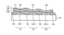
- FIG. 1 illustrates a cross-sectional view of an organic EL device according to an embodiment.
- a device is formed on a substrate 101 having pixel areas 121 , 122 , and 123 .
- a device emitting red is formed at the pixel area 121
- a device emitting green is formed at the pixel area 122
- a device emitting blue is formed at the pixel area 123 .
- the pixel area 121 is referred to as a red emitting device
- the pixel area 122 is referred to as a green emitting device
- the pixel area 123 is referred to as a blue emitting device.
- An arrangement order of pixel areas 121 to 123 is arbitrary. As illustrated in FIG. 1 , the pixel area 121 generating red may be adjacent to the pixel area 122 generating green, allowing an organic layer excluding a light emitting layer to be formed the same at the pixel area 121 generating red and the pixel area 122 generating green. In the organic EL device according to an embodiment, the pixel area 123 generating blue be omitted. That is, only the pixel area 121 generating red and the pixel area 122 generating green may exist.
- a substrate having an insulation characteristic e.g., plastic, quartz, etc.
- the substrate 101 may be formed by a transparent material.
- First electrodes 102 - 1 , 102 - 2 , and 102 - 3 are formed on the substrate 101 to correspond to respective light emitting areas.
- the first electrodes 102 - 1 , 102 - 2 , and 102 - 3 may be formed of a transparent conductive material.
- the first electrodes 102 - 1 , 102 - 2 , and 102 - 3 may be formed of ITO, IZO, and so forth.
- a pixel defining layer 103 for pixel isolation may be formed on the substrate 101 .
- the first electrodes 102 - 1 , 102 - 2 , and 102 - 3 are separated by the pixel defining layer 103 , and a range of the pixel areas 121 , 122 , and 123 are defined by the pixel defining layer 103 .
- An organic insulation layer is used as the pixel defined layer 103 .
- the organic insulation layer may be formed of, e.g., an acrylic resin.
- An organic layer may be formed on the first electrodes 102 - 1 , 102 - 2 , and 102 - 3 and the pixel defined layer 103 .
- a first hole transfer layer 104 may be formed on the first electrodes 102 - 1 , 102 - 2 , and 102 - 3 .
- the first hole transfer layer 104 injects holes in portions, corresponding to the pixel areas 121 , 122 , and 123 , of the organic layer formed on the first hole transfer layer 104 according to voltages applied to the first electrodes 102 - 1 , 102 - 2 , and 102 - 3 .
- the first hole transfer layer 104 may be formed of NPB (Naphthyl.Phenyl.Benzene). In exemplary embodiments, as illustrated in FIG. 1 , the first hole transfer layer 104 may be formed in common at the pixel areas 121 , 122 , and 123 .
- NPB Nephthyl.Phenyl.Benzene
- a second hole transfer layer 105 may be formed on a portion, corresponding to the pixel areas 121 and 122 , of the first hole transfer layer 104 .
- a blue light emitting layer 108 is formed on a portion, corresponding to the pixel area 123 , of the first hole transfer layer 104 .
- a material of the second hole transfer layer 105 may be the same as or different from that of the first hole transfer layer 104 .
- a material of a hole transfer layer may be thickly stacked on the portion corresponding to the pixel areas 121 and 122 according to a thickness of the second hole transfer layer 108 , as compared with the portion corresponding to the pixel area 123 .
- a layer thickness may be suitable for a light extraction condition for an organic EL device according to an embodiment to have a light resonator structure.
- a red light emitting layer 106 is formed on a portion, corresponding to the pixel area 121 , of the hole transfer layer 105
- a green light emitting layer 107 is formed on a portion, corresponding to the pixel area 122 , of the hole transfer layer 105 .
- An electron transfer layer 109 is formed on the red light emitting layer 106 , the green light emitting layer 107 and the blue light emitting layer 108 .
- the electron transfer layer 109 supplies the red light emitting layer 106 , the green light emitting layer 107 and the blue light emitting layer 108 with electrons supplied from a second electrode to be described later.
- the electron transfer layer 109 may be formed of a material such as BCP (bathocuproine).
- BCP bathocuproine
- the electron transfer layer 109 may be formed in common at the pixel areas 121 , 122 , and 123 .
- each of the red light emitting area and the green light emitting area in common, has such a structure that a first electrode having a light transmitting characteristic, an organic layer formed on the first electrode, and a second electrode having a light reflecting characteristic are stacked.
- hole and electron transfer layers of the organic layer are formed using the same material, and a process of forming the organic layer is simplified.
- a second electrode 111 may be disposed on the electron transfer layer 109 to be formed in common at the pixel areas 121 , 122 , and 123 .
- the second electrode 111 may be formed of a material having a light reflecting characteristic.
- the second electrode 111 may be formed of a metallic material.
- the second electrode 111 may be formed of aluminum (Al).
- a layer 110 is formed on a port, corresponding to the pixel area 121 , of the electron transfer layer 109 using a material having a reflecting characteristic and different from a material of the second electrode 111 .
- the layer 110 may be formed of a material of improving reflectance of red light in combination with a material having a reflecting characteristic of the second electrode 111 .
- red reflectance from the layer 110 and the second electrode 111 combined may be larger than that from the second electrode 111 alone.
- reflectance of light having a wavelength of 550 nm from the layer 110 and the second electrode 111 combined may be smaller than that from the second electrode 111 alone.
- FIG. 2 illustrates a result of measurement on reflectance of light having a wavelength of 620 nm when an aluminum layer and a copper layer are combined and in a case where only an aluminum layer is used.
- the horizontal axis is reflectance and the vertical axis is the thickness of the copper layer in nanometers.
- a reference numeral 201 shows a result of measurement on reflectance of light when a copper layer is formed on one surface of an aluminum layer and light having a wavelength of 620 nm is provided to the copper layer side.
- a thickness of the aluminum layer is about 120 nm and reflects most visible light.
- a thickness of the copper layer is varied from 5 nm to 50 nm.
- a reference numeral 202 shows a result of measurement on reflectance of light having a wavelength of 620 nm in the event that an aluminum layer is only used.
- a thickness of the aluminum layer is about 120 nm that reflects most visible light. Since no copper layer exists, reflectance does not follow a thickness of the copper layer of a horizontal axis. That is, the reflectance has a constant value.
- reflectance of copper is larger than that of aluminum in a domain of light the wavelength of which is more than 630 nm, and reflectance is reduced in a green and red light domain. Since an emission peak wavelength of a red light emitting layer is around 620 nm, it is difficult to improve reflectance of red only using a copper layer.
- a thickness of a copper layer is between 5 nm and 50 nm, reflectance of light having a wavelength of 620 nm in a case where an aluminum layer and a copper layer are combined is improved as compared with the case when the aluminum layer is only used.
- reflectance is improved by 12% as compared with the case when the aluminum layer is only used.
- FIG. 3 illustrates a result of measurement on reflectance of light having a wavelength of 550 nm in a case where an aluminum layer and a copper layer are combined and in a case where an aluminum layer is only used.
- the horizontal axis is reflectance and the vertical axis is the thickness of the copper layer in nanometers.
- a reference numeral 302 shows a result of measurement on reflectance of light in the event that a copper layer is formed on one surface of an aluminum layer and a light having a wavelength of 550 nm is incident on a copper layer side.
- a reference numeral 301 shows a result of measurement on reflectance of light having a wavelength of 550 nm in the event that an aluminum layer is only used.
- Each of the aluminum layer and the copper layer has the same thickness as described with reference to FIG. 2 .
- the second electrode 111 includes a material such as aluminum (Al)
- a copper layer 110 is formed on an electron transfer layer 109 that is formed on a red light emitting layer 106 .
- the copper layer 110 is not formed on the electron transfer layer 109 that is formed on a green light emitting layer 107 and a blue light emitting layer 108 .
- the second electrode 111 may be formed to have a thickness of 120 nm that reflects most visible light and a thickness of the copper layer 110 may be between 5 nm and 50 nm. If the thickness of the copper layer 110 is less than 5 nm, reflectance of the copper layer 110 is insufficient and an effect obtained by using the copper layer 110 is reduced. In practice, in the event that the thickness of the copper layer 110 is less than 5 nm, brightness is reduced although an x value of CIE1931(x, y) chromaticity is decreased, in comparison with the case that the thickness of the copper layer 110 is 10 nm.
- the thickness of the copper layer 110 exceeds 50 nm, reflectance of light having a wavelength of 620 nm is reduced in comparison with that of aluminum alone. Also, having a thinner copper layer 110 reduces time taken to form the copper layer 110 on the electron transfer layer 109 formed on a red light emitting layer 106 , the amount of material used, and maintenance of a layer forming apparatus.
- silver (Ag) may be used as a material of the second electrode 111 and copper (Cu) may be used as a material of the layer 110 .
- copper (Cu) may be used as a material of the layer 110 .
- aluminum (Al) may be used as a material of the second electrode 111 and gold (Au) may be used as a material of the layer 110 .
- gold (Au) may be used as a material of the layer 110 .
- alloy of different metals may be used as the second electrode 111 and the layer 110 to prevent generation of migration or defect.
- a bottom emission type of organic EL device according to an embodiment has been described above. However, embodiments are applicable to a top emission type of organic EL device.
- the following table 1 shows light emitting brightness, CIE1931(x, y) chromaticity, a driving voltage having a current density of 10 mA/cm 2 , and a driving voltage having a current density of 100 mA/cm 2 when a quartz substrate is used as a substrate 101 , an ITO layer having a thickness of 70 nm is used as first electrodes 102 - 1 , 102 - 2 , and 102 - 3 , an NPB layer having a thickness of 155 nm is used as a first hole transfer layer 104 , an NPB layer having a thickness of 85 nm is used as a second hole transfer layer 105 , a red light emitting layer 106 has a layer thickness of 40 nm, a green light emitting layer 107 has a thickness of 20 nm, a blue light emitting layer 108 has a layer thickness of 20 nm, a BCP layer having a thickness of 30 nm, an LiF layer having a thickness
- a thickness of a copper layer used as a layer 110 is sequentially changed from 0 nm (i.e., the case that the layer 110 does not exist) to 5 nm, 10 nm, 20 nm, 30 nm, 50 nm, and 100 nm.
- a blank of the driving voltage means that the driving voltage is not measured.
- the following table 2 shows light emitting brightness, CIE1931(x, y) chromaticity, a driving voltage having a current density of 10 mA/cm 2 and a driving voltage having a current density of 100 mA/cm 2 with respect to an organic EL device according to a comparative example shown in FIG. 4 .
- FIG. 4 illustrates different from FIG. 1 in that a hole transfer layer 105 - 2 is further formed under a red light emitting layer 106 . Also, in FIG. 4 , the hole transfer layer 105 - 2 has a thickness of 40 nm. Also, in FIG. 4 , a layer 110 is not used.
- Driving voltage Light emitting having a current having a current brightness density of density of (cd m ⁇ 2) chromaticity 10 mA/cm 2 100 mA/cm 2 1.2637e+003 (6.7128e ⁇ 001, 5.8 10.3 3.2849e ⁇ 001)
- a thickness of a copper layer is between 5 nm and 50 nm, in particular, when a thickness of a copper layer is between 20 nm and 30 nm, brightness of an organic EL device according to an embodiment is higher than that of an organic EL device according to the comparative example. Also, in an organic EL device according to an embodiment, a driving voltage for the same current density is reduced by 0.8V. The reason is that a thickness of an organic layer is thinner than that of an organic EL device according to the comparative example.
- Improvement of resolution and display brightness of a display device using an organic EL device is required, and a current density of 100 mA/cm 2 need be considered as a peak value. Under this situation, a driving voltage is lowered from 10.3V to 8.5V, that is, by 1.8V. Thus, it is possible to implement a low-power and long-life display device.
- an organic EL device includes a second electrode that efficiently reflects light generated by an organic layer of the red light emitting area, improving light extraction efficiency. Also, a thickness of the organic layer of the red light emitting area may be reduced as compared with that according to the conventional art, allowing a decrease in a driving voltage and fabrication cost.
- red light extraction efficiency may be further improved as compared with the case that a layer formed of a material including aluminum or silver is only used.
- the organic layers of the red and green light emitting areas may be used in common except for a light emitting layer.
- a process of forming an organic layer is simplified, and an increase in a fabrication cost of an organic EL device is suppressed.
Landscapes
- Physics & Mathematics (AREA)
- Optics & Photonics (AREA)
- Electroluminescent Light Sources (AREA)
Abstract
Description
- Japanese Patent Application No. 2012-263666, filed on Nov. 30, 2012, in the Japanese Intellectual Property Office, and entitled: “ORGANIC ELECTROLUMINESCENCE DEVICE,” is incorporated by reference herein in its entirety.
- 1. Field
- Embodiments relate to an organic electroluminescence (hereinafter, referred to as EL) device.
- 2. Description of the Related Art
- An organic EL device receives attention as a light emitting device. The organic EL device is a self-emissive device in which an organic layer including a light emitting layer, disposed between an anode electrode and a cathode electrode, emits light when holes and electrons, generated when voltages are supplied to the anode and cathode electrodes, are combined.
- In the organic EL element, a technique is proposed which makes a characteristic of each of R, G and B pixels become uniform when an image is displayed using pixels emitting red (R), green (G) and blue (B), e.g., in which a thickness of an organic layer of a red pixel increases, thus increasing the fabrication cost and the driving voltage.
- One or more embodiments is directed to provide an organic EL device which includes a red light emitting area including a first electrode having a light transmitting characteristic and an organic layer, the first electrode and the organic layer being stacked; a green light emitting area including a first electrode having a light transmitting characteristic and an organic layer, the first electrode and the organic layer being stacked; and a second electrode disposed on the organic layer of the red light emitting area and on the organic layer of the green light emitting area and having a light reflecting characteristic. Reflectance of green light, e.g., having a wavelength of 550 nm, by the second electrode of the red light emitting area is smaller than reflectance of green light by the second electrode of the green light emitting area. Reflectance of red light, e.g., having a wavelength of 620 nm, by the second electrode of the red light emitting area is larger than reflectance of red light by the second electrode of the green light emitting area.
- The second electrode of the red light emitting area may include a layer including copper and formed on the organic layer of the red light emitting area.
- A thickness of the layer including the copper may be between 5 nm and 50 nm and the second electrode of the red light emitting area may be formed on the layer including the copper and of a material including aluminum or silver.
- The second electrode of the red light emitting area may have a layer including gold. The second electrode of the red light emitting area may be formed on the layer including gold and of a material including aluminum or silver.
- The organic layers of the red and green light emitting areas may be used in common except for a light emitting layer.
- Features will become apparent to those of skill in the art by describing in detail exemplary embodiments with reference to the attached drawings in which:
-
FIG. 1 illustrates a cross-sectional view of an organic EL device according to an embodiment; -
FIG. 2 illustrates a graph showing a relation between a thickness of a copper layer and reflectance of light having a wavelength of 620 nm; -
FIG. 3 illustrates a graph showing a relation between a thickness of a copper layer and reflectance of light having a wavelength of 550 nm; and -
FIG. 4 illustrates a cross-sectional view of an organic EL device according to a comparative example. - Example embodiments will now be described more fully hereinafter with reference to the accompanying drawings; however, they may be embodied in different forms and should not be construed as limited to the embodiments set forth herein. Rather, these embodiments are provided so that this disclosure will be thorough and complete, and will fully convey exemplary implementations to those skilled in the art.
- It will be understood that, although the terms “first”, “second”, “third”, etc., may be used herein to describe various elements, components, regions, layers and/or sections, these elements, components, regions, layers and/or sections should not be limited by these terms. These terms are only used to distinguish one element, component, region, layer or section from another region, layer or section. Thus, a first element, component, region, layer or section discussed below could be termed a second element, component, region, layer or section without departing from the teachings herein.
- Spatially relative terms, such as “beneath”, “below”, “lower”, “under”, “above”, “upper” and the like, may be used herein for ease of description to describe one element or feature's relationship to another element(s) or feature(s) as illustrated in the figures. It will be understood that the spatially relative terms are intended to encompass different orientations of the device in use or operation in addition to the orientation depicted in the figures. For example, if the device in the figures is turned over, elements described as “below” or “beneath” or “under” other elements or features would then be oriented “above” the other elements or features. Thus, the exemplary terms “below” and “under” can encompass both an orientation of above and below. The device may be otherwise oriented (rotated 90 degrees or at other orientations) and the spatially relative descriptors used herein interpreted accordingly. In addition, it will also be understood that when a layer is referred to as being “between” two layers, it can be the only layer between the two layers, or one or more intervening layers may also be present.
- The terminology used herein is for the purpose of describing particular embodiments only and is not intended to be limiting. As used herein, the singular forms “a”, “an” and “the” are intended to include the plural forms as well, unless the context clearly indicates otherwise. It will be further understood that the terms “comprises” and/or “comprising,” when used in this specification, specify the presence of stated features, integers, steps, operations, elements, and/or components, but do not preclude the presence or addition of one or more other features, integers, steps, operations, elements, components, and/or groups thereof. As used herein, the term “and/or” includes any and all combinations of one or more of the associated listed items. Also, the term “exemplary” is intended to refer to an example or illustration.
- It will be understood that when an element or layer is referred to as being “on”, “connected to”, “coupled to”, or “adjacent to” another element or layer, it can be directly on, connected, coupled, or adjacent to the other element or layer, or intervening elements or layers may be present. In contrast, when an element is referred to as being “directly on,” “directly connected to”, “directly coupled to”, or “immediately adjacent to” another element or layer, there are no intervening elements or layers present.
- Unless otherwise defined, all terms (including technical and scientific terms) used herein have the same meaning as commonly understood by one of ordinary skill in the art to which this disclosure belongs. It will be further understood that terms, such as those defined in commonly used dictionaries, should be interpreted as having a meaning that is consistent with their meaning in the context of the relevant art and/or the present specification and will not be interpreted in an idealized or overly formal sense unless expressly so defined herein.
-
FIG. 1 illustrates a cross-sectional view of an organic EL device according to an embodiment. InFIG. 1 , a device is formed on asubstrate 101 havingpixel areas pixel area 121, a device emitting green is formed at thepixel area 122, and a device emitting blue is formed at thepixel area 123. Thepixel area 121 is referred to as a red emitting device, thepixel area 122 is referred to as a green emitting device, and thepixel area 123 is referred to as a blue emitting device. - An arrangement order of
pixel areas 121 to 123 is arbitrary. As illustrated inFIG. 1 , thepixel area 121 generating red may be adjacent to thepixel area 122 generating green, allowing an organic layer excluding a light emitting layer to be formed the same at thepixel area 121 generating red and thepixel area 122 generating green. In the organic EL device according to an embodiment, thepixel area 123 generating blue be omitted. That is, only thepixel area 121 generating red and thepixel area 122 generating green may exist. - A substrate having an insulation characteristic, e.g., plastic, quartz, etc., may be used as the
substrate 101. Since a bottom emission type of organic EL device is mainly described as an embodiment, thesubstrate 101 may be formed by a transparent material. - First electrodes 102-1, 102-2, and 102-3 are formed on the
substrate 101 to correspond to respective light emitting areas. In case of a bottom emission type of organic EL device according to an embodiment, the first electrodes 102-1, 102-2, and 102-3 may be formed of a transparent conductive material. For example, the first electrodes 102-1, 102-2, and 102-3 may be formed of ITO, IZO, and so forth. - A
pixel defining layer 103 for pixel isolation may be formed on thesubstrate 101. The first electrodes 102-1, 102-2, and 102-3 are separated by thepixel defining layer 103, and a range of thepixel areas pixel defining layer 103. An organic insulation layer is used as the pixel definedlayer 103. The organic insulation layer may be formed of, e.g., an acrylic resin. - An organic layer may be formed on the first electrodes 102-1, 102-2, and 102-3 and the pixel defined
layer 103. In detail, a firsthole transfer layer 104 may be formed on the first electrodes 102-1, 102-2, and 102-3. The firsthole transfer layer 104 injects holes in portions, corresponding to thepixel areas hole transfer layer 104 according to voltages applied to the first electrodes 102-1, 102-2, and 102-3. For example, the firsthole transfer layer 104 may be formed of NPB (Naphthyl.Phenyl.Benzene). In exemplary embodiments, as illustrated inFIG. 1 , the firsthole transfer layer 104 may be formed in common at thepixel areas - In exemplary embodiments, a second
hole transfer layer 105 may be formed on a portion, corresponding to thepixel areas hole transfer layer 104. Also, a bluelight emitting layer 108 is formed on a portion, corresponding to thepixel area 123, of the firsthole transfer layer 104. A material of the secondhole transfer layer 105 may be the same as or different from that of the firsthole transfer layer 104. Thus, a material of a hole transfer layer may be thickly stacked on the portion corresponding to thepixel areas hole transfer layer 108, as compared with the portion corresponding to thepixel area 123. A layer thickness may be suitable for a light extraction condition for an organic EL device according to an embodiment to have a light resonator structure. - A red
light emitting layer 106 is formed on a portion, corresponding to thepixel area 121, of thehole transfer layer 105, and a greenlight emitting layer 107 is formed on a portion, corresponding to thepixel area 122, of thehole transfer layer 105. - An
electron transfer layer 109 is formed on the redlight emitting layer 106, the greenlight emitting layer 107 and the bluelight emitting layer 108. Theelectron transfer layer 109 supplies the redlight emitting layer 106, the greenlight emitting layer 107 and the bluelight emitting layer 108 with electrons supplied from a second electrode to be described later. For example, theelectron transfer layer 109 may be formed of a material such as BCP (bathocuproine). In exemplary embodiments, as illustrated inFIG. 1 , theelectron transfer layer 109 may be formed in common at thepixel areas - As described above, each of the red light emitting area and the green light emitting area according to an embodiment, in common, has such a structure that a first electrode having a light transmitting characteristic, an organic layer formed on the first electrode, and a second electrode having a light reflecting characteristic are stacked. In particular, hole and electron transfer layers of the organic layer are formed using the same material, and a process of forming the organic layer is simplified.
- A
second electrode 111 may be disposed on theelectron transfer layer 109 to be formed in common at thepixel areas second electrode 111 may be formed of a material having a light reflecting characteristic. For example, thesecond electrode 111 may be formed of a metallic material. In detail, thesecond electrode 111 may be formed of aluminum (Al). - In exemplary embodiments, a
layer 110 is formed on a port, corresponding to thepixel area 121, of theelectron transfer layer 109 using a material having a reflecting characteristic and different from a material of thesecond electrode 111. Thelayer 110 may be formed of a material of improving reflectance of red light in combination with a material having a reflecting characteristic of thesecond electrode 111. - In particular, to improve reflectance of red light, e.g., light having a wavelength of 620 nm, red reflectance from the
layer 110 and thesecond electrode 111 combined may be larger than that from thesecond electrode 111 alone. Further, reflectance of light having a wavelength of 550 nm from thelayer 110 and thesecond electrode 111 combined may be smaller than that from thesecond electrode 111 alone. -
FIG. 2 illustrates a result of measurement on reflectance of light having a wavelength of 620 nm when an aluminum layer and a copper layer are combined and in a case where only an aluminum layer is used. InFIG. 2 , the horizontal axis is reflectance and the vertical axis is the thickness of the copper layer in nanometers. - A
reference numeral 201 shows a result of measurement on reflectance of light when a copper layer is formed on one surface of an aluminum layer and light having a wavelength of 620 nm is provided to the copper layer side. In this case, a thickness of the aluminum layer is about 120 nm and reflects most visible light. A thickness of the copper layer is varied from 5 nm to 50 nm. - A
reference numeral 202 shows a result of measurement on reflectance of light having a wavelength of 620 nm in the event that an aluminum layer is only used. In this case, a thickness of the aluminum layer is about 120 nm that reflects most visible light. Since no copper layer exists, reflectance does not follow a thickness of the copper layer of a horizontal axis. That is, the reflectance has a constant value. - In general, reflectance of copper is larger than that of aluminum in a domain of light the wavelength of which is more than 630 nm, and reflectance is reduced in a green and red light domain. Since an emission peak wavelength of a red light emitting layer is around 620 nm, it is difficult to improve reflectance of red only using a copper layer.
- As illustrated in
FIG. 2 , however, if a thickness of a copper layer is between 5 nm and 50 nm, reflectance of light having a wavelength of 620 nm in a case where an aluminum layer and a copper layer are combined is improved as compared with the case when the aluminum layer is only used. In particular, in the event that a thickness of the copper layer is 30 nm, reflectance is improved by 12% as compared with the case when the aluminum layer is only used. -
FIG. 3 illustrates a result of measurement on reflectance of light having a wavelength of 550 nm in a case where an aluminum layer and a copper layer are combined and in a case where an aluminum layer is only used. InFIG. 3 , the horizontal axis is reflectance and the vertical axis is the thickness of the copper layer in nanometers. - A
reference numeral 302 shows a result of measurement on reflectance of light in the event that a copper layer is formed on one surface of an aluminum layer and a light having a wavelength of 550 nm is incident on a copper layer side. Areference numeral 301 shows a result of measurement on reflectance of light having a wavelength of 550 nm in the event that an aluminum layer is only used. Each of the aluminum layer and the copper layer has the same thickness as described with reference toFIG. 2 . - It is understood from
FIG. 3 that reflectance of light having a wavelength of 550 nm is reduced in proportion to an increase in thickness of copper. - Here, in the event that the
second electrode 111 according to an embodiment of includes a material such as aluminum (Al), acopper layer 110 is formed on anelectron transfer layer 109 that is formed on a redlight emitting layer 106. Also, thecopper layer 110 is not formed on theelectron transfer layer 109 that is formed on a greenlight emitting layer 107 and a bluelight emitting layer 108. - The
second electrode 111 may be formed to have a thickness of 120 nm that reflects most visible light and a thickness of thecopper layer 110 may be between 5 nm and 50 nm. If the thickness of thecopper layer 110 is less than 5 nm, reflectance of thecopper layer 110 is insufficient and an effect obtained by using thecopper layer 110 is reduced. In practice, in the event that the thickness of thecopper layer 110 is less than 5 nm, brightness is reduced although an x value of CIE1931(x, y) chromaticity is decreased, in comparison with the case that the thickness of thecopper layer 110 is 10 nm. - If the thickness of the
copper layer 110 exceeds 50 nm, reflectance of light having a wavelength of 620 nm is reduced in comparison with that of aluminum alone. Also, having athinner copper layer 110 reduces time taken to form thecopper layer 110 on theelectron transfer layer 109 formed on a redlight emitting layer 106, the amount of material used, and maintenance of a layer forming apparatus. - Alternatively, silver (Ag) may be used as a material of the
second electrode 111 and copper (Cu) may be used as a material of thelayer 110. As another alternative, aluminum (Al) may be used as a material of thesecond electrode 111 and gold (Au) may be used as a material of thelayer 110. As yet another alternative, silver (Ag) may be used as a material of thesecond electrode 111 and gold (Au) may be used as a material of thelayer 110. Also, alloy of different metals may be used as thesecond electrode 111 and thelayer 110 to prevent generation of migration or defect. - A bottom emission type of organic EL device according to an embodiment has been described above. However, embodiments are applicable to a top emission type of organic EL device.
- (Measurement)
- Below, a result of measuring light emitting efficiency of an organic EL device according to an embodiment and a result of measuring light emitting efficiency of an organic EL device according to the prior art are described.
- The following table 1 shows light emitting brightness, CIE1931(x, y) chromaticity, a driving voltage having a current density of 10 mA/cm2, and a driving voltage having a current density of 100 mA/cm2 when a quartz substrate is used as a
substrate 101, an ITO layer having a thickness of 70 nm is used as first electrodes 102-1, 102-2, and 102-3, an NPB layer having a thickness of 155 nm is used as a firsthole transfer layer 104, an NPB layer having a thickness of 85 nm is used as a secondhole transfer layer 105, a redlight emitting layer 106 has a layer thickness of 40 nm, a greenlight emitting layer 107 has a thickness of 20 nm, a bluelight emitting layer 108 has a layer thickness of 20 nm, a BCP layer having a thickness of 30 nm, an LiF layer having a thickness of 1 nm are used as anelectron transfer layer 109, and an aluminum layer having a thickness of 120 nm is used as asecond electrode 111. A thickness of a copper layer used as alayer 110 is sequentially changed from 0 nm (i.e., the case that thelayer 110 does not exist) to 5 nm, 10 nm, 20 nm, 30 nm, 50 nm, and 100 nm. In the table 1, a blank of the driving voltage means that the driving voltage is not measured. -
TABLE 1 Driving voltage Thickness Driving voltage (V) having of Cu Emission (V) having a a current layer brightness CIE1931(x, y) current density density of (nm) (cd m−2) chromaticity of 10 mA/cm2 100 mA/ cm 20 1.2200e+003 (6.5971e−001, 4.9 3.4000e−001) 5 1.2771e+003 (6.6050e−001, 5.1 3.3921e−001) 10 1.3128e+003 (6.6140e−001, 5.0 3.3832e−001) 20 1.3387e+003 (6.6311e−001, 5.0 3.3662e−001) 30 1.3352e+003 (6.6440e−001, 5.0 8.5 3.3533e−001) 50 1.3147e+003 (6.6580e−001, 5.0 3.3394e−001) 100 1.2970e+003 (6.6651e−001, 5.0 3.3323e−001) - Like table 1, the following table 2 shows light emitting brightness, CIE1931(x, y) chromaticity, a driving voltage having a current density of 10 mA/cm2 and a driving voltage having a current density of 100 mA/cm2 with respect to an organic EL device according to a comparative example shown in
FIG. 4 . -
FIG. 4 illustrates different fromFIG. 1 in that a hole transfer layer 105-2 is further formed under a redlight emitting layer 106. Also, inFIG. 4 , the hole transfer layer 105-2 has a thickness of 40 nm. Also, inFIG. 4 , alayer 110 is not used. -
TABLE 2 Driving voltage (V) Driving voltage (V) Light emitting having a current having a current brightness density of density of (cd m−2) chromaticity 10 mA/cm2 100 mA/cm2 1.2637e+003 (6.7128e−001, 5.8 10.3 3.2849e−001) - Referring to the tables 1 and 2, when a thickness of a copper layer is between 5 nm and 50 nm, in particular, when a thickness of a copper layer is between 20 nm and 30 nm, brightness of an organic EL device according to an embodiment is higher than that of an organic EL device according to the comparative example. Also, in an organic EL device according to an embodiment, a driving voltage for the same current density is reduced by 0.8V. The reason is that a thickness of an organic layer is thinner than that of an organic EL device according to the comparative example.
- Improvement of resolution and display brightness of a display device using an organic EL device is required, and a current density of 100 mA/cm2 need be considered as a peak value. Under this situation, a driving voltage is lowered from 10.3V to 8.5V, that is, by 1.8V. Thus, it is possible to implement a low-power and long-life display device.
- By way of summation and review, according to embodiments, an organic EL device includes a second electrode that efficiently reflects light generated by an organic layer of the red light emitting area, improving light extraction efficiency. Also, a thickness of the organic layer of the red light emitting area may be reduced as compared with that according to the conventional art, allowing a decrease in a driving voltage and fabrication cost.
- Additionally, for example, when the red light emitting area includes a layer formed of a material including copper having a thickness between 5 nm and 50 nm, red light extraction efficiency may be further improved as compared with the case that a layer formed of a material including aluminum or silver is only used.
- Further, the organic layers of the red and green light emitting areas may be used in common except for a light emitting layer. In this case, a process of forming an organic layer is simplified, and an increase in a fabrication cost of an organic EL device is suppressed.
- Example embodiments have been disclosed herein, and although specific terms are employed, they are used and are to be interpreted in a generic and descriptive sense only and not for purpose of limitation. In some instances, as would be apparent to one of ordinary skill in the art as of the filing of the present application, features, characteristics, and/or elements described in connection with a particular embodiment may be used singly or in combination with features, characteristics, and/or elements described in connection with other embodiments unless otherwise specifically indicated. Accordingly, it will be understood by those of skill in the art that various changes in form and details may be made without departing from the spirit and scope of the present invention as set forth in the following claims.
Claims (9)
Applications Claiming Priority (2)
| Application Number | Priority Date | Filing Date | Title |
|---|---|---|---|
| JP2012-263666 | 2012-11-30 | ||
| JP2012263666A JP2014110143A (en) | 2012-11-30 | 2012-11-30 | Organic el element |
Publications (2)
| Publication Number | Publication Date |
|---|---|
| US20140151663A1 true US20140151663A1 (en) | 2014-06-05 |
| US9147714B2 US9147714B2 (en) | 2015-09-29 |
Family
ID=50824570
Family Applications (1)
| Application Number | Title | Priority Date | Filing Date |
|---|---|---|---|
| US14/092,327 Active US9147714B2 (en) | 2012-11-30 | 2013-11-27 | Organic electroluminescence device |
Country Status (3)
| Country | Link |
|---|---|
| US (1) | US9147714B2 (en) |
| JP (1) | JP2014110143A (en) |
| KR (1) | KR102115567B1 (en) |
Cited By (1)
| Publication number | Priority date | Publication date | Assignee | Title |
|---|---|---|---|---|
| WO2016041860A1 (en) * | 2014-09-18 | 2016-03-24 | Osram Oled Gmbh | Organic light-emitting diode and lighting device |
Families Citing this family (1)
| Publication number | Priority date | Publication date | Assignee | Title |
|---|---|---|---|---|
| KR102397823B1 (en) * | 2015-11-30 | 2022-05-12 | 엘지디스플레이 주식회사 | Organic light emitting display device |
Citations (27)
| Publication number | Priority date | Publication date | Assignee | Title |
|---|---|---|---|---|
| US20040217694A1 (en) * | 2003-04-30 | 2004-11-04 | Eastman Kodak Company | Color oled display with improved power efficiency |
| US20050280355A1 (en) * | 2004-06-18 | 2005-12-22 | Kwan-Hee Lee | Organic light emitting display device and method of fabricating the same |
| US20060105201A1 (en) * | 2004-11-12 | 2006-05-18 | Jun-Yeob Lee | Organic electroluminescent device |
| US20070075310A1 (en) * | 2005-09-30 | 2007-04-05 | Jun-Yeob Lee | Organic light-emitting display device and method of manufacturing the same |
| US20070296334A1 (en) * | 2006-06-23 | 2007-12-27 | Canon Kabushiki Kaisha | Organic light-emitting device |
| US20080292994A1 (en) * | 2007-05-21 | 2008-11-27 | Sony Corporation | Transfer method, transfer apparatus, and method of manufacturing organic light emitting element |
| US20090325451A1 (en) * | 2008-06-25 | 2009-12-31 | Sony Corporation | Donor substrate and method of manufacturing display |
| US20110085325A1 (en) * | 2008-06-26 | 2011-04-14 | Daniel David Lecloux | Organic light-emitting diode luminaires |
| US20110204335A1 (en) * | 2009-08-24 | 2011-08-25 | E. I. Du Pont De Nemours And Company | Organic light-emitting diode luminaires |
| US20110204338A1 (en) * | 2009-08-24 | 2011-08-25 | E. I. Du Pont De Nemours And Company | Organic light-emitting diode luminaires |
| US20110204336A1 (en) * | 2009-08-24 | 2011-08-25 | E.I. Du Pont De Nemours And Company | Organic light-emitting diode luminaires |
| US20110204340A1 (en) * | 2009-08-24 | 2011-08-25 | E.I. Du Pont De Nemours And Company | Organic light-emitting diode luminaires |
| US20110241000A1 (en) * | 2010-03-30 | 2011-10-06 | Jong-Hyun Choi | Organic light-emitting display apparatus and method of manufacturing the same |
| US20120073735A1 (en) * | 2006-04-06 | 2012-03-29 | Sony Corporation | Red organic light emitting element and display device provided with same, donor substrate and transfer method using same, method of manufacturing display device, and system of manufacturing display device |
| US20120235178A1 (en) * | 2011-03-16 | 2012-09-20 | Sony Corporation | Display device and electronic apparatus |
| US20120298968A1 (en) * | 2011-05-23 | 2012-11-29 | Samsung Mobile Display Co., Ltd. | Organic light-emitting device |
| US20130075768A1 (en) * | 2011-09-22 | 2013-03-28 | Lg Display Co., Ltd. | Organic Light Emitting Diode Display Device and Method of Fabricating the Same |
| US20130105778A1 (en) * | 2011-11-01 | 2013-05-02 | Lg Display Co., Ltd. | Organic light-emitting diode display device |
| US20130161590A1 (en) * | 2011-12-26 | 2013-06-27 | Samsung Display Co., Ltd. | Organic light emitting device with enhanced lifespan |
| US20130168653A1 (en) * | 2011-12-30 | 2013-07-04 | Lg Display Co., Ltd. | Organic light emitting device and method for manufacturing the same |
| US20130168652A1 (en) * | 2011-12-30 | 2013-07-04 | Lg Display Co., Ltd. | Organic Light Emitting Device and Method for Manufacturing the Same |
| US20130187132A1 (en) * | 2012-01-19 | 2013-07-25 | Sony Corporation | Display and method of manufacturing the same, unit, transfer printing method, organic electroluminescence unit and method of manufacturing the same, and electronic apparatus |
| US20130200780A1 (en) * | 2012-02-06 | 2013-08-08 | Samsung Mobile Display Co., Ltd. | Organic light emitting display devices and methods of manufacturing organic light emitting display devices |
| US20130207084A1 (en) * | 2012-02-13 | 2013-08-15 | Samsung Display Co., Ltd. | Organic light emitting diode display and method for manufacturing the same |
| US20140235004A1 (en) * | 2013-02-18 | 2014-08-21 | Samsung Display Co., Ltd. | Method of manufacturing organic light emitting display |
| US20140231753A1 (en) * | 2013-02-19 | 2014-08-21 | Au Optronics Corporation | Multi-color light emitting diode and method for making same |
| US20140291627A1 (en) * | 2013-03-26 | 2014-10-02 | Samsung Display Co., Ltd. | Organic light-emitting display device, method of manufacturing the same, and donor substrate and donor substrate set used to manufacture the organic light-emitting display device |
Family Cites Families (11)
| Publication number | Priority date | Publication date | Assignee | Title |
|---|---|---|---|---|
| JPH0627853A (en) | 1992-07-10 | 1994-02-04 | Hitachi Koki Co Ltd | Heat fixing machine |
| JP2846571B2 (en) | 1994-02-25 | 1999-01-13 | 出光興産株式会社 | Organic electroluminescence device |
| TW463528B (en) | 1999-04-05 | 2001-11-11 | Idemitsu Kosan Co | Organic electroluminescence element and their preparation |
| KR100875097B1 (en) | 2002-09-18 | 2008-12-19 | 삼성모바일디스플레이주식회사 | Organic electroluminescent device using optical resonance effect |
| US20040149984A1 (en) | 2003-01-31 | 2004-08-05 | Eastman Kodak Company | Color OLED display with improved emission |
| JP4566759B2 (en) | 2005-01-24 | 2010-10-20 | 東北パイオニア株式会社 | Organic EL panel |
| JP4402069B2 (en) | 2006-03-31 | 2010-01-20 | キヤノン株式会社 | Multicolor organic EL display |
| JP2009064703A (en) | 2007-09-07 | 2009-03-26 | Sony Corp | Organic light emitting display |
| JP5217791B2 (en) * | 2007-10-18 | 2013-06-19 | セイコーエプソン株式会社 | LIGHT EMITTING DEVICE AND ELECTRONIC DEVICE |
| JP5212095B2 (en) | 2008-12-26 | 2013-06-19 | 大日本印刷株式会社 | Organic electroluminescence device and method for producing the same |
| KR101174875B1 (en) | 2010-01-14 | 2012-08-17 | 삼성디스플레이 주식회사 | Apparatus for thin layer deposition, method for manufacturing of organic light emitting display apparatus using the same, and organic light emitting display apparatus manufactured by the method |
-
2012
- 2012-11-30 JP JP2012263666A patent/JP2014110143A/en active Pending
-
2013
- 2013-11-06 KR KR1020130134232A patent/KR102115567B1/en active Active
- 2013-11-27 US US14/092,327 patent/US9147714B2/en active Active
Patent Citations (31)
| Publication number | Priority date | Publication date | Assignee | Title |
|---|---|---|---|---|
| US20040217694A1 (en) * | 2003-04-30 | 2004-11-04 | Eastman Kodak Company | Color oled display with improved power efficiency |
| US7470933B2 (en) * | 2004-06-18 | 2008-12-30 | Samsung Sdi Co., Ltd. | Organic light emitting display device |
| US20050280355A1 (en) * | 2004-06-18 | 2005-12-22 | Kwan-Hee Lee | Organic light emitting display device and method of fabricating the same |
| US20060105201A1 (en) * | 2004-11-12 | 2006-05-18 | Jun-Yeob Lee | Organic electroluminescent device |
| US20070075310A1 (en) * | 2005-09-30 | 2007-04-05 | Jun-Yeob Lee | Organic light-emitting display device and method of manufacturing the same |
| US20090263924A1 (en) * | 2005-09-30 | 2009-10-22 | Samsung Mobile Display Co., Ltd. | Organic Light-Emitting Display Device and Method of Manufacturing the Same |
| US20120073735A1 (en) * | 2006-04-06 | 2012-03-29 | Sony Corporation | Red organic light emitting element and display device provided with same, donor substrate and transfer method using same, method of manufacturing display device, and system of manufacturing display device |
| US20070296334A1 (en) * | 2006-06-23 | 2007-12-27 | Canon Kabushiki Kaisha | Organic light-emitting device |
| US20080292994A1 (en) * | 2007-05-21 | 2008-11-27 | Sony Corporation | Transfer method, transfer apparatus, and method of manufacturing organic light emitting element |
| US20090325451A1 (en) * | 2008-06-25 | 2009-12-31 | Sony Corporation | Donor substrate and method of manufacturing display |
| US20130202812A1 (en) * | 2008-06-25 | 2013-08-08 | Sony Corporation | Donor substrate and method of manufacturing display |
| US20110206868A1 (en) * | 2008-06-25 | 2011-08-25 | Sony Corporation | Donor substrate and method of manufacturing display |
| US20110085325A1 (en) * | 2008-06-26 | 2011-04-14 | Daniel David Lecloux | Organic light-emitting diode luminaires |
| US20110204340A1 (en) * | 2009-08-24 | 2011-08-25 | E.I. Du Pont De Nemours And Company | Organic light-emitting diode luminaires |
| US20110204335A1 (en) * | 2009-08-24 | 2011-08-25 | E. I. Du Pont De Nemours And Company | Organic light-emitting diode luminaires |
| US20110204338A1 (en) * | 2009-08-24 | 2011-08-25 | E. I. Du Pont De Nemours And Company | Organic light-emitting diode luminaires |
| US20110204336A1 (en) * | 2009-08-24 | 2011-08-25 | E.I. Du Pont De Nemours And Company | Organic light-emitting diode luminaires |
| US20110241000A1 (en) * | 2010-03-30 | 2011-10-06 | Jong-Hyun Choi | Organic light-emitting display apparatus and method of manufacturing the same |
| US20120235178A1 (en) * | 2011-03-16 | 2012-09-20 | Sony Corporation | Display device and electronic apparatus |
| US20120298968A1 (en) * | 2011-05-23 | 2012-11-29 | Samsung Mobile Display Co., Ltd. | Organic light-emitting device |
| US20130075768A1 (en) * | 2011-09-22 | 2013-03-28 | Lg Display Co., Ltd. | Organic Light Emitting Diode Display Device and Method of Fabricating the Same |
| US20130105778A1 (en) * | 2011-11-01 | 2013-05-02 | Lg Display Co., Ltd. | Organic light-emitting diode display device |
| US20130161590A1 (en) * | 2011-12-26 | 2013-06-27 | Samsung Display Co., Ltd. | Organic light emitting device with enhanced lifespan |
| US20130168653A1 (en) * | 2011-12-30 | 2013-07-04 | Lg Display Co., Ltd. | Organic light emitting device and method for manufacturing the same |
| US20130168652A1 (en) * | 2011-12-30 | 2013-07-04 | Lg Display Co., Ltd. | Organic Light Emitting Device and Method for Manufacturing the Same |
| US20130187132A1 (en) * | 2012-01-19 | 2013-07-25 | Sony Corporation | Display and method of manufacturing the same, unit, transfer printing method, organic electroluminescence unit and method of manufacturing the same, and electronic apparatus |
| US20130200780A1 (en) * | 2012-02-06 | 2013-08-08 | Samsung Mobile Display Co., Ltd. | Organic light emitting display devices and methods of manufacturing organic light emitting display devices |
| US20130207084A1 (en) * | 2012-02-13 | 2013-08-15 | Samsung Display Co., Ltd. | Organic light emitting diode display and method for manufacturing the same |
| US20140235004A1 (en) * | 2013-02-18 | 2014-08-21 | Samsung Display Co., Ltd. | Method of manufacturing organic light emitting display |
| US20140231753A1 (en) * | 2013-02-19 | 2014-08-21 | Au Optronics Corporation | Multi-color light emitting diode and method for making same |
| US20140291627A1 (en) * | 2013-03-26 | 2014-10-02 | Samsung Display Co., Ltd. | Organic light-emitting display device, method of manufacturing the same, and donor substrate and donor substrate set used to manufacture the organic light-emitting display device |
Cited By (1)
| Publication number | Priority date | Publication date | Assignee | Title |
|---|---|---|---|---|
| WO2016041860A1 (en) * | 2014-09-18 | 2016-03-24 | Osram Oled Gmbh | Organic light-emitting diode and lighting device |
Also Published As
| Publication number | Publication date |
|---|---|
| KR20140070372A (en) | 2014-06-10 |
| KR102115567B1 (en) | 2020-05-27 |
| US9147714B2 (en) | 2015-09-29 |
| JP2014110143A (en) | 2014-06-12 |
Similar Documents
| Publication | Publication Date | Title |
|---|---|---|
| EP2372805B1 (en) | Organic light emitting diode device | |
| CN103456761B (en) | Organic light-emitting display device and manufacture method thereof | |
| US8476624B1 (en) | Organic light emitting diode (OLED) device | |
| US9293736B2 (en) | Organic light emitting element having emission layers and an electron injection layer including fullerene and lithium quinolate | |
| JP5019644B2 (en) | Organic EL device | |
| US9461095B2 (en) | OLED display device and manufacturing method thereof | |
| US7279705B2 (en) | Organic light-emitting device | |
| KR20150039631A (en) | Organic light emitting display | |
| KR20150025417A (en) | White organic light emitting device | |
| JP2005209651A (en) | Organic electroluminescence device and method for producing the same | |
| US9257664B2 (en) | Organic electroluminescent display device | |
| JP2008234885A (en) | Light emitting element | |
| KR102000292B1 (en) | Organic light emitting display device and method for manufacturing thereof | |
| US8927980B2 (en) | Organic electroluminescence display device | |
| WO2016090747A1 (en) | Oled display device and manufacturing method therefor | |
| JP2012059962A (en) | Organic el element | |
| US9147714B2 (en) | Organic electroluminescence device | |
| KR20160064320A (en) | Organic light emitting display | |
| KR102081122B1 (en) | Organic light emitting display | |
| CN115360215A (en) | Display device | |
| US20250126965A1 (en) | Organic light-emitting diode, display panel and display device | |
| CN107507917B (en) | OLED device, preparation method thereof and display device | |
| US8143779B2 (en) | System for displaying images employing tandem electroluminescent device | |
| KR20190081482A (en) | Organic light emitting display device | |
| US20130161666A1 (en) | Directly patterned lateral hybrid color oled arrays system and method |
Legal Events
| Date | Code | Title | Description |
|---|---|---|---|
| AS | Assignment |
Owner name: SAMSUNG DISPLAY CO., LTD., KOREA, REPUBLIC OF Free format text: ASSIGNMENT OF ASSIGNORS INTEREST;ASSIGNOR:KASHIWABARA, MITSUHIRO;REEL/FRAME:031687/0823 Effective date: 20131126 |
|
| STCF | Information on status: patent grant |
Free format text: PATENTED CASE |
|
| FEPP | Fee payment procedure |
Free format text: PAYOR NUMBER ASSIGNED (ORIGINAL EVENT CODE: ASPN); ENTITY STATUS OF PATENT OWNER: LARGE ENTITY |
|
| MAFP | Maintenance fee payment |
Free format text: PAYMENT OF MAINTENANCE FEE, 4TH YEAR, LARGE ENTITY (ORIGINAL EVENT CODE: M1551); ENTITY STATUS OF PATENT OWNER: LARGE ENTITY Year of fee payment: 4 |
|
| MAFP | Maintenance fee payment |
Free format text: PAYMENT OF MAINTENANCE FEE, 8TH YEAR, LARGE ENTITY (ORIGINAL EVENT CODE: M1552); ENTITY STATUS OF PATENT OWNER: LARGE ENTITY Year of fee payment: 8 |