US20130250412A1 - Polarization element and method of manufacturing polarization element - Google Patents
Polarization element and method of manufacturing polarization element Download PDFInfo
- Publication number
- US20130250412A1 US20130250412A1 US13/839,241 US201313839241A US2013250412A1 US 20130250412 A1 US20130250412 A1 US 20130250412A1 US 201313839241 A US201313839241 A US 201313839241A US 2013250412 A1 US2013250412 A1 US 2013250412A1
- Authority
- US
- United States
- Prior art keywords
- polarization element
- thin lines
- metallic thin
- protecting layer
- substrate
- Prior art date
- Legal status (The legal status is an assumption and is not a legal conclusion. Google has not performed a legal analysis and makes no representation as to the accuracy of the status listed.)
- Granted
Links
- 230000010287 polarization Effects 0.000 title claims abstract description 101
- 238000004519 manufacturing process Methods 0.000 title claims description 17
- 239000000758 substrate Substances 0.000 claims abstract description 58
- QVGXLLKOCUKJST-UHFFFAOYSA-N atomic oxygen Chemical compound [O] QVGXLLKOCUKJST-UHFFFAOYSA-N 0.000 claims description 19
- 239000001301 oxygen Substances 0.000 claims description 19
- 229910052760 oxygen Inorganic materials 0.000 claims description 19
- 238000000034 method Methods 0.000 claims description 13
- 238000005530 etching Methods 0.000 claims description 5
- 239000011261 inert gas Substances 0.000 claims description 4
- 239000004973 liquid crystal related substance Substances 0.000 description 12
- 230000015556 catabolic process Effects 0.000 description 10
- 238000006731 degradation reaction Methods 0.000 description 10
- 238000007254 oxidation reaction Methods 0.000 description 9
- 239000007789 gas Substances 0.000 description 7
- XKRFYHLGVUSROY-UHFFFAOYSA-N Argon Chemical compound [Ar] XKRFYHLGVUSROY-UHFFFAOYSA-N 0.000 description 6
- VYPSYNLAJGMNEJ-UHFFFAOYSA-N silicon dioxide Inorganic materials O=[Si]=O VYPSYNLAJGMNEJ-UHFFFAOYSA-N 0.000 description 6
- 230000003287 optical effect Effects 0.000 description 5
- 239000003989 dielectric material Substances 0.000 description 4
- 229910052782 aluminium Inorganic materials 0.000 description 3
- XAGFODPZIPBFFR-UHFFFAOYSA-N aluminium Chemical compound [Al] XAGFODPZIPBFFR-UHFFFAOYSA-N 0.000 description 3
- 229910052786 argon Inorganic materials 0.000 description 3
- QSHDDOUJBYECFT-UHFFFAOYSA-N mercury Chemical compound [Hg] QSHDDOUJBYECFT-UHFFFAOYSA-N 0.000 description 3
- 229910052753 mercury Inorganic materials 0.000 description 3
- 238000007740 vapor deposition Methods 0.000 description 3
- IJGRMHOSHXDMSA-UHFFFAOYSA-N Atomic nitrogen Chemical compound N#N IJGRMHOSHXDMSA-UHFFFAOYSA-N 0.000 description 2
- XEEYBQQBJWHFJM-UHFFFAOYSA-N Iron Chemical compound [Fe] XEEYBQQBJWHFJM-UHFFFAOYSA-N 0.000 description 2
- PXHVJJICTQNCMI-UHFFFAOYSA-N Nickel Chemical compound [Ni] PXHVJJICTQNCMI-UHFFFAOYSA-N 0.000 description 2
- KDLHZDBZIXYQEI-UHFFFAOYSA-N Palladium Chemical compound [Pd] KDLHZDBZIXYQEI-UHFFFAOYSA-N 0.000 description 2
- 230000005540 biological transmission Effects 0.000 description 2
- 238000000151 deposition Methods 0.000 description 2
- 230000008021 deposition Effects 0.000 description 2
- 239000011521 glass Substances 0.000 description 2
- 229910052751 metal Inorganic materials 0.000 description 2
- 239000002184 metal Substances 0.000 description 2
- 229910001507 metal halide Inorganic materials 0.000 description 2
- 150000005309 metal halides Chemical class 0.000 description 2
- 239000011368 organic material Substances 0.000 description 2
- 239000004033 plastic Substances 0.000 description 2
- BASFCYQUMIYNBI-UHFFFAOYSA-N platinum Chemical compound [Pt] BASFCYQUMIYNBI-UHFFFAOYSA-N 0.000 description 2
- 239000010453 quartz Substances 0.000 description 2
- 229910052814 silicon oxide Inorganic materials 0.000 description 2
- 238000004544 sputter deposition Methods 0.000 description 2
- 229910052724 xenon Inorganic materials 0.000 description 2
- FHNFHKCVQCLJFQ-UHFFFAOYSA-N xenon atom Chemical compound [Xe] FHNFHKCVQCLJFQ-UHFFFAOYSA-N 0.000 description 2
- VYZAMTAEIAYCRO-UHFFFAOYSA-N Chromium Chemical compound [Cr] VYZAMTAEIAYCRO-UHFFFAOYSA-N 0.000 description 1
- RYGMFSIKBFXOCR-UHFFFAOYSA-N Copper Chemical compound [Cu] RYGMFSIKBFXOCR-UHFFFAOYSA-N 0.000 description 1
- ZOKXTWBITQBERF-UHFFFAOYSA-N Molybdenum Chemical compound [Mo] ZOKXTWBITQBERF-UHFFFAOYSA-N 0.000 description 1
- 229910052779 Neodymium Inorganic materials 0.000 description 1
- KJTLSVCANCCWHF-UHFFFAOYSA-N Ruthenium Chemical compound [Ru] KJTLSVCANCCWHF-UHFFFAOYSA-N 0.000 description 1
- XUIMIQQOPSSXEZ-UHFFFAOYSA-N Silicon Chemical compound [Si] XUIMIQQOPSSXEZ-UHFFFAOYSA-N 0.000 description 1
- RTAQQCXQSZGOHL-UHFFFAOYSA-N Titanium Chemical compound [Ti] RTAQQCXQSZGOHL-UHFFFAOYSA-N 0.000 description 1
- 229910052769 Ytterbium Inorganic materials 0.000 description 1
- 239000000956 alloy Substances 0.000 description 1
- 229910045601 alloy Inorganic materials 0.000 description 1
- 230000008033 biological extinction Effects 0.000 description 1
- 229910052797 bismuth Inorganic materials 0.000 description 1
- JCXGWMGPZLAOME-UHFFFAOYSA-N bismuth atom Chemical compound [Bi] JCXGWMGPZLAOME-UHFFFAOYSA-N 0.000 description 1
- 239000000919 ceramic Substances 0.000 description 1
- 229910017052 cobalt Inorganic materials 0.000 description 1
- 239000010941 cobalt Substances 0.000 description 1
- GUTLYIVDDKVIGB-UHFFFAOYSA-N cobalt atom Chemical compound [Co] GUTLYIVDDKVIGB-UHFFFAOYSA-N 0.000 description 1
- 229910052681 coesite Inorganic materials 0.000 description 1
- 229910052802 copper Inorganic materials 0.000 description 1
- 239000010949 copper Substances 0.000 description 1
- 229910052906 cristobalite Inorganic materials 0.000 description 1
- 238000010586 diagram Methods 0.000 description 1
- 230000009977 dual effect Effects 0.000 description 1
- 230000000694 effects Effects 0.000 description 1
- 238000005516 engineering process Methods 0.000 description 1
- PCHJSUWPFVWCPO-UHFFFAOYSA-N gold Chemical compound [Au] PCHJSUWPFVWCPO-UHFFFAOYSA-N 0.000 description 1
- 229910052737 gold Inorganic materials 0.000 description 1
- 239000010931 gold Substances 0.000 description 1
- 229910052738 indium Inorganic materials 0.000 description 1
- APFVFJFRJDLVQX-UHFFFAOYSA-N indium atom Chemical compound [In] APFVFJFRJDLVQX-UHFFFAOYSA-N 0.000 description 1
- 229910010272 inorganic material Inorganic materials 0.000 description 1
- 239000011147 inorganic material Substances 0.000 description 1
- 238000011835 investigation Methods 0.000 description 1
- 229910052742 iron Inorganic materials 0.000 description 1
- 238000005304 joining Methods 0.000 description 1
- 229910001635 magnesium fluoride Inorganic materials 0.000 description 1
- WPBNNNQJVZRUHP-UHFFFAOYSA-L manganese(2+);methyl n-[[2-(methoxycarbonylcarbamothioylamino)phenyl]carbamothioyl]carbamate;n-[2-(sulfidocarbothioylamino)ethyl]carbamodithioate Chemical compound [Mn+2].[S-]C(=S)NCCNC([S-])=S.COC(=O)NC(=S)NC1=CC=CC=C1NC(=S)NC(=O)OC WPBNNNQJVZRUHP-UHFFFAOYSA-L 0.000 description 1
- 239000000463 material Substances 0.000 description 1
- 239000007769 metal material Substances 0.000 description 1
- 229910052750 molybdenum Inorganic materials 0.000 description 1
- 239000011733 molybdenum Substances 0.000 description 1
- QEFYFXOXNSNQGX-UHFFFAOYSA-N neodymium atom Chemical compound [Nd] QEFYFXOXNSNQGX-UHFFFAOYSA-N 0.000 description 1
- 229910052759 nickel Inorganic materials 0.000 description 1
- 229910052758 niobium Inorganic materials 0.000 description 1
- 239000010955 niobium Substances 0.000 description 1
- GUCVJGMIXFAOAE-UHFFFAOYSA-N niobium atom Chemical compound [Nb] GUCVJGMIXFAOAE-UHFFFAOYSA-N 0.000 description 1
- 229910052757 nitrogen Inorganic materials 0.000 description 1
- TWNQGVIAIRXVLR-UHFFFAOYSA-N oxo(oxoalumanyloxy)alumane Chemical compound O=[Al]O[Al]=O TWNQGVIAIRXVLR-UHFFFAOYSA-N 0.000 description 1
- 229910052763 palladium Inorganic materials 0.000 description 1
- 229910052697 platinum Inorganic materials 0.000 description 1
- 230000007261 regionalization Effects 0.000 description 1
- 229910052703 rhodium Inorganic materials 0.000 description 1
- 239000010948 rhodium Substances 0.000 description 1
- MHOVAHRLVXNVSD-UHFFFAOYSA-N rhodium atom Chemical compound [Rh] MHOVAHRLVXNVSD-UHFFFAOYSA-N 0.000 description 1
- 229910052707 ruthenium Inorganic materials 0.000 description 1
- 229910052710 silicon Inorganic materials 0.000 description 1
- 239000010703 silicon Substances 0.000 description 1
- 239000000377 silicon dioxide Substances 0.000 description 1
- 238000004528 spin coating Methods 0.000 description 1
- 238000005477 sputtering target Methods 0.000 description 1
- 229910052682 stishovite Inorganic materials 0.000 description 1
- 229910052716 thallium Inorganic materials 0.000 description 1
- BKVIYDNLLOSFOA-UHFFFAOYSA-N thallium Chemical compound [Tl] BKVIYDNLLOSFOA-UHFFFAOYSA-N 0.000 description 1
- 239000010936 titanium Substances 0.000 description 1
- 229910052719 titanium Inorganic materials 0.000 description 1
- 238000002834 transmittance Methods 0.000 description 1
- 229910052905 tridymite Inorganic materials 0.000 description 1
- NAWDYIZEMPQZHO-UHFFFAOYSA-N ytterbium Chemical compound [Yb] NAWDYIZEMPQZHO-UHFFFAOYSA-N 0.000 description 1
- 229910052727 yttrium Inorganic materials 0.000 description 1
- VWQVUPCCIRVNHF-UHFFFAOYSA-N yttrium atom Chemical compound [Y] VWQVUPCCIRVNHF-UHFFFAOYSA-N 0.000 description 1
Images


Classifications
-
- G—PHYSICS
- G02—OPTICS
- G02B—OPTICAL ELEMENTS, SYSTEMS OR APPARATUS
- G02B5/00—Optical elements other than lenses
- G02B5/30—Polarising elements
- G02B5/3025—Polarisers, i.e. arrangements capable of producing a definite output polarisation state from an unpolarised input state
- G02B5/3058—Polarisers, i.e. arrangements capable of producing a definite output polarisation state from an unpolarised input state comprising electrically conductive elements, e.g. wire grids, conductive particles
Definitions
- the present invention relates to a polarization separating element which is generally called a wire grid polarization element.
- a wire grid polarization element has a configuration in that a grid formed of metal is laid on a transparent substrate.
- the biggest property of the wire grid polarization element is that the pitch of the grid is sufficiently shorter than a wavelength being used.
- wire grid polarization element is configured of only inorganic materials, degradation due to heat does not frequently occur, compared to a polarization element using organic materials.
- high temperature reliability of an inorganic polarization element which is disposed on a light path thereof becomes a problem due to an increase in temperatures.
- JP-A-2007-17762 discloses that a protecting layer is provided on the metallic grid with an obliquely film-forming method. According to JP-A-2007-17762, a cavity portion is formed by two metallic thin lines which are adjacent to each other, a substrate, and a protecting layer.
- the protecting layer is formed with a method disclosed in JP-A-2007-17762, since an end portion of the cavity portion is not covered by the protecting layer, oxygen is supplied to the inside of the cavity portion from the end portion of the cavity portion. Thus, there is a concern that the metallic grid is oxidized in a high-temperature environment.
- An advantage of some aspects of the invention is to solve at least a part of the problems described above, and the invention can be implemented as the following forms or application examples.
- This application example is directed to a polarization element including: a plurality of metallic thin lines that extend in one direction on one surface of a substrate; a protecting layer that is provided on the plurality of metallic thin lines; and a cavity portion that is surrounded by two metallic thin lines which are adjacent to each other among the plurality of metallic thin lines, the substrate, and the protecting layer, wherein each end portion of the plurality of metallic thin layers has a forward tapered shape in a cross-section parallel to the one direction, and the protecting layer extends from the upper portion of the plurality of metallic thin lines to the one surface of the substrate through each end portion of the plurality of metallic thin lines.
- each end portion of the plurality of metallic thin lines has a forward tapered shape in a cross-section parallel to the extending direction, and the protecting layer extends from the upper portion of the plurality of metallic thin lines to the one surface of the substrate through each end portion of the plurality of metallic thin lines.
- the space between two metallic thin lines which are adjacent to each other among the plurality of metallic thin lines becomes the cavity portion which is surrounded by the two metallic thin lines which are adjacent to each other, the substrate, and the protecting layer. Since oxygen is difficult to supply to the inside of the cavity portion from the outside of the cavity portion, when the metallic thin lines are exposed to a high-temperature environment, although they are initially oxidized, it is gradually less likely to be oxidized. Accordingly, metallic thin lines are not likely to be oxidized when exposed to a high-temperature environment and it is possible to provide a polarization element with superior high-temperature reliability in which the property degradation is suppressed.
- This application example is directed to the polarization element according to the application example described above, wherein an oxygen concentration of the cavity portion is lower than the oxygen concentration outside the cavity portion.
- This application example is directed to the polarization element according to the application example described above, wherein an inert gas is hermetically filled in the cavity portion.
- the oxygen concentration in the cavity is low, without keeping atmospheric pressure in the cavity in a lower state compared to atmospheric pressure outside the cavity. Accordingly, damage to the protecting layer due to the difference in atmospheric pressure between the inside and outside a cavity is suppressed and thus, it is possible to provide a polarization element with superior high-temperature reliability in which the property degradation is suppressed.
- This application example is directed to the polarization element according to the application example described above, wherein the plurality of metallic thin lines and the plurality of cavity portions are sealed by the protecting layer and the substrate.
- the plurality of metallic thin lines and the plurality of cavity portions are sealed by the protecting layer and the substrate, oxygen is not supplied to the inside of the cavity portion from the outside of the cavity portion.
- the metallic thin lines are exposed to a high-temperature environment, although they are oxidized only initially, the oxidization stops with the oxygen depletion. Accordingly, oxidization of metallic thin lines is not likely to occur when the metallic thin lines are exposed to a high-temperature environment and thus, it is possible to provide a polarization element with superior high-temperature reliability in which the property degradation is suppressed.
- This application example is directed to a method of manufacturing a polarization element including a plurality of metallic thin lines that extend in one direction on one surface of a substrate, a protecting layer that is provided on the plurality of metallic thin lines, and a cavity portion that is surrounded by two metallic thin lines which are adjacent to each other among the plurality of metallic thin lines, the substrate, and the protecting layer, wherein each end portion of the plurality of metallic thin lines has a forward tapered shape in a cross-section parallel to the one direction.
- the method includes: forming a metallic film on the one surface of the substrate; forming a striped resist pattern on the metallic film; etching the metallic film with the striped resist pattern as a mask to form the plurality of metallic thin lines; and forming the protecting layer on the plurality of metallic thin lines, wherein, in the forming of the metallic film, the metallic film is formed so that an end portion of the metallic film has a forward tapered shape, and in the forming of the protecting layer, the protecting layer is formed so that the cavity portion surrounded by the two metallic thin lines, the substrate and the protecting layer is formed.
- the forming of the metallic film and the forward tapered shape process of the end portion of the metallic film are performed at the same time.
- the protecting layer is continuously guided to the one surface of the substrate from the upper portion of the plurality of metallic thin lines and upper side of the plurality of cavity portions through the forward tapered shaped portion. Accordingly, it is easy to set a space between two metallic thin lines which are adjacent to each other among the plurality of metallic thin lines as the cavity portion surrounded by the two metallic thin lines which are adjacent to each other, the substrate, and the protecting layer.
- This application example is directed to the method of manufacturing a polarization element according to the application example described above, wherein in the forming of the protecting layer, the protecting layer is obliquely vapor-deposited from a direction which intersects with the one direction and which is oblique with respect to a normal line of the one surface of the substrate.
- This application example is directed to the method of manufacturing a polarization element according to the application example described above, wherein in the forming of the metallic film, the metallic film is vapor-deposited on the one surface of the substrate with a mask that is provided between a film source and the substrate so that the end portion of the metallic film has a forward tapered shape.
- the end portion of the metallic film has a forward tapered shape.
- This application example is directed to a projector including the polarization element according to any of the application examples described above.
- This application example is directed to an electronic device including the polarization element according to any of the application examples described above.
- FIGS. 1A to 1D are views showing a polarization element according to a first embodiment.
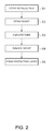
- FIG. 2 is a flowchart showing a manufacturing step of a polarization element according to a first embodiment.
- FIGS. 3A to 3E are views showing a manufacturing step of a polarization element according to a first embodiment.
- FIGS. 4A to 4E are views showing a manufacturing step of a polarization element according to a first embodiment.
- FIG. 5 is a view showing a crystalline structure of a protecting layer.
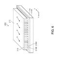
- FIG. 6 is a view showing a polarization element of the related art.
- FIG. 7 is a schematic configuration view showing a projector according to a second embodiment.
- FIG. 8 is a schematic configuration view showing an electronic device according to a third embodiment.
- FIG. 1A is a plane view showing the polarization element 100 of the embodiment
- FIG. 1B is a cross-sectional view taken along a line A-A′ of FIG. 1A and an explanatory diagram of an operation of the polarization element
- FIG. 1C is a cross-sectional view taken along a line B-B′ of FIG. 1A
- FIG. 1D is a cross-sectional view taken along a line C-C′ of FIG. 1A .
- the polarization element 100 is a light reflective polarization element, and includes a substrate 111 A, a wire grid polarization layer 118 formed on a ground layer 114 which covers a surface 111 B of the substrate 111 A, and a protecting layer 113 which is provided on the surface 111 B of the substrate 111 A through the wire grid polarization layer 118 .
- the substrate 111 A is formed of a transparent substrate such as glass, quartz, and plastic, and when the polarization element 100 is a reflective type, an opaque substrate such as a metallic substrate or a ceramic substrate may be used.
- the ground layer 114 is formed on the surface 111 B of the substrate 111 A as necessary, and can be formed by a silicon oxide film or an aluminum oxide film, for example.
- the ground layer 114 includes a function of preventing damage to the substrate 111 A due to etching or the like, and a function of improving adhesiveness of metallic thin lines 118 A with respect to the substrate 111 A, when performing a pattern formation of the metallic thin lines 118 A by etching.
- the ground layer 114 may be formed by a light reflective metallic material.
- the wire grid polarization layer 118 includes the plurality of metallic thin lines 118 A which are disposed in a striped manner with predetermined intervals.
- the wire grid polarization layer 118 is provided on the ground layer 114 .
- the plurality of metallic thin lines 118 A is formed to have a striped pattern in a plan view. For example, a width L of the metallic thin line 118 A is about 70 nm, a height H of the metallic thin line 118 A is about 150 nm, and a space S between the two metallic thin lines 118 A which are adjacent to each other is about 70 nm.
- the height H is set to be equal to or less than 150 nm.
- a ratio L/S defined with the width L and the space S of the metallic thin line 118 A is an important parameter for determining optical properties of the polarization element 100 .
- polarization selection is performed depending on polarization directions of light incident to the polarization element 100 .
- linear polarized light Et including a polarizing axis in a direction perpendicular to an extending direction (X axis direction of FIG.
- the polarization element 100 of the embodiment includes a reflective axis which is parallel to the extending direction of the metallic thin line 118 A and a transmission axis with a direction (Y axis direction of FIG. 1A ) perpendicular to the reflective axis.
- an end portion 120 of the metallic thin line 118 A has a forward tapered shape.
- a portion with the exception of the end portion 120 from the metallic thin line 118 A is referred to as a flat portion 119 of the metallic thin line 118 A.
- An effective region to be used as the polarization element 100 is a region in which the flat portion 119 is formed on the metallic thin line 118 A, and the end portion 120 of the metallic thin line 118 A is formed outside the effective region to be used.
- the protecting layer 113 is provided on the plurality of metallic thin lines 118 A.
- the protecting layer 113 is a dielectric layer which is formed of a dielectric material such as SiO 2 or MgF 2 .
- the protecting layer 113 is formed with an oblique film forming method, and includes a needle-like crystalline structure which is obliquely oriented (see FIG. 5 ).
- the protecting layer 113 extends from the upper portion of the plurality of metallic thin lines 118 A, that is, the upper surface of the flat portion 119 , to the surface 111 B of the substrate 111 A, through each end portion of the plurality of metallic thin lines 118 A.
- the protecting layer 113 is provided on the upper surface of the end portion 120 and also in a region of the surface of the ground layer 114 that leads to the end portion 120 . Further, as shown in FIGS. 1A , 1 B, and 1 D, the protecting layer 113 is also provided on an upper side of a cavity portion 118 B.
- a space between two metallic thin lines 118 A which are adjacent to each other among the plurality of metallic thin lines 118 A is set as the cavity portion 118 B which is surrounded by the two metallic thin lines 118 A which are adjacent to each other, the substrate 111 A (ground layer 114 ), and the protecting layer 113 .
- the plurality of metallic thin lines 118 A and the plurality of cavity portions 118 B are sealed by the protecting layer 113 and the substrate 111 A (ground layer 114 ). According to this, since oxygen is not supplied to the inside of the cavity portion 118 B from the outside of the cavity portion 118 B, when the metallic thin lines 118 A are exposed to a high-temperature environment, although it is oxidized only initially, the oxidization stops with the oxygen depletion. Accordingly, the oxidization of the metallic thin lines 118 A is not likely to occur when the metallic thin lines 118 A are exposed to the high-temperature environment and thus, it is possible to provide a polarization element with superior high-temperature reliability in which the property degradation is suppressed.
- the plurality of metallic thin lines 118 A and the plurality of cavity portions 118 B it is not necessary for the plurality of metallic thin lines 118 A and the plurality of cavity portions 118 B to be sealed by the protecting layer 113 and the substrate 111 A (ground layer 114 ). As long as the cavity portion 118 B is surrounded by the two metallic thin lines 118 A which are adjacent to each other, the substrate 111 A (ground layer 114 ), and the protecting layer 113 so that the supply of the oxygen to the cavity portions 118 B is sufficiently suppressed, the process of the oxidization of the metallic thin lines 118 A is slowed down to obtain an effect of suppressing the property degradation.
- the oxygen concentration of the cavity portions 118 B is maintained to be lower than the oxygen concentration in the outside of the space formed by the protecting layer 113 and the substrate 111 A (ground layer 114 ).
- gas such as an inert gas for example, argon or nitrogen may be hermetically filled in the cavity portion 118 B.
- An amount of the hermetically filled gas is not particularly limited, and may be in a state closer to a full vacuum state.
- the gas such as the inert gas is hermetically filled in the cavity portion 118 B, it is possible to suppress the oxygen concentration of the cavity portion 118 B to be low, without keeping the atmospheric pressure of the inside of the cavity portion 118 B in a lower state compared to the atmospheric pressure of the outside of the cavity portion 118 B. Accordingly, damage to protecting layer 113 due to the difference in atmospheric pressure between inside and outside of the cavity portion 118 B is suppressed and thus, it is possible to provide a polarization element with superior high-temperature reliability in which the property degradation is suppressed.
- the polarization element 100 of the embodiment it is possible to prevent the oxygen from being supplied from the outside of the cavity portion 118 B to the inside of the cavity portion 118 B.
- FIG. 2 is a flowchart showing a manufacturing step of the polarization element 100
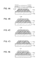
- FIGS. 3A to 3E are schematic views showing the manufacturing step of the polarization element and are cross-sectional views taken along lines A-A′ of FIG. 1A
- FIGS. 4A to 4E are schematic views showing the manufacturing step of the polarization element 100 and are cross-sectional views taken along lines B-B′ of FIG. 1A .
- a silicon oxide film is formed on the surface 111 B of the substrate 111 A which is formed of a translucent material such as glass, quartz, or plastic, by a vapor-deposition method such as a sputtering method or the like, to be set as the ground layer 114 .
- a vapor-deposition method such as a sputtering method or the like
- aluminum (Al) film is formed on the ground layer 114 using the vapor-deposition method such as the sputtering method to form a metallic film 112 a.
- the metallic film 112 a can be formed on the surface 111 B of the substrate 111 A and at the same time, the end portion of the metallic film 112 a can have a forward tapered shape.
- any of gold, copper, palladium, platinum, rhodium, silicon, nickel, cobalt, manganese, iron, chrome, titanium, ruthenium, niobium, neodymium, ytterbium, yttrium, thallium, molybdenum, indium, bismuth, and an alloy thereof, may be used.
- an interference exposure method (dual beam interference exposure, in the embodiment) which is capable of forming a fine striped pattern equal to or less than a wavelength of visible light, is used. After performing such exposure, by performing baking (PEB: Post Exposure Bake) and extracting the exposure portion of the resist film by the etching, the resist 115 a having a pattern shown in FIGS. 3B and 4B can be formed.
- PEB Post Exposure Bake
- a pattern forming step S 3 as shown in FIGS. 3C and 4C , the metallic film 112 a is etched with the formed resist 115 a as a mask.
- the dielectric material is obliquely vapor-deposited so as to cover the upper surface of the metallic thin lines 118 A and the upper side of the cavity portions 118 B.
- the dielectric material is obliquely vapor-deposited from a direction which intersects with the extending direction of the metallic thin lines 118 A and which is oblique with respect to the normal direction of the surface 111 B of the substrate 111 A.
- the dielectric material is obliquely vapor-deposited from the Y axis direction when seen the substrate 111 A from a plan view.
- the protecting layer 113 can be easily formed on the wire grid polarization layer 118 so that the cavity portion 118 B is surrounded by the two metallic thin lines 118 A which are adjacent to each other, the ground layer 114 , and the protecting layer 113 .
- cavity portions 218 B are provided on the end portions of the metallic thin lines 218 A, and the cavity portions 218 B are formed as spaces which are opened to the outside of the cavity portions 218 B.
- the oxidization of the metallic thin lines 218 A when the polarization element 100 is exposed to a high-temperature environment is difficult to suppress.
- the protecting layer 113 is continuously guided to the surface 111 B of the substrate 111 A from the upper portion of the plurality of metallic thin lines (protrusions) 118 A and the upper side of the plurality of cavity portions 118 B, through the end portion 120 having a forward tapered shape.
- the cavity portion 118 B can be reliably sealed by the two metallic thin lines 118 A which are adjacent to each other, the ground layer 114 , and the protecting layer 113 .
- atmosphere gas in a deposition apparatus is hermetically filled by the protecting layer 113 in a state of being hermetically filled in the cavity portions 118 B when forming a film.
- atmosphere gas is argon
- argon may be hermetically filled or the air may be hermetically filled.
- the inside of the deposition apparatus is in a reduced pressure state
- the inside of the cavity portions 118 B is also set to be in a pressure reduction state.
- the cavity portion 118 B in which the gas such as the inactive gas is hermetically filled, is formed between the metallic thin lines 118 A which are adjacent to each other.
- the polarization element 100 in which the plurality of metallic thin lines 118 A and the plurality of cavity portions 118 B in the space formed by the protecting layer 113 and the substrate 111 A (ground layer 114 ) are provided.
- FIG. 7 is a schematic configuration view showing main parts of a projector 800 including the polarization element according to the first embodiment.
- the projector 800 of the embodiment is a liquid crystal projector with a liquid crystal light modulating device used as a light modulating device.
- the projector 800 includes a light source 810 , a dichroic mirror 813 , a dichroic mirror 814 , a reflecting mirror 815 , a reflecting mirror 816 , a reflecting mirror 817 , a light entering lens 818 , a relay lens 819 , a light emitting lens 820 , a liquid crystal modulating device for red light 822 , a liquid crystal modulating device for green light 823 , a liquid crystal modulating device for blue light 824 , a cross dichroic prism 825 , a projecting lens 826 , an entering side polarization element 831 , an entering side polarization element 832 , an entering side polarization element 833 , an emitting side polarization element 834 , an emitting side polarization element 835 , and an emitting side polarization element 836 .
- the dichroic mirror 813 transmits red light included in white light from the light source 810 , and reflects blue light and green light.
- the cross dichroic prism 825 is obtained by joining four right-angled prisms, and a dielectric multilayer which reflects red light and a dielectric multilayer which reflects blue light are formed in an X-shape on the interfacial surfaces thereof.
- the three colored lights are combined by the dielectric multilayer and light for showing a color image is formed.
- the combined light is projected on a screen 827 by the projecting lens 826 which is an optical system for projecting, and an image is enlarged and displayed.
- the polarization element according to the first embodiment shown in FIGS. 1A to 1D is employed as the polarization elements 831 to 836 .
- the polarization elements 831 to 836 are configured by the polarization element including the wire grid polarization layer 118 formed of the metallic film with high light resistance and heat resistance.
- the three plate type projector has been described as an example; however, the polarization element according to the first embodiment can be applied to a projection type display apparatus or a direct-view type display apparatus of a single plate type.
- FIG. 8 is a perspective configuration view of a mobile phone which is an example of an electronic device which includes the liquid crystal device including the polarization element according to the first embodiment as a display unit.
- a mobile phone 1300 includes the liquid crystal device as a small-sized display unit 1301 , and includes a plurality of manual operation buttons 1302 , an ear piece 1303 , and a mouthpiece 1304 .
- the liquid crystal device is not limited to being used in the mobile phone, and can suitably be used as an image display unit such as an electronic book, a personal computer, a digital still camera, a liquid crystal television, a view finder type or a monitor direct-view type video tape recorder, a car navigation system, a pager, an electronic notebook, a calculator, a word processor, a workstation, a video phone, a POS terminal, a device including a touch panel, or the like, and it is possible to obtain a high brightness, a high contrast, transmission display and reflection display of a wide viewing angle, for any of the electronic devices.
- an image display unit such as an electronic book, a personal computer, a digital still camera, a liquid crystal television, a view finder type or a monitor direct-view type video tape recorder, a car navigation system, a pager, an electronic notebook, a calculator, a word processor, a workstation, a video phone, a POS terminal, a device including a touch panel, or
Landscapes
- Physics & Mathematics (AREA)
- General Physics & Mathematics (AREA)
- Optics & Photonics (AREA)
- Polarising Elements (AREA)
- Liquid Crystal (AREA)
- Projection Apparatus (AREA)
Abstract
Description
- 1. Technical Field
- The present invention relates to a polarization separating element which is generally called a wire grid polarization element.
- 2. Related Art
- A wire grid polarization element has a configuration in that a grid formed of metal is laid on a transparent substrate. The biggest property of the wire grid polarization element is that the pitch of the grid is sufficiently shorter than a wavelength being used.
- Since the wire grid polarization element is configured of only inorganic materials, degradation due to heat does not frequently occur, compared to a polarization element using organic materials. However, since a projector obtains a higher brightness year on year, high temperature reliability of an inorganic polarization element which is disposed on a light path thereof becomes a problem due to an increase in temperatures.
- As a result of an investigation, it is determined that degradation in an optical property measured when the inorganic polarization element is held at a high temperature, is due to a thermally-oxidized film which grows on a surface of the metallic grid (in general, aluminum is used).
- As a technology for protecting the metallic grid, JP-A-2007-17762 discloses that a protecting layer is provided on the metallic grid with an obliquely film-forming method. According to JP-A-2007-17762, a cavity portion is formed by two metallic thin lines which are adjacent to each other, a substrate, and a protecting layer.
- However, when the protecting layer is formed with a method disclosed in JP-A-2007-17762, since an end portion of the cavity portion is not covered by the protecting layer, oxygen is supplied to the inside of the cavity portion from the end portion of the cavity portion. Thus, there is a concern that the metallic grid is oxidized in a high-temperature environment.
- An advantage of some aspects of the invention is to solve at least a part of the problems described above, and the invention can be implemented as the following forms or application examples.
- This application example is directed to a polarization element including: a plurality of metallic thin lines that extend in one direction on one surface of a substrate; a protecting layer that is provided on the plurality of metallic thin lines; and a cavity portion that is surrounded by two metallic thin lines which are adjacent to each other among the plurality of metallic thin lines, the substrate, and the protecting layer, wherein each end portion of the plurality of metallic thin layers has a forward tapered shape in a cross-section parallel to the one direction, and the protecting layer extends from the upper portion of the plurality of metallic thin lines to the one surface of the substrate through each end portion of the plurality of metallic thin lines.
- According to this application example, each end portion of the plurality of metallic thin lines has a forward tapered shape in a cross-section parallel to the extending direction, and the protecting layer extends from the upper portion of the plurality of metallic thin lines to the one surface of the substrate through each end portion of the plurality of metallic thin lines. Thus, the space between two metallic thin lines which are adjacent to each other among the plurality of metallic thin lines becomes the cavity portion which is surrounded by the two metallic thin lines which are adjacent to each other, the substrate, and the protecting layer. Since oxygen is difficult to supply to the inside of the cavity portion from the outside of the cavity portion, when the metallic thin lines are exposed to a high-temperature environment, although they are initially oxidized, it is gradually less likely to be oxidized. Accordingly, metallic thin lines are not likely to be oxidized when exposed to a high-temperature environment and it is possible to provide a polarization element with superior high-temperature reliability in which the property degradation is suppressed.
- This application example is directed to the polarization element according to the application example described above, wherein an oxygen concentration of the cavity portion is lower than the oxygen concentration outside the cavity portion.
- According to this application example, since an amount of oxygen in the cavity is small, initial oxidization of metallic thin lines is not likely to occur, when the metallic thin lines are exposed to a high-temperature environment. Thus, it is possible to provide a polarization element with superior high-temperature reliability in which the property degradation is suppressed.
- This application example is directed to the polarization element according to the application example described above, wherein an inert gas is hermetically filled in the cavity portion.
- According to this application example, it is possible to set the oxygen concentration in the cavity to be low, without keeping atmospheric pressure in the cavity in a lower state compared to atmospheric pressure outside the cavity. Accordingly, damage to the protecting layer due to the difference in atmospheric pressure between the inside and outside a cavity is suppressed and thus, it is possible to provide a polarization element with superior high-temperature reliability in which the property degradation is suppressed.
- This application example is directed to the polarization element according to the application example described above, wherein the plurality of metallic thin lines and the plurality of cavity portions are sealed by the protecting layer and the substrate.
- According to this application example, since the plurality of metallic thin lines and the plurality of cavity portions are sealed by the protecting layer and the substrate, oxygen is not supplied to the inside of the cavity portion from the outside of the cavity portion. Thus, when the metallic thin lines are exposed to a high-temperature environment, although they are oxidized only initially, the oxidization stops with the oxygen depletion. Accordingly, oxidization of metallic thin lines is not likely to occur when the metallic thin lines are exposed to a high-temperature environment and thus, it is possible to provide a polarization element with superior high-temperature reliability in which the property degradation is suppressed.
- This application example is directed to a method of manufacturing a polarization element including a plurality of metallic thin lines that extend in one direction on one surface of a substrate, a protecting layer that is provided on the plurality of metallic thin lines, and a cavity portion that is surrounded by two metallic thin lines which are adjacent to each other among the plurality of metallic thin lines, the substrate, and the protecting layer, wherein each end portion of the plurality of metallic thin lines has a forward tapered shape in a cross-section parallel to the one direction. The method includes: forming a metallic film on the one surface of the substrate; forming a striped resist pattern on the metallic film; etching the metallic film with the striped resist pattern as a mask to form the plurality of metallic thin lines; and forming the protecting layer on the plurality of metallic thin lines, wherein, in the forming of the metallic film, the metallic film is formed so that an end portion of the metallic film has a forward tapered shape, and in the forming of the protecting layer, the protecting layer is formed so that the cavity portion surrounded by the two metallic thin lines, the substrate and the protecting layer is formed.
- According to this application example, the forming of the metallic film and the forward tapered shape process of the end portion of the metallic film are performed at the same time. In addition, since each end portion of the plurality of metallic thin lines has a forward tapered shape, the protecting layer is continuously guided to the one surface of the substrate from the upper portion of the plurality of metallic thin lines and upper side of the plurality of cavity portions through the forward tapered shaped portion. Accordingly, it is easy to set a space between two metallic thin lines which are adjacent to each other among the plurality of metallic thin lines as the cavity portion surrounded by the two metallic thin lines which are adjacent to each other, the substrate, and the protecting layer. Thus, it is possible to easily form a polarization element with superior high-temperature reliability in which oxidization of metallic thin lines is not likely to occur when the metallic thin lines are exposed to a high-temperature environment, and the property degradation is suppressed, without undergoing complicated processes.
- This application example is directed to the method of manufacturing a polarization element according to the application example described above, wherein in the forming of the protecting layer, the protecting layer is obliquely vapor-deposited from a direction which intersects with the one direction and which is oblique with respect to a normal line of the one surface of the substrate.
- According to this application example, it is easy to set a space between two metallic thin lines which are adjacent to each other among the plurality of metallic thin lines as the cavity portion surrounded by the two metallic thin lines which are adjacent to each other, the substrate, and the protecting layer.
- This application example is directed to the method of manufacturing a polarization element according to the application example described above, wherein in the forming of the metallic film, the metallic film is vapor-deposited on the one surface of the substrate with a mask that is provided between a film source and the substrate so that the end portion of the metallic film has a forward tapered shape.
- According to this application example, it is easily possible that the end portion of the metallic film has a forward tapered shape.
- This application example is directed to a projector including the polarization element according to any of the application examples described above.
- According to this application example, it is possible to realize a projector including a polarization optical system which is excellent in display quality and reliability.
- This application example is directed to an electronic device including the polarization element according to any of the application examples described above.
- According to this application example, it is possible to realize an electronic device including a polarization optical system which is excellent in display quality and reliability.
- The invention will be described with reference to the accompanying drawings, wherein like numbers reference like elements.
-
FIGS. 1A to 1D are views showing a polarization element according to a first embodiment. -
FIG. 2 is a flowchart showing a manufacturing step of a polarization element according to a first embodiment. -
FIGS. 3A to 3E are views showing a manufacturing step of a polarization element according to a first embodiment. -
FIGS. 4A to 4E are views showing a manufacturing step of a polarization element according to a first embodiment. -
FIG. 5 is a view showing a crystalline structure of a protecting layer. -
FIG. 6 is a view showing a polarization element of the related art. -
FIG. 7 is a schematic configuration view showing a projector according to a second embodiment. -
FIG. 8 is a schematic configuration view showing an electronic device according to a third embodiment. - Hereinafter, the embodiments of the invention will be described with reference to the drawings. The drawings used in the description below are appropriately enlarged and reduced in size so that each of members is recognizable.
- First, a
polarization element 100 of the embodiment will be described with reference toFIGS. 1A to 1D . Herein,FIG. 1A is a plane view showing thepolarization element 100 of the embodiment,FIG. 1B is a cross-sectional view taken along a line A-A′ ofFIG. 1A and an explanatory diagram of an operation of the polarization element,FIG. 1C is a cross-sectional view taken along a line B-B′ ofFIG. 1A , andFIG. 1D is a cross-sectional view taken along a line C-C′ ofFIG. 1A . - As shown in
FIGS. 1A to 1D , thepolarization element 100 is a light reflective polarization element, and includes asubstrate 111A, a wiregrid polarization layer 118 formed on aground layer 114 which covers asurface 111B of thesubstrate 111A, and aprotecting layer 113 which is provided on thesurface 111B of thesubstrate 111A through the wiregrid polarization layer 118. - The
substrate 111A is formed of a transparent substrate such as glass, quartz, and plastic, and when thepolarization element 100 is a reflective type, an opaque substrate such as a metallic substrate or a ceramic substrate may be used. - In addition, the
ground layer 114 is formed on thesurface 111B of thesubstrate 111A as necessary, and can be formed by a silicon oxide film or an aluminum oxide film, for example. Theground layer 114 includes a function of preventing damage to thesubstrate 111A due to etching or the like, and a function of improving adhesiveness of metallicthin lines 118A with respect to thesubstrate 111A, when performing a pattern formation of the metallicthin lines 118A by etching. In addition, when forming a reflective polarization element as thepolarization element 100, theground layer 114 may be formed by a light reflective metallic material. - The wire
grid polarization layer 118 includes the plurality of metallicthin lines 118A which are disposed in a striped manner with predetermined intervals. The wiregrid polarization layer 118 is provided on theground layer 114. The plurality of metallicthin lines 118A is formed to have a striped pattern in a plan view. For example, a width L of the metallicthin line 118A is about 70 nm, a height H of the metallicthin line 118A is about 150 nm, and a space S between the two metallicthin lines 118A which are adjacent to each other is about 70 nm. The height H is set to be equal to or less than 150 nm. - Herein, a ratio L/S defined with the width L and the space S of the metallic
thin line 118A is an important parameter for determining optical properties of thepolarization element 100. As shown inFIG. 1B , since the plurality of metallicthin lines 118A which is formed with a narrower pitch (about 140 nm) than a wavelength of visible light are provided, polarization selection is performed depending on polarization directions of light incident to thepolarization element 100. In detail, linear polarized light Et including a polarizing axis in a direction perpendicular to an extending direction (X axis direction ofFIG. 1A ) of the metallicthin line 118A is transmitted, however linear polarized light Er including a polarizing axis in a direction parallel to the extending direction of the metallicthin line 118A is reflected. Accordingly, thepolarization element 100 of the embodiment includes a reflective axis which is parallel to the extending direction of the metallicthin line 118A and a transmission axis with a direction (Y axis direction ofFIG. 1A ) perpendicular to the reflective axis. - As shown in
FIG. 1C , in a cross-section parallel to the X axis direction, anend portion 120 of the metallicthin line 118A has a forward tapered shape. For the sake of convenience, in the present specification, a portion with the exception of theend portion 120 from the metallicthin line 118A is referred to as aflat portion 119 of the metallicthin line 118A. An effective region to be used as thepolarization element 100 is a region in which theflat portion 119 is formed on the metallicthin line 118A, and theend portion 120 of the metallicthin line 118A is formed outside the effective region to be used. - The protecting
layer 113 is provided on the plurality of metallicthin lines 118A. The protectinglayer 113 is a dielectric layer which is formed of a dielectric material such as SiO2 or MgF2. As will be described later, the protectinglayer 113 is formed with an oblique film forming method, and includes a needle-like crystalline structure which is obliquely oriented (seeFIG. 5 ). - As shown in
FIGS. 1A to 1D , the protectinglayer 113 extends from the upper portion of the plurality of metallicthin lines 118A, that is, the upper surface of theflat portion 119, to thesurface 111B of thesubstrate 111A, through each end portion of the plurality of metallicthin lines 118A. As described above, the protectinglayer 113 is provided on the upper surface of theend portion 120 and also in a region of the surface of theground layer 114 that leads to theend portion 120. Further, as shown inFIGS. 1A , 1B, and 1D, the protectinglayer 113 is also provided on an upper side of acavity portion 118B. Thus, a space between two metallicthin lines 118A which are adjacent to each other among the plurality of metallicthin lines 118A is set as thecavity portion 118B which is surrounded by the two metallicthin lines 118A which are adjacent to each other, thesubstrate 111A (ground layer 114), and theprotecting layer 113. - It is preferable for the plurality of metallic
thin lines 118A and the plurality ofcavity portions 118B to be sealed by the protectinglayer 113 and thesubstrate 111A (ground layer 114). According to this, since oxygen is not supplied to the inside of thecavity portion 118B from the outside of thecavity portion 118B, when the metallicthin lines 118A are exposed to a high-temperature environment, although it is oxidized only initially, the oxidization stops with the oxygen depletion. Accordingly, the oxidization of the metallicthin lines 118A is not likely to occur when the metallicthin lines 118A are exposed to the high-temperature environment and thus, it is possible to provide a polarization element with superior high-temperature reliability in which the property degradation is suppressed. - In addition, it is not necessary for the plurality of metallic
thin lines 118A and the plurality ofcavity portions 118B to be sealed by the protectinglayer 113 and thesubstrate 111A (ground layer 114). As long as thecavity portion 118B is surrounded by the two metallicthin lines 118A which are adjacent to each other, thesubstrate 111A (ground layer 114), and theprotecting layer 113 so that the supply of the oxygen to thecavity portions 118B is sufficiently suppressed, the process of the oxidization of the metallicthin lines 118A is slowed down to obtain an effect of suppressing the property degradation. - It is preferable that the oxygen concentration of the
cavity portions 118B is maintained to be lower than the oxygen concentration in the outside of the space formed by the protectinglayer 113 and thesubstrate 111A (ground layer 114). For this, gas such as an inert gas for example, argon or nitrogen may be hermetically filled in thecavity portion 118B. An amount of the hermetically filled gas is not particularly limited, and may be in a state closer to a full vacuum state. However, when the gas such as the inert gas is hermetically filled in thecavity portion 118B, it is possible to suppress the oxygen concentration of thecavity portion 118B to be low, without keeping the atmospheric pressure of the inside of thecavity portion 118B in a lower state compared to the atmospheric pressure of the outside of thecavity portion 118B. Accordingly, damage to protectinglayer 113 due to the difference in atmospheric pressure between inside and outside of thecavity portion 118B is suppressed and thus, it is possible to provide a polarization element with superior high-temperature reliability in which the property degradation is suppressed. - As described above, in the
polarization element 100 of the embodiment, it is possible to prevent the oxygen from being supplied from the outside of thecavity portion 118B to the inside of thecavity portion 118B. Alternatively, it is possible to suppress the amount of the oxygen supplied to the inside of thecavity portion 118B to be an extremely small amount, by making the oxygen be difficult to supply from the outside of thecavity portion 118B to the inside of thecavity portion 118B. Accordingly, the oxidization of the metallicthin lines 118A when thepolarization element 100 is exposed to a high-temperature environment can be suppressed. Thus, it is possible to improve the high-temperature reliability of thepolarization element 100. - Next, a method of manufacturing the
polarization element 100 described above will be described with reference toFIGS. 2 to 4E . Herein,FIG. 2 is a flowchart showing a manufacturing step of thepolarization element 100, andFIGS. 3A to 3E are schematic views showing the manufacturing step of the polarization element and are cross-sectional views taken along lines A-A′ ofFIG. 1A .FIGS. 4A to 4E are schematic views showing the manufacturing step of thepolarization element 100 and are cross-sectional views taken along lines B-B′ ofFIG. 1A . - Hereinafter, the method of manufacturing the polarization element will be described with reference to the flowchart of
FIG. 2 . - First, in a metallic film forming step S1, as shown in
FIG. 3A , for example, a silicon oxide film is formed on thesurface 111B of thesubstrate 111A which is formed of a translucent material such as glass, quartz, or plastic, by a vapor-deposition method such as a sputtering method or the like, to be set as theground layer 114. After that, aluminum (Al) film is formed on theground layer 114 using the vapor-deposition method such as the sputtering method to form ametallic film 112 a. - At this time, as shown in
FIG. 4A , by providing amask 116 between a sputtering target (film source) and the substrate, themetallic film 112 a can be formed on thesurface 111B of thesubstrate 111A and at the same time, the end portion of themetallic film 112 a can have a forward tapered shape. - As a metal configuring the
metallic film 112 a, other than aluminum, for example, any of gold, copper, palladium, platinum, rhodium, silicon, nickel, cobalt, manganese, iron, chrome, titanium, ruthenium, niobium, neodymium, ytterbium, yttrium, thallium, molybdenum, indium, bismuth, and an alloy thereof, may be used. - Next, in a resist forming step S2, a resist is applied onto the
metallic film 112 a by a spin coating, and is baked to form a resist film. After that, exposure and developing processing are performed and a resist 115 a with a striped shape in a plan view is formed, as shown inFIGS. 3B and 4B . In detail, laser irradiation is selectively performed with respect to the resist film described above, so as to dispose the resist 115 a to be formed with a striped shape. Since a pitch of the resist 115 a to be formed is 140 nm in the embodiment, an interference exposure method, (dual beam interference exposure, in the embodiment) which is capable of forming a fine striped pattern equal to or less than a wavelength of visible light, is used. After performing such exposure, by performing baking (PEB: Post Exposure Bake) and extracting the exposure portion of the resist film by the etching, the resist 115 a having a pattern shown inFIGS. 3B and 4B can be formed. - Then, in a pattern forming step S3, as shown in
FIGS. 3C and 4C , themetallic film 112 a is etched with the formed resist 115 a as a mask. - Further, in a resist removing step S4, by removing the resist 115 a, the plurality of metallic
thin lines 118A as shown inFIGS. 3D and 4D is formed and the wiregrid polarization layer 118 is formed. - Finally, a protecting layer forming step S5 will be described in detail with reference to
FIG. 3E . As shown by an arrow inFIG. 3E , the dielectric material is obliquely vapor-deposited so as to cover the upper surface of the metallicthin lines 118A and the upper side of thecavity portions 118B. In detail, the dielectric material is obliquely vapor-deposited from a direction which intersects with the extending direction of the metallicthin lines 118A and which is oblique with respect to the normal direction of thesurface 111B of thesubstrate 111A. In the embodiment, the dielectric material is obliquely vapor-deposited from the Y axis direction when seen thesubstrate 111A from a plan view. Accordingly, the protectinglayer 113 can be easily formed on the wiregrid polarization layer 118 so that thecavity portion 118B is surrounded by the two metallicthin lines 118A which are adjacent to each other, theground layer 114, and theprotecting layer 113. - Herein, a
polarization element 200 of the related art is shown inFIG. 6 . In thepolarization element 200, end portions of the metallicthin lines 218A have vertical sectional shapes on the cross-section parallel to the extending direction (X axis direction) of metallicthin lines 218A. In aprotecting layer 213, an upper surface of aflat portion 219 of the metallicthin lines 218A is covered by the protectinglayer 213, to form obliquely from a direction parallel to a Y axis direction ofFIG. 6 , however, the end portions of the metallicthin lines 218A are not covered by the protectinglayer 213. Accordingly, an opening portion ofcavity portions 218B are provided on the end portions of the metallicthin lines 218A, and thecavity portions 218B are formed as spaces which are opened to the outside of thecavity portions 218B. Thus, the oxidization of the metallicthin lines 218A when thepolarization element 100 is exposed to a high-temperature environment is difficult to suppress. - Meanwhile, according to the embodiment, the protecting
layer 113 is continuously guided to thesurface 111B of thesubstrate 111A from the upper portion of the plurality of metallic thin lines (protrusions) 118A and the upper side of the plurality ofcavity portions 118B, through theend portion 120 having a forward tapered shape. Thus, thecavity portion 118B can be reliably sealed by the two metallicthin lines 118A which are adjacent to each other, theground layer 114, and theprotecting layer 113. - At this time, if the vapor-deposition method is used, for example, atmosphere gas in a deposition apparatus is hermetically filled by the protecting
layer 113 in a state of being hermetically filled in thecavity portions 118B when forming a film. Accordingly, if the atmosphere gas is argon, argon may be hermetically filled or the air may be hermetically filled. Further, since the inside of the deposition apparatus is in a reduced pressure state, the inside of thecavity portions 118B is also set to be in a pressure reduction state. As described above, thecavity portion 118B, in which the gas such as the inactive gas is hermetically filled, is formed between the metallicthin lines 118A which are adjacent to each other. - By the steps described above, as shown in
FIGS. 1A to 1D , it is possible to manufacture thepolarization element 100 in which the plurality of metallicthin lines 118A and the plurality ofcavity portions 118B in the space formed by the protectinglayer 113 and thesubstrate 111A (ground layer 114) are provided. - By performing the process described above, it is possible to reliably form the
cavity portion 118B which is surrounded by the two metallicthin lines 118A which are adjacent to each other, thesubstrate 111A, and theprotecting layer 113. Accordingly, it is possible to easily form thepolarization element 100 of a wire grid type, with a good extinction ratio (a transmittance ratio with respect to the polarizing component) and superior high temperature reliability. -
FIG. 7 is a schematic configuration view showing main parts of aprojector 800 including the polarization element according to the first embodiment. Theprojector 800 of the embodiment is a liquid crystal projector with a liquid crystal light modulating device used as a light modulating device. - The
projector 800 includes alight source 810, adichroic mirror 813, adichroic mirror 814, a reflectingmirror 815, a reflectingmirror 816, a reflectingmirror 817, alight entering lens 818, a relay lens 819, alight emitting lens 820, a liquid crystal modulating device forred light 822, a liquid crystal modulating device forgreen light 823, a liquid crystal modulating device forblue light 824, a crossdichroic prism 825, a projectinglens 826, an enteringside polarization element 831, an enteringside polarization element 832, an enteringside polarization element 833, an emittingside polarization element 834, an emittingside polarization element 835, and an emittingside polarization element 836. - The
light source 810 is formed of alamp 811 such as a metal halide, and areflector 812 which reflects light from thelamp 811. As thelight source 810, other than the metal halide, an extra high pressure mercury lamp, a flash mercury lamp, a high pressure mercury lamp, a Deep UV lamp, a xenon lamp, a xenon flash lamp or the like can be used. - The
dichroic mirror 813 transmits red light included in white light from thelight source 810, and reflects blue light and green light. - The transmitted red light is reflected by the reflecting
mirror 817, and enters the liquid crystal light modulating device forred light 822 through the enteringside polarization element 831. In addition, the green light reflected by thedichroic mirror 813 is reflected by thedichroic mirror 814 and enters the liquid crystal modulating device forgreen light 823 through the enteringside polarization element 832. Further, the blue light reflected by thedichroic mirror 813 transmits through thedichroic mirror 814. In order to prevent light loss due to a long light path, alight guiding unit 821 which is formed of a relay lens system including thelight entering lens 818, the relay lens 819, and thelight emitting lens 820, is provided for the blue light. With thelight guiding unit 821, the blue light enters the liquid crystal modulating device forblue light 824 through the enteringside polarization element 833. - Each of the three colored light beams modulated by the
light modulating devices 822 to 824 enters the crossdichroic prism 825 through each of the emittingside polarization elements 834 to 836. The crossdichroic prism 825 is obtained by joining four right-angled prisms, and a dielectric multilayer which reflects red light and a dielectric multilayer which reflects blue light are formed in an X-shape on the interfacial surfaces thereof. The three colored lights are combined by the dielectric multilayer and light for showing a color image is formed. The combined light is projected on ascreen 827 by the projectinglens 826 which is an optical system for projecting, and an image is enlarged and displayed. - Herein, in the projector of the embodiment, the polarization element according to the first embodiment shown in
FIGS. 1A to 1D is employed as thepolarization elements 831 to 836. Since thelight source 810 from thelamp 811 emits light with high energy, there is a concern that the organic material maybe degraded or deformed due to the light with high energy. Therefore, thepolarization elements 831 to 836 are configured by the polarization element including the wiregrid polarization layer 118 formed of the metallic film with high light resistance and heat resistance. - In the embodiment, the three plate type projector has been described as an example; however, the polarization element according to the first embodiment can be applied to a projection type display apparatus or a direct-view type display apparatus of a single plate type.
-
FIG. 8 is a perspective configuration view of a mobile phone which is an example of an electronic device which includes the liquid crystal device including the polarization element according to the first embodiment as a display unit. A mobile phone 1300 includes the liquid crystal device as a small-sized display unit 1301, and includes a plurality of manual operation buttons 1302, an ear piece 1303, and a mouthpiece 1304. - The liquid crystal device is not limited to being used in the mobile phone, and can suitably be used as an image display unit such as an electronic book, a personal computer, a digital still camera, a liquid crystal television, a view finder type or a monitor direct-view type video tape recorder, a car navigation system, a pager, an electronic notebook, a calculator, a word processor, a workstation, a video phone, a POS terminal, a device including a touch panel, or the like, and it is possible to obtain a high brightness, a high contrast, transmission display and reflection display of a wide viewing angle, for any of the electronic devices.
- The entire disclosure of Japanese Patent Application No. 2012-066922, filed on Mar. 23, 2012 is expressly incorporated by reference herein.
Claims (15)
Applications Claiming Priority (2)
| Application Number | Priority Date | Filing Date | Title |
|---|---|---|---|
| JP2012-066922 | 2012-03-23 | ||
| JP2012066922A JP5796522B2 (en) | 2012-03-23 | 2012-03-23 | Polarizing element and manufacturing method of polarizing element |
Publications (2)
| Publication Number | Publication Date |
|---|---|
| US20130250412A1 true US20130250412A1 (en) | 2013-09-26 |
| US9086543B2 US9086543B2 (en) | 2015-07-21 |
Family
ID=49192746
Family Applications (1)
| Application Number | Title | Priority Date | Filing Date |
|---|---|---|---|
| US13/839,241 Active 2033-10-16 US9086543B2 (en) | 2012-03-23 | 2013-03-15 | Polarization element and method of manufacturing polarization element |
Country Status (3)
| Country | Link |
|---|---|
| US (1) | US9086543B2 (en) |
| JP (1) | JP5796522B2 (en) |
| CN (1) | CN103323901B (en) |
Cited By (8)
| Publication number | Priority date | Publication date | Assignee | Title |
|---|---|---|---|---|
| US9310637B2 (en) * | 2012-08-31 | 2016-04-12 | Panasonic Intellectual Property Management Co., Ltd. | Liquid crystal display device |
| US20170045751A1 (en) * | 2014-04-22 | 2017-02-16 | Politecnico Di Milano | Interactive Device for the Selective Control of Electromagnetic Radiation |
| US20180267357A1 (en) * | 2017-03-14 | 2018-09-20 | Seiko Epson Corporation | Wire grid polarization element and projection type display apparatus |
| US20190049786A1 (en) * | 2017-08-08 | 2019-02-14 | Samsung Display Co., Ltd. | Display apparatus and method for manufacturing the same |
| US20190129263A1 (en) * | 2017-10-30 | 2019-05-02 | Seiko Epson Corporation | Electro-optical device and electronic apparatus |
| US10859743B2 (en) | 2017-09-26 | 2020-12-08 | Dexerials Corporation | Polarizing element, polarizing element manufacturing method, and optical device |
| US10962698B2 (en) * | 2015-01-08 | 2021-03-30 | Dexerials Corporation | Inorganic polarizing plate |
| US20230411573A1 (en) * | 2021-07-16 | 2023-12-21 | Fujian Jing'an Optoelectronics Co., Ltd. | Polarizer, light emitting device, and light emitting apparatus |
Families Citing this family (11)
| Publication number | Priority date | Publication date | Assignee | Title |
|---|---|---|---|---|
| CN104459866A (en) * | 2014-12-30 | 2015-03-25 | 京东方科技集团股份有限公司 | Round polarizing film, manufacturing method of round polarizing film and display panel |
| KR102319565B1 (en) | 2015-01-08 | 2021-11-01 | 삼성디스플레이 주식회사 | Liquid crystal display |
| KR102581143B1 (en) * | 2016-08-18 | 2023-09-21 | 삼성디스플레이 주식회사 | Display device |
| US20200089048A1 (en) * | 2016-12-06 | 2020-03-19 | Scivax Corporation | Optical member, liquid crystal panel using the optical member, and manufacturing methods therefor |
| JP6988079B2 (en) * | 2016-12-14 | 2022-01-05 | ウシオ電機株式会社 | Method for manufacturing grid polarizing element and grid polarizing element for ultraviolet rays |
| CN107544180A (en) * | 2017-09-26 | 2018-01-05 | 京东方科技集团股份有限公司 | Light emitting diode, backlight module and liquid crystal display device |
| CN108181678A (en) * | 2017-12-29 | 2018-06-19 | 深圳市华星光电技术有限公司 | Metal polaroid and the display device for including the metal polaroid |
| JP2018189980A (en) * | 2018-07-19 | 2018-11-29 | デクセリアルズ株式会社 | Polarizing plate |
| JP7226936B2 (en) | 2018-07-26 | 2023-02-21 | デクセリアルズ株式会社 | Polarizing plate and optical equipment |
| CN110618556A (en) * | 2019-09-27 | 2019-12-27 | 维沃移动通信有限公司 | Display module and electronic equipment |
| JP7219735B2 (en) * | 2020-03-26 | 2023-02-08 | デクセリアルズ株式会社 | Polarizing plate, manufacturing method thereof, and optical device |
Citations (2)
| Publication number | Priority date | Publication date | Assignee | Title |
|---|---|---|---|---|
| US20050128587A1 (en) * | 2003-12-05 | 2005-06-16 | Enplas Corporation | Wire grid polarizer |
| US20100225832A1 (en) * | 2009-03-06 | 2010-09-09 | Seiko Epson Corporation | Polarizing element and method for manufacturing the same, projection type display, liquid crystal device, and electronic apparatus |
Family Cites Families (5)
| Publication number | Priority date | Publication date | Assignee | Title |
|---|---|---|---|---|
| JPS6066203A (en) * | 1983-09-22 | 1985-04-16 | Matsushita Electric Ind Co Ltd | Polarizing element |
| JP2004045672A (en) * | 2002-07-11 | 2004-02-12 | Canon Inc | Polarization separation element and optical system using the same |
| JP4497041B2 (en) | 2005-07-08 | 2010-07-07 | セイコーエプソン株式会社 | Manufacturing method of wire grid polarizer |
| JP5096735B2 (en) * | 2006-12-05 | 2012-12-12 | Jx日鉱日石エネルギー株式会社 | Wire grid polarizer and method for manufacturing the same, and retardation film and liquid crystal display device using the same |
| JP2009086040A (en) * | 2007-09-27 | 2009-04-23 | Nippon Zeon Co Ltd | Grid polarizing film and manufacturing method thereof |
-
2012
- 2012-03-23 JP JP2012066922A patent/JP5796522B2/en active Active
-
2013
- 2013-03-15 US US13/839,241 patent/US9086543B2/en active Active
- 2013-03-21 CN CN201310092317.8A patent/CN103323901B/en active Active
Patent Citations (2)
| Publication number | Priority date | Publication date | Assignee | Title |
|---|---|---|---|---|
| US20050128587A1 (en) * | 2003-12-05 | 2005-06-16 | Enplas Corporation | Wire grid polarizer |
| US20100225832A1 (en) * | 2009-03-06 | 2010-09-09 | Seiko Epson Corporation | Polarizing element and method for manufacturing the same, projection type display, liquid crystal device, and electronic apparatus |
Cited By (12)
| Publication number | Priority date | Publication date | Assignee | Title |
|---|---|---|---|---|
| US9310637B2 (en) * | 2012-08-31 | 2016-04-12 | Panasonic Intellectual Property Management Co., Ltd. | Liquid crystal display device |
| US20170045751A1 (en) * | 2014-04-22 | 2017-02-16 | Politecnico Di Milano | Interactive Device for the Selective Control of Electromagnetic Radiation |
| US10962698B2 (en) * | 2015-01-08 | 2021-03-30 | Dexerials Corporation | Inorganic polarizing plate |
| US20180267357A1 (en) * | 2017-03-14 | 2018-09-20 | Seiko Epson Corporation | Wire grid polarization element and projection type display apparatus |
| US10503005B2 (en) * | 2017-03-14 | 2019-12-10 | Seiko Epson Corporation | Wire grid polarization element and projection type display apparatus |
| US20190049786A1 (en) * | 2017-08-08 | 2019-02-14 | Samsung Display Co., Ltd. | Display apparatus and method for manufacturing the same |
| US10690957B2 (en) * | 2017-08-08 | 2020-06-23 | Samsung Display Co., Ltd. | Display apparatus and method for manufacturing the same |
| US10859743B2 (en) | 2017-09-26 | 2020-12-08 | Dexerials Corporation | Polarizing element, polarizing element manufacturing method, and optical device |
| US11754766B2 (en) | 2017-09-26 | 2023-09-12 | Dexerials Corporation | Polarizing element, polarizing element manufacturing method, and optical device |
| US20190129263A1 (en) * | 2017-10-30 | 2019-05-02 | Seiko Epson Corporation | Electro-optical device and electronic apparatus |
| US10795229B2 (en) * | 2017-10-30 | 2020-10-06 | Seiko Epson Corporation | Electro-optical device and electronic apparatus |
| US20230411573A1 (en) * | 2021-07-16 | 2023-12-21 | Fujian Jing'an Optoelectronics Co., Ltd. | Polarizer, light emitting device, and light emitting apparatus |
Also Published As
| Publication number | Publication date |
|---|---|
| JP5796522B2 (en) | 2015-10-21 |
| CN103323901A (en) | 2013-09-25 |
| US9086543B2 (en) | 2015-07-21 |
| JP2013200339A (en) | 2013-10-03 |
| CN103323901B (en) | 2016-01-13 |
Similar Documents
| Publication | Publication Date | Title |
|---|---|---|
| US9086543B2 (en) | Polarization element and method of manufacturing polarization element | |
| USRE49885E1 (en) | Polarization device, method of manufacturing the same, liquid crystal device, and electronic apparatus | |
| US8205992B2 (en) | Polarization element and projection display device | |
| US8488070B2 (en) | Polarizing element and method for manufacturing the same, projection type display, liquid crystal device, and electronic apparatus | |
| KR101240042B1 (en) | Polarization device, method of manufacturing the same, liquid crystal device, and electronic apparatus | |
| US10386557B2 (en) | Optical element, method for manufacturing the same, and electronic apparatus | |
| US9164307B2 (en) | Polarizer, polarizer producing process, projector, liquid crystal device, and electronic device | |
| US20080137010A1 (en) | Polarizing element, method for manufacturing the same, liquid crystal device and electronic apparatus | |
| US8687151B2 (en) | Polarization element comprising a plurality of metal protruding sections formed in a striped manner having first and second heat radiation sections tilted in opposite directions | |
| CN109856852A (en) | A display panel, method for producing the same, and display device | |
| JP5182060B2 (en) | Polarizing element and manufacturing method of polarizing element, liquid crystal device, electronic device, and projection display device | |
| JP5182061B2 (en) | Polarizing element and manufacturing method of polarizing element, liquid crystal device, electronic device, and projection display device | |
| JP5067434B2 (en) | Liquid crystal device and projector | |
| JP2007178763A (en) | Optical element manufacturing method, liquid crystal device, and projection display device | |
| JP4432056B2 (en) | Liquid crystal display element and liquid crystal display device using the liquid crystal display element | |
| JP2021081490A (en) | Electro-optics and electronic equipment |
Legal Events
| Date | Code | Title | Description |
|---|---|---|---|
| AS | Assignment |
Owner name: SEIKO EPSON CORPORATION, JAPAN Free format text: ASSIGNMENT OF ASSIGNORS INTEREST;ASSIGNOR:AOTA, MASAAKI;REEL/FRAME:030019/0408 Effective date: 20130301 |
|
| STCF | Information on status: patent grant |
Free format text: PATENTED CASE |
|
| MAFP | Maintenance fee payment |
Free format text: PAYMENT OF MAINTENANCE FEE, 4TH YEAR, LARGE ENTITY (ORIGINAL EVENT CODE: M1551); ENTITY STATUS OF PATENT OWNER: LARGE ENTITY Year of fee payment: 4 |
|
| MAFP | Maintenance fee payment |
Free format text: PAYMENT OF MAINTENANCE FEE, 8TH YEAR, LARGE ENTITY (ORIGINAL EVENT CODE: M1552); ENTITY STATUS OF PATENT OWNER: LARGE ENTITY Year of fee payment: 8 |