US20120249387A1 - Distributed reactance antenna - Google Patents
Distributed reactance antenna Download PDFInfo
- Publication number
- US20120249387A1 US20120249387A1 US13/505,322 US201013505322A US2012249387A1 US 20120249387 A1 US20120249387 A1 US 20120249387A1 US 201013505322 A US201013505322 A US 201013505322A US 2012249387 A1 US2012249387 A1 US 2012249387A1
- Authority
- US
- United States
- Prior art keywords
- antenna
- antenna according
- inductive element
- capacitive element
- connection point
- Prior art date
- Legal status (The legal status is an assumption and is not a legal conclusion. Google has not performed a legal analysis and makes no representation as to the accuracy of the status listed.)
- Abandoned
Links
- 230000001939 inductive effect Effects 0.000 claims abstract description 48
- 239000003990 capacitor Substances 0.000 claims description 36
- 238000006073 displacement reaction Methods 0.000 claims description 3
- 238000005516 engineering process Methods 0.000 claims description 3
- 238000000034 method Methods 0.000 claims description 3
- 239000003989 dielectric material Substances 0.000 claims description 2
- ORQBXQOJMQIAOY-UHFFFAOYSA-N nobelium Chemical compound [No] ORQBXQOJMQIAOY-UHFFFAOYSA-N 0.000 description 20
- 230000005855 radiation Effects 0.000 description 4
- NTKSJAPQYKCFPP-UHFFFAOYSA-N 1,2,4,5-tetrachloro-3-(3-chlorophenyl)benzene Chemical compound ClC1=CC=CC(C=2C(=C(Cl)C=C(Cl)C=2Cl)Cl)=C1 NTKSJAPQYKCFPP-UHFFFAOYSA-N 0.000 description 2
- 238000013461 design Methods 0.000 description 2
- 230000009977 dual effect Effects 0.000 description 2
- 230000005404 monopole Effects 0.000 description 2
- 239000000047 product Substances 0.000 description 2
- 230000005540 biological transmission Effects 0.000 description 1
- 230000015572 biosynthetic process Effects 0.000 description 1
- 238000004891 communication Methods 0.000 description 1
- 238000010348 incorporation Methods 0.000 description 1
- 238000012986 modification Methods 0.000 description 1
- 230000004048 modification Effects 0.000 description 1
- 238000000926 separation method Methods 0.000 description 1
- 239000000758 substrate Substances 0.000 description 1
- 239000013589 supplement Substances 0.000 description 1
Images


Classifications
-
- H—ELECTRICITY
- H01—ELECTRIC ELEMENTS
- H01Q—ANTENNAS, i.e. RADIO AERIALS
- H01Q9/00—Electrically-short antennas having dimensions not more than twice the operating wavelength and consisting of conductive active radiating elements
- H01Q9/04—Resonant antennas
- H01Q9/30—Resonant antennas with feed to end of elongated active element, e.g. unipole
-
- H—ELECTRICITY
- H01—ELECTRIC ELEMENTS
- H01Q—ANTENNAS, i.e. RADIO AERIALS
- H01Q9/00—Electrically-short antennas having dimensions not more than twice the operating wavelength and consisting of conductive active radiating elements
- H01Q9/04—Resonant antennas
-
- H—ELECTRICITY
- H01—ELECTRIC ELEMENTS
- H01Q—ANTENNAS, i.e. RADIO AERIALS
- H01Q1/00—Details of, or arrangements associated with, antennas
- H01Q1/36—Structural form of radiating elements, e.g. cone, spiral, umbrella; Particular materials used therewith
-
- H—ELECTRICITY
- H01—ELECTRIC ELEMENTS
- H01Q—ANTENNAS, i.e. RADIO AERIALS
- H01Q5/00—Arrangements for simultaneous operation of antennas on two or more different wavebands, e.g. dual-band or multi-band arrangements
- H01Q5/30—Arrangements for providing operation on different wavebands
- H01Q5/307—Individual or coupled radiating elements, each element being fed in an unspecified way
- H01Q5/342—Individual or coupled radiating elements, each element being fed in an unspecified way for different propagation modes
- H01Q5/357—Individual or coupled radiating elements, each element being fed in an unspecified way for different propagation modes using a single feed point
- H01Q5/364—Creating multiple current paths
Definitions
- the present invention relates generally to antennas and more particularly to low frequency antennas.
- the present invention seeks to provide a low frequency antenna with enhanced operating bandwidth and radiating efficiency, for use in wireless communication devices.
- an antenna including a capacitive element and an inductive element having first and second ends, the first end of the inductive element being galvanically connected both to a feed point and to the capacitive element at a first connection point, the second end of the inductive element being galvanically connected to the capacitive element at a second connection point, the second connection point being spatially displaced from the first connection point, wherein electrical signals at the first and second connection points are mutually out of phase.
- a phase difference between the electrical signals at the first and second connection points is significantly greater than a phase difference associated with a straight line displacement between the first and second connection points.
- the inductive element includes a spatially- and phase-distributed feed element.
- the inductive element has an electrical length including a non-trivial portion of an operating wavelength of the antenna.
- the capacitive element has an electrical length including a non-trivial portion of the operating wavelength of the antenna.
- the antenna is formed on a dielectric surface of a printed circuit board (PCB), the PCB preferably including a ground plane region.
- PCB printed circuit board
- the inductive element and the capacitive element include printed elements on the surface of the PCB.
- the inductive element and the capacitive element include three-dimensional elements.
- the inductive element includes a cylindrical coil.
- the capacitive element includes two parallel conductive plates separated by a dielectric material.
- the parallel conductive plates have substantially similar lengths, whereby a bandwidth of a single band of operation of the antenna is widened.
- the band of operation includes 2.3-3.7 GHz.
- the parallel conductive plates have substantially dissimilar lengths, whereby bandwidths of multiple bands of operation of the antenna are widened.
- the multiple bands of operation include GSM 900 and GSM 1800.
- the antenna also includes tuning components.
- the tuning components include at least one of a variable capacitor and a radio-frequency switch.
- the tuning components are mounted on the antenna using surface mount technology methods.
- the antenna also includes additional radiating elements.
- FIGS. 1A and 1B are simplified respective perspective and top view illustrations of an antenna constructed and operative in accordance with a preferred embodiment of the present invention.
- FIGS. 2A and 2B are simplified respective perspective and top view illustrations of an antenna constructed and operative in accordance with another preferred embodiment of the present invention.
- FIGS. 1A and 1B are simplified respective perspective and top view illustrations of an antenna constructed and operative in accordance with a preferred embodiment of the present invention.
- an antenna 100 including an inductive element 102 and a capacitive element 104 .
- Inductive element 102 and capacitive element 104 are each preferably physically realized in a manner such that their physical dimensions and effective electrical lengths comprise non-trivial portions of an operating wavelength of antenna 100 .
- inductive element 102 and capacitive element 104 may have respective effective electrical lengths equal to approximately a sixth and an eighth of an operating wavelength of antenna 100 .
- antenna 100 from inductive and capacitive elements of such non-trivial physical and electrical lengths is in direct contrast to the typical usage of small lumped-element type inductors and capacitors within antenna structures and impedance matching networks conventionally employed by wireless devices.
- the use of comparatively large physically and electrically sized reactive elements confers significant operational advantages to antenna 100 , by allowing inductive element 102 to act as a spatially- and phase-distributed feed element of capacitive element 104 , as will be explained in greater detail below.
- inductive element 102 is shown as a three-dimensional cylindrical helix and capacitive element 104 is shown as a parallel plate capacitor, preferably comprising an inner capacitor plate 106 , an outer capacitor plate 108 and a dielectric core 110 . It is appreciated, however, that other embodiments of inductive element 102 and capacitive element 104 are also possible, including planar, flared, tapered, spiral, or meandered inductive structures and interlaced or coaxial capacitive structures.
- Inductive element 102 and capacitive element 104 are preferably installed on a common surface of a printed circuit board (PCB) 112 .
- Inductive element 102 and capacitive element 104 are preferably formed as three-dimensional elements, mechanically positioned on and attached to the surface of PCB 112 by way of a dielectric carrier.
- inductive element 102 and capacitive element 104 may be printed on a dielectric substrate on the surface of PCB 1 . 12 .
- PCB 112 preferably also includes a ground plane region 114 .
- Antenna 100 is preferably fed by a feed point 116 , which feed point 116 is preferably contiguous with and connected to a conductive feed trunk 118 .
- Antenna 100 is preferably compatible with a 50 Ohm RF input impedance, although it is appreciated that antenna 100 may be configured so as to be compatible with other input impedances.
- a first end of inductive element 102 is preferably in galvanic contact both with feed point 116 and inner capacitor plate 106 , at a connection point 120 .
- Connection point 120 is preferably located on conductive feed trunk 118 , as seen most clearly at cross-section A-A in FIG. 1A .
- a second end of inductive element 102 is preferably in galvanic contact with outer capacitor plate 108 at a connection point 122 , as seen most clearly at cross-section B-B in FIG. 1A .
- inner and outer capacitor plates 106 and 108 preferably act as monopole radiating elements, preferably fed by feed point 116 via connection points 120 and 122 .
- Connection points 120 and 122 are preferably spatially distributed and, due to their respective locations at opposite ends of inductive element 102 , receive or radiate radio-frequency (RF) signals that are mutually out of phase.
- RF radio-frequency
- the phase difference between RF signals at connection points 120 and 122 is substantially greater than the phase difference associated with the straight line displacement between points 120 and 122 .
- inductive element 102 due to its size and the arrangement of its connection points 120 and 122 , acts as a spatially- and phase-distributed feeding element of capacitive element 104 .
- inductive element 102 capacitive element 104 and feed point 116 is somewhat analogous to a distributed parallel inductor-capacitor (LC) circuit driven by an alternating current source, wherein the reactances of the inductive and capacitive elements 102 and 104 , both of which preferably have significant physical and electrical sizes in terms of an operating wavelength of antenna 100 , combine to create a distributed resonance response, markedly different from the typical resonance response associated with small lumped element inductors and capacitors.
- LC inductor-capacitor
- the distributed resonance response arising from the net reactances of inductive element 102 and capacitive element 104 supplements the intrinsic monopole resonance responses of inner and outer capacitor plates 106 and 108 , leading to a highly significant enhancement of the overall resonance response of antenna 100 , thereby improving the radiation efficiency and widening the bandwidth of antenna 100 .
- the galvanic connection between the inductive and capacitive elements 102 and 104 and the feed point 116 creates a low-impedance path for RF signals of any frequency between antenna 100 and a transceiver to which it may be connected.
- This distinguishes antenna 100 over conventional enhanced-bandwidth antennas in which higher RF impedances between non-galvanically connected antenna elements tend to minimize the portion of low frequency signal energy conducted to the transceiver.
- Antenna 100 is therefore particularly advantageous for low frequency wireless applications.
- inner capacitor plate 106 and outer capacitor plate 108 preferably have substantially similar lengths and are largely overlapping. This structure enhances the radiation efficiency and widens the operational bandwidth of antenna 100 over a single, relatively wide, band of interest.
- the antenna embodiment of FIGS. 1A and 1B may be designed to improve the radiation efficiency of the entire range of WiMax operating bands, from 2.3-3.7 GHz.
- antenna 100 may be modified by the adjustment of various geometric parameters associated with inductive element 102 and capacitive element 104 , whereby their reactances and hence distributed resonance may be modulated.
- Methods for modulating the reactances of inductors and capacitors are well known in the art and include, by way of example, changing the number or spacing of turns of inductive element 102 and modifying the dimensions or separation of inner and outer capacitor plates 106 and 108 .
- a tunable variant of antenna 100 may be created by the incorporation of tuning components, such as RF switches and variable capacitors, into the antenna structure illustrated in FIGS. 1A and 1B .
- tuning components may be added in the form of discrete surface mount technology (SMT) components.
- SMT surface mount technology
- the tuning components may be installed in a topology which minimizes the net intermodulation products, thereby satisfying the design requirements of the host device.
- antenna 100 may be included in antenna 100 in order to satisfy the frequency requirements of a host device.
- Antenna 100 may thus be adapted for operation in a wide range of devices and over a wide range of operating frequencies, including FM, DVB-H, RFID, WiFi and WiMax.
- antenna 100 may be further enhanced by the inclusion of a conventional discrete passive component matching circuit between feed point 116 and the terminal end of a transmission line connected to a transceiver (not shown).
- FIGS. 2A and 2B are simplified respective perspective and top view illustrations of an antenna constructed and operative in accordance with another preferred embodiment of the present invention.
- an antenna 200 including an inductive element 202 and a capacitive element 204 .
- Capacitive element 204 preferably comprises an inner capacitor plate 206 and an outer capacitor plate 208 , mutually separated by a dielectric core 210 .
- Inductive element 202 and capacitive element 204 are preferably installed on a dielectric surface of a PCB 212 , which PCB 212 preferably also includes a ground plane region 214 .
- Antenna 200 is preferably fed by a feed point 216 , which feed point 216 is preferably contiguous with and connected to a conductive feed trunk 218 .
- a first end of inductive element 202 is preferably galvanically connected both to feed point 216 and inner capacitor plate 206 at a connection point 220 , which connection point 220 is preferably located on conductive feed trunk 218 .
- a second end of inductive element 202 is preferably connected to outer capacitor plate 208 at a connection point 222 .
- the second end of inductive element 202 preferably avoids contact with inner capacitor plate 206 by way of a through-hole 224 through which it passes.
- Antenna 200 may resemble antenna 100 in every relevant respect with the exception of the relative lengths of inner capacitor plate 206 and outer capacitor plate 208 . Whereas in antenna 100 inner capacitor plate 106 and outer capacitor plate 108 have substantially similar lengths and largely overlap, in antenna 200 inner capacitor plate 206 , although partially overlapping with outer capacitor plate 208 , is significantly shorter than outer capacitor plate 208 . The disparity in length of the two capacitor plates 206 and 208 allows each plate to radiate in a different frequency band of operation, leading to a dual band rather than single wideband resonance response, as in antenna 100 . Antenna 200 thus may be advantageous, for example, in providing a dual resonance antenna response for the GSM 850/900/1800/1900 operating bands.
- inner capacitor plate 206 is shown as shorter than outer capacitor plate 208 , a converse design in which outer capacitor plate 208 is shorter than inner capacitor plate 206 is also possible.
- antenna 200 is substantially as described above in reference to antenna 100 of FIGS. 1A and 1B .
Landscapes
- Details Of Aerials (AREA)
- Variable-Direction Aerials And Aerial Arrays (AREA)
Abstract
An antenna including a capacitive element and an inductive element having first and second ends, the first end of the inductive element being galvanically connected both to a feed point and to the capacitive element at a first connection point, the second end of the inductive element being galvanically connected to the capacitive element at a second connection point, the second connection point being spatially displaced from the first connection point, wherein electrical signals at the first and second connection points are mutually out of phase.
Description
- Reference is hereby made to U.S. Provisional Patent Application 61/280,366, entitled DISTRIBUTED REACTANCE ANTENNA, filed Nov. 2, 2009, the disclosure of which is hereby incorporated by reference and priority of which is hereby claimed pursuant to 37 CFR 1.78(a)(4) and (5)(i).
- The present invention relates generally to antennas and more particularly to low frequency antennas.
- The following Patent documents are believed to represent the current state of the art:
- U.S. Pat. Nos. 6,097,349 and U.S. 7,375,695.
- The present invention seeks to provide a low frequency antenna with enhanced operating bandwidth and radiating efficiency, for use in wireless communication devices.
- There is thus provided in accordance with a preferred embodiment of the present invention an antenna including a capacitive element and an inductive element having first and second ends, the first end of the inductive element being galvanically connected both to a feed point and to the capacitive element at a first connection point, the second end of the inductive element being galvanically connected to the capacitive element at a second connection point, the second connection point being spatially displaced from the first connection point, wherein electrical signals at the first and second connection points are mutually out of phase.
- In accordance with a preferred embodiment of the present invention a phase difference between the electrical signals at the first and second connection points is significantly greater than a phase difference associated with a straight line displacement between the first and second connection points.
- In accordance with another preferred embodiment of the present invention, the inductive element includes a spatially- and phase-distributed feed element.
- Preferably, the inductive element has an electrical length including a non-trivial portion of an operating wavelength of the antenna. Additionally or alternatively, the capacitive element has an electrical length including a non-trivial portion of the operating wavelength of the antenna.
- In accordance with a further preferred embodiment of the present invention, the antenna is formed on a dielectric surface of a printed circuit board (PCB), the PCB preferably including a ground plane region.
- Preferably, the inductive element and the capacitive element include printed elements on the surface of the PCB.
- Alternatively, the inductive element and the capacitive element include three-dimensional elements.
- Preferably, the inductive element includes a cylindrical coil.
- Preferably, the capacitive element includes two parallel conductive plates separated by a dielectric material.
- In accordance with a preferred embodiment of the present invention, the parallel conductive plates have substantially similar lengths, whereby a bandwidth of a single band of operation of the antenna is widened.
- Preferably, the band of operation includes 2.3-3.7 GHz.
- In accordance with another preferred embodiment of the present invention, the parallel conductive plates have substantially dissimilar lengths, whereby bandwidths of multiple bands of operation of the antenna are widened.
- Preferably, the multiple bands of operation include GSM 900 and GSM 1800.
- Preferably, the antenna also includes tuning components.
- Preferably, the tuning components include at least one of a variable capacitor and a radio-frequency switch.
- Preferably, the tuning components are mounted on the antenna using surface mount technology methods.
- Preferably, the antenna also includes additional radiating elements.
- The present invention will be understood and appreciated more fully from the following detailed description, taken in conjunction with the drawings in which:
-
FIGS. 1A and 1B are simplified respective perspective and top view illustrations of an antenna constructed and operative in accordance with a preferred embodiment of the present invention; and -
FIGS. 2A and 2B are simplified respective perspective and top view illustrations of an antenna constructed and operative in accordance with another preferred embodiment of the present invention. - Reference is now made to
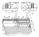
FIGS. 1A and 1B , which are simplified respective perspective and top view illustrations of an antenna constructed and operative in accordance with a preferred embodiment of the present invention. - As seen in
FIGS. 1A and 1B , there is provided anantenna 100, including aninductive element 102 and acapacitive element 104. -
Inductive element 102 andcapacitive element 104 are each preferably physically realized in a manner such that their physical dimensions and effective electrical lengths comprise non-trivial portions of an operating wavelength ofantenna 100. By way of example,inductive element 102 andcapacitive element 104 may have respective effective electrical lengths equal to approximately a sixth and an eighth of an operating wavelength ofantenna 100. - The formation of
antenna 100 from inductive and capacitive elements of such non-trivial physical and electrical lengths is in direct contrast to the typical usage of small lumped-element type inductors and capacitors within antenna structures and impedance matching networks conventionally employed by wireless devices. The use of comparatively large physically and electrically sized reactive elements confers significant operational advantages toantenna 100, by allowinginductive element 102 to act as a spatially- and phase-distributed feed element ofcapacitive element 104, as will be explained in greater detail below. - In the embodiment illustrated in
FIGS. 1A and 1B ,inductive element 102 is shown as a three-dimensional cylindrical helix andcapacitive element 104 is shown as a parallel plate capacitor, preferably comprising aninner capacitor plate 106, anouter capacitor plate 108 and adielectric core 110. It is appreciated, however, that other embodiments ofinductive element 102 andcapacitive element 104 are also possible, including planar, flared, tapered, spiral, or meandered inductive structures and interlaced or coaxial capacitive structures. -
Inductive element 102 andcapacitive element 104 are preferably installed on a common surface of a printed circuit board (PCB) 112.Inductive element 102 andcapacitive element 104 are preferably formed as three-dimensional elements, mechanically positioned on and attached to the surface ofPCB 112 by way of a dielectric carrier. Alternatively,inductive element 102 andcapacitive element 104 may be printed on a dielectric substrate on the surface of PCB 1.12. PCB 112 preferably also includes aground plane region 114. -
Antenna 100 is preferably fed by afeed point 116, whichfeed point 116 is preferably contiguous with and connected to aconductive feed trunk 118.Antenna 100 is preferably compatible with a 50 Ohm RF input impedance, although it is appreciated thatantenna 100 may be configured so as to be compatible with other input impedances. - A first end of
inductive element 102 is preferably in galvanic contact both withfeed point 116 andinner capacitor plate 106, at aconnection point 120.Connection point 120 is preferably located onconductive feed trunk 118, as seen most clearly at cross-section A-A inFIG. 1A . A second end ofinductive element 102 is preferably in galvanic contact withouter capacitor plate 108 at aconnection point 122, as seen most clearly at cross-section B-B inFIG. 1A . - Contact between the second end of
inductive element 102 andinner capacitor plate 106 is preferably avoided by means of a through-hole 124 located betweencapacitor plates hole 124inductive element 102 passes. - In operation of
antenna 100, inner andouter capacitor plates feed point 116 viaconnection points Connection points inductive element 102, receive or radiate radio-frequency (RF) signals that are mutually out of phase. Preferably, the phase difference between RF signals atconnection points points - It will thus be appreciated that
inductive element 102, due to its size and the arrangement of itsconnection points capacitive element 104. - It will further be appreciated that the above described arrangement of
inductive element 102,capacitive element 104 andfeed point 116 is somewhat analogous to a distributed parallel inductor-capacitor (LC) circuit driven by an alternating current source, wherein the reactances of the inductive andcapacitive elements antenna 100, combine to create a distributed resonance response, markedly different from the typical resonance response associated with small lumped element inductors and capacitors. - In operation, the distributed resonance response arising from the net reactances of
inductive element 102 andcapacitive element 104 supplements the intrinsic monopole resonance responses of inner andouter capacitor plates antenna 100, thereby improving the radiation efficiency and widening the bandwidth ofantenna 100. - Furthermore, the galvanic connection between the inductive and
capacitive elements feed point 116 creates a low-impedance path for RF signals of any frequency betweenantenna 100 and a transceiver to which it may be connected. This distinguishesantenna 100 over conventional enhanced-bandwidth antennas in which higher RF impedances between non-galvanically connected antenna elements tend to minimize the portion of low frequency signal energy conducted to the transceiver.Antenna 100 is therefore particularly advantageous for low frequency wireless applications. - As seen in
FIGS. 1A and 1B ,inner capacitor plate 106 andouter capacitor plate 108 preferably have substantially similar lengths and are largely overlapping. This structure enhances the radiation efficiency and widens the operational bandwidth ofantenna 100 over a single, relatively wide, band of interest. For example, the antenna embodiment ofFIGS. 1A and 1B may be designed to improve the radiation efficiency of the entire range of WiMax operating bands, from 2.3-3.7 GHz. - The realizable bandwidth and radiation efficiency of
antenna 100 may be modified by the adjustment of various geometric parameters associated withinductive element 102 andcapacitive element 104, whereby their reactances and hence distributed resonance may be modulated. Methods for modulating the reactances of inductors and capacitors are well known in the art and include, by way of example, changing the number or spacing of turns ofinductive element 102 and modifying the dimensions or separation of inner andouter capacitor plates - A tunable variant of
antenna 100 may be created by the incorporation of tuning components, such as RF switches and variable capacitors, into the antenna structure illustrated inFIGS. 1A and 1B . Such tuning components may be added in the form of discrete surface mount technology (SMT) components. In cases where the tuning components may potentially generate intermodulation products beyond the permissible limits of a device to whichantenna 100 is connected, the tuning components may be installed in a topology which minimizes the net intermodulation products, thereby satisfying the design requirements of the host device. - In addition to
inductive element 102 andcapacitive element 104, other radiating and/or phasing elements may be included inantenna 100 in order to satisfy the frequency requirements of a host device.Antenna 100 may thus be adapted for operation in a wide range of devices and over a wide range of operating frequencies, including FM, DVB-H, RFID, WiFi and WiMax. - The operation of
antenna 100 may be further enhanced by the inclusion of a conventional discrete passive component matching circuit betweenfeed point 116 and the terminal end of a transmission line connected to a transceiver (not shown). - Reference is now made to
FIGS. 2A and 2B which are simplified respective perspective and top view illustrations of an antenna constructed and operative in accordance with another preferred embodiment of the present invention. - As seen in
FIGS. 2A and 2B there is provided anantenna 200, including aninductive element 202 and acapacitive element 204.Capacitive element 204 preferably comprises aninner capacitor plate 206 and anouter capacitor plate 208, mutually separated by adielectric core 210.Inductive element 202 andcapacitive element 204 are preferably installed on a dielectric surface of aPCB 212, whichPCB 212 preferably also includes aground plane region 214.Antenna 200 is preferably fed by afeed point 216, which feedpoint 216 is preferably contiguous with and connected to aconductive feed trunk 218. A first end ofinductive element 202 is preferably galvanically connected both to feedpoint 216 andinner capacitor plate 206 at aconnection point 220, whichconnection point 220 is preferably located onconductive feed trunk 218. A second end ofinductive element 202 is preferably connected toouter capacitor plate 208 at aconnection point 222. The second end ofinductive element 202 preferably avoids contact withinner capacitor plate 206 by way of a through-hole 224 through which it passes. -
Antenna 200 may resembleantenna 100 in every relevant respect with the exception of the relative lengths ofinner capacitor plate 206 andouter capacitor plate 208. Whereas inantenna 100inner capacitor plate 106 andouter capacitor plate 108 have substantially similar lengths and largely overlap, inantenna 200inner capacitor plate 206, although partially overlapping withouter capacitor plate 208, is significantly shorter thanouter capacitor plate 208. The disparity in length of the twocapacitor plates antenna 100.Antenna 200 thus may be advantageous, for example, in providing a dual resonance antenna response for the GSM 850/900/1800/1900 operating bands. - It is appreciated that although in the embodiment of
antenna 200 illustrated inFIGS. 2A and 2B inner capacitor plate 206 is shown as shorter thanouter capacitor plate 208, a converse design in whichouter capacitor plate 208 is shorter thaninner capacitor plate 206 is also possible. - Other features and advantages of
antenna 200 are substantially as described above in reference toantenna 100 ofFIGS. 1A and 1B . - It will be appreciated by persons skilled in the art that the present invention is not limited by what has been particularly claimed hereinbelow. Rather the scope of the present invention includes various combinations and subcombinations of the features described hereinabove as well as modifications and variations thereof as would occur to persons skilled in the art upon reading the foregoing description with reference to the drawings and which are not in the prior art.
Claims (19)
1. An antenna comprising:
a capacitive element; and
an inductive element having first and second ends,
said first end of said inductive element being galvanically connected both to a feed point and to said capacitive element at a first connection point,
said second end of said inductive element being galvanically connected to said capacitive element at a second connection point, said second connection point being spatially displaced from said first connection point,
wherein electrical signals at said first and second connection points are mutually out of phase.
2. An antenna according to claim 1 , wherein a phase difference between said electrical signals at said first and second connection points is significantly greater than a phase difference associated with a straight line displacement between said first and second connection points.
3. An antenna according to claim 1 , wherein said inductive element comprises a spatially- and phase-distributed feed element.
4. An antenna according to claim 1 , wherein said inductive element has an electrical length comprising a non-trivial portion of an operating wavelength of said antenna.
5. An antenna according to claim 4 , wherein said capacitive element has an electrical length comprising a non-trivial portion of said operating wavelength of said antenna.
6. An antenna according to claim 1 , wherein said antenna is formed on a dielectric surface of a printed circuit board (PCB).
7. An antenna according to claim 6 , wherein said PCB includes a ground plane region.
8. An antenna according to claim 6 , wherein said inductive element and said capacitive element comprise printed elements on said surface of said PCB.
9. An antenna according to claim 6 , wherein said inductive element and said capacitive element comprise three-dimensional elements.
10. An antenna according to claim 9 , wherein said inductive element comprises a cylindrical coil.
11. An antenna according to claim 10 , wherein said capacitive element comprises two parallel conductive plates separated by a dielectric material
12. An antenna according to claim 11 , wherein said parallel conductive plates have substantially similar lengths, whereby a bandwidth of a single band of operation of said antenna is widened.
13. An antenna according to claim 12 , wherein said band of operation comprises 2.3-3.7 GHz.
14. An antenna according to claim 11 , wherein said parallel conductive plates have substantially dissimilar lengths, whereby bandwidths of multiple bands of operation of said antenna are widened.
15. An antenna according to claim 14 , wherein said multiple bands of operation comprise GSM 900 and GSM 1800.
16. An antenna according to claim 1 , also comprising tuning components.
17. An antenna according to claim 16 , wherein said tuning components comprise at least one of a variable capacitor and a radio-frequency switch.
18. An antenna according to claim 16 , wherein said tuning components are mounted on said antenna using surface mount technology methods.
19. An antenna according to claim 1 , also comprising additional radiating elements.
Priority Applications (1)
| Application Number | Priority Date | Filing Date | Title |
|---|---|---|---|
| US13/505,322 US20120249387A1 (en) | 2009-11-02 | 2010-11-02 | Distributed reactance antenna |
Applications Claiming Priority (3)
| Application Number | Priority Date | Filing Date | Title |
|---|---|---|---|
| US28036609P | 2009-11-02 | 2009-11-02 | |
| PCT/IL2010/000911 WO2011051954A1 (en) | 2009-11-02 | 2010-11-02 | Distributed reactance antenna |
| US13/505,322 US20120249387A1 (en) | 2009-11-02 | 2010-11-02 | Distributed reactance antenna |
Publications (1)
| Publication Number | Publication Date |
|---|---|
| US20120249387A1 true US20120249387A1 (en) | 2012-10-04 |
Family
ID=43921438
Family Applications (1)
| Application Number | Title | Priority Date | Filing Date |
|---|---|---|---|
| US13/505,322 Abandoned US20120249387A1 (en) | 2009-11-02 | 2010-11-02 | Distributed reactance antenna |
Country Status (5)
| Country | Link |
|---|---|
| US (1) | US20120249387A1 (en) |
| KR (1) | KR20120091264A (en) |
| CN (1) | CN102648552A (en) |
| DE (1) | DE112010004247T5 (en) |
| WO (1) | WO2011051954A1 (en) |
Families Citing this family (1)
| Publication number | Priority date | Publication date | Assignee | Title |
|---|---|---|---|---|
| US10027025B2 (en) * | 2012-08-29 | 2018-07-17 | Htc Corporation | Mobile device and antenna structure therein |
Citations (4)
| Publication number | Priority date | Publication date | Assignee | Title |
|---|---|---|---|---|
| US4038662A (en) * | 1975-10-07 | 1977-07-26 | Ball Brothers Research Corporation | Dielectric sheet mounted dipole antenna with reactive loading |
| US4571595A (en) * | 1983-12-05 | 1986-02-18 | Motorola, Inc. | Dual band transceiver antenna |
| US6888504B2 (en) * | 2002-02-01 | 2005-05-03 | Ipr Licensing, Inc. | Aperiodic array antenna |
| US7423598B2 (en) * | 2006-12-06 | 2008-09-09 | Motorola, Inc. | Communication device with a wideband antenna |
Family Cites Families (8)
| Publication number | Priority date | Publication date | Assignee | Title |
|---|---|---|---|---|
| US4980695A (en) * | 1989-11-22 | 1990-12-25 | Blaese Herbert R | Side antenna |
| KR19990010968A (en) * | 1997-07-19 | 1999-02-18 | 윤종용 | Dual band antenna |
| US6097349A (en) | 1997-11-18 | 2000-08-01 | Ericsson Inc. | Compact antenna feed circuits |
| US7154440B2 (en) * | 2001-04-11 | 2006-12-26 | Kyocera Wireless Corp. | Phase array antenna using a constant-gain phase shifter |
| US6885345B2 (en) * | 2002-11-14 | 2005-04-26 | The Penn State Research Foundation | Actively reconfigurable pixelized antenna systems |
| GB0317305D0 (en) * | 2003-07-24 | 2003-08-27 | Koninkl Philips Electronics Nv | Improvements in or relating to planar antennas |
| WO2006080141A1 (en) | 2005-01-27 | 2006-08-03 | Murata Manufacturing Co., Ltd. | Antenna and wireless communication device |
| FR2907969B1 (en) * | 2006-10-27 | 2009-04-24 | Groupe Ecoles Telecomm | MONO OR MULTI FREQUENCY ANTENNA |
-
2010
- 2010-11-02 WO PCT/IL2010/000911 patent/WO2011051954A1/en not_active Ceased
- 2010-11-02 CN CN201080049228XA patent/CN102648552A/en active Pending
- 2010-11-02 US US13/505,322 patent/US20120249387A1/en not_active Abandoned
- 2010-11-02 KR KR1020127014007A patent/KR20120091264A/en not_active Withdrawn
- 2010-11-02 DE DE112010004247T patent/DE112010004247T5/en not_active Withdrawn
Patent Citations (4)
| Publication number | Priority date | Publication date | Assignee | Title |
|---|---|---|---|---|
| US4038662A (en) * | 1975-10-07 | 1977-07-26 | Ball Brothers Research Corporation | Dielectric sheet mounted dipole antenna with reactive loading |
| US4571595A (en) * | 1983-12-05 | 1986-02-18 | Motorola, Inc. | Dual band transceiver antenna |
| US6888504B2 (en) * | 2002-02-01 | 2005-05-03 | Ipr Licensing, Inc. | Aperiodic array antenna |
| US7423598B2 (en) * | 2006-12-06 | 2008-09-09 | Motorola, Inc. | Communication device with a wideband antenna |
Also Published As
| Publication number | Publication date |
|---|---|
| WO2011051954A1 (en) | 2011-05-05 |
| DE112010004247T5 (en) | 2013-01-24 |
| KR20120091264A (en) | 2012-08-17 |
| CN102648552A (en) | 2012-08-22 |
Similar Documents
| Publication | Publication Date | Title |
|---|---|---|
| CA2813829C (en) | A loop antenna for mobile handset and other applications | |
| JP5983769B2 (en) | Multiband antenna | |
| US9385433B2 (en) | Multiband hybrid antenna | |
| EP1791213A1 (en) | Multiband antenna component | |
| CA3084990A1 (en) | Dipole antenna | |
| CN108352621B (en) | Antenna device | |
| WO2014059382A1 (en) | Multiband antenna | |
| US20110285596A1 (en) | Inductively coupled band selectable and tunable antenna | |
| EP2437348B1 (en) | Branched UWB antenna | |
| US10992045B2 (en) | Multi-band planar antenna | |
| US7542002B1 (en) | Wideband monopole antenna | |
| WO2011154955A2 (en) | Single-branch multiband antenna | |
| US20120249387A1 (en) | Distributed reactance antenna | |
| EP2661788A2 (en) | Compact broadband antenna | |
| JPH09232854A (en) | Small planar antenna device for mobile radio | |
| KR101708570B1 (en) | Triple Band Ground Radiation Antenna | |
| KR101480592B1 (en) | Antenna apparatus and feeding structure thereof | |
| KR20140143969A (en) | Antenna apparatus and feeding structure thereof | |
| KR101470086B1 (en) | Antenna apparatus | |
| CA3101992A1 (en) | Multi-band planar antenna | |
| KR20140121622A (en) | Antenna apparatus and feeding structure thereof | |
| HK1181188A (en) | Single-branch multiband antenna | |
| JP2009065565A (en) | antenna | |
| KR20100046506A (en) | Minimized antenna apparatus | |
| CN112635982A (en) | Short-circuit coplanar waveguide-fed dual-polarized broadband antenna |
Legal Events
| Date | Code | Title | Description |
|---|---|---|---|
| AS | Assignment |
Owner name: GALTRONICS CORPORATION LTD., ISRAEL Free format text: ASSIGNMENT OF ASSIGNORS INTEREST;ASSIGNOR:KRUPA, STEVE;REEL/FRAME:028362/0464 Effective date: 20120507 |
|
| STCB | Information on status: application discontinuation |
Free format text: ABANDONED -- FAILURE TO RESPOND TO AN OFFICE ACTION |