US20120249283A1 - Flex-rigid wiring board and method for manufacturing the same - Google Patents
Flex-rigid wiring board and method for manufacturing the same Download PDFInfo
- Publication number
- US20120249283A1 US20120249283A1 US13/145,455 US201013145455A US2012249283A1 US 20120249283 A1 US20120249283 A1 US 20120249283A1 US 201013145455 A US201013145455 A US 201013145455A US 2012249283 A1 US2012249283 A1 US 2012249283A1
- Authority
- US
- United States
- Prior art keywords
- soluble conductor
- protection element
- flux
- insulation cover
- conductor
- Prior art date
- Legal status (The legal status is an assumption and is not a legal conclusion. Google has not performed a legal analysis and makes no representation as to the accuracy of the status listed.)
- Granted
Links
Images


Classifications
-
- H—ELECTRICITY
- H01—ELECTRIC ELEMENTS
- H01H—ELECTRIC SWITCHES; RELAYS; SELECTORS; EMERGENCY PROTECTIVE DEVICES
- H01H37/00—Thermally-actuated switches
- H01H37/74—Switches in which only the opening movement or only the closing movement of a contact is effected by heating or cooling
- H01H37/76—Contact member actuated by melting of fusible material, actuated due to burning of combustible material or due to explosion of explosive material
- H01H37/761—Contact member actuated by melting of fusible material, actuated due to burning of combustible material or due to explosion of explosive material with a fusible element forming part of the switched circuit
-
- H—ELECTRICITY
- H01—ELECTRIC ELEMENTS
- H01H—ELECTRIC SWITCHES; RELAYS; SELECTORS; EMERGENCY PROTECTIVE DEVICES
- H01H1/00—Contacts
- H01H1/58—Electric connections to or between contacts; Terminals
- H01H1/5805—Connections to printed circuits
-
- H—ELECTRICITY
- H01—ELECTRIC ELEMENTS
- H01H—ELECTRIC SWITCHES; RELAYS; SELECTORS; EMERGENCY PROTECTIVE DEVICES
- H01H37/00—Thermally-actuated switches
- H01H37/74—Switches in which only the opening movement or only the closing movement of a contact is effected by heating or cooling
- H01H37/76—Contact member actuated by melting of fusible material, actuated due to burning of combustible material or due to explosion of explosive material
- H01H2037/768—Contact member actuated by melting of fusible material, actuated due to burning of combustible material or due to explosion of explosive material characterised by the composition of the fusible material
-
- Y—GENERAL TAGGING OF NEW TECHNOLOGICAL DEVELOPMENTS; GENERAL TAGGING OF CROSS-SECTIONAL TECHNOLOGIES SPANNING OVER SEVERAL SECTIONS OF THE IPC; TECHNICAL SUBJECTS COVERED BY FORMER USPC CROSS-REFERENCE ART COLLECTIONS [XRACs] AND DIGESTS
- Y10—TECHNICAL SUBJECTS COVERED BY FORMER USPC
- Y10T—TECHNICAL SUBJECTS COVERED BY FORMER US CLASSIFICATION
- Y10T29/00—Metal working
- Y10T29/49—Method of mechanical manufacture
- Y10T29/49002—Electrical device making
- Y10T29/49107—Fuse making
Definitions
- the flux functions as an activator for preventing oxidization of a soluble conductor and for causing a blowout exerted by an overcurrent or an overvoltage, and a retention state of the flux influences an operation speed.
- a halogen-free flux which does not contain a halogen component, such as boron (Br)
- the state of the flux greatly influences a blowout speed or stability of the soluble conductor.
- the flux 9 on the soluble conductor 3 is not stably retained at a central part of the space 8 , and may be unevenly distributed at the left or right.
- a fused metal of the soluble conductor 3 is likely to flow in a location in which the flux 9 could be retained; and the soluble conductor 3 is hardly fused at a portion at which the flux 9 is insufficient, and there is a problem that time taken for reliable blowout is extended.
- the present invention has been made in view of the above-described background art, and it is an object of the present invention to provide a protection element which is capable of stably retaining a flux on a soluble conductor at a predetermined position, enabling a speedy and precise blowout of the soluble conductor in the event of an abnormality.
- the present invention is directed to a protection element including: a soluble conductor which is disposed on an insulation baseboard and is connected to a power supply path of a device targeted to be protected, to cause a blowout due to a predetermined abnormal electric power; an insulation cover which is mounted on the baseboard with the soluble conductor being covered via a predetermined space; and a flux which is applied to a surface of the soluble conductor and is positioned in the space, the protection element being adapted for, in case that the abnormal electric power is supplied to the device targeted to be protected, allowing the soluble conductor to cause a blowout and then to shut off a current path of the conductor, the protection element comprising a stepped portion which is formed on an interior face of the insulation cover in opposite to the soluble conductor, for retaining the flux at a predetermined position in the space in contact with the flux, wherein a hole portion retaining the flux is formed at the soluble conductor.
- the hole portion of the soluble conductor is a through hole formed at the center part of the soluble conductor.
- the stepped portion is made of a protrusive stripe portion which is formed on the interior face of the insulation cover and which is provided in face-to-face opposite to the hole portion of the soluble conductor.
- a protrusive portion may be formed along a circumferential edge part.
- a relatively small hole portion other than the center part of the soluble conductor may be formed at the soluble conductor, and a number of small hole portions may be formed at the soluble conductor. Further, an opening portion which is a through hole may be formed inside of the stepped portion of the insulation cover.
- a flux By forming a small hole portion other than a flux retaining portion of a soluble conductor, a flux can be reliably retained at a peripheral portion of the soluble conductor, and a blowout volume is also reduced, thus enabling a reliable blowout for a short period of time in the event of an abnormality.
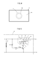
- FIG. 1 It is a plan view of a state in which an insulation cover is removed from a protection element according to a first embodiment of the present invention.
- FIG. 2 It is a sectional view taken along the line A-A of FIG. 1 , of a state in which the insulation cover is mounted on the protection element of FIG. 1 .
- FIG. 3 It is a plan view (a) before mounting a soluble conductor on the protection element according to the first embodiment of the present invention and it is a plan view (b) of the soluble conductor.
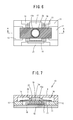
- FIG. 7 It is a sectional view taken along the line A-A of FIG. 6 , of a state in which the insulation cover is mounted on the protection element of FIG. 6 .
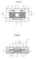
- FIG. 10 It is a plan view of a state in which an insulation cover is removed from a protection element according to a fourth embodiment of the present invention.
- FIG. 14 It is a longitudinal cross section showing an appearance of a flux of the conventional protection element.
- a protection element 10 of the embodiment has a pair of electrodes 12 which is formed on both ends of a top face of an insulation baseboard 11 , and the other pair of electrodes 21 is provided at opposite edge parts which are orthogonal to the pair of electrodes 12 .
- a heating element 15 made of a resistor is connected between the electrodes 21 .
- a conductor layer 17 which is connected to one electrode 21 is laminated via an insulation layer 16 .
- a center part of a soluble conductor 13 which is a fuse made of a low-melting metal connected to the pair of electrodes 12 is connected to the conductor layer 17 .
- an insulation cover 14 as an insulation member is provided in face-to-face opposite to the soluble conductor 13 .
- any kind of material may be employed as long as it has an insulation property, and for example, an insulation board employed for a printed wiring board, such as a ceramic board or a glass epoxy board, is preferable.
- an insulation board employed for a printed wiring board such as a ceramic board or a glass epoxy board
- a glass board, a resin board, or an insulation processing metal board or the like can be employed for appropriate usage, whereas a ceramic board with its superior heat resistance and its good thermal conductivity is further preferable.
- the electrodes 12 , 21 and the conductor layer 17 there can be used a metal foil such as copper or a conductor material whose surface is plated with Ag-Pt, Au, or the like.
- a hole portion 13 a made of an annular through hole formed at a center part thereof is formed.
- the hole portion 13 a is formed in a circular shape, and is face-to-face opposed to be positioned concentrically with a protrusive stripe portion 20 of an insulation cover 14 to be described later.
- a low-melting metal foil of the soluble conductor 13 may be employed as long as it is fused at a predetermined electric power, and a variety of low-melting metals which are publicly known can be used as materials for fuse.
- a BiSnPb alloy for example, a BiSnPb alloy, a BiPbSn alloy, a BiPb alloy, a BiSn alloy, a SnPb alloy, a SnAg alloy, a PbIn alloy, a ZnAl alloy, an InSn alloy, a PbAgSn alloy or the like can be employed.
- a flux 19 is provided in order to prevent oxidization of the surface.
- a halogen-free flux which does not have a halogen element such as boron is preferable.
- the flux 19 is filled in the hole portion 13 a of the soluble conductor 13 ; further stays at the periphery thereof, and is retained on the soluble conductor 13 by means of surface tension. Further, the flux 19 rises and is housed in the space 18 of the insulation cover 14 , by means of surface tension, and as shown in FIG.
- a protection operation of the protection element 10 of the embodiment will be described.
- a secondary battery device such as a lithium ion battery on which the overcurrent or overvoltage protection circuit 26 of the embodiment has been mounted
- an abnormal voltage is applied to the output terminals A 1 and A 2 at the time of power charging thereof
- an inversed voltage which is equal to or greater than a breakdown voltage is applied to the Zener diode ZD at a predetermined voltage which is set to be abnormal, and then, the Zener diode ZD is made conductive.
- a small hole portion 13 b which is a relatively small hole portion is formed at another position as well, in addition to the protrusive portion 20 having the stepped portion 20 a and the hole portion 13 a at the center part of the soluble conductor 13 , of the interior face 14 a of the insulation cover 14 .
- a flux 19 can be stably retained at a center part by means of the hole portion 13 a ; the flux 19 is retained at a small hole portion 13 b even at a position other than the center part of the soluble conductor 13 ; and blowout characteristics of the soluble conductor 13 are made more stable.
- the protrusive portion 22 of the second embodiment may be formed on the soluble conductor 13 of the embodiment. In this manner, the position of the flux 19 is further stabilized and then its blowout characteristics are improved.
Landscapes
- Chemical & Material Sciences (AREA)
- Engineering & Computer Science (AREA)
- Combustion & Propulsion (AREA)
- Fuses (AREA)
Abstract
Description
- The present invention relates to a protection element for, in case that an overcurrent or an overvoltage is applied to an electronic device or the like, allowing a soluble conductor to cause a blowout exerted by a heat of such an overcurrent or overvoltage and then to shut off a current.
- Conventionally, a protection element which is mounted on a secondary battery device or the like is employed as the one that has a function of preventing an overvoltage as well as an overcurrent. This protection element is formed so that: a heating element and a soluble conductor made of a low-melting metal member are laminated on a board; the soluble conductor is blown out due to an overcurrent; and in case that an overvoltage is generated as well, power is supplied to the heating element in the protection element and then the soluble conductor is blown out due to a heat of the heating element. Blowout of the soluble conductor takes place due to goodness of wettability relative to a surface of a connected electrode at the time of blowout of the soluble conductor that is a low-melting metal. The low-melting metal that has been blown out is attracted onto an electrode, and as a result, the soluble conductor is broken and then a current is shut off.
- On the other hand, with downsizing of an electronic device, such as a portable device, in recent years, there has been a need for downsizing or thinning a protection element of this type; and there has been a further demand for operational stability and fastness. As a means therefor, there is provided the one in which a soluble conductor of a low-melting metal member is disposed on an insulation board; the thus disposed soluble conductor is sealed with an insulation cover; and a flux is coated onto the soluble conductor. This flux is adapted to prevent oxidization of a surface of the soluble conductor, and is provided so that the soluble conductor blows out speedily and stably at the time of heating the soluble conductor.
- Such a protection element has a structure shown in
FIG. 13 . In this protection element, a pair ofelectrodes 2 is provided on abaseboard 1, and a pair of electrodes, although not shown, is provided at an opposite edge part which is orthogonal to theelectrodes 2 as well. Aheating element 5 made of a resistor is provided between electrodes, although not shown, and a conductor layer 7 which is connected to one of the pair of electrodes, although not shown, via aninsulation layer 6, is provided. At this protection element, a soluble conductor 3 made of a low-melting metal foil is provided between the pair ofelectrodes 2 that is formed on both ends of thebaseboard 1. A center part of the soluble conductor 3 is provided on the conductor layer 7. Further, aninsulation cover 4 is provided in face-to-face opposite to the soluble conductor 3 that is provided on thebaseboard 1. Theinsulation cover 4 which is mounted on thebaseboard 1 is put with apredetermined space 8 being formed relative to the soluble conductor 3. Aflux 9 is coated onto the soluble conductor 3, and theflux 9 is housed in thespace 8 which is provided in theinsulation cover 4. - In addition, as disclosed in
Patent Document 1, as a protection element for shortening a circuit shutoff time due to coagulation at the time of blowout of a low-melting metal member and then reducing a difference in operation time, there is provided the one in which a low-melting metal member having two stripes or a low-melting metal member forming a slit in an intra-electrode direction is provided between a pair of electrodes supplying a current to the low-melting metal member. This protection element is capable of segmenting the low-melting metal member between the electrodes in an independent state, increasing the number of blowout start points in low-melting metal member, and then, reducing and stabilizing an operation time. - [Patent Document 1] Japanese Patent Application Laid-open No. 2004-214032
- In a protection element in which a flux is provided at a soluble conductor of a low-melting metal, the flux functions as an activator for preventing oxidization of a soluble conductor and for causing a blowout exerted by an overcurrent or an overvoltage, and a retention state of the flux influences an operation speed. In particular, in a process of manufacturing an electronic device or in a process of waste management, in order to mitigate an environmental burden, in a case where a halogen-free flux which does not contain a halogen component, such as boron (Br), is used, since the flux of this type is low in degree of activity, the state of the flux greatly influences a blowout speed or stability of the soluble conductor.
- That is, as shown in
FIG. 14 , in theinsulation cover 4, theflux 9 on the soluble conductor 3 is not stably retained at a central part of thespace 8, and may be unevenly distributed at the left or right. In such a case, there emerges a circumstance that: a fused metal of the soluble conductor 3 is likely to flow in a location in which theflux 9 could be retained; and the soluble conductor 3 is hardly fused at a portion at which theflux 9 is insufficient, and there is a problem that time taken for reliable blowout is extended. - Further, as in the invention set forth in
Patent Document 1, in a case where a low-melting metal member having two or more stripes or a low-melting metal member forming a slit has been formed as well, there arises a problem exerted by a flux having its low degree of activity such as the abovementioned halogen-free flux, and further forming of a slit or the like requires a special molding die on the manufacture of a protection element, resulting in higher manufacturing costs. - The present invention has been made in view of the above-described background art, and it is an object of the present invention to provide a protection element which is capable of stably retaining a flux on a soluble conductor at a predetermined position, enabling a speedy and precise blowout of the soluble conductor in the event of an abnormality.
- The present invention is directed to a protection element including: a soluble conductor which is disposed on an insulation baseboard and is connected to a power supply path of a device targeted to be protected, to cause a blowout due to a predetermined abnormal electric power; an insulation cover which is mounted on the baseboard with the soluble conductor being covered via a predetermined space; and a flux which is applied to a surface of the soluble conductor and is positioned in the space, the protection element being adapted for, in case that the abnormal electric power is supplied to the device targeted to be protected, allowing the soluble conductor to cause a blowout and then to shut off a current path of the conductor, the protection element comprising a stepped portion which is formed on an interior face of the insulation cover in opposite to the soluble conductor, for retaining the flux at a predetermined position in the space in contact with the flux, wherein a hole portion retaining the flux is formed at the soluble conductor.
- The hole portion of the soluble conductor is a through hole formed at the center part of the soluble conductor. The stepped portion is made of a protrusive stripe portion which is formed on the interior face of the insulation cover and which is provided in face-to-face opposite to the hole portion of the soluble conductor. In addition, on a peripheral surface of the hole portion at the center part of the soluble conductor, a protrusive portion may be formed along a circumferential edge part.
- Further, a relatively small hole portion other than the center part of the soluble conductor may be formed at the soluble conductor, and a number of small hole portions may be formed at the soluble conductor. Further, an opening portion which is a through hole may be formed inside of the stepped portion of the insulation cover.
- According to a protection element of the present invention, a stepped portion for retaining a flux is provided inside of an insulation cover, and a hole portion is provided at a soluble conductor, thus enabling the flux to be stably retained at a predetermined position of the soluble conductor. In this manner, in particular, in a case where a flux with its low degree of activity (such as a halogen-free flux) is used as well, it is possible to prevent uneven distribution of the degree of activity due to bias of a flux retention state after applying the flux. Further, in blowout operation of a soluble conductor, in particular, in heating operation characteristics of low electric power, an operational distortion can be remarkably reduced. Moreover, a protection element with its small environmental burden can be provided by employing a halogen-free flux. A fusion volume can be reduced while a conventional foil size of a soluble conductor is maintained, enabling an easier blowout.
- By forming a small hole portion other than a flux retaining portion of a soluble conductor, a flux can be reliably retained at a peripheral portion of the soluble conductor, and a blowout volume is also reduced, thus enabling a reliable blowout for a short period of time in the event of an abnormality.
- By forming a protrusive portion around a hole portion of a soluble conductor, a flux can be retained further reliably, contributing to stabilization of blowout characteristics.
- By providing an opening portion at an insulation cover, it becomes possible to visually check the inside of a flux for appearance.
- [
FIG. 1 ] It is a plan view of a state in which an insulation cover is removed from a protection element according to a first embodiment of the present invention. - [
FIG. 2 ] It is a sectional view taken along the line A-A ofFIG. 1 , of a state in which the insulation cover is mounted on the protection element ofFIG. 1 . - [
FIG. 3 ] It is a plan view (a) before mounting a soluble conductor on the protection element according to the first embodiment of the present invention and it is a plan view (b) of the soluble conductor. - [
FIG. 4 ] It is a plan view of an insulation cover of the protection element according to the first embodiment of the present invention. - [
FIG. 5 ] It is a circuit diagram of a secondary battery device providing the protection element according to the first embodiment of the present invention. - [
FIG. 6 ] It is a plan view of a state in which an insulation cover is removed from a protection element according to a second embodiment of the present invention. - [
FIG. 7 ] It is a sectional view taken along the line A-A ofFIG. 6 , of a state in which the insulation cover is mounted on the protection element ofFIG. 6 . - [
FIG. 8 ] It is a plan view of a state in which an insulation cover is removed from a protection element according to a third embodiment of the present invention. - [
FIG. 9 ] It is a sectional view taken along the line A-A ofFIG. 8 , of a state in which the insulation cover is mounted on the protection element ofFIG. 8 . - [
FIG. 10 ] It is a plan view of a state in which an insulation cover is removed from a protection element according to a fourth embodiment of the present invention. - [
FIG. 11 ] It is a sectional view taken along the line A-A ofFIG. 10 , of a state in which the insulation cover is mounted on the protection element ofFIG. 10 . - [
FIG. 12 ] It is a longitudinal cross section of a protection element according to a fifth embodiment of the present invention. - [
FIG. 13 ] It is a longitudinal cross section of a conventional protection element. - [
FIG. 14 ] It is a longitudinal cross section showing an appearance of a flux of the conventional protection element. - Hereinafter, a first embodiment of a protection element of the present invention will be described with reference to
FIGS. 1 to 5 . Aprotection element 10 of the embodiment has a pair ofelectrodes 12 which is formed on both ends of a top face of aninsulation baseboard 11, and the other pair ofelectrodes 21 is provided at opposite edge parts which are orthogonal to the pair ofelectrodes 12. Aheating element 15 made of a resistor is connected between theelectrodes 21. At theheating element 15, aconductor layer 17 which is connected to oneelectrode 21 is laminated via aninsulation layer 16. A center part of asoluble conductor 13 which is a fuse made of a low-melting metal connected to the pair ofelectrodes 12 is connected to theconductor layer 17. In addition, on thebaseboard 11, aninsulation cover 14 as an insulation member is provided in face-to-face opposite to thesoluble conductor 13. - As a material for the
baseboard 11, any kind of material may be employed as long as it has an insulation property, and for example, an insulation board employed for a printed wiring board, such as a ceramic board or a glass epoxy board, is preferable. In addition, a glass board, a resin board, or an insulation processing metal board or the like can be employed for appropriate usage, whereas a ceramic board with its superior heat resistance and its good thermal conductivity is further preferable. - As the
electrodes conductor layer 17, there can be used a metal foil such as copper or a conductor material whose surface is plated with Ag-Pt, Au, or the like. In addition, there may be employed a conductor layer or an electrode obtained by coating and firing an electrically conductive paste, such as an Ag paste, or alternatively, a metal thin-film structure obtained by evaporation or the like. - At the
soluble conductor 13, ahole portion 13 a made of an annular through hole formed at a center part thereof is formed. Thehole portion 13 a, as shown inFIG. 3 , is formed in a circular shape, and is face-to-face opposed to be positioned concentrically with aprotrusive stripe portion 20 of aninsulation cover 14 to be described later. A low-melting metal foil of thesoluble conductor 13 may be employed as long as it is fused at a predetermined electric power, and a variety of low-melting metals which are publicly known can be used as materials for fuse. For example, a BiSnPb alloy, a BiPbSn alloy, a BiPb alloy, a BiSn alloy, a SnPb alloy, a SnAg alloy, a PbIn alloy, a ZnAl alloy, an InSn alloy, a PbAgSn alloy or the like can be employed. - A resistor forming the
heating element 15 is obtained by coating and firing a resistance paste made of an electrically conductive material such as ruthenium oxide or carbon black and an inorganic binder such as glass or an organic binder such as thermal setting resin. In addition, this resistor may be formed by printing and firing a thin film of ruthenium oxide or carbon black or by means of plating, evaporation, or sputtering, or alternatively, may be formed by attaching or laminating a film of these resistor materials, for example. - The
insulation cover 14 that is mounted on thebaseboard 11 is formed in a box shape which opens at one side face, and is put on thebaseboard 11 with thepredetermined space 18 being formed relative to thesoluble conductor 13. As a material for theinsulation cover 14, there may be an insulation material having its heat resistance which is resistive to a heat at the time of blowout of thesoluble conductor 13, the insulation material having a mechanical strength which is identical to that of theprotection element 10. For example, a variety of materials such as board materials employed for printed wiring boards such as glass, ceramics, plastics, or glass epoxy resin can be applied. Further, an insulation layer such as an insulation resin may be formed on a face opposite to thebaseboard 11, by employing a metal plate. Preferably, a material with its mechanical strength and its high insulation property such as ceramics is preferable, since it contributes to thickness reduction of the entire protection element as well. - On an
interior face 14 a of theinsulation cover 14, a low cylindricalprotrusive stripe portion 20 which is provided with a concentrically circular steppedportion 20 a is formed at a position which is opposite to thehole portion 13 a at a center part of thesoluble conductor 13. Theprotrusive stripe portion 20 is formed integrally with theinsulation cover 14, and a projection position for thebaseboard 11 is positioned on theheating element 15. - On an entire surface of the
soluble conductor 13, aflux 19 is provided in order to prevent oxidization of the surface. As theflux 19, a halogen-free flux which does not have a halogen element such as boron is preferable. Theflux 19 is filled in thehole portion 13 a of thesoluble conductor 13; further stays at the periphery thereof, and is retained on thesoluble conductor 13 by means of surface tension. Further, theflux 19 rises and is housed in thespace 18 of theinsulation cover 14, by means of surface tension, and as shown inFIG. 2 , the housedflux 19 adheres to theprotrusive stripe portion 20 that is formed on theinterior face 14 a of theinsulation cover 14, and then, theresultant flux 19 is stably retained by means of the steppedportion 20 a due to its wettability. In this manner, theflux 19 is stably retained in thespace 18 of theinsulation cover 14 without being displaced from the center part of thesoluble conductor 13. - Here, a protrusion height from the insulation cover
interior face 14 a of theprotrusive stripe portion 20 is preferable to be a height to an extent such that a surface of theflux 19 coated onto thesoluble conductor 13 comes into contact and theflux 19 can be retained at the center part due to its wettability and surface tension. In addition, the protrusion height is limited to an extent such that, in respect of the fusedsoluble conductor 13 with a low-melting metal being fused due to abnormal electric power, a top part having spherically risen due to its surface tension just comes into contact with something. Preferably, the protrusion height is preferable to an extent such that the fusedsoluble conductor 13 does not come into contact with anything. - Next, as an example of employing the
protection element 10 of the embodiment in an electronic device, an overcurrent orovervoltage protection circuit 26 of a secondary battery device will be described with reference toFIG. 5 . In this overcurrent orovervoltage protection circuit 26, a pair ofelectrodes 12 of theprotection element 10 is connected in series between an output terminal Al and an input terminal B1, one terminal of the pair ofelectrodes 12 of theprotection element 10 is connected to the input terminal B1, and theother electrode 12 is connected to the output terminal A1. In addition, a neutral point of thesoluble conductor 13 is connected to one end of theheating element 15, and one terminal of theelectrode 21 is connected to the other terminal of theheating element 15. The other terminal of theheating element 15 is connected to a collector of a transistor Tr, and an emitter of the transistor Tr is connected between the other input terminal A2 and output terminal B2. Further, an anode of a Zener diode ZD is connected to a base of the transistor Tr via a resistor R, and a cathode of the Zener diode ZD is connected to the output terminal A1. The resistor R is set at a value such that when a predetermined value set to be abnormal is applied between the output terminals A1 and A2, a voltage beyond a breakdown voltage is applied to the Zener diode ZD. - Electrode terminals of the
secondary battery 23 which is a device targeted to be protected, such as a lithium ion battery, for example, are connected between the output terminals A1 and A2, and electrode terminals of a device such as a battery charger, although not shown, which is to be used to be connected to thesecondary battery 23, are connected to the input terminals B1 and B2. - Next, a protection operation of the
protection element 10 of the embodiment will be described. In a secondary battery device such as a lithium ion battery on which the overcurrent orovervoltage protection circuit 26 of the embodiment has been mounted, if an abnormal voltage is applied to the output terminals A1 and A2 at the time of power charging thereof, an inversed voltage which is equal to or greater than a breakdown voltage is applied to the Zener diode ZD at a predetermined voltage which is set to be abnormal, and then, the Zener diode ZD is made conductive. By making the Zener diode ZD conductive, a base current ib flows into a base of a transistor TR, whereby a transistor Tr is turned on, a collector current is flows into theheating element 15, and then, theheating element 15 generates a heat. This heat is transmitted to thesoluble conductor 13 of a low-melting metal on theheating element 15, thesoluble conductor 13 blows out, and then, an electric conduction between the input terminal B1 and the output terminal A1 is shut off, preventing an overvoltage from being applied to the output terminals A1 and A2. - At this time, the
flux 19 is retained at the center part of thesoluble conductor 13, and blows out speedily and reliably at a predetermined blowout position. In addition, in case that an abnormal current flows toward the output terminal A1 as well, thesoluble conductor 13 is set so as to generate a heat and then blow out due to the current. - According to the
protection element 10 of the embodiment, on theinterior face 14 a of theinsulation cover 14, a protrusive-shaped cylindricalprotrusive stripe portion 20 is provided to be face-to-face opposed to thesoluble conductor 13, and ahole portion 13 a is formed at the center part of thesoluble conductor 13 in opposite to theprotrusive stripe portion 20, thus enabling theflux 19 to be stably retained at a predetermined position at the center part of thesoluble conductor 13. In this manner, in particular, in a case where aflux 19 such as a halogen-free flux with its low degree of activity is used as well, it is possible to prevent uneven distribution of an action of the flux due to bias or distortion of a coating state of theflux 19, and a blowout of thesoluble conductor 13 is ensured. Further, a blowout volume is reduced by thehole portion 13 a of thesoluble conductor 13, so that blowout in the event of an abnormality is performed more reliably within a short period of time. - Next, a second embodiment of a protection element of the present invention will be described with reference to
FIGS. 6 and 7 . Herein, like constituent elements in the abovementioned embodiment are designated by like reference numerals, and a duplicate description is omitted. In aprotection element 10 of the embodiment, on aninterior face 14 a of aninsulation cover 14, a cylindricalprotrusive stripe portion 20 having a steppedportion 20 a is provided in opposite to asoluble conductor 13, and aprotrusive portion 22 is formed along a peripheral edge part of ahole portion 13 a of thesoluble conductor 13. - According to the
protection element 10 of the embodiment, it becomes possible to more stably retain theflux 19 at a predetermined position by means of theprotrusive portion 22, and blowout operation of thesoluble conductor 13 can be performed more stably. - Next, a third embodiment of a protection element of the present invention will be described with reference to
FIGS. 8 and 9 . Herein, like constituent elements in the above-described embodiments are designated by like reference numerals, and a duplicate description is omitted. According to the embodiment, asmall hole portion 13 b which is a relatively small hole portion is formed at another position as well, in addition to theprotrusive portion 20 having the steppedportion 20 a and thehole portion 13 a at the center part of thesoluble conductor 13, of theinterior face 14 a of theinsulation cover 14. - According to the
protection element 10 of the embodiment, aflux 19 can be stably retained at a center part by means of thehole portion 13 a; theflux 19 is retained at asmall hole portion 13 b even at a position other than the center part of thesoluble conductor 13; and blowout characteristics of thesoluble conductor 13 are made more stable. Theprotrusive portion 22 of the second embodiment may be formed on thesoluble conductor 13 of the embodiment. In this manner, the position of theflux 19 is further stabilized and then its blowout characteristics are improved. - Next, a fourth embodiment of a protection element of the present invention will be described with reference to
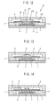
FIGS. 10 and 11 . Herein, like constituent elements in the above-described embodiment s are designated by like reference numerals, and a duplicate description is omitted. In the embodiment, while aprotrusive stripe portion 20 having a steppedportion 20 a, of aninterior face 14 a of aninsulation cover 14 is provided, asmall hole portion 13 b which is a relatively small hole portion is formed all over thesoluble conductor 13, in place of thehole portion 13 a at the center part of thesoluble conductor 13. - According to the
protection element 10 of the embodiment, aflux 19 can be stably retained at a center part by means of aprotrusive stripe portion 22 of theinsulation cover 14 and thesmall hole portion 13 b of thesoluble conductor 13, and aflux 19 is retained at a peripheral part of thesoluble conductor 13 as well, by means of thesmall hole portion 13 b other than the center part of thesoluble conductor 13, thereby stabilizing blowout characteristics. - Next, a fifth embodiment of a protection element of the present invention will be described with reference to
FIG. 12 . Herein, like constituent elements in the above-described embodiments are designated by like reference numerals, and a duplicate description is omitted. In aprotection element 13 of the embodiment, an openingportion 24 is provided at a center part at which aprotrusive stripe portion 20 of aninsulation cover 14 is positioned, together with a cylindrical-shapedprotrusive stripe portion 20 having a steppedportion 20 a, of aninterior face 14 a of theinsulation cover 14. - According to the
protection element 10 of the embodiment, in addition to an advantageous effect similar to that of the above-described embodiment, which is exerted by theprotrusive stripe portion 20 of the openingportion 24, a retention state of aflux 19 can be visually checked with naked eyes through the openingportion 24, and product check can be made more easily and reliably. The openingportion 24 may be sealed with a transparent glass or a resin. This makes it possible to prevent the entry of dust or the like though the openingportion 24. In addition, theprotrusive stripe portion 20 may not be formed by means of a stepped portion caused by the openingportion 24. - The protection element of the present invention is not limited to the above-described embodiments, and may be formed in the shapes of an insulation cover and a soluble conductor which are capable of retaining a flux at a predetermined position in a space provided in the insulation cover, irrespective of any retention mode thereof. In addition, any kind of material for the flux or insulation cover can be selected as long as it functions properly.
Claims (7)
Applications Claiming Priority (3)
| Application Number | Priority Date | Filing Date | Title |
|---|---|---|---|
| JP2009011197A JP5130232B2 (en) | 2009-01-21 | 2009-01-21 | Protective element |
| JP2009-011197 | 2009-01-21 | ||
| PCT/JP2010/050335 WO2010084818A1 (en) | 2009-01-21 | 2010-01-14 | Protection element |
Publications (2)
| Publication Number | Publication Date |
|---|---|
| US20120249283A1 true US20120249283A1 (en) | 2012-10-04 |
| US8803652B2 US8803652B2 (en) | 2014-08-12 |
Family
ID=42355872
Family Applications (1)
| Application Number | Title | Priority Date | Filing Date |
|---|---|---|---|
| US13/145,455 Active 2030-04-06 US8803652B2 (en) | 2009-01-21 | 2010-01-14 | Protection element |
Country Status (7)
| Country | Link |
|---|---|
| US (1) | US8803652B2 (en) |
| EP (1) | EP2381457A4 (en) |
| JP (1) | JP5130232B2 (en) |
| KR (1) | KR101165602B1 (en) |
| CN (1) | CN102239535B (en) |
| TW (1) | TWI395246B (en) |
| WO (1) | WO2010084818A1 (en) |
Cited By (4)
| Publication number | Priority date | Publication date | Assignee | Title |
|---|---|---|---|---|
| US8803652B2 (en) * | 2009-01-21 | 2014-08-12 | Dexerials Corporation | Protection element |
| CN105340042A (en) * | 2013-05-02 | 2016-02-17 | 迪睿合株式会社 | Protective element |
| US20160049272A1 (en) * | 2013-04-25 | 2016-02-18 | Dexerials Corporation | Protective element |
| US10943755B2 (en) * | 2019-04-01 | 2021-03-09 | Polytronics Technology Corp. | Protection device |
Families Citing this family (13)
| Publication number | Priority date | Publication date | Assignee | Title |
|---|---|---|---|---|
| JP5260592B2 (en) * | 2010-04-08 | 2013-08-14 | デクセリアルズ株式会社 | Protective element, battery control device, and battery pack |
| JP5844669B2 (en) * | 2012-03-26 | 2016-01-20 | デクセリアルズ株式会社 | Protective element |
| JP2014022050A (en) * | 2012-07-12 | 2014-02-03 | Dexerials Corp | Protection element |
| KR101388354B1 (en) * | 2012-11-26 | 2014-04-24 | 스마트전자 주식회사 | The complex protection device of blocking the abnormal state of current and voltage |
| EP2988313B2 (en) * | 2013-04-19 | 2023-03-29 | Littelfuse Japan G.K. | Protective device |
| CN103594124B (en) * | 2013-11-28 | 2016-05-25 | 中广核研究院有限公司 | Control rod guide pipe and fuel assembly |
| KR101533996B1 (en) * | 2014-10-23 | 2015-07-06 | 주식회사 에스엠하이테크 | Smd type micro mixed fuse with thermal fuse function and mathod for manufacturing the same |
| JP6436729B2 (en) * | 2014-11-11 | 2018-12-12 | デクセリアルズ株式会社 | Fuse element, fuse element, protection element, short-circuit element, switching element |
| JP6622960B2 (en) * | 2014-12-18 | 2019-12-18 | デクセリアルズ株式会社 | Switch element |
| CN105576598B (en) * | 2015-02-17 | 2019-02-15 | 上海长园维安电子线路保护有限公司 | It is a kind of slim from control type protector and its manufacturing method |
| JP7281274B2 (en) * | 2018-12-19 | 2023-05-25 | デクセリアルズ株式会社 | Protective elements and battery packs |
| CN111816522B (en) * | 2019-04-11 | 2022-08-30 | 聚鼎科技股份有限公司 | Protective element |
| CN111632779B (en) * | 2020-05-21 | 2023-03-24 | 国网宁夏电力有限公司检修公司 | Conductive liquid spraying device for high-voltage isolating switch |
Citations (37)
| Publication number | Priority date | Publication date | Assignee | Title |
|---|---|---|---|---|
| US2171864A (en) * | 1937-03-08 | 1939-09-05 | Pierce Renewable Fuses Inc | Fuse link |
| US3386063A (en) * | 1960-10-03 | 1968-05-28 | Gen Electric | Temperature responsive fuses and apparatus embodying such fuses |
| US4494104A (en) * | 1983-07-18 | 1985-01-15 | Northern Telecom Limited | Thermal Fuse |
| US4893106A (en) * | 1988-03-17 | 1990-01-09 | Brush Fuses Inc. | Electrical fuses |
| US4972170A (en) * | 1989-04-24 | 1990-11-20 | Cooper Industries, Inc. | High speed fuse |
| US5252942A (en) * | 1992-01-08 | 1993-10-12 | Cooper Industries, Inc. | Fuse links and dual element fuse |
| US5270679A (en) * | 1993-02-08 | 1993-12-14 | Gould Inc. | Split end plate fuse assembly |
| US5294905A (en) * | 1993-04-23 | 1994-03-15 | Gould Inc. | Current limiting fuse |
| US5296832A (en) * | 1993-04-23 | 1994-03-22 | Gould Inc. | Current limiting fuse |
| US5426411A (en) * | 1993-04-23 | 1995-06-20 | Gould Electronics Inc. | Current limiting fuse |
| US5497286A (en) * | 1992-10-16 | 1996-03-05 | Hitachi, Ltd. | Overload protective apparatus utilizing a bimetal |
| US5712610A (en) * | 1994-08-19 | 1998-01-27 | Sony Chemicals Corp. | Protective device |
| US5760676A (en) * | 1994-06-10 | 1998-06-02 | Murata Manufacturing Co., Ltd. | Electronic part such as PTC thermistor and casing for the same with a fuse |
| US5821849A (en) * | 1997-07-17 | 1998-10-13 | Littelfuse, Inc. | Flexible blown fuse indicator |
| US5994993A (en) * | 1998-07-31 | 1999-11-30 | Flexcon Company, Inc. | Fuse indicator label |
| US6169472B1 (en) * | 1997-01-17 | 2001-01-02 | Siemens Matsushita Components Gmbh & Co. Kg | Thermistor system |
| US6373371B1 (en) * | 1997-08-29 | 2002-04-16 | Microelectronic Modules Corp. | Preformed thermal fuse |
| US6452475B1 (en) * | 1999-04-16 | 2002-09-17 | Sony Chemicals Corp. | Protective device |
| US6456189B1 (en) * | 2000-11-28 | 2002-09-24 | Ferraz Shawmut Inc. | Electrical fuse with indicator |
| US6556122B2 (en) * | 2000-07-21 | 2003-04-29 | Matsushita Electric Industrial Co., Ltd. | Thermal fuse, battery pack, and method of manufacturing thermal fuse |
| US6566996B1 (en) * | 1999-09-24 | 2003-05-20 | Cooper Technologies | Fuse state indicator |
| US20030156007A1 (en) * | 2001-05-21 | 2003-08-21 | Kenji Senda | Thermal fuse |
| US20050035841A1 (en) * | 2003-07-03 | 2005-02-17 | Satoru Kobayashi | Current fuse and method of making the current fuse |
| US20050140491A1 (en) * | 2003-12-26 | 2005-06-30 | Fuji Xerox Co., Ltd. | Overheat protection device for movable body surface, overheat protection apparatus using the same and temperarture control device |
| US20050264394A1 (en) * | 2003-02-05 | 2005-12-01 | Sony Chemicals Corp. | Protective device |
| US20060028314A1 (en) * | 2002-12-27 | 2006-02-09 | Sony Chemicals Corp. | Protective element |
| US7042327B2 (en) * | 2002-10-30 | 2006-05-09 | Uchihashi Estec Co., Ltd. | Alloy type thermal fuse and wire member for a thermal fuse element |
| US20060125594A1 (en) * | 2002-12-27 | 2006-06-15 | Sony Chemicals Corp. | Protective element |
| US20070024407A1 (en) * | 2003-05-29 | 2007-02-01 | Kenji Senda | Temperature fuse element, temperature fuse and battery using the same |
| US20100085141A1 (en) * | 2007-03-26 | 2010-04-08 | Robert Bosch Gmbh | Fuse for interrupting a voltage and/or current-carrying conductor in case of a thermal fault and method for producing the fuse |
| US7718308B2 (en) * | 2001-06-05 | 2010-05-18 | Panasonic Corporation | Temperature fuse and battery using the same |
| US7742269B2 (en) * | 2006-06-19 | 2010-06-22 | Mitsubishi Electric Corporation | Circuit breaker |
| US20100245024A1 (en) * | 2007-06-18 | 2010-09-30 | Sony Chemical & Information Device Corporation | Protective element |
| US20110012704A1 (en) * | 2008-05-23 | 2011-01-20 | Sony Chemical & Information Device Corporation | Protective element and secondary battery device |
| US20120001720A1 (en) * | 2009-01-21 | 2012-01-05 | Sony Chemical & Information Device Corporation | Protective device |
| US8648688B2 (en) * | 2009-01-21 | 2014-02-11 | Dexerials Corporation | Protection element |
| US8675333B2 (en) * | 2009-09-04 | 2014-03-18 | Cyntec Co., Ltd. | Protective device |
Family Cites Families (29)
| Publication number | Priority date | Publication date | Assignee | Title |
|---|---|---|---|---|
| US3354282A (en) | 1966-05-25 | 1967-11-21 | Gen Electric Canada | Thermal fuse with capillary action |
| JPS5443554A (en) | 1977-09-12 | 1979-04-06 | Nifco Inc | Temperature fuse |
| US5097247A (en) | 1991-06-03 | 1992-03-17 | North American Philips Corporation | Heat actuated fuse apparatus with solder link |
| SE514819C2 (en) | 1994-02-24 | 2001-04-30 | Ericsson Telefon Ab L M | Electrical protection circuit |
| JPH087731A (en) * | 1994-06-24 | 1996-01-12 | Uchihashi Estec Co Ltd | Resistance/temperature fuse for board |
| CN1131334A (en) | 1994-12-22 | 1996-09-18 | 中岛卓夫 | Thermal fuse |
| US5781095A (en) | 1997-04-25 | 1998-07-14 | Littelfuse, Inc. | Blown fuse indicator for electrical fuse |
| JPH1125829A (en) | 1997-07-04 | 1999-01-29 | Yazaki Corp | Thermal fuse and wire harness abnormality detector |
| US5939969A (en) | 1997-08-29 | 1999-08-17 | Microelectronic Modules Corporation | Preformed thermal fuse |
| US5982268A (en) | 1998-03-31 | 1999-11-09 | Uchihashi Estec Co., Ltd | Thin type fuses |
| JP4396787B2 (en) | 1998-06-11 | 2010-01-13 | 内橋エステック株式会社 | Thin temperature fuse and method of manufacturing thin temperature fuse |
| JP3812865B2 (en) | 1998-09-21 | 2006-08-23 | 矢崎総業株式会社 | Electrical circuit safety device |
| JP4341085B2 (en) * | 1998-09-26 | 2009-10-07 | 内橋エステック株式会社 | Temperature fuse with resistor |
| US6300859B1 (en) | 1999-08-24 | 2001-10-09 | Tyco Electronics Corporation | Circuit protection devices |
| JP3618635B2 (en) * | 2000-04-25 | 2005-02-09 | 内橋エステック株式会社 | Battery protector |
| JP2001325869A (en) | 2000-05-17 | 2001-11-22 | Sony Chem Corp | Protective element |
| JP4290426B2 (en) | 2001-02-20 | 2009-07-08 | パナソニック株式会社 | Thermal fuse |
| US6636409B2 (en) * | 2001-04-16 | 2003-10-21 | Eaton Corporation | Surge protection device including a thermal fuse spring, a fuse trace and a voltage clamping device |
| JP4001757B2 (en) | 2002-03-06 | 2007-10-31 | 内橋エステック株式会社 | Alloy type temperature fuse |
| JP4064217B2 (en) | 2002-11-26 | 2008-03-19 | 内橋エステック株式会社 | Alloy type thermal fuse and material for thermal fuse element |
| JP2004265617A (en) * | 2003-02-05 | 2004-09-24 | Sony Chem Corp | Protective element |
| JP4230251B2 (en) | 2003-03-04 | 2009-02-25 | 内橋エステック株式会社 | Alloy type thermal fuse and material for thermal fuse element |
| JP4223316B2 (en) | 2003-04-03 | 2009-02-12 | 内橋エステック株式会社 | Secondary battery fuse |
| JP4207686B2 (en) | 2003-07-01 | 2009-01-14 | パナソニック株式会社 | Fuse, battery pack and fuse manufacturing method using the same |
| JP2007294117A (en) | 2006-04-21 | 2007-11-08 | Uchihashi Estec Co Ltd | Protection element and operation method of protection element |
| CN101197224B (en) * | 2006-12-08 | 2011-11-16 | 比亚迪股份有限公司 | Fusing agent and temperature fuse containing the same |
| DE102007014338A1 (en) | 2007-03-26 | 2008-10-02 | Robert Bosch Gmbh | thermal fuse |
| DE102008040345A1 (en) | 2008-07-11 | 2010-01-14 | Robert Bosch Gmbh | thermal fuse |
| JP5130232B2 (en) * | 2009-01-21 | 2013-01-30 | デクセリアルズ株式会社 | Protective element |
-
2009
- 2009-01-21 JP JP2009011197A patent/JP5130232B2/en active Active
-
2010
- 2010-01-14 CN CN2010800032197A patent/CN102239535B/en active Active
- 2010-01-14 KR KR1020117011869A patent/KR101165602B1/en active Active
- 2010-01-14 US US13/145,455 patent/US8803652B2/en active Active
- 2010-01-14 WO PCT/JP2010/050335 patent/WO2010084818A1/en not_active Ceased
- 2010-01-14 EP EP10733425.2A patent/EP2381457A4/en not_active Withdrawn
- 2010-01-20 TW TW099101493A patent/TWI395246B/en active
Patent Citations (41)
| Publication number | Priority date | Publication date | Assignee | Title |
|---|---|---|---|---|
| US2171864A (en) * | 1937-03-08 | 1939-09-05 | Pierce Renewable Fuses Inc | Fuse link |
| US3386063A (en) * | 1960-10-03 | 1968-05-28 | Gen Electric | Temperature responsive fuses and apparatus embodying such fuses |
| US4494104A (en) * | 1983-07-18 | 1985-01-15 | Northern Telecom Limited | Thermal Fuse |
| US4893106A (en) * | 1988-03-17 | 1990-01-09 | Brush Fuses Inc. | Electrical fuses |
| US4972170A (en) * | 1989-04-24 | 1990-11-20 | Cooper Industries, Inc. | High speed fuse |
| US5252942A (en) * | 1992-01-08 | 1993-10-12 | Cooper Industries, Inc. | Fuse links and dual element fuse |
| US5497286A (en) * | 1992-10-16 | 1996-03-05 | Hitachi, Ltd. | Overload protective apparatus utilizing a bimetal |
| US5270679A (en) * | 1993-02-08 | 1993-12-14 | Gould Inc. | Split end plate fuse assembly |
| US5296832A (en) * | 1993-04-23 | 1994-03-22 | Gould Inc. | Current limiting fuse |
| US5426411A (en) * | 1993-04-23 | 1995-06-20 | Gould Electronics Inc. | Current limiting fuse |
| US5294905A (en) * | 1993-04-23 | 1994-03-15 | Gould Inc. | Current limiting fuse |
| US5760676A (en) * | 1994-06-10 | 1998-06-02 | Murata Manufacturing Co., Ltd. | Electronic part such as PTC thermistor and casing for the same with a fuse |
| US5712610A (en) * | 1994-08-19 | 1998-01-27 | Sony Chemicals Corp. | Protective device |
| US5712610C1 (en) * | 1994-08-19 | 2002-06-25 | Sony Chemicals Corp | Protective device |
| US6169472B1 (en) * | 1997-01-17 | 2001-01-02 | Siemens Matsushita Components Gmbh & Co. Kg | Thermistor system |
| US5821849A (en) * | 1997-07-17 | 1998-10-13 | Littelfuse, Inc. | Flexible blown fuse indicator |
| US6373371B1 (en) * | 1997-08-29 | 2002-04-16 | Microelectronic Modules Corp. | Preformed thermal fuse |
| US5994993A (en) * | 1998-07-31 | 1999-11-30 | Flexcon Company, Inc. | Fuse indicator label |
| US6452475B1 (en) * | 1999-04-16 | 2002-09-17 | Sony Chemicals Corp. | Protective device |
| US6566996B1 (en) * | 1999-09-24 | 2003-05-20 | Cooper Technologies | Fuse state indicator |
| US6556122B2 (en) * | 2000-07-21 | 2003-04-29 | Matsushita Electric Industrial Co., Ltd. | Thermal fuse, battery pack, and method of manufacturing thermal fuse |
| US6456189B1 (en) * | 2000-11-28 | 2002-09-24 | Ferraz Shawmut Inc. | Electrical fuse with indicator |
| US20030156007A1 (en) * | 2001-05-21 | 2003-08-21 | Kenji Senda | Thermal fuse |
| US6838971B2 (en) * | 2001-05-21 | 2005-01-04 | Matsushita Electric Industrial Co., Ltd. | Thermal fuse |
| US7718308B2 (en) * | 2001-06-05 | 2010-05-18 | Panasonic Corporation | Temperature fuse and battery using the same |
| US7042327B2 (en) * | 2002-10-30 | 2006-05-09 | Uchihashi Estec Co., Ltd. | Alloy type thermal fuse and wire member for a thermal fuse element |
| US20060125594A1 (en) * | 2002-12-27 | 2006-06-15 | Sony Chemicals Corp. | Protective element |
| US20060028314A1 (en) * | 2002-12-27 | 2006-02-09 | Sony Chemicals Corp. | Protective element |
| US20050264394A1 (en) * | 2003-02-05 | 2005-12-01 | Sony Chemicals Corp. | Protective device |
| US20070024407A1 (en) * | 2003-05-29 | 2007-02-01 | Kenji Senda | Temperature fuse element, temperature fuse and battery using the same |
| US20070013472A1 (en) * | 2003-07-03 | 2007-01-18 | Satoru Kobayashi | Current fuse and method of making the current fuse |
| US20050035841A1 (en) * | 2003-07-03 | 2005-02-17 | Satoru Kobayashi | Current fuse and method of making the current fuse |
| US20050140491A1 (en) * | 2003-12-26 | 2005-06-30 | Fuji Xerox Co., Ltd. | Overheat protection device for movable body surface, overheat protection apparatus using the same and temperarture control device |
| US7742269B2 (en) * | 2006-06-19 | 2010-06-22 | Mitsubishi Electric Corporation | Circuit breaker |
| US20100085141A1 (en) * | 2007-03-26 | 2010-04-08 | Robert Bosch Gmbh | Fuse for interrupting a voltage and/or current-carrying conductor in case of a thermal fault and method for producing the fuse |
| US20100245024A1 (en) * | 2007-06-18 | 2010-09-30 | Sony Chemical & Information Device Corporation | Protective element |
| US20110012704A1 (en) * | 2008-05-23 | 2011-01-20 | Sony Chemical & Information Device Corporation | Protective element and secondary battery device |
| US8547195B2 (en) * | 2008-05-23 | 2013-10-01 | Dexerials Corporation | Protective element and secondary battery device |
| US20120001720A1 (en) * | 2009-01-21 | 2012-01-05 | Sony Chemical & Information Device Corporation | Protective device |
| US8648688B2 (en) * | 2009-01-21 | 2014-02-11 | Dexerials Corporation | Protection element |
| US8675333B2 (en) * | 2009-09-04 | 2014-03-18 | Cyntec Co., Ltd. | Protective device |
Cited By (6)
| Publication number | Priority date | Publication date | Assignee | Title |
|---|---|---|---|---|
| US8803652B2 (en) * | 2009-01-21 | 2014-08-12 | Dexerials Corporation | Protection element |
| US20160049272A1 (en) * | 2013-04-25 | 2016-02-18 | Dexerials Corporation | Protective element |
| US10109439B2 (en) * | 2013-04-25 | 2018-10-23 | Dexerials Corporation | Protective element |
| CN105340042A (en) * | 2013-05-02 | 2016-02-17 | 迪睿合株式会社 | Protective element |
| CN105340042B (en) * | 2013-05-02 | 2019-05-31 | 迪睿合株式会社 | protection element |
| US10943755B2 (en) * | 2019-04-01 | 2021-03-09 | Polytronics Technology Corp. | Protection device |
Also Published As
| Publication number | Publication date |
|---|---|
| TW201030790A (en) | 2010-08-16 |
| JP2010170802A (en) | 2010-08-05 |
| CN102239535B (en) | 2013-11-06 |
| CN102239535A (en) | 2011-11-09 |
| EP2381457A4 (en) | 2014-04-23 |
| EP2381457A1 (en) | 2011-10-26 |
| KR101165602B1 (en) | 2012-07-23 |
| JP5130232B2 (en) | 2013-01-30 |
| US8803652B2 (en) | 2014-08-12 |
| KR20110089158A (en) | 2011-08-04 |
| TWI395246B (en) | 2013-05-01 |
| WO2010084818A1 (en) | 2010-07-29 |
Similar Documents
| Publication | Publication Date | Title |
|---|---|---|
| US8803652B2 (en) | Protection element | |
| US8648688B2 (en) | Protection element | |
| CN101802953B (en) | Protection element and secondary battery device | |
| CN100461321C (en) | protection element | |
| JP5301298B2 (en) | Protective element | |
| US20110211284A1 (en) | Protective element and method for producing the same | |
| US20040166405A1 (en) | Temperature fuse, and battery using the same | |
| US20190131611A1 (en) | Electrical energy storage cell with integrated bridging device | |
| JP2009070805A (en) | Substrate type temperature fuse with resistor and secondary battery protection circuit | |
| KR20090019697A (en) | Temperature fuse with resistance and an electric cell protection circuit board | |
| CA2379009A1 (en) | Trace fuse for a battery termination | |
| KR20150121089A (en) | Protection element and electronic apparatus | |
| US20250166947A1 (en) | Protective element |
Legal Events
| Date | Code | Title | Description |
|---|---|---|---|
| AS | Assignment |
Owner name: SONY CHEMICAL & INFORMATION DEVICE CORPORATION, JA Free format text: ASSIGNMENT OF ASSIGNORS INTEREST;ASSIGNORS:KIMURA, YUJI;ASADA, TAKAHIRO;SUZUKI, KAZUAKI;SIGNING DATES FROM 20110513 TO 20110517;REEL/FRAME:026623/0418 |
|
| AS | Assignment |
Owner name: DEXERIALS CORPORATION, JAPAN Free format text: CHANGE OF NAME;ASSIGNOR:SONY CHEMICAL & INFORMATION DEVICE CORPORATION;REEL/FRAME:029787/0826 Effective date: 20120928 |
|
| STCF | Information on status: patent grant |
Free format text: PATENTED CASE |
|
| MAFP | Maintenance fee payment |
Free format text: PAYMENT OF MAINTENANCE FEE, 4TH YEAR, LARGE ENTITY (ORIGINAL EVENT CODE: M1551) Year of fee payment: 4 |
|
| MAFP | Maintenance fee payment |
Free format text: PAYMENT OF MAINTENANCE FEE, 8TH YEAR, LARGE ENTITY (ORIGINAL EVENT CODE: M1552); ENTITY STATUS OF PATENT OWNER: LARGE ENTITY Year of fee payment: 8 |
|
| MAFP | Maintenance fee payment |
Free format text: PAYMENT OF MAINTENANCE FEE, 12TH YEAR, LARGE ENTITY (ORIGINAL EVENT CODE: M1553); ENTITY STATUS OF PATENT OWNER: LARGE ENTITY Year of fee payment: 12 |