US20120249252A1 - Oscillator circuitry having negative differential resistance - Google Patents
Oscillator circuitry having negative differential resistance Download PDFInfo
- Publication number
- US20120249252A1 US20120249252A1 US13/078,595 US201113078595A US2012249252A1 US 20120249252 A1 US20120249252 A1 US 20120249252A1 US 201113078595 A US201113078595 A US 201113078595A US 2012249252 A1 US2012249252 A1 US 2012249252A1
- Authority
- US
- United States
- Prior art keywords
- current
- voltage
- circuit
- node
- electronic circuit
- Prior art date
- Legal status (The legal status is an assumption and is not a legal conclusion. Google has not performed a legal analysis and makes no representation as to the accuracy of the status listed.)
- Granted
Links
Images


Classifications
-
- H—ELECTRICITY
- H03—ELECTRONIC CIRCUITRY
- H03B—GENERATION OF OSCILLATIONS, DIRECTLY OR BY FREQUENCY-CHANGING, BY CIRCUITS EMPLOYING ACTIVE ELEMENTS WHICH OPERATE IN A NON-SWITCHING MANNER; GENERATION OF NOISE BY SUCH CIRCUITS
- H03B7/00—Generation of oscillations using active element having a negative resistance between two of its electrodes
Definitions
- the diagram 600 depicts the applied voltage “Vin” beginning in time at or about zero volts and then making a transition to a constant value of one volt at about time zero-point-one milliseconds.
- a “Vin” value of one volt corresponds to the threshold value for the circuit 400 . That is, the respective multivibrators 402 and 408 exhibit oscillations in current there through when the circuit 400 is subjected to one or more volts of applied potential between nodes 418 and 420 .
Landscapes
- Dc-Dc Converters (AREA)
Abstract
Description
- The invention that is the subject of this patent application was made with Government support under Prime Contract No. HR0011-09-3-0001, through the Defense Advanced Research Projects Agency (DARPA). The Government has certain rights in this invention.
- Various circuits configured to generate oscillating waveforms are known. These circuits are used in radio equipment, sensors and instrumentation, navigation devices, and a wide range of other applications. Repeating waveforms can be readily generated by way of circuits of corresponding complexity.
- However, oscillator circuits having reduced component counts and correspondingly lower production costs are desirable. Additionally, circuits that emulate various natural phenomena are also of interest. The present teachings address the foregoing and other interests.
- The present embodiments will now be described, by way of example, with reference to the accompanying drawings, in which:
-
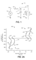
FIG. 1 is a schematic diagram of a circuit according to one example; -
FIG. 2A is a signal response curve illustrating characteristics of a device of the circuit ofFIG. 1 ; -
FIG. 2B is signal response curve illustrating negative differential resistance of a device of the circuit ofFIG. 1 ; -
FIG. 3 is a signal timing diagram illustrating operations of the circuit ofFIG. 1 ; -
FIG. 4 is a schematic diagram of a circuit according to another example; -
FIG. 5 is a schematic diagram of a circuit according to yet another example; -
FIG. 6 is a signal timing diagram illustrating operations of the circuit ofFIG. 4 ; -
FIG. 7 is a signal timing diagram illustrating other operations of the circuit ofFIG. 4 ; -
FIG. 8 is a signal timing diagram illustrating still other operations of the circuit ofFIG. 4 . - Circuitry and apparatus are provided that closely emulate biological neural responses. Two astable multivibrator circuits are coupled in series-circuit relationship. Each astable multivibrator circuit includes a negative differential resistance (NDR) device. Additionally, each of the astable multivibrator circuits is characterized by a distinct voltage-dependant time constant. The overall circuitry exhibits oscillations in electrical current when subjected to a voltage equal to or greater than a threshold value. Various oscillating waveforms can be produced in accordance with voltages applied to the circuitry.
- In one embodiment, an electronic circuit includes a first portion having a first current-controlled NDR device and a first capacitor coupled in parallel-circuit relationship. The first portion is coupled between a first node and a second node of the electronic circuit. The first portion is defined by a first voltage-dependant time constant. The electronic circuit also includes a second portion having a second current-controlled NDR device and a second capacitor coupled in parallel-circuit relationship. The second portion is coupled between the second node and a third node of the electronic circuit. The second portion is defined by a second voltage-dependant time constant that is different than the first voltage-dependant time constant.
- In another embodiment, an apparatus includes an electronic circuit. The electronic circuit includes a first astable multivibrator coupled between a first node and a second node. The first astable multivibrator includes a first NDR device. Additionally, the first astable multivibrator is characterized by a first voltage-dependent time constant. The electronic circuit also includes a second astable multivibrator coupled between the second node and a third node. The second astable multivibrator includes a second NDR device. The second astable multivibrator is characterized by a second voltage-dependent time constant that is different than the first voltage-dependent time constant. The electronic circuit is characterized by spike-like oscillations in an electrical current through the first and second astable multivibrators when an electrical potential equal to or greater than a threshold value is present between the first and third nodes.
- Reference is now directed to
FIG. 1 , which depicts a schematic diagram of acircuit 100. Thecircuit 100 is illustrative and non-limiting with respect to the present teachings. Thus, other circuits, devices or systems can be configured and/or operated in accordance with the present teachings. - The
circuit 100 includes a current-controlled negativedifferential resistance device 102, referred to hereinafter as an NDR device (or device) 102 in the interest of brevity. In one or more examples, the NDRdevice 102 is defined by a NDR memory resistor or “memristor”. The NDRdevice 102 is characterized by a switchable non-volatile resistance as well as negative differential resistance. Further discussion of NDR is provided below. - The electrical resistance of the
device 102 is selective adjustable by way of applied direct-current (DC) voltages. That is, the electrical resistance of thedevice 102 can be increased or decreased along a respective response curve by way of corresponding DC potentials. Additional information regarding current-controlled NDR devices and memristors contemplated for use with the present teachings can be found in U.S. patent application Ser. No. 12/837,903, titled “Memristive Negative Differential Resistance Device”, as filed 16 Jul. 2010, and naming Matthew D. Pickett as inventor, and which is incorporated herein in its entirety by reference. - The
circuit 100 also includes acapacitor 104. In one illustrative and non-limiting example, thecapacitor 104 is defined by a capacitance of one picoFarad (i.e., 1×10⁻¹² Farads). Other capacitors can also be used. Thecapacitor 104 is coupled in parallel-circuit relationship with thedevice 102 such that anRC stage 106 is defined. TheRC stage 106 is characterized by a voltage-dependent time constant. Thecircuit 100 is therefore characterized by a voltage-dependant time constant that varies in accordance with an applied DC potential. - The
circuit 100 also includes aresistor 108 coupled in series-circuit relationship with theRC stage 106. In one non-limiting example, theresistor 108 is defined by a resistance of ten kiloOhms (i.e., 10×103 Ohms). Other resistors can also be used. In yet one or more other examples, theresistor 108 is omitted. Thecircuit 100 further includes a source ofelectrical energy 110. In one example, theenergy source 110 is defined by a controllable or variable source of DC voltage. In another example, theenergy source 110 is defined by a constant or variable source of DC current. The energy source is coupled between anode 112 and anode 114. Typical normal operations of thecircuit 100 are described hereinafter. - Table 1 below includes illustrative and non-limiting examples of constituents of the
circuit 100. Other suitable values or elements can also be used in accordance with the present teachings: -
TABLE 1 Illustrative Circuit 100Element Value/Identity Notes/ Source NDR Device 102 Memristive NDR See U.S. 12/837,903 Capacitor 1041.0 pF (any source) Resistor 10810.0 kOhms (any source) Energy Source 110Variable Current (any source) -
FIG. 2A is a signal diagram depicting a voltage drop “Vout” versus current “I”response curve 200 corresponding to thedevice 102 of thecircuit 100. Voltage drop “Vout” across and current “I” through thedevice 102 are depicted inFIG. 1 for reference. Theresponse curve 200 is illustrative and non-limiting in accordance with the present teachings. Thus, other embodiments characterized by other response curves are also contemplated by the present teachings. - The
response curve 200 includes aportion 202. Theportion 202 depicts current flow ‘I’ through thedevice 102 corresponding to voltage drops “Vout” of positive polarity. In particular, an increasing applied voltage results in about zero current flow up to apoint 204, where after current begins to flow along theresponse curve 200 toward apoint 206. Beyond thepoint 206, the current “I” switches or “folds back” along theresponse curve 200 toward apoint 208. Thedevice 102 therefore exhibits hysteresis, switching between a “low resistance”operating region 210 and a “high resistance”operating region 212. - Some of the
portion 202 is below a memristive switchingcurrent threshold level 214. At least some normal operations according to the present teachings are performed at current levels having an absolute value less than theNDR threshold level 214. As long as the current “I” is maintained below thethreshold level 214, thedevice 102 will exhibit NDR but no memristive switching. If the absolute value of the current “I” is brought above thethreshold level 214, the memristance of thedevice 102 will change in a nonvolatile fashion. - The
response curve 200 also includes aportion 216. Theportion 216 depicts current flow through thedevice 102 corresponding to voltage drops “Vout” of negative polarity. In particular, a decreasing (i.e., more negative) applied voltage results in about zero current flow up to apoint 218, where after current begins to flow along theresponse curve 200 toward apoint 220. Beyond thepoint 220, the current switches or “folds back” along theresponse curve 200 toward apoint 222. Thedevice 102 switches between a “low resistance”operating region 224 and a “high resistance”operating region 226. - Some of the
portion 216 is below (of lesser absolute value than) a memristive switchingcurrent threshold level 228. Some normal operations according to the present teachings are performed at current values having an absolute value greater than theNDR threshold level 228. At least some normal operations according to the present teachings are performed at current levels having an absolute value less than theNDR threshold level 228. As long as the current “I” is maintained below thethreshold level 228, thedevice 102 will exhibit NDR but no memristive switching. - If the absolute value of the current “I” is brought above (of greater absolute value than) the
threshold level 228, the memristance of thedevice 102 will change in a nonvolatile fashion. Theresponse curve 200 described above corresponds to behavior exhibited by adevice 102 as contemplated by the present teachings. Thisdevice 102 behavior is germane to other circuit examples, operations and aspects of the present teachings as described below. - Attention is now directed to
FIG. 2B , which is a signal diagram depicting voltage drop “Vout” versus current “I”response curve 250 corresponding to theNDR device 102 of thecircuit 100. Theresponse curve 250 is non-limiting in accordance with the present teachings, and is illustrative of negative differential resistance of thedevice 102. Other embodiments characterized by other NDR response curves are also contemplated by the present teachings. - The
response curve 250 includes aportion 252. Theportion 252 depicts current flow “I” through theNDR device 102 and corresponding voltage drop “Vout” of positive polarity. In particular, an increasing current “I” corresponds to an increasing voltage drop “Vout” in a one-to-one manner, up to apoint 254. For current “I” of greater value, the voltage drop “Vout” exhibits a “fold back” or negative resistance characteristic up to about apoint 256. - The
response curve 250 includes anotherportion 258. Theportion 258 depicts current flow “I” through theNDR device 102 and corresponding voltage drop “Vout” of negative polarity. In particular, an increasing current “I” corresponds to an increasingly negative voltage drop “Vout” in a one-to-one manner, up to apoint 260. For current “I” of greater value, the voltage drop “Vout” exhibits a “fold back” or negative resistance characteristic up to about apoint 262. - Attention is now directed to
FIG. 3 , which depicts a signal timing diagram 300 according to one example of the present teachings. The signal timing diagram 300 depicts operations of thecircuit 100. The diagram 300 is illustrative and nonlimiting in nature. Other signal timing diagrams, corresponding to other circuits and their respective operations, are contemplated by the present teachings. - The diagram 300 depicts an electrical current “I” through and voltage drop Vout across the
NDR device 102 of thecircuit 100 with respect to time. The instantaneous value of current “I” is determined by reference to a left-sidevertical scale 302. The corresponding instantaneous voltage drop “Vout” across thedevice 102 is determined by reference to a right-sidevertical scale 304. - The diagram 300 includes a
portion 306 wherein the voltage drop “Vout” is of lesser absolute magnitude than athreshold value 308. Notably, thecircuit 100 exhibits no oscillations in either the current “I” or the corresponding voltage drop “Vout” in theportion 306. Thus, thecircuit 100 is characterized by a first operating mode wherein no oscillations in current “I” are exhibited. The first operating mode corresponds to applied voltages from thevoltage source 110 that are lesser in absolute magnitude than thethreshold value 308. - The diagram 300 also includes a
portion 310 wherein the voltage drop “Vout” is of equal or greater absolute magnitude than thethreshold value 308. Thecircuit 100 exhibits spike-like oscillations in the current “I” and the corresponding voltage drop “Vout” in theportion 310. Thecircuit 100 is therefore characterized by a second operating mode wherein thecircuit 100 behaves as an astable multivibrator or oscillator. - The second operating mode corresponds to applied voltages from the
voltage source 110 that are equal to or greater in absolute magnitude than thethreshold value 308. It is also noted that the oscillations increase in frequency in response to increased absolute value of the voltage applied to thecircuit 100. This increasing frequency of oscillations in the current “I” is depicted in aportion 312 of the diagram 300. - The diagram 300 is illustrative of normal operations of the
circuit 100 according to the present teachings. In general, and without limitation, circuits are contemplated by the present teachings that include an NDR device coupled in parallel-circuit relationship with a capacitor. The corresponding “RC” stage is characterized by a voltage-dependent time constant in accordance with the NDR behavior of the device. Circuits, such ascircuit 100 for non-limiting example, exhibit a non-oscillating operating mode and an oscillating operating mode, respectively, in accordance with the magnitude of a voltage applied thereto. Switchover from one operating mode to the other—and back again—occurs in accordance with an applied voltage threshold value exhibited by the particular circuit. - Attention is now directed to
FIG. 4 , which depicts a schematic view of acircuit 400 according to the present teachings. Thecircuit 400 is illustrative and non-limiting with respect to the present teachings. Thus, other circuits, devices or systems can be configured and/or operated in accordance with the present teachings. - The
circuit 400 includes afirst stage 402. Thefirst stage 402 includes anNDR device 404 coupled in parallel-circuit relationship with acapacitor 406. Thedevice 404 is characterized by negative differential resistance analogous to that described above. However, it is noted that particular electrical parameters can vary between NDR devices as contemplated herein. Thefirst stage 402 is also referred to as afirst multivibrator 402. In one or more examples, thedevice 404 is defined by a current-controlled NDR memristor. - The
first multivibrator 402 is characterized by a first voltage-dependant time constant in accordance with the particular electrical characteristics of thedevice 404 andcapacitor 406. Thefirst multivibrator 402 is also characterized by respective no-oscillating and oscillating operating modes in accordance with an applied voltage-threshold value. - The
circuit 400 also includes asecond stage 408. Thesecond stage 408 includes anNDR device 410 coupled in parallel-circuit relationship with acapacitor 412. Thedevice 410 is characterized by negative differential resistance analogous to that described above. Again, particular electrical parameters can vary between devices as contemplated herein. Thesecond stage 408 is also referred to as asecond multivibrator 408. In one or more examples, thedevice 410 is defined by a current-controlled NDR memristor. - The
second multivibrator 408 is characterized by a second voltage-dependant time constant in accordance with the particular electrical characteristics of thedevice 410 andcapacitor 412. Thesecond multivibrator 408 is also characterized by respective no-oscillating and oscillating operating modes in accordance with an applied voltage-threshold value. - The
circuit 400 also includes aresistor 414 coupled in series with the first andsecond multivibrators resistor 414 is omitted. Thecircuit 400 further includes a source of electrical energy orenergy source 416 coupled between anode 418 and anode 420. In one example, theenergy source 416 is defined by a controllable or variable source of DC voltage. In another example, theenergy source 416 is defined by a constant or variable source of DC current. Thus, the source ofelectrical energy 416 can be suitably selected in accordance with the operating goals of thecircuit 400. - The
first multivibrator 402 is coupled in series-circuit relationship with thesecond multivibrator 408. In this way, the operating modes of the first andsecond stages respective capacitors respective NDR devices first multivibrator 402 is characterized by a time constant of one microsecond at an applied voltage “Vin” of one volt, while thesecond multivibrator 408 is characterized by a time constant of ten microseconds at an applied voltage “Vin” of one volt. - The
illustrative circuit 400 is characterized by a number of operating modes by virtue of the distinct first and second voltage-dependant time constants and the interactive nature of the first andsecond multivibrators - Attention is turned to
FIG. 5 , which depicts a schematic view of acircuit 500 according to the present teachings. Thecircuit 500 is illustrative and non-limiting with respect to the present teachings. Thus, other circuits, devices or systems can be configured and/or operated in accordance with the present teachings. - The
circuit 500 includes afirst stage 502. Thefirst stage 502 includes anNDR device 504 coupled in series-circuit relationship with aresistor 506. In turn, thedevice 504 and theresistor 506 are coupled in parallel-circuit relationship with acapacitor 508. Thedevice 504 is characterized by negative differential resistance analogous to that described above. Particular electrical parameters can vary between NDR devices as contemplated herein. - The
first stage 502 is also referred to as afirst multivibrator 502. Thefirst multivibrator 502 is characterized by a first voltage-dependant time constant in accordance with the particular electrical characteristics of thedevice 504, theresistor 506 and thecapacitor 508. Thefirst multivibrator 502 exhibits respective no-oscillating and oscillating operating modes in accordance with an applied voltage-threshold value. - The
circuit 500 also includes asecond stage 510. Thesecond stage 510 includes anNDR device 512 coupled in series-circuit relationship with aresistor 514. Thedevice 512 andresistor 514 are coupled in parallel-circuit relationship with acapacitor 516. Thedevice 512 is characterized by negative differential resistance analogous to that described above. Thesecond stage 510 is also referred to as asecond multivibrator 510. - The
second multivibrator 510 is characterized by a second voltage-dependant time constant in accordance with the particular electrical characteristics of theNDR device 512, theresistor 514 and thecapacitor 516. Thesecond multivibrator 510 is characterized by respective no-oscillating and oscillating operating modes in accordance with an applied voltage-threshold value. - The
circuit 500 also includes aresistor 518 coupled in series with the first andsecond multivibrators resistor 518 is omitted. Thecircuit 500 further includes a source ofelectrical energy 520. Theenergy source 520 can be defined by a controllable or variable source of DC voltage, or a constant or variable source of DC current. The energy source is coupled between anode 522 and anode 524. - The
first multivibrator 502 is coupled in series-circuit relationship with thesecond multivibrator 510 such that respective operating modes are interactive. In one or more examples, therespective resistors capacitors NDR devices - The
circuit 500 is characterized by a number of operating modes analogous to those described below with respect to thecircuit 400. Additionally, thecircuit 500 illustrates at least one circuit variation contemplated by the present teachings by virtue of theresistors - Attention turned to
FIG. 6 , which depicts a signal timing diagram 600 according to one example of the present teachings. The signal timing diagram (diagram) 600 corresponds to operations of thecircuit 400. The diagram 600 is illustrative and non-limiting in nature. Other signal timing diagrams, corresponding to other circuits and their respective operations, are contemplated by the present teachings. - The diagram 600 depicts an electrical current “I2” through the
circuit 400 with respect to time. The instantaneous value of current “I2” is determined by reference to a left-sidevertical scale 602. An applied voltage “Vin”, as applied betweennodes vertical scale 604. - The diagram 600 depicts the applied voltage “Vin” beginning in time at or about zero volts and then making a transition to a constant value of one volt at about time zero-point-one milliseconds. In this illustration, a “Vin” value of one volt corresponds to the threshold value for the
circuit 400. That is, therespective multivibrators circuit 400 is subjected to one or more volts of applied potential betweennodes - In response, the current “I2” transitions from a zero value to a value of about twenty-five microamperes, lagging the applied voltage “Vin” slightly in time. The current “I2” is thereafter characterized by spike-like oscillations in value between about twenty-five microamperes and about ninety microamperes. The frequency of the oscillations in current “I2” is about constant in correspondence to the constant value of the applied voltage “Vin”. The oscillations in current “I2” result in corresponding oscillations in respective voltage drops “Vout1” and “Vout2”.
- One or both of the respective voltage drops “Vout1” and “Vout2” can be detected by other electronic circuitry (not shown) and amplified, digitally quantified, filtered, and so on, in accordance with any number of contemplated usages. Similarly, the
circuit 500 can be operated essentially as described above wherein a current “I3” can be detected by way of corresponding voltage drops “Vout3” and/or “Vout4”. - The diagram 600 depicts one illustrative mode of operation of the
circuit 400 according to the present teachings. Thecircuit 400 exhibits behavior that is notably similar to that of a mammalian olfactory neural response. Specifically, an applied voltage “Vin” equal to a threshold value results in spike-like oscillations in current “I2” of about constant frequency. These spike-like current oscillations are analogous to “trigger action” or transmitter release in an olfactory sensory neuron subjected to odorant concentration at a threshold detection level. Additionally, memristive characteristics within the circuit 400 (i.e.,NDR device 404 and/or 410) results in behavior similar to that of biological synaptic response. - Attention is directed to
FIG. 7 , which depicts a signal timing diagram 700 according to one example of the present teachings. The signal timing diagram (diagram) 700 corresponds to operations of thecircuit 400. The diagram 700 is illustrative and non-limiting in nature. Other signal timing diagrams, corresponding to other circuits and their respective operations, are contemplated by the present teachings. - The diagram 700 depicts an electrical current “I2” through the
circuit 400 with respect to time. The instantaneous value of current “I2” is determined by reference to a left-sidevertical scale 702. An applied voltage “Vin”, as applied betweennodes vertical scale 704. - The diagram 700 depicts the applied voltage “Vin” beginning at or about zero volts, and then making a transition to a constant value of about one-point-two volts just after time zero-point-zero milliseconds. In this illustration, a “Vin” value of one volt corresponds to the threshold value for the
circuit 400. Thus, the applied voltage “Vin” has exceeded the threshold value. - In response, the current “I2” transitions from a zero value to a value of about twenty-five microamperes and immediately thereafter exhibits spike-like oscillations in value between about twenty-five microamperes and about ninety microamperes. The frequency of the oscillations in current “I2” are initially relatively high during a
time period 706, decreasing toward a steady-state frequency during atime period 708 thereafter. - Thus, the diagram 700 depicts an operating mode for the
circuit 400 characterized by an initial transient in current “I2” oscillation frequency due to the greater-than-threshold value of the applied voltage “Vin”. In turn, the eventual steady-state value in current “I2” oscillation frequency corresponds to the constant value of the applied voltage “Vin”. - The oscillations in current “I2” result in corresponding oscillations in respective voltage drops “Vout1” and “Vout2”. The
circuit 500 can be operated essentially as described above, wherein current “I3” can be detected by way of voltage drops “Vout3” and/or “Vout4”. The diagram 700 depicts another illustrative mode of operation of thecircuit 400 according to the present teachings. In particular, an applied voltage “Vin” greater than a threshold value results in spike-like oscillations in current “I2” having a transitory frequency. - Attention is directed to
FIG. 8 , which depicts a signal timing diagram 800 according to one example of the present teachings. The signal timing diagram 800 corresponds to operations of thecircuit 400. The diagram 800 is illustrative and non-limiting in nature. Other signal timing diagrams, corresponding to other circuits and their respective operations, are contemplated by the present teachings. - The diagram 800 depicts an electrical current “I2” through the
circuit 400 with respect to time. The instantaneous value of current “I2” is determined by reference to a left-sidevertical scale 802. An applied voltage “Vin”, as applied betweennodes vertical scale 804. - The diagram 800 depicts the applied voltage “Vin” beginning at or about zero volts, and then making a transition to a constant value of about zero-point-nine-five volts just after time zero-point-zero milliseconds and extending to time zero-point-four milliseconds. In this illustration, a “Vin” value of one volt corresponds to the threshold value for the
circuit 400. Thus, the applied voltage “Vin” is slightly lesser than the threshold value. - In response, the current “I2” transitions from a zero value to about twenty-five microamperes and maintains that value consistently up to about time zero-point-four milliseconds, depicted as an
initial period 806. The constant, non-oscillating value of current “I2” is due to the slightly lesser than threshold value of the applied voltage “Vin”. - Thereafter, the applied voltage “Vin” exhibits a
voltage pulse 808 peaking at about one-point-two volts, and then transitioning back to the original value of about zero-point-nine-five volts. In response, the current “I2” is triggered into oscillations, swinging in amplitude between about twenty-five microamperes and about ninety-five microamperes. The oscillations of the current “I2” continue at about a constant frequency thereafter during aperiod 810. - The diagram 800 depicts an operating mode for the
circuit 400 characterized by an initial transient in current “I2” toward a non-oscillating, steady-state value due to the lesser-than-threshold value of the applied voltage “Vin”. Another operating mode is then initiated, or triggered, in response to a voltage pulse greater than the threshold value. The oscillations in current “I2” are sustained despite the reduction of applied voltage “Vin” to a value lesser than the threshold value. - The oscillations in current “I2” result in corresponding oscillations in respective voltage drops “Vout1” and “Vout2”. The
circuit 500 can be operated essentially as described above, wherein current “I3” can be detected by way of voltage drops “Vout3” and/or “Vout4”. The diagram 800 depicts another illustrative mode of operation of thecircuit 400 according to the present teachings. - In general, the foregoing description is intended to be illustrative and not restrictive. Many embodiments and applications other than the examples provided would be apparent to those of ordinary skill in the art upon reading the above description. The scope of the invention should be determined, not with reference to the above description, but should instead be determined with reference to the appended claims, along with the full scope of equivalents to which such claims are entitled. It is anticipated and intended that future developments will occur in the arts discussed herein, and that the disclosed systems and methods will be incorporated into such future embodiments. In sum, it should be understood that the invention is capable of modification and variation and is limited only by the following claims.
Claims (15)
Priority Applications (1)
| Application Number | Priority Date | Filing Date | Title |
|---|---|---|---|
| US13/078,595 US8324976B2 (en) | 2011-04-01 | 2011-04-01 | Oscillator circuitry having negative differential resistance |
Applications Claiming Priority (1)
| Application Number | Priority Date | Filing Date | Title |
|---|---|---|---|
| US13/078,595 US8324976B2 (en) | 2011-04-01 | 2011-04-01 | Oscillator circuitry having negative differential resistance |
Publications (2)
| Publication Number | Publication Date |
|---|---|
| US20120249252A1 true US20120249252A1 (en) | 2012-10-04 |
| US8324976B2 US8324976B2 (en) | 2012-12-04 |
Family
ID=46926429
Family Applications (1)
| Application Number | Title | Priority Date | Filing Date |
|---|---|---|---|
| US13/078,595 Expired - Fee Related US8324976B2 (en) | 2011-04-01 | 2011-04-01 | Oscillator circuitry having negative differential resistance |
Country Status (1)
| Country | Link |
|---|---|
| US (1) | US8324976B2 (en) |
Cited By (9)
| Publication number | Priority date | Publication date | Assignee | Title |
|---|---|---|---|---|
| US20130300509A1 (en) * | 2012-05-09 | 2013-11-14 | Gwangju Institute Of Science And Technology | Frequency tuning apparatus, operating method thereof, and rf circuit including the frequency tuning apparatus |
| WO2018140539A1 (en) * | 2017-01-26 | 2018-08-02 | Hrl Laboratories, Llc | A scalable, stackable, and beol-process compatible integrated neuron circuit |
| US20190034789A1 (en) * | 2017-07-31 | 2019-01-31 | Hewlett Packard Enterprise Development Lp | Non-boolean analog mott memristor network |
| US10297751B2 (en) | 2017-01-26 | 2019-05-21 | Hrl Laboratories, Llc | Low-voltage threshold switch devices with current-controlled negative differential resistance based on electroformed vanadium oxide layer |
| US10600961B2 (en) * | 2017-07-27 | 2020-03-24 | Hrl Laboratories, Llc | Scalable and low-voltage electroforming-free nanoscale vanadium dioxide threshold switch devices and relaxation oscillators with current controlled negative differential resistance |
| CN111933197A (en) * | 2020-07-09 | 2020-11-13 | 中国科学院微电子研究所 | Method and circuit for processing detected signal |
| US20220253684A1 (en) * | 2019-11-18 | 2022-08-11 | Institute Of Microelectronics Of The Chinese Academy Of Sciences | Afferent neuron circuit and mechanoreceptive system |
| US11861488B1 (en) * | 2017-06-09 | 2024-01-02 | Hrl Laboratories, Llc | Scalable excitatory and inhibitory neuron circuitry based on vanadium dioxide relaxation oscillators |
| CN119496466A (en) * | 2024-10-28 | 2025-02-21 | 南京航空航天大学 | A composite memristor and a large frequency modulation oscillator device for electrochemical reaction in a liquid pool |
Families Citing this family (3)
| Publication number | Priority date | Publication date | Assignee | Title |
|---|---|---|---|---|
| US10700638B2 (en) | 2016-04-28 | 2020-06-30 | Hewlett Packard Enterprise Development Lp | Spike train generating circuit |
| US10153729B2 (en) | 2016-04-28 | 2018-12-11 | Hewlett Packard Enterprise Development Lp | Nano-scale oscillator exhibiting chaotic oscillation |
| WO2018175233A1 (en) | 2017-03-19 | 2018-09-27 | Purdue Research Foundation | Methods and materials systems for enhancing corrosion resistance of solid materials and corrosion resistant devices made therefrom |
Family Cites Families (3)
| Publication number | Priority date | Publication date | Assignee | Title |
|---|---|---|---|---|
| US3249891A (en) * | 1959-08-05 | 1966-05-03 | Ibm | Oscillator apparatus utilizing esaki diode |
| US3054071A (en) * | 1961-05-31 | 1962-09-11 | Gen Electric | Polarity-sensitive negative resistance oscillator with frequency shift |
| US8212621B2 (en) * | 2010-10-29 | 2012-07-03 | Hewlett-Packard Development Company, L.P. | Memristive programmable frequency source and method |
-
2011
- 2011-04-01 US US13/078,595 patent/US8324976B2/en not_active Expired - Fee Related
Cited By (14)
| Publication number | Priority date | Publication date | Assignee | Title |
|---|---|---|---|---|
| US20130300509A1 (en) * | 2012-05-09 | 2013-11-14 | Gwangju Institute Of Science And Technology | Frequency tuning apparatus, operating method thereof, and rf circuit including the frequency tuning apparatus |
| US10903277B2 (en) | 2017-01-26 | 2021-01-26 | Hrl Laboratories, Llc | Scalable, stackable, and BEOL-process compatible integrated neuron circuit |
| US10297751B2 (en) | 2017-01-26 | 2019-05-21 | Hrl Laboratories, Llc | Low-voltage threshold switch devices with current-controlled negative differential resistance based on electroformed vanadium oxide layer |
| CN110199390A (en) * | 2017-01-26 | 2019-09-03 | Hrl实验室有限责任公司 | Scalable, stackable and BEOL process-compatible integrated neuron circuits |
| US10541274B2 (en) | 2017-01-26 | 2020-01-21 | Hrl Laboratories, Llc | Scalable, stackable, and BEOL-process compatible integrated neuron circuit |
| WO2018140539A1 (en) * | 2017-01-26 | 2018-08-02 | Hrl Laboratories, Llc | A scalable, stackable, and beol-process compatible integrated neuron circuit |
| US11861488B1 (en) * | 2017-06-09 | 2024-01-02 | Hrl Laboratories, Llc | Scalable excitatory and inhibitory neuron circuitry based on vanadium dioxide relaxation oscillators |
| US10600961B2 (en) * | 2017-07-27 | 2020-03-24 | Hrl Laboratories, Llc | Scalable and low-voltage electroforming-free nanoscale vanadium dioxide threshold switch devices and relaxation oscillators with current controlled negative differential resistance |
| US20190034789A1 (en) * | 2017-07-31 | 2019-01-31 | Hewlett Packard Enterprise Development Lp | Non-boolean analog mott memristor network |
| US10885430B2 (en) * | 2017-07-31 | 2021-01-05 | Hewlett Packard Enterprise Development Lp | Non-Boolean analog Mott memristor network |
| US20220253684A1 (en) * | 2019-11-18 | 2022-08-11 | Institute Of Microelectronics Of The Chinese Academy Of Sciences | Afferent neuron circuit and mechanoreceptive system |
| US12406177B2 (en) * | 2019-11-18 | 2025-09-02 | Institute Of Microelectronics Of The Chinese Academy Of Sciences | Afferent neuron circuit and mechanoreceptive system |
| CN111933197A (en) * | 2020-07-09 | 2020-11-13 | 中国科学院微电子研究所 | Method and circuit for processing detected signal |
| CN119496466A (en) * | 2024-10-28 | 2025-02-21 | 南京航空航天大学 | A composite memristor and a large frequency modulation oscillator device for electrochemical reaction in a liquid pool |
Also Published As
| Publication number | Publication date |
|---|---|
| US8324976B2 (en) | 2012-12-04 |
Similar Documents
| Publication | Publication Date | Title |
|---|---|---|
| US8324976B2 (en) | Oscillator circuitry having negative differential resistance | |
| Cam et al. | A new floating memristance simulator circuit based on second generation current conveyor | |
| Buscarino et al. | Memristive chaotic circuits based on cellular nonlinear networks | |
| CN106537767B (en) | Limiting oscillator circuit | |
| US20090212826A1 (en) | Hysteresis comparator | |
| JPWO2010016167A1 (en) | Reference frequency generation circuit, semiconductor integrated circuit, electronic equipment | |
| CN105207481B (en) | A kind of loop compensation circuit and switching power circuit | |
| CN1822211B (en) | Memory | |
| Alharbi et al. | Memristor emulator based on single CCII | |
| KR102590453B1 (en) | Second order switched capacitor filter | |
| Mbarek et al. | An analysis of the dynamics of SPICE memristor model | |
| CN104579629B (en) | A kind of chaotic oscillating circuit based on titanium dioxide memristor | |
| CN107171650B (en) | Variable gain amplifier circuit | |
| JP6311241B2 (en) | Preamplifier circuit for capacitive transducer | |
| JP5193098B2 (en) | Impulse generation circuit | |
| CN111933197B (en) | Method and circuit for processing detected signal | |
| Lo et al. | Tunable waveform generators using single dual-current output OTAs | |
| Jiri et al. | A Full-Wave Rectifier Based on Memristive Systems | |
| Vavra et al. | An envelope detector based on Memristive systems | |
| Ghedira et al. | Dynamical resistive switching of a generic memristor model: Analysis and simulation | |
| CN210297639U (en) | A Voltage Controlled Tunable Multivibrator | |
| Hu et al. | Chaos in a charge-controlled memcapacitor circuit | |
| JP2010028496A (en) | Oscillation detection circuit | |
| KR102242636B1 (en) | Pulse-Width Modulation based sensor interface circuits | |
| JP6705681B2 (en) | CV conversion circuit |
Legal Events
| Date | Code | Title | Description |
|---|---|---|---|
| AS | Assignment |
Owner name: HEWLETT-PACKARD DEVELOPMENT COMPANY, L.P., TEXAS Free format text: ASSIGNMENT OF ASSIGNORS INTEREST;ASSIGNORS:BORGHETTI, JULIEN;PICKETT, MATTHEW D.;RIBEIRO, GILBERTO MEDEIROS;AND OTHERS;REEL/FRAME:026063/0467 Effective date: 20110331 |
|
| ZAAA | Notice of allowance and fees due |
Free format text: ORIGINAL CODE: NOA |
|
| ZAAB | Notice of allowance mailed |
Free format text: ORIGINAL CODE: MN/=. |
|
| STCF | Information on status: patent grant |
Free format text: PATENTED CASE |
|
| CC | Certificate of correction | ||
| AS | Assignment |
Owner name: HEWLETT PACKARD ENTERPRISE DEVELOPMENT LP, TEXAS Free format text: ASSIGNMENT OF ASSIGNORS INTEREST;ASSIGNOR:HEWLETT-PACKARD DEVELOPMENT COMPANY, L.P.;REEL/FRAME:037079/0001 Effective date: 20151027 |
|
| FPAY | Fee payment |
Year of fee payment: 4 |
|
| MAFP | Maintenance fee payment |
Free format text: PAYMENT OF MAINTENANCE FEE, 8TH YEAR, LARGE ENTITY (ORIGINAL EVENT CODE: M1552); ENTITY STATUS OF PATENT OWNER: LARGE ENTITY Year of fee payment: 8 |
|
| FEPP | Fee payment procedure |
Free format text: MAINTENANCE FEE REMINDER MAILED (ORIGINAL EVENT CODE: REM.); ENTITY STATUS OF PATENT OWNER: LARGE ENTITY |
|
| LAPS | Lapse for failure to pay maintenance fees |
Free format text: PATENT EXPIRED FOR FAILURE TO PAY MAINTENANCE FEES (ORIGINAL EVENT CODE: EXP.); ENTITY STATUS OF PATENT OWNER: LARGE ENTITY |
|
| STCH | Information on status: patent discontinuation |
Free format text: PATENT EXPIRED DUE TO NONPAYMENT OF MAINTENANCE FEES UNDER 37 CFR 1.362 |
|
| FP | Lapsed due to failure to pay maintenance fee |
Effective date: 20241204 |