US20120249244A1 - Output buffer of source driver - Google Patents
Output buffer of source driver Download PDFInfo
- Publication number
- US20120249244A1 US20120249244A1 US13/435,322 US201213435322A US2012249244A1 US 20120249244 A1 US20120249244 A1 US 20120249244A1 US 201213435322 A US201213435322 A US 201213435322A US 2012249244 A1 US2012249244 A1 US 2012249244A1
- Authority
- US
- United States
- Prior art keywords
- output
- type transistor
- buffer
- coupled
- comparator
- Prior art date
- Legal status (The legal status is an assumption and is not a legal conclusion. Google has not performed a legal analysis and makes no representation as to the accuracy of the status listed.)
- Granted
Links
- 239000003990 capacitor Substances 0.000 claims abstract description 8
- 239000004973 liquid crystal related substance Substances 0.000 claims description 5
- 239000013256 coordination polymer Substances 0.000 description 21
- 238000010586 diagram Methods 0.000 description 8
- 230000000694 effects Effects 0.000 description 6
- 230000000007 visual effect Effects 0.000 description 5
- 230000004044 response Effects 0.000 description 3
- 230000035945 sensitivity Effects 0.000 description 2
- 102100031746 Bone sialoprotein 2 Human genes 0.000 description 1
- 101000707248 Homo sapiens Bone sialoprotein 2 Proteins 0.000 description 1
- 230000004075 alteration Effects 0.000 description 1
- 230000008901 benefit Effects 0.000 description 1
- 238000000034 method Methods 0.000 description 1
- 230000004048 modification Effects 0.000 description 1
- 238000012986 modification Methods 0.000 description 1
- 230000008569 process Effects 0.000 description 1
- 235000015096 spirit Nutrition 0.000 description 1
Images


Classifications
-
- H—ELECTRICITY
- H03—ELECTRONIC CIRCUITRY
- H03F—AMPLIFIERS
- H03F3/00—Amplifiers with only discharge tubes or only semiconductor devices as amplifying elements
- H03F3/45—Differential amplifiers
- H03F3/45071—Differential amplifiers with semiconductor devices only
- H03F3/45076—Differential amplifiers with semiconductor devices only characterised by the way of implementation of the active amplifying circuit in the differential amplifier
- H03F3/45179—Differential amplifiers with semiconductor devices only characterised by the way of implementation of the active amplifying circuit in the differential amplifier using MOSFET transistors as the active amplifying circuit
- H03F3/45183—Long tailed pairs
-
- G—PHYSICS
- G09—EDUCATION; CRYPTOGRAPHY; DISPLAY; ADVERTISING; SEALS
- G09G—ARRANGEMENTS OR CIRCUITS FOR CONTROL OF INDICATING DEVICES USING STATIC MEANS TO PRESENT VARIABLE INFORMATION
- G09G3/00—Control arrangements or circuits, of interest only in connection with visual indicators other than cathode-ray tubes
- G09G3/20—Control arrangements or circuits, of interest only in connection with visual indicators other than cathode-ray tubes for presentation of an assembly of a number of characters, e.g. a page, by composing the assembly by combination of individual elements arranged in a matrix no fixed position being assigned to or needed to be assigned to the individual characters or partial characters
- G09G3/34—Control arrangements or circuits, of interest only in connection with visual indicators other than cathode-ray tubes for presentation of an assembly of a number of characters, e.g. a page, by composing the assembly by combination of individual elements arranged in a matrix no fixed position being assigned to or needed to be assigned to the individual characters or partial characters by control of light from an independent source
- G09G3/36—Control arrangements or circuits, of interest only in connection with visual indicators other than cathode-ray tubes for presentation of an assembly of a number of characters, e.g. a page, by composing the assembly by combination of individual elements arranged in a matrix no fixed position being assigned to or needed to be assigned to the individual characters or partial characters by control of light from an independent source using liquid crystals
- G09G3/3611—Control of matrices with row and column drivers
- G09G3/3674—Details of drivers for scan electrodes
-
- G—PHYSICS
- G09—EDUCATION; CRYPTOGRAPHY; DISPLAY; ADVERTISING; SEALS
- G09G—ARRANGEMENTS OR CIRCUITS FOR CONTROL OF INDICATING DEVICES USING STATIC MEANS TO PRESENT VARIABLE INFORMATION
- G09G2310/00—Command of the display device
- G09G2310/02—Addressing, scanning or driving the display screen or processing steps related thereto
- G09G2310/0264—Details of driving circuits
- G09G2310/0291—Details of output amplifiers or buffers arranged for use in a driving circuit
Definitions
- the invention relates to driving circuit; in particular, to an output buffer applied in a source driver of a liquid crystal display.
- the driving apparatus of the TFT-LCD display mainly includes a source driving circuit and a gate driving circuit.
- the source driving circuit plays a very important role. Please refer to FIG. 1 .
- FIG. 1 illustrates a schematic diagram of a circuit structure of a conventional source driver.
- the source driver 1 includes a receiver 10 , a data register 12 , a bi-directional shift register 14 , a line latch 16 , a level shifter 18 , a digital-to-analog converter 20 , and an output buffer 22 .
- the main power domain of the source driver 1 includes digital power sources VDD, VSS and analog power sources AVDD, HAVDD, AGND.
- a plurality of output channels Y 1 ⁇ Yn of the source driver 1 can be divided into the even output channels and the odd output channels. If the output voltages of the even output channels are higher than HAVDD, the output voltages of the add output channels will be lower than HAVDD, and vice versa.
- This half analog power source structure of the TFT-LCD display can achieve the effect of saving system power consumption.
- the output buffer 22 of the source driver 1 is usually realized by an operational amplifier (OPAMP).
- OPAMP operational amplifier
- FIG. 2 illustrates a circuit diagram of a conventional operational amplifier POS with positive polarity operated under a half analog power source.
- the circuit of the operational amplifier POS includes a differential input stage DIS, bias current sources IBSP and IBSN, an output stage OS, a compensation capacitor C c , and a comparator CP.
- the operational amplifier POS with positive polarity is operated under the half analog power source, its input signal V in — POS , output signal V out — POS , and output stage OS have operation voltages between AVDD and HAVDD, and the comparator CP has an operation voltage between AVDD and AGND.
- the comparator CP can be realized by a cascading source follower, as shown in FIG. 3 .
- the NMOS transistor MN 1 will suffer body effect more serious than the PMOS transistor MP 1 and its threshold voltage will become larger. Therefore, the NMOS source follower will become less sensitive, and the response of the control signal Ctrl_P will be slower than the control signal Ctrl_N to cause the slew rate of output driving and sinking become unbalanced, and the visual performance of the TFT-LCD display will be seriously affected.
- the invention provides an output buffer applied in a source driver of a liquid crystal display to solve the above-mentioned problems occurred in the prior arts.
- An embodiment of the invention is an output buffer applied in a source driver of a liquid crystal display used for improving the unbalanced slew rate caused by the body effect of the source follower in prior arts to enhance the visual performance of the TFT-LCD display.
- the output buffer includes a buffer input, a buffer output, a differential input stage, a bias current source, an output stage, a compensation capacitor, and a comparator.
- the output stage and the comparator are both operated between an analog supply voltage (AVDD) and a half analog supply voltage (HAVDD), or both operated between the half analog supply voltage (HAVDD) and a ground voltage.
- the comparator compares an input signal with an output signal and outputs a control signal to the bias current source according to the compared result.
- FIG. 1 illustrates a schematic diagram of a circuit structure of a conventional source driver.
- FIG. 2 illustrates a circuit diagram of a conventional operational amplifier with positive polarity operated under a half analog power source.
- FIG. 3 illustrates an embodiment of the comparator shown in FIG. 2 .
- FIG. 4 illustrates a circuit diagram of an operational amplifier with positive polarity operated under a half analog power source.
- FIG. 5 illustrates an embodiment of the comparator shown in FIG. 4 .
- FIG. 6 illustrates a circuit diagram of a negative operational amplifier operated under a half analog power source.
- FIG. 7 illustrates an embodiment of the comparator shown in FIG. 6 .
- An embodiment of the invention is an output buffer.
- the output buffer is applied in a source driver of a TFT-LCD display, but not limited to this.
- the circuit structure of the source driver of the TFT-LCD display can be also referred in FIG. 1 .
- the source driver 1 includes a receiver 10 , a data register 12 , a bi-directional shift register 14 , a line latch 16 , a level shifter 18 , a digital-to-analog converter 20 , and an output buffer 22 .
- the receiver 10 is coupled to the data register 12 ; the data register 12 is coupled to the line latch 16 ; the bi-directional shift register 14 is coupled to the line latch 16 ; the line latch 16 is coupled to the level shifter 18 ; the level shifter 18 is coupled to the digital-to-analog converter 20 ; the digital-to-analog converter 20 is coupled to the output buffer 22 .
- the main power domain of the source driver 1 includes digital power sources VDD, VSS and analog power sources AVDD, HAVDD, AGND.
- AVDD represents the analog supply voltage
- HAVDD represents the half analog supply voltage
- AGND represents the ground voltage.
- a plurality of output channels Y 1 ⁇ Yn of the source driver 1 can be divided into even output channels and odd output channels. If the output voltages of the even output channels are higher than HAVDD, the output voltages of the add output channels will be lower than HAVDD, and vice versa.
- This half analog power source structure of the TFT-LCD display can achieve the effect of saving system power consumption.
- the output buffer 22 of the source driver 1 will be introduced in detail as follows.
- the output buffer 22 of the source driver 1 can be realized by an operational amplifier (OPAMP), but not limited to this.
- OPAMP operational amplifier
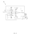
- FIG. 4 illustrates a circuit diagram of the operational amplifier POS with positive polarity operated under a half analog power source.
- the circuit of the operational amplifier POS includes a buffer input BI, a buffer output BO, a differential input stage DIS, two bias current sources I BSP and I BSN , an output stage OS, two compensation capacitors C c , and a comparator CP.
- the differential input stage DIS is coupled to the buffer input BI; the two bias current sources I BSP and I BSN are both coupled to the differential input stage DIS; the output stage OS is coupled between the differential input stage DIS and the buffer output BO; one end of the compensation capacitor C c is coupled between the differential input stage DIS and the output stage OS, and the other end of the compensation capacitor C c is coupled between the output stage OS and the buffer output BO; two comparator inputs CI 1 and CI 2 of the comparator CP are coupled to the buffer input BI and the buffer output BO respectively, and a comparator output CO of the comparator CP is coupled to the two bias current sources I BSP and I BSN .
- the bias current source I BSP is coupled between the differential input stage DIS and the analog operation voltage AVDD in series, and the current outputted from the bias current source I BSP flows toward the differential input stage DIS; the bias current source I BSN is coupled between the differential input stage DIS and the ground voltage AGND, and the current outputted from the bias current source I BSN flows toward the ground voltage AGND.
- the buffer input BI is used to receive the output signal V in — POS and transmit the output signal V in — POS to the differential input stage DIS. After the differential input stage DIS processes the input signal V in — POS , the differential input stage DIS transmits the processed input signal V in — POS to the output stage OS.
- the output signal V out — POS is outputted by the buffer output BO. Because the two comparator inputs CI 1 and CI 2 of the comparator CP are coupled to the buffer input BI and the buffer output BO respectively, the comparator CP can compare the input signal V in — POS with the output signal V out — POS and output a control signal through its comparator output CO to the two bias current sources I BSP and I BSN according to the compared result to control the current outputted from the two bias current sources I BSP and I BSN .
- the output stage OS of the operational amplifier POS with positive polarity is operated between the analog operation voltage AVDD and the half analog operation voltage HAVDD
- the comparator CP is also operated between the analog operation voltage AVDD and the half analog operation voltage HAVDD. This is obviously different from the feature that the operation voltage of the comparator CP is between the analog operation voltage AVDD and the ground voltage AGND in prior arts shown in FIG. 2 .
- the operational amplifier POS with positive polarity is operated under the half analog operation voltage HAVDD
- the input signal V in — POS , the output signal V out — POS , and the output stage OS will have operation voltages between the analog operation voltage AVDD and the half analog operation voltage HAVDD
- its comparator CP can be realized by a cascading source follower, but not limited to this.
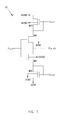
- FIG. 5 illustrates an embodiment of the comparator CP shown in FIG. 4 .
- the comparator CP is realized by a cascading source follower, but not limited to this.
- the comparator CP includes not only the two comparator inputs CI 1 , CI 2 , and the comparator output CO, but also a first N-type transistor MN 1 , a second N-type transistor MN 2 , a first P-type transistor MP 1 , and a second P-type transistor MP 2 .
- the first N-type transistor MN 1 and the second N-type transistor MN 2 can be NMOS transistors
- the first P-type transistor MP 1 and the second P-type transistor MP 2 can be PMOS transistors, but not limited to this.
- the first N-type transistor MN 1 is coupled to the half analog operation voltage HAVDD; the second N-type transistor MN 2 is coupled to the half analog operation voltage HAVDD; the first P-type transistor MP 1 is coupled between the first N-type transistor MN 1 and the second N-type transistor MN 2 , and coupled to the analog operation voltage AVDD; the second P-type transistor MP 2 is coupled between the first N-type transistor MN 1 and the analog operation voltage AVDD.
- the power domain of the base PB 1 of the first P-type transistor MP 1 is the analog supply voltage (AVDD), and the power domains of the base PB 2 and the source PS 2 of the second P-type transistor MP 2 are also the analog supply voltage (AVDD).
- the power domain of the base NB 1 of the first N-type transistor MN 1 is the half analog supply voltage (HAVDD), and the power domains of the base NB 2 and the source NS 2 of the second N-type transistor MN 2 are also the half analog supply voltage (HAVDD).
- the power domain of the base NB 1 of the first N-type transistor MN 1 is the ground voltage AGND and power domains of the base NB 2 and the source NS 2 of the second N-type transistor MN 2 are also the ground voltage AGND in prior arts shown in FIG. 3 .
- FIG. 6 illustrates a circuit diagram of the operational amplifier NOS with negative polarity operated under a half analog power source.
- the output stage OS of the operational amplifier NOS with negative polarity is operated between the half analog supply voltage (HAVDD) and the ground voltage (AGND)
- the comparator CP is operated between the half analog supply voltage (HAVDD) and the ground voltage (AGND).
- FIG. 7 illustrates an embodiment of the comparator CP shown in FIG. 6 .
- the comparator CP is realized by a cascading source follower, but not limited to this.
- the comparator CP includes not only the two comparator inputs CI 1 , CI 2 , and the comparator output CO, but also a first N-type transistor MN 1 , a second N-type transistor MN 2 , a first P-type transistor MP 1 , and a second P-type transistor MP 2 .
- the first N-type transistor MN 1 and the second N-type transistor MN 2 can be NMOS transistors
- the first P-type transistor MP 1 and the second P-type transistor MP 2 can be PMOS transistors, but not limited to this.
- FIG. 7 the difference between FIG. 7 and FIG. 5 is that the first N-type transistor MN 1 of FIG. 7 is coupled to the ground voltage AGND; the second N-type transistor MN 2 of FIG. 7 is coupled to the ground voltage AGND; the first P-type transistor MP 1 of FIG. 7 is coupled between the first N-type transistor MN 1 and the second N-type transistor MN 2 , and coupled to the half analog supply voltage (HAVDD); the second P-type transistor MP 2 of FIG. 7 is coupled between the first N-type transistor MN 1 and the half analog supply voltage (HAVDD).
- HAVDD half analog supply voltage
- the power domain of the base PB 1 of the first P-type transistor MP 1 of the comparator CP is the half analog supply voltage (HAVDD), and the power domains of the base PB 2 and the source PS 2 of the second P-type transistor MP 2 are also the half analog supply voltage (HAVDD).
- the power domain of the base NB 1 of the first N-type transistor MN 1 is the ground voltage (AGND), and the power domains of the base NB 2 and the source NS 2 of the second N-type transistor MN 2 are also the ground voltage (AGND).
Landscapes
- Engineering & Computer Science (AREA)
- Chemical & Material Sciences (AREA)
- Crystallography & Structural Chemistry (AREA)
- Physics & Mathematics (AREA)
- Computer Hardware Design (AREA)
- General Physics & Mathematics (AREA)
- Theoretical Computer Science (AREA)
- Power Engineering (AREA)
- Liquid Crystal Display Device Control (AREA)
- Control Of Indicators Other Than Cathode Ray Tubes (AREA)
- Amplifiers (AREA)
Abstract
Description
- 1. Field of the Invention
- The invention relates to driving circuit; in particular, to an output buffer applied in a source driver of a liquid crystal display.
- 2. Description of the Prior Art
- In recent years, with the continuous progress of display technology, various types of display apparatuses, such as a LCD display and a plasma display, are shown in the market. Because the volume of the LCD display is much smaller the conventional CRT display, the LCD display using smaller desk space is convenient for the people in modern life.
- In general, the driving apparatus of the TFT-LCD display mainly includes a source driving circuit and a gate driving circuit. For the TFT-LCD display having high quality, high resolution, and low power consumption, the source driving circuit plays a very important role. Please refer to
FIG. 1 .FIG. 1 illustrates a schematic diagram of a circuit structure of a conventional source driver. - As shown in
FIG. 1 , thesource driver 1 includes areceiver 10, adata register 12, abi-directional shift register 14, aline latch 16, alevel shifter 18, a digital-to-analog converter 20, and anoutput buffer 22. The main power domain of thesource driver 1 includes digital power sources VDD, VSS and analog power sources AVDD, HAVDD, AGND. In general, a plurality of output channels Y1˜Yn of thesource driver 1 can be divided into the even output channels and the odd output channels. If the output voltages of the even output channels are higher than HAVDD, the output voltages of the add output channels will be lower than HAVDD, and vice versa. This half analog power source structure of the TFT-LCD display can achieve the effect of saving system power consumption. - The
output buffer 22 of thesource driver 1 is usually realized by an operational amplifier (OPAMP). For thesource driver 1 of the TFT-LCD display, its visual performance is determined by the operational amplifier, especially the slew rate which is important to the TFT-LCD display applied in the high frame rate application. - Please refer to
FIG. 2 .FIG. 2 illustrates a circuit diagram of a conventional operational amplifier POS with positive polarity operated under a half analog power source. As shown inFIG. 2 , the circuit of the operational amplifier POS includes a differential input stage DIS, bias current sources IBSP and IBSN, an output stage OS, a compensation capacitor Cc, and a comparator CP. Because the operational amplifier POS with positive polarity is operated under the half analog power source, its input signal Vin— POS, output signal Vout— POS, and output stage OS have operation voltages between AVDD and HAVDD, and the comparator CP has an operation voltage between AVDD and AGND. And, the comparator CP can be realized by a cascading source follower, as shown inFIG. 3 . - As shown in
FIG. 3 , because the swing level of the input signal and output signal, the NMOS transistor MN1 will suffer body effect more serious than the PMOS transistor MP1 and its threshold voltage will become larger. Therefore, the NMOS source follower will become less sensitive, and the response of the control signal Ctrl_P will be slower than the control signal Ctrl_N to cause the slew rate of output driving and sinking become unbalanced, and the visual performance of the TFT-LCD display will be seriously affected. - Therefore, the invention provides an output buffer applied in a source driver of a liquid crystal display to solve the above-mentioned problems occurred in the prior arts.
- An embodiment of the invention is an output buffer applied in a source driver of a liquid crystal display used for improving the unbalanced slew rate caused by the body effect of the source follower in prior arts to enhance the visual performance of the TFT-LCD display.
- In this embodiment, the output buffer includes a buffer input, a buffer output, a differential input stage, a bias current source, an output stage, a compensation capacitor, and a comparator. The output stage and the comparator are both operated between an analog supply voltage (AVDD) and a half analog supply voltage (HAVDD), or both operated between the half analog supply voltage (HAVDD) and a ground voltage. The comparator compares an input signal with an output signal and outputs a control signal to the bias current source according to the compared result.
- The advantage and spirit of the invention may be understood by the following detailed descriptions together with the appended drawings.
-
FIG. 1 illustrates a schematic diagram of a circuit structure of a conventional source driver. -
FIG. 2 illustrates a circuit diagram of a conventional operational amplifier with positive polarity operated under a half analog power source. -
FIG. 3 illustrates an embodiment of the comparator shown inFIG. 2 . -
FIG. 4 illustrates a circuit diagram of an operational amplifier with positive polarity operated under a half analog power source. -
FIG. 5 illustrates an embodiment of the comparator shown inFIG. 4 . -
FIG. 6 illustrates a circuit diagram of a negative operational amplifier operated under a half analog power source. -
FIG. 7 illustrates an embodiment of the comparator shown inFIG. 6 . - An embodiment of the invention is an output buffer. In this embodiment, the output buffer is applied in a source driver of a TFT-LCD display, but not limited to this.
- In this embodiment, the circuit structure of the source driver of the TFT-LCD display can be also referred in
FIG. 1 . As shown inFIG. 1 , thesource driver 1 includes areceiver 10, adata register 12, abi-directional shift register 14, aline latch 16, alevel shifter 18, a digital-to-analog converter 20, and anoutput buffer 22. Wherein, thereceiver 10 is coupled to thedata register 12; thedata register 12 is coupled to theline latch 16; thebi-directional shift register 14 is coupled to theline latch 16; theline latch 16 is coupled to thelevel shifter 18; thelevel shifter 18 is coupled to the digital-to-analog converter 20; the digital-to-analog converter 20 is coupled to theoutput buffer 22. - It should be noticed that the main power domain of the
source driver 1 includes digital power sources VDD, VSS and analog power sources AVDD, HAVDD, AGND. Wherein, AVDD represents the analog supply voltage; HAVDD represents the half analog supply voltage; AGND represents the ground voltage. A plurality of output channels Y1˜Yn of thesource driver 1 can be divided into even output channels and odd output channels. If the output voltages of the even output channels are higher than HAVDD, the output voltages of the add output channels will be lower than HAVDD, and vice versa. This half analog power source structure of the TFT-LCD display can achieve the effect of saving system power consumption. - Since the operations and functions of the
receiver 10, thedata register 12, thebi-directional shift register 14, theline latch 16, thelevel shifter 18, and the digital-to-analog converter 20 are the same with those in prior arts, and they will not be described again here. Next, the most important technology feature of the invention, theoutput buffer 22 of thesource driver 1, will be introduced in detail as follows. - In this embodiment, the
output buffer 22 of thesource driver 1 can be realized by an operational amplifier (OPAMP), but not limited to this. Please refer toFIG. 4 .FIG. 4 illustrates a circuit diagram of the operational amplifier POS with positive polarity operated under a half analog power source. As shown inFIG. 4 , the circuit of the operational amplifier POS includes a buffer input BI, a buffer output BO, a differential input stage DIS, two bias current sources IBSP and IBSN, an output stage OS, two compensation capacitors Cc, and a comparator CP. - Wherein, the differential input stage DIS is coupled to the buffer input BI; the two bias current sources IBSP and IBSN are both coupled to the differential input stage DIS; the output stage OS is coupled between the differential input stage DIS and the buffer output BO; one end of the compensation capacitor Cc is coupled between the differential input stage DIS and the output stage OS, and the other end of the compensation capacitor Cc is coupled between the output stage OS and the buffer output BO; two comparator inputs CI1 and CI2 of the comparator CP are coupled to the buffer input BI and the buffer output BO respectively, and a comparator output CO of the comparator CP is coupled to the two bias current sources IBSP and IBSN.
- In this embodiment, the bias current source IBSP is coupled between the differential input stage DIS and the analog operation voltage AVDD in series, and the current outputted from the bias current source IBSP flows toward the differential input stage DIS; the bias current source IBSN is coupled between the differential input stage DIS and the ground voltage AGND, and the current outputted from the bias current source IBSN flows toward the ground voltage AGND. The buffer input BI is used to receive the output signal Vin
— POS and transmit the output signal Vin— POS to the differential input stage DIS. After the differential input stage DIS processes the input signal Vin— POS, the differential input stage DIS transmits the processed input signal Vin— POS to the output stage OS. After the output stage OS converts the input signal Vin— POS into the output signal Vout— POS, the output signal Vout— POS is outputted by the buffer output BO. Because the two comparator inputs CI1 and CI2 of the comparator CP are coupled to the buffer input BI and the buffer output BO respectively, the comparator CP can compare the input signal Vin— POS with the output signal Vout— POS and output a control signal through its comparator output CO to the two bias current sources IBSP and IBSN according to the compared result to control the current outputted from the two bias current sources IBSP and IBSN. - As shown in
FIG. 4 , in this embodiment, it should be noticed that the output stage OS of the operational amplifier POS with positive polarity is operated between the analog operation voltage AVDD and the half analog operation voltage HAVDD, and the comparator CP is also operated between the analog operation voltage AVDD and the half analog operation voltage HAVDD. This is obviously different from the feature that the operation voltage of the comparator CP is between the analog operation voltage AVDD and the ground voltage AGND in prior arts shown inFIG. 2 . - Because the operational amplifier POS with positive polarity is operated under the half analog operation voltage HAVDD, the input signal Vin
— POS, the output signal Vout— POS, and the output stage OS will have operation voltages between the analog operation voltage AVDD and the half analog operation voltage HAVDD, and its comparator CP can be realized by a cascading source follower, but not limited to this. - Then, Please refer to
FIG. 5 .FIG. 5 illustrates an embodiment of the comparator CP shown inFIG. 4 . As shown inFIG. 5 , the comparator CP is realized by a cascading source follower, but not limited to this. In this embodiment, the comparator CP includes not only the two comparator inputs CI1, CI2, and the comparator output CO, but also a first N-type transistor MN1, a second N-type transistor MN2, a first P-type transistor MP1, and a second P-type transistor MP2. In fact, the first N-type transistor MN1 and the second N-type transistor MN2 can be NMOS transistors, and the first P-type transistor MP1 and the second P-type transistor MP2 can be PMOS transistors, but not limited to this. - Wherein, the first N-type transistor MN1 is coupled to the half analog operation voltage HAVDD; the second N-type transistor MN2 is coupled to the half analog operation voltage HAVDD; the first P-type transistor MP1 is coupled between the first N-type transistor MN1 and the second N-type transistor MN2, and coupled to the analog operation voltage AVDD; the second P-type transistor MP2 is coupled between the first N-type transistor MN1 and the analog operation voltage AVDD.
- As shown in
FIG. 5 , in this embodiment, it should be noticed that the power domain of the base PB1 of the first P-type transistor MP1 is the analog supply voltage (AVDD), and the power domains of the base PB2 and the source PS2 of the second P-type transistor MP2 are also the analog supply voltage (AVDD). The power domain of the base NB1 of the first N-type transistor MN1 is the half analog supply voltage (HAVDD), and the power domains of the base NB2 and the source NS2 of the second N-type transistor MN2 are also the half analog supply voltage (HAVDD). This is obviously different from the feature that the power domain of the base NB1 of the first N-type transistor MN1 is the ground voltage AGND and power domains of the base NB2 and the source NS2 of the second N-type transistor MN2 are also the ground voltage AGND in prior arts shown inFIG. 3 . - In this condition, if the absolute values of the threshold voltages of the first N-type transistor MN1 and the first P-type transistor MP1 are similar, the body effects acted on the first N-type transistor MN1 and the first P-type transistor MP1 are also similar. Therefore, the source followers of the comparator CP can still maintain their sensitivities, and the responses of the control signals Ctrl_P and Ctrl_N will be identical, so that the slew rates of output driving and sinking will be balanced to reduce the unnecessary power consumption. By doing so, the problem of the unbalanced slew rates in prior arts can be overcome, and the visual performance of the TFT-LCD display can be also largely improved.
- Similarly, the above-mentioned ways can also applied in the operational amplifier NOS with negative polarity. Please refer to
FIG. 6 .FIG. 6 illustrates a circuit diagram of the operational amplifier NOS with negative polarity operated under a half analog power source. The difference betweenFIG. 4 andFIG. 6 is that the output stage OS of the operational amplifier NOS with negative polarity is operated between the half analog supply voltage (HAVDD) and the ground voltage (AGND), and the comparator CP is operated between the half analog supply voltage (HAVDD) and the ground voltage (AGND). - Then, Please refer to
FIG. 7 .FIG. 7 illustrates an embodiment of the comparator CP shown inFIG. 6 . As shown inFIG. 7 , the comparator CP is realized by a cascading source follower, but not limited to this. In this embodiment, the comparator CP includes not only the two comparator inputs CI1, CI2, and the comparator output CO, but also a first N-type transistor MN1, a second N-type transistor MN2, a first P-type transistor MP1, and a second P-type transistor MP2. In fact, the first N-type transistor MN1 and the second N-type transistor MN2 can be NMOS transistors, and the first P-type transistor MP1 and the second P-type transistor MP2 can be PMOS transistors, but not limited to this. - It should be noticed that the difference between
FIG. 7 andFIG. 5 is that the first N-type transistor MN1 ofFIG. 7 is coupled to the ground voltage AGND; the second N-type transistor MN2 ofFIG. 7 is coupled to the ground voltage AGND; the first P-type transistor MP1 ofFIG. 7 is coupled between the first N-type transistor MN1 and the second N-type transistor MN2, and coupled to the half analog supply voltage (HAVDD); the second P-type transistor MP2 ofFIG. 7 is coupled between the first N-type transistor MN1 and the half analog supply voltage (HAVDD). The power domain of the base PB1 of the first P-type transistor MP1 of the comparator CP is the half analog supply voltage (HAVDD), and the power domains of the base PB2 and the source PS2 of the second P-type transistor MP2 are also the half analog supply voltage (HAVDD). The power domain of the base NB1 of the first N-type transistor MN1 is the ground voltage (AGND), and the power domains of the base NB2 and the source NS2 of the second N-type transistor MN2 are also the ground voltage (AGND). - In this condition, if the absolute values of the threshold voltages of the first N-type transistor MN1 and the first P-type transistor MP1 are similar, the body effects acted on the first N-type transistor MN1 and the first P-type transistor MP1 are also similar. Therefore, the source followers of the comparator CP can still maintain their sensitivities, and the responses of the control signals Ctrl_P and Ctrl_N will be identical, so that the slew rates of output driving and sinking will be balanced to reduce the unnecessary power consumption. By doing so, the problem of the unbalanced slew rates in prior arts can be overcome, and the visual performance of the TFT-LCD display can be also largely improved.
- With the example and explanations above, the features and spirits of the invention will be hopefully well described. Those skilled in the art will readily observe that numerous modifications and alterations of the device may be made while retaining the teaching of the invention. Accordingly, the above disclosure should be construed as limited only by the metes and bounds of the appended claims.
Claims (10)
Applications Claiming Priority (3)
| Application Number | Priority Date | Filing Date | Title |
|---|---|---|---|
| TW100111232A | 2011-03-31 | ||
| TW100111232 | 2011-03-31 | ||
| TW100111232A TWI469518B (en) | 2011-03-31 | 2011-03-31 | Output buffer of source driver |
Publications (2)
| Publication Number | Publication Date |
|---|---|
| US20120249244A1 true US20120249244A1 (en) | 2012-10-04 |
| US8736372B2 US8736372B2 (en) | 2014-05-27 |
Family
ID=46926422
Family Applications (1)
| Application Number | Title | Priority Date | Filing Date |
|---|---|---|---|
| US13/435,322 Expired - Fee Related US8736372B2 (en) | 2011-03-31 | 2012-03-30 | Output buffer of source driver |
Country Status (3)
| Country | Link |
|---|---|
| US (1) | US8736372B2 (en) |
| CN (1) | CN102737594B (en) |
| TW (1) | TWI469518B (en) |
Cited By (5)
| Publication number | Priority date | Publication date | Assignee | Title |
|---|---|---|---|---|
| EP3038094A1 (en) * | 2014-12-22 | 2016-06-29 | LG Display Co., Ltd. | Source driver, display device with the same and driving method thereof |
| US9508303B2 (en) | 2013-05-30 | 2016-11-29 | Samsung Display Co., Ltd. | Display device |
| US10902791B2 (en) * | 2019-01-16 | 2021-01-26 | Novatek Microelectronics Corp. | Method of controlling source driver and related display system |
| US11205372B2 (en) * | 2019-09-23 | 2021-12-21 | Beijing Boe Display Technology Co., Ltd. | Source driving circuit, driving method and display device |
| US11462142B2 (en) * | 2020-12-14 | 2022-10-04 | Beijing Eswin Computing Technology Co., Ltd. | Slew rate boosting circuit, source driver chip and display device |
Citations (2)
| Publication number | Priority date | Publication date | Assignee | Title |
|---|---|---|---|---|
| US7567244B2 (en) * | 2005-04-06 | 2009-07-28 | Renesas Technology Corp. | Semiconductor integrated circuit for driving a liquid crystal display |
| US7821340B2 (en) * | 2008-08-08 | 2010-10-26 | Orise Technology Co., Ltd. | Output stage circuit and operational amplifier |
Family Cites Families (3)
| Publication number | Priority date | Publication date | Assignee | Title |
|---|---|---|---|---|
| US7852331B2 (en) * | 2005-11-14 | 2010-12-14 | Case Western Reserve University | High-voltage ternary driver using dynamic ground |
| JP5098395B2 (en) * | 2007-03-29 | 2012-12-12 | セイコーエプソン株式会社 | Electrophoretic display panel drive device, electrophoretic display device, and electronic apparatus |
| JP2009194485A (en) * | 2008-02-12 | 2009-08-27 | Nec Electronics Corp | Operational amplifier circuit and display |
-
2011
- 2011-03-31 TW TW100111232A patent/TWI469518B/en not_active IP Right Cessation
- 2011-04-18 CN CN201110103228.XA patent/CN102737594B/en not_active Expired - Fee Related
-
2012
- 2012-03-30 US US13/435,322 patent/US8736372B2/en not_active Expired - Fee Related
Patent Citations (2)
| Publication number | Priority date | Publication date | Assignee | Title |
|---|---|---|---|---|
| US7567244B2 (en) * | 2005-04-06 | 2009-07-28 | Renesas Technology Corp. | Semiconductor integrated circuit for driving a liquid crystal display |
| US7821340B2 (en) * | 2008-08-08 | 2010-10-26 | Orise Technology Co., Ltd. | Output stage circuit and operational amplifier |
Cited By (6)
| Publication number | Priority date | Publication date | Assignee | Title |
|---|---|---|---|---|
| US9508303B2 (en) | 2013-05-30 | 2016-11-29 | Samsung Display Co., Ltd. | Display device |
| EP3038094A1 (en) * | 2014-12-22 | 2016-06-29 | LG Display Co., Ltd. | Source driver, display device with the same and driving method thereof |
| US10217393B2 (en) | 2014-12-22 | 2019-02-26 | Lg Display Co., Ltd. | Source driver, display device with the same and driving method thereof |
| US10902791B2 (en) * | 2019-01-16 | 2021-01-26 | Novatek Microelectronics Corp. | Method of controlling source driver and related display system |
| US11205372B2 (en) * | 2019-09-23 | 2021-12-21 | Beijing Boe Display Technology Co., Ltd. | Source driving circuit, driving method and display device |
| US11462142B2 (en) * | 2020-12-14 | 2022-10-04 | Beijing Eswin Computing Technology Co., Ltd. | Slew rate boosting circuit, source driver chip and display device |
Also Published As
| Publication number | Publication date |
|---|---|
| CN102737594A (en) | 2012-10-17 |
| CN102737594B (en) | 2014-11-19 |
| TWI469518B (en) | 2015-01-11 |
| US8736372B2 (en) | 2014-05-27 |
| TW201240349A (en) | 2012-10-01 |
Similar Documents
| Publication | Publication Date | Title |
|---|---|---|
| US8736373B2 (en) | Output buffer of source driver | |
| CN101178883B (en) | Data driver and display device | |
| CN108091307B (en) | Output circuit and data driver of liquid crystal display device | |
| US8390609B2 (en) | Differential amplifier and drive circuit of display device using the same | |
| US8988402B2 (en) | Output circuit, data driver, and display device | |
| US9543912B2 (en) | Buffer circuit having an enhanced slew-rate and source driving circuit including the same | |
| KR101832491B1 (en) | Output circuit, data driver, and display device | |
| US8581894B2 (en) | Output circuit, data driver and display device | |
| KR102670564B1 (en) | Data driver and display apparatus including the same | |
| US10026375B2 (en) | Output amplifier of a source driver and control method thereof | |
| US20090040165A1 (en) | Amplifying circuit and display unit | |
| US20080111840A1 (en) | Data receiver circuit, data driver, and display device | |
| US8736372B2 (en) | Output buffer of source driver | |
| CN101174397A (en) | Data driver and display device | |
| US7675323B2 (en) | Differential signal receiver | |
| KR100607772B1 (en) | Driver including voltage-follower-type operational amplifier with high driving power and display apparatus using the same | |
| US8692618B2 (en) | Positive and negative voltage input operational amplifier set | |
| US10810922B2 (en) | Device and method for driving display panel | |
| KR101658148B1 (en) | Interface using low voltage differential signaling method | |
| US20100033471A1 (en) | Display driving circuit and driving method thereof | |
| US12107549B2 (en) | Amplifier with enhanced slew rate | |
| TW201944380A (en) | Output buffer and source driver |
Legal Events
| Date | Code | Title | Description |
|---|---|---|---|
| AS | Assignment |
Owner name: RAYDIUM SEMICONDUCTOR CORPORATION, TAIWAN Free format text: ASSIGNMENT OF ASSIGNORS INTEREST;ASSIGNORS:CHEN, CHIEN-MING;LIANG, YANN-HSIUNG;MIAO, HUI-WEN;AND OTHERS;SIGNING DATES FROM 20120322 TO 20120327;REEL/FRAME:027965/0765 |
|
| STCF | Information on status: patent grant |
Free format text: PATENTED CASE |
|
| MAFP | Maintenance fee payment |
Free format text: PAYMENT OF MAINTENANCE FEE, 4TH YEAR, LARGE ENTITY (ORIGINAL EVENT CODE: M1551) Year of fee payment: 4 |
|
| FEPP | Fee payment procedure |
Free format text: MAINTENANCE FEE REMINDER MAILED (ORIGINAL EVENT CODE: REM.); ENTITY STATUS OF PATENT OWNER: LARGE ENTITY |
|
| LAPS | Lapse for failure to pay maintenance fees |
Free format text: PATENT EXPIRED FOR FAILURE TO PAY MAINTENANCE FEES (ORIGINAL EVENT CODE: EXP.); ENTITY STATUS OF PATENT OWNER: LARGE ENTITY |
|
| STCH | Information on status: patent discontinuation |
Free format text: PATENT EXPIRED DUE TO NONPAYMENT OF MAINTENANCE FEES UNDER 37 CFR 1.362 |
|
| FP | Lapsed due to failure to pay maintenance fee |
Effective date: 20220527 |