US20120249236A1 - Amplifier Circuit, Mobile Communication Device and Method for Adjusting a Bias of a Power Amplifier - Google Patents
Amplifier Circuit, Mobile Communication Device and Method for Adjusting a Bias of a Power Amplifier Download PDFInfo
- Publication number
- US20120249236A1 US20120249236A1 US13/073,067 US201113073067A US2012249236A1 US 20120249236 A1 US20120249236 A1 US 20120249236A1 US 201113073067 A US201113073067 A US 201113073067A US 2012249236 A1 US2012249236 A1 US 2012249236A1
- Authority
- US
- United States
- Prior art keywords
- bias
- power amplifier
- load impedance
- amplifier circuit
- measure
- Prior art date
- Legal status (The legal status is an assumption and is not a legal conclusion. Google has not performed a legal analysis and makes no representation as to the accuracy of the status listed.)
- Granted
Links
Images


Classifications
-
- H—ELECTRICITY
- H03—ELECTRONIC CIRCUITRY
- H03F—AMPLIFIERS
- H03F3/00—Amplifiers with only discharge tubes or only semiconductor devices as amplifying elements
- H03F3/20—Power amplifiers, e.g. Class B amplifiers, Class C amplifiers
- H03F3/24—Power amplifiers, e.g. Class B amplifiers, Class C amplifiers of transmitter output stages
-
- H—ELECTRICITY
- H03—ELECTRONIC CIRCUITRY
- H03F—AMPLIFIERS
- H03F1/00—Details of amplifiers with only discharge tubes, only semiconductor devices or only unspecified devices as amplifying elements
- H03F1/02—Modifications of amplifiers to raise the efficiency, e.g. gliding Class A stages, use of an auxiliary oscillation
- H03F1/0205—Modifications of amplifiers to raise the efficiency, e.g. gliding Class A stages, use of an auxiliary oscillation in transistor amplifiers
- H03F1/0261—Modifications of amplifiers to raise the efficiency, e.g. gliding Class A stages, use of an auxiliary oscillation in transistor amplifiers with control of the polarisation voltage or current, e.g. gliding Class A
- H03F1/0272—Modifications of amplifiers to raise the efficiency, e.g. gliding Class A stages, use of an auxiliary oscillation in transistor amplifiers with control of the polarisation voltage or current, e.g. gliding Class A by using a signal derived from the output signal
-
- H—ELECTRICITY
- H03—ELECTRONIC CIRCUITRY
- H03F—AMPLIFIERS
- H03F3/00—Amplifiers with only discharge tubes or only semiconductor devices as amplifying elements
- H03F3/189—High-frequency amplifiers, e.g. radio frequency amplifiers
-
- H—ELECTRICITY
- H03—ELECTRONIC CIRCUITRY
- H03F—AMPLIFIERS
- H03F2200/00—Indexing scheme relating to amplifiers
- H03F2200/204—A hybrid coupler being used at the output of an amplifier circuit
Definitions
- Embodiments of the invention relate to an amplifier circuit, a mobile communication device and a method for adjusting a bias of a power amplifier. Further embodiments of the invention relate to a power amplifier bias optimization based on a measured antenna impedance.
- Conventional methods for adjusting a bias of a power amplifier comprise, for example, methods for reducing a bias current of the power amplifier based on a detected output power level. Such a reduction of the bias current is performed by using a conventional bias control approach.
- the bias control comprises, for example, a control of a driver for changing the supply voltage of the power amplifier based on certain input parameters.
- Conventional mobile communication devices including such a bias control are based, for example, on Wideband Code Division Multiple Access (WCDMA). WCDMA describes a multiple access method, while Universal Mobile Telecommunications System (UMTS) is the standard based thereon.
- WCDMA Wideband Code Division Multiple Access
- UMTS Universal Mobile Telecommunications System
- Embodiments of the invention provide an amplifier circuit, wherein the amplifier circuit comprises a power amplifier for amplifying an RF input signal to obtain an RF output signal and a bias controller for controlling a bias of the power amplifier.
- the bias controller is configured to determine a measure of a load impedance of a load coupled to an output of the power amplifier and provide a bias control signal for adjusting the bias of the power amplifier based on the determination of the measure of the load impedance.
- Embodiments of the invention provide an amplifier circuit, wherein the amplifier circuit comprises a power amplifier for amplifying an RF input signal based on a supply voltage to obtain an RF output signal, and a bias controller for controlling a bias of the power amplifier.
- the bias controller comprises an impedance determinator for determining a measure of a load impedance of a load coupled to an output of the power amplifier, and a mapping unit for mapping the measure of the load impedance to a mapped voltage, such that the mapped voltage is dependent on a phase of a reflection factor determined by the load impedance.
- the bias controller further comprises a DCDC converter configured to adjust the supply voltage of the power amplifier based on the mapped voltage.
- the mapping unit is configured to provide the mapped voltage such that an adjacent channel leakage power ratio (ACLR) value of the RF output signal lies within a predefined range for a plurality of load impedances resulting in reflection factors of equal magnitude.
- ACLR adjacent channel leakage power ratio
- Embodiments of the invention provide an amplifier circuit, wherein the amplifier circuit comprises means for amplifying an RF input signal to obtain an RF output signal and means for controlling a bias of the power amplifier.
- the means for controlling is configured to determine a measure of a load impedance of a load coupled to an output of the means for amplifying and to provide a bias control signal for adjusting the bias of the means for amplifying based on the determination of the measure of the load impedance.
- Embodiments of the invention provide a mobile communication device for transmitting an RF output signal.
- the mobile communication device comprises a baseband generator for generating a baseband signal, and an RF signal generator for generating an RF signal based on the baseband signal.
- the device further comprises a power amplifier for receiving the RF signal from the RF signal generator and amplifying the received RF signal to obtain an RF output signal, and a bias controller for controlling a bias of the power amplifier.
- the bias controller is configured to determine a measure of a load impedance of a load coupled to an output of the power amplifier and provide a bias control signal for adjusting the bias of the power amplifier based on the determination of the measure of the load impedance.
- the mobile communication device further comprises an antenna for transmitting the RF output signal.
- Embodiments of the invention provide a method for adjusting a bias of a power amplifier.
- the method comprises amplifying an RF input signal to obtain an RF output signal, and controlling the bias of the power amplifier.
- Controlling the bias comprises determining a measure of a load impedance of a load coupled to an output of the power amplifier, and providing a bias control signal for adjusting the bias of the power amplifier based on the determination of the measure of the load impedance.
- FIG. 1 shows a block diagram of an embodiment of an amplifier circuit including a bias controller
- FIG. 2 shows a block diagram of a further embodiment of an amplifier circuit including a bias controller with different look-up tables
- FIG. 3 shows a block diagram of a further embodiment of an amplifier circuit including a bias controller with an impedance determinator, a mapping unit and a DCDC converter;
- FIG. 4 shows a block diagram of a further embodiment of an amplifier circuit including a bias controller with an impedance information look-up table
- FIG. 5 shows a graph of an example dependence of an adjacent channel leakage power ratio (ACLR) value on a phase of a reflection factor
- FIG. 6 shows a graph of an example dependence of a supply voltage on a phase of a reflection factor
- FIG. 7 shows a graph of an example dependence of a battery current on a phase of a reflection factor
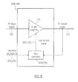
- FIG. 8 shows a block diagram of a further embodiment of an amplifier circuit including a bias controller for receiving frequency information
- FIG. 9 shows a block diagram of an embodiment of a mobile communication device including the embodiment of the amplifier circuit in accordance with FIG. 1 .
- the operating temperature range is typically between ⁇ 10° C. up to 55° C. (according to 3GPP), while the supply voltage ranges typically between 3.0V and 4.3V. The latter is determined by the battery discharge characteristic and voltage drop during transmit operation.
- the radiated power of a mobile terminal strongly depends on the antenna conditions, e.g. free space, talk position (antenna covered by hand or close to head). The different antenna conditions result in different load impedances effective at power amplifier output. In some cases, the power amplifier may need to cope with a wide range of load impedances.
- Antenna mismatch causes, for instance, spectral re-growth issues in transmission schemes with a non-constant envelope such as UMTS and LTE (Long Term Evolution). Both standards have stringent limits for the leakage power on adjacent channels, so-called ACLR (adjacent channel leakage power ratio) requirements.
- ACLR adjacent channel leakage power ratio
- Embodiments of the invention achieve the just-mentioned trade-off by measuring a load impedance of a load coupled to an output of the power amplifier and adjusting a bias control signal of the power amplifier based on the determination of the load impedance measurement. In this way, it is possible to reduce the ACLR degradation under mismatch, so that the ACLR performance can be maintained with comparatively low effort and/or comparatively low current consumption.
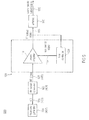
- FIG. 1 shows a block diagram of an embodiment of an amplifier circuit 100 including a bias controller 120 .
- the amplifier circuit 100 comprises a power amplifier 110 and a bias controller 120 .
- the power amplifier 110 is configured to amplify an RF input signal 105 to obtain an RF output signal 115 .
- the bias controller 120 is configured to control a bias of the power amplifier 110 .
- the RF input signal 105 may comprise a plurality of frequencies in specific frequency bands, such as defined by the UMTS standard (or may be switchable between a plurality of frequencies). Referring to the embodiment of FIG.
- the bias controller 120 is configured to determine a measure of a load impedance of a load coupled to an output of the power amplifier 110 and provide a bias control signal 125 for adjusting the bias of the power amplifier 110 based on the determination of the measure of the load impedance.
- a measure of the load impedance is, for example, a quantity that is dependent on the load impedance.
- the RF output signal 115 obtained at the output of the amplifier circuit 100 represents an amplified version of the RF input signal 105 .
- FIG. 2 shows a block diagram of a further embodiment of an amplifier circuit 200 including a bias controller 220 with different look-up tables ( 224 - 1 , 224 - 2 . . . ).
- the amplifier circuit 200 of FIG. 2 essentially comprises the same blocks as the amplifier circuit 100 of FIG. 1 . Therefore, identical blocks having similar implementations and/or functions are denoted by the same numerals.
- the bias controller 220 of the amplifier circuit 200 shown in FIG. 2 may correspond to the bias controller 120 of the amplifier circuit 100 shown in FIG. 1 . Referring to the embodiment of FIG.
- the bias controller 220 may comprise a look-up table 222 configured to store a plurality of bias voltage values associated with corresponding values of a reflection factor for a plurality of load impedances, such that the bias voltage values are dependent on a phase and amplitude (magnitude) of corresponding reflection factors for reflection factors of equal magnitude (e.g. for reflection factors resulting in the same VSWR or Voltage Standing Wave Ratio).
- the bias controller 220 is configured to extract an individual bias voltage value from the look-up table 222 , wherein the individual bias voltage value may correspond to a value of a reflection factor determined by the load impedance.
- the bias controller 220 is configured to provide the bias control signal 125 to adjust the bias of the power amplifier 110 based on the individual bias voltage extracted from the look-up table 222 .
- the bias controller 220 may comprise different look-up tables 224 - 1 , 224 - 2 . . . for a plurality of frequencies of the RF input signal 105 .
- the different look-up tables 224 - 1 , 224 - 2 . . . are denoted by ‘LUT 1 : freq. 1 ’, ‘LUT 2 : freq. 2 ’. . . , indicating that same correspond to different frequencies (freq. 1 , freq. 2 . . . ) of the RF input signal 105 .
- the look-up tables 224 - 1 , 224 - 2 may be considered as sub-tables of the look-up table 222 , as shown in FIG. 2 .
- the look-up tables 224 - 1 , 224 - 2 may alternatively take the place of the look-up table 222 .
- each of the look-up tables (or sub-tables) 224 - 1 , 224 - 2 . . . may be configured to store a plurality of bias voltage values associated with corresponding values of a reflection factor for a plurality of load impedances, such that the bias voltage values are dependent on a phase of corresponding reflection factors for reflection factors of equal magnitude.
- the bias controller 220 may also be configured to extract an individual bias voltage value from a selected look-up table associated with a current frequency of the RF input signal 105 .
- the individual bias voltage value corresponds to a phase of a reflection factor determined by the load impedance for the current frequency of the RF input signal 105 .
- the current frequency of the RF input signal 105 is indicated by the frequency information 205 received by the bias controller 220 comprising the different look-up tables or look-up sub-tables ( 224 - 1 , 224 - 2 . . . ).
- the bias controller 220 is configured to provide the bias control signal 125 to adjust the bias of the power amplifier 110 based on the individual bias voltage value extracted from the selected look-up table.
- FIG. 3 shows a block diagram of a further embodiment of an amplifier circuit 300 including a bias controller 320 with an impedance determinator 322 , a mapping unit 324 and a DCDC converter 326 .
- the amplifier circuit 300 of FIG. 3 essentially comprises the same blocks as the amplifier circuit 100 of FIG. 1 . Therefore, identical blocks having similar implementations and/or functions are denoted by the same numerals.
- the bias controller 320 and a power amplifier supply voltage 325 , Vcc, of the amplifier circuit 300 shown in FIG. 3 corresponds to the bias controller 120 and the bias control signal 125 of the amplifier circuit 100 shown in FIG. 1 . Referring to the embodiment of FIG.
- the amplifier circuit 300 comprises a power amplifier 110 for amplifying an RF input signal 105 based on the power amplifier supply voltage 325 , Vcc, to obtain an RF output signal 115 .
- the bias controller 320 of the amplifier circuit 300 comprises an impedance determinator 322 , a mapping unit 324 and a DCDC converter 326 .
- the impedance determinator 322 is configured to determine a measure 321 , ⁇ L , of a load impedance of a load coupled to an output of the power amplifier 110 , for example in the form of a reflection factor ⁇ L .
- the mapping unit 324 is configured to map the measure 321 of the load impedance to a mapped voltage 323 , Vramp, such that the mapped voltage Vramp is dependent on a phase and amplitude of the reflection factor ⁇ L determined by the load impedance.
- ⁇ L is just a different representation of the load impedance as an S-parameter considering a predetermined reference impedance.
- the DCDC converter 326 is configured to adjust the supply voltage 325 of the power amplifier 110 based on the mapped voltage 323 . In the embodiment of FIG.
- the mapping unit 324 is configured to provide the mapped voltage 323 such that an adjacent channel leakage power ratio (ACLR) value of the RF output signal 115 lies within a predefined range for a plurality of load impedances resulting in reflection factors of equal magnitude and different phase.
- ACLR adjacent channel leakage power ratio
- FIG. 4 shows a block diagram of a further embodiment of an amplifier circuit 400 including a bias controller 420 with an impedance information look-up table 424 (LUT B).
- the amplifier circuit 400 comprises a power amplifier 410 , a bias controller 420 and a directional coupler 406 .
- the power amplifier 410 and the bias controller 420 of the amplifier circuit 400 shown in FIG. 4 may correspond to the power amplifier 110 and the bias controller 120 of the amplifier circuit 100 shown in FIG. 1 .
- a baseband generator 402 baseband generator ‘BB’
- RF signal generator 404 ‘RF signal generation’
- the baseband generator 402 is configured to generate a baseband signal 403 , s(t), while the RF signal generator 404 is configured to generate an RF signal 405 on the basis of the baseband signal 403 , s(t).
- the power amplifier 410 is configured to receive the RF signal 405 from the RF signal generator 404 to obtain an RF output signal 415 .
- the RF signal 405 received by the power amplifier 410 and the RF output signal 415 output by the power amplifier 410 as shown in the embodiment of FIG. 4 correspond to the RF input signal 105 received by the power amplifier 110 and the RF output signal 115 output by the power amplifier 110 as shown in the embodiment of FIG. 1 .
- the power amplifier 410 of FIG. 4 comprises a power amplifier unit 412 connected to an RF front end 414 .
- the directional coupler 406 of the amplifier circuit 400 is coupled to the output of the power amplifier unit 412 or to the output of the RF frontend 414 such that it can be used to perform a reflection factor measurement in dependence on a load impedance.
- the bias controller 420 of the amplifier circuit 400 comprises an impedance determinator 422 , an impedance information look-up table 424 (LUT B), a look-up table 426 (LUT A), a first digital-to-analog converter (DAC) 428 - 1 , a second digital-to-analog converter (DAC) 428 - 2 and a DCDC converter 430 .
- the impedance determinator 422 is denoted by ‘determine antenna impedance ’
- the look-up table 426 of FIG. 4 may correspond to the look-up table 222 of FIG. 2
- the impedance determinator 422 and the DCDC converter 430 of FIG. 4 may correspond to the impedance determinator 322 and the DCDC converter 326 of FIG. 3 .
- the directional coupler 406 is configured to provide a measurement signal 407 representing, for example, a complex load impedance and forward the provided measurement signal 407 to the impedance determinator 422 of the bias controller 420 .
- the impedance determinator 422 may, in turn, be configured to determine a measure 421 , , of the (complex-valued) load impedance, such as a complex-valued reflection factor .
- the measure 421 , , of the load impedance obtained by the impedance determinator 422 as shown in FIG. 4 may correspond to the measure 321 , , of the load impedance obtained by the impedance determinator 322 as shown in FIG. 3 .
- the impedance information look-up table 424 of the bias controller 420 may be configured for storing a plurality of measures of a load impedance for corresponding frequencies of the RF input signal 405 based on the measured impedance information 421 , .
- the bias controller 420 is configured to extract an individual measure 425 of a load impedance from the impedance information look-up table 424 (LUT B).
- the individual measure 425 of the load impedance may correspond to a frequency of the RF input signal 405 such as in a frequency hopping mode.
- the bias controller 420 is configured to provide the bias control signal to adjust the bias of the power amplifier 410 based on the individual measure 425 of the load impedance extracted from the impedance information look-up table 424 . Accordingly, a currently measured impedance value 421 may be used as the impedance measure 425 if the look-up table 424 does not comprise a stored, previously measured impedance value, and a stored, previously measured impedance value from the look-up table 424 may be used as the impedance measure 425 otherwise.
- the bias controller 420 is configured to extract a first and a second digital bias voltage value 427 - 1 , 427 - 2 from the look-up table 426 based on the individual measure 425 of the load impedance extracted from the impedance information look-up table 424 or based on a measured impedance information 421 .
- the first and second digital bias voltage values 427 - 1 , 427 - 2 represent voltages Vcc or Vcq derived from a functional dependence on a measure of the load impedance or the reflection factor, respectively.
- the first and second digital bias voltage values 427 - 1 , 427 - 2 extracted from the look-up table 426 are converted into a first analog bias voltage value 429 - 1 , Vramp, and a second analog bias voltage value 429 - 2 , Vcq, by the first and second digital-to-analog converters 428 - 1 , 428 - 2 , respectively.
- the DCDC converter 430 of the bias controller 420 is configured to adjust the supply voltage 435 , Vcc, of the power amplifier 412 based on the first analog bias voltage value 429 - 1 , Vramp.
- the first analog bias voltage value 429 - 1 and the supply voltage 435 in the embodiment of FIG. 4 essentially correspond to the mapped voltage 323 and the supply voltage 325 in the embodiment of FIG. 3 , respectively.
- the DCDC converter 430 is configured to adjust a supply voltage 435 of the power amplifier 410 based on a mapped voltage 429 - 1 determined by an entry of a look-up table 426 (LUT A).
- the bias controller 420 is configured to provide a first bias control signal to adjust a supply voltage 435 , Vcc, of the power amplifier 410 .
- the bias controller 420 is configured to provide a second bias control signal to adjust an input-sided bias voltage 429 - 2 , Vcq, to adjust a quiescent current of the power amplifier 410 .
- the power amplifier 412 is configured to amplify the RF input signal 405 based on the supply voltage 435 and a quiescent current adjusted by an input-sided bias voltage 429 - 2 (which input-sided bias voltage may, for example, adjust a gate bias or base bias of an amplifier transistor).
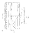
- FIG. 5 shows a graph 500 of an example dependence of an adjacent channel leakage power ratio (ACLR) value 505 on a phase 501 of a reflection factor.
- ACLR adjacent channel leakage power ratio
- the reflection factor may correspond to the reflection factor 321 , 421 obtained from the impedance determinator 322 or 422 in the embodiments of FIG. 3 or 4 , respectively. Since the reflection factor is essentially determined by the load impedance of a load coupled to an output of the power amplifier, the phase 501 of the reflection factor can also be referred to as a “load phase”.
- the adjacent channel leakage power ratio (ACLR) value 505 (in dBc) is typically defined as the ratio of the transmitted power, such as the power in the UMTS transmission channel selected for communication, to the power in the adjacent channel (or as the inverse thereof).
- the ACLR value 505 represents a measure of the power leakage into the adjacent channel, wherein a smaller ACLR value (in dBc) essentially corresponds to a better ACLR performance.
- the battery voltage 506 , Vbatt used for operating the amplifier circuit has an example value of 3.7V.
- the dependencies i.e. ACLR value, supply voltage and battery current
- VSWR Voltage Standing Wave Ratio
- Vmax maximum voltage
- Vmin minimum voltage
- the condition that the VSWR value is constant in the graphs of FIGS. 5-7 means that the corresponding dependencies are associated with a plurality of load impedances resulting in reflection factors of equal magnitude.
- the bias controller of the amplifier circuit is configured to provide a variable supply voltage 435 , 504 denoted by ‘Vcc servoed’ for the power amplifier such that the ACLR value 505 based on the phase 501 of corresponding reflection factors for reflection factors of equal magnitude lies within a predefined range within the total phase angle range 511 .
- Such an ACLR value 505 based on the phase 501 is represented in the graph 500 of FIG. 5 by a second curve 507 - 2 showing a nearly constant behavior over the entire phase angle range.
- the entries of the look-up table 426 may be chosen to adjust the voltage 435 based on the phase of the reflection factor (represented by information 425 ) such that the ACLR is approximately constant (for example, varies by less than ⁇ 2 dB, or even by less than ⁇ 1 dB) over the full phase range from ⁇ 180° to +180°.
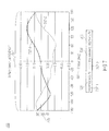
- FIG. 6 shows a graph 600 of an example dependence of a supply voltage 435 , 605 on a phase 501 of a reflection factor (for example, the reflection factor ).
- the Vcc over load phase is shown if Vcc is servoed to obtain a constant ACLR value.
- Vcc servoed
- the supply voltage Vcc may, for example, be provided by the cooperation of the look-up table 426 , the DAC 428 - 1 and the DCDC converter 430 .
- the curve 607 showing the supply voltage 435 , 605 as function of the phase 501 of a reflection factor for a plurality of load impedances resulting in reflection factors of equal magnitude is, for example, characterized by a peak 609 in a first phase angle region 610 for phase angles between ⁇ 70° and ⁇ 50° and a valley 611 in a second phase angle region 620 for phase angles between 60° and 90°.
- a variation ratio of the supply voltage 605 is, for example, less than 1.5:1 over the total phase angle range 511 , wherein the variation ratio can be defined as the ratio of the maximum value 613 and the minimum value 615 of the curve 607 .
- FIG. 7 shows a graph 700 of an example dependence of a battery current 705 on a phase 501 of a reflection factor.
- the graph 700 of FIG. 7 essentially comprises the same components as the graph 500 of FIG. 5 . Therefore, identical components are denoted by the same numerals.
- a first and a second curve 707 - 1 , 707 - 2 representing the current 705 (in A) as a function of the phase 501 (load phase) are depicted within the total phase angle range 511 .
- the first curve 707 - 1 corresponds to a constant supply voltage 502 of 3.7V
- the second curve 707 - 2 corresponds to the variable supply voltage 504 (Vcc servoed).
- the battery voltage 506 for the amplifier circuit is set to an example value of 3.7V. It can clearly be seen in FIG. 7 that in the case of using the variable or servoed supply voltage 504 , the battery current 705 consumed by the power amplifier can be significantly reduced when compared to the case of using the constant supply voltage 502 at least over a significant phase range.
- the second curve 707 - 2 lies at least partially below the first curve 707 - 1 in the graph 700 of FIG. 7 . This is especially the case for phase angles larger than approximately ⁇ 80°.
- the current consumption of the power amplifier can be reduced.
- the load impedance of a load such as an antenna (antenna 408 of FIG. 4 ), coupled to the output of the power amplifier or the antenna impedance can be measured by means of a directional coupler.
- a directional coupler is one implementation, but there are other approaches which can also provide the load impedance.
- a DCDC converter can be used to set the supply voltage Vcc of the power amplifier.
- the DCDC converter can also be realized as a buck-only, boost-only or a buck-boost converter.
- the supply voltage Vcc applied to the power amplifier determines the linear output power capability of the power amplifier.
- a high supply voltage also means a high battery current due to a lower conversion ratio of the DCDC converter.
- the supply voltage is preferably set to a value which should be as low as possible to save battery current, but still high enough to ensure good ACLR performance under all conditions.
- the look-up table (LUT A) can be used to set the bias of the power amplifier depending on the load phase.
- the impedance information look-up table (LUT B) can be used to store the measured load impedances, e.g. depending on transmit channel or frequency information (for example, to be able to rapidly adjust the power amplifier bias in the case of a frequency change).
- FIG. 5 shows the ACLR performance over load phase at VSWR 3:1 load mismatch in two different cases.
- the supply voltage Vcc of the power amplifier is constant at 3.7V and in the second case, the supply voltage Vcc is optimized to keep an example ACLR target of ⁇ 36 dBc over load phase.
- the ACLR performance clearly depends on the load phase angle. This is typical for all linear power amplifiers. Merely the characteristics are different depending on the power amplifier architecture. Single-ended power amplifiers have one maximum over phase as depicted in FIG. 5 . Here, the maximum occurs at ⁇ 120 deg, whereas balanced amplifiers have two maximum values due to the 90 deg hybrid. It can be seen in FIG. 5 that for some phase angles, the ACLR value is much better than needed if Vcc is kept constant. This typical behavior can be used to lower the supply voltage Vcc depending on the phase which means that the Vcc voltage can be reduced at the expense of ACLR headroom. This is also depicted in FIG.
- Vcc servoed means that the power amplifier supply voltage Vcc at each phase angle is adjusted such that the ACLR value will be constant ( ⁇ 36 dBc in this example).
- This adjustment of the supply voltage Vcc can, for example, be achieved by choosing the entries of the look-up table (LUT A) in dependence on the load phase such that the ACLR is approximately constant (for example, varies by less than ⁇ 2 dB, or even by less than ⁇ 1 dB) over the full phase range from ⁇ 180° to +180°.
- FIG. 6 shows the corresponding Vcc response (for example, the Vcc response provided by the cooperation of the look-up table 426 , the DAC 428 - 1 and the DCDC converter 430 in the embodiment of FIG. 4 ) over phase angle.
- the Vcc variation is more than 1V over phase angle.
- Phase angles which correspond to the so-called high impedance range of the power amplifier may, for example, require a high supply voltage preventing the power amplifier from voltage saturation; phase angles which correspond to the low impedance phase range of power amplifier (60 . . . 90 deg) allow a lower supply voltage.
- FIG. 7 shows the impact on the battery current. If Vcc is servoed for constant ACLR in accordance with an embodiment of the invention, the battery current can be greatly reduced, which is a benefit of this invention.
- the battery current can, for example, be reduced by more than 20%, which would result in best class current consumption performance.
- FIG. 8 shows a block diagram of a further embodiment of an amplifier circuit 800 including a bias controller 820 for receiving frequency information 805 .
- the amplifier circuit 800 of FIG. 8 essentially comprises the same blocks as the amplifier circuit 100 of FIG. 1 . Therefore, identical blocks having similar implementations and/or functions are denoted by the same numerals.
- the bias controller 820 of the amplifier circuit 800 is configured to perform the following steps. First, a maximum bias control signal is provided to set the bias of the power amplifier 110 to a maximum level before an initial time slot of a sequence of time slots. Subsequently, the measure of the load impedance is determined. Finally, a bias control signal 825 that is different from the maximum bias control signal is provided to adjust the bias of the power amplifier 110 based on the determination of the measure of the load impedance for a consecutive time slot of the sequence of time slots.
- the bias controller 820 is configured to perform the steps described with regard to the embodiment of FIG. 8 for each frequency of a hopping sequence.
- each of the frequencies of the hopping sequence such as in a frequency hopping mode may be indicated by frequency information 805 received by the bias controller 820 .
- the frequency information 805 received by the bias controller 820 of FIG. 8 may correspond to the frequency information 205 received by the bias controller 220 of FIG. 2 .
- the bias controller 220 or 820 is configured to provide the bias control signal 125 , 825 for the power amplifier 110 based on the frequency information 205 , 805 , respectively.
- the bias controller 820 of the amplifier circuit 800 is configured to store measures of the load impedance for a plurality of frequencies, and to reuse the stored measures of the load impedance when returning to a frequency previously used in the hopping sequence.
- the procedure described above with respect to FIG. 8 may comprise the following steps. First, if the antenna impedance is unknown (e.g. before a first slot or frequency change), the bias of the power amplifier is set to a high level which ensures reasonable ACLR performance independent of the antenna impedance. Then, during a next transmission slot, the antenna impedance is measured. Then, depending on the measured impedance, the bias voltage is set for the next slot.
- the bias control may change the supply voltage and/or the quiescent current of the power amplifier. This is also called dual bias control. In the embodiment described above with regard to FIG. 4 , only (or preferably) the Vcc level is changed. Here, it is pointed out that the dual bias control will further reduce the current consumption, but increase the complexity.
- the just-mentioned procedure steps can be independently applied to each hopping frequency. This can be achieved by a dedicated table (e.g. LUT B in the embodiment of FIG. 4 ) which stores the impedance data for each channel.
- a dedicated table e.g. LUT B in the embodiment of FIG. 4
- the relation between the load impedance and the bias condition is included in the look-up table LUT A.
- This look-up table may, in some cases, be needed for each band which is supported by the mobile device and can be determined by lab measurements. For each band, in some cases, there should be multiple frequency points to compensate the frequency response of the power amplifier. This is especially the case in bands which include a duplexer. It is not necessary to have a table for each output power level. A normalized table relative to the 50 Ohm bias is sufficient.
- the same procedure as described above can be applied to 2G mobile devices to reduce the maximum current under mismatch.
- the reduction of the maximum current is a severe issue due to excessive heat dissipation, especially for Smart Phones.
- the antenna impedance is in the low impedance range of the power amplifier (phase range where the power amplifier draws highest current)
- the output power can be reduced to keep dissipated heat below a certain value.
- the 2G power amplifier was supplied by a DCDC converter, the supply voltage could be lowered to reduce battery current.
- FIG. 9 shows a block diagram of an embodiment of a mobile communication device 900 including the embodiment of the amplifier circuit 100 in accordance with FIG. 1 .
- the mobile communication device 900 for transmitting an RF output signal may comprise a baseband generator 910 , an RF signal generator 920 , a power amplifier 110 , a bias controller 120 and an antenna 930 .
- the power amplifier 110 and the bias controller 120 may constitute the amplifier circuit 100 as shown in the embodiment of FIG. 1 . Therefore, similar blocks in FIG. 9 having similar implementations and/or functions as those in FIG. 1 are denoted by the same numerals.
- the baseband generator 9 may correspond to the baseband generator 402 and the RF signal generator 404 shown in the embodiment of FIG. 4 , while the baseband signal 915 , s(t), and the RF signal 925 obtained from the baseband generator 910 and the RF signal generator 920 may correspond to the baseband signal 403 , s(t), and the RF signal 405 obtained from the baseband generator 402 and the RF signal generator 404 .
- the baseband generator 910 is configured to generate a baseband signal 915 .
- the RF signal generator 920 may be configured for generating an RF signal 925 on the basis of the baseband signal 915 .
- the power amplifier 110 is configured to receive the RF signal 925 from the RF signal generator 920 and for amplifying the received RF signal to obtain an RF output signal 115 .
- the bias controller 120 is configured to control a bias of the power amplifier 110 .
- the bias controller 120 is configured to determine the measure (for example, a reflection factor) of a load impedance of a load coupled to an output of the power amplifier 110 and to provide a bias control signal 125 to adjust the bias of the power amplifier 110 based on the determination of the measure of the load impedance.
- the antenna 930 is configured to transmit the RF output signal 115 as a transmitted RF output signal 935 .
- Some embodiments according to the invention provide a better performance than conventional 3G mobile devices which use an isolator to keep good ACLR performance under antenna mismatch.
- the isolator resolved the linearity degradation under antenna mismatch, but had severe impact on size and cost.
- the increasing number of bands aggravated the cost- and size disadvantage of the isolator approach.
- the isolator was removed from most of the designs and eliminated by other approaches which shall also provide a load-insensitive behavior.
- Today, balanced power amplifiers are the most important class of load-insensitive power amplifier solutions.
- each balanced power amplifier One major disadvantage of each balanced power amplifier is that the load insensitivity is gained at the expense of lower power amplifier efficiency due to additional losses caused by the hybrid network.
- the peak efficiency of a balanced amplifier is typically in the range of 35-37%, whereas a single-ended power amplifier achieves more than 40%.
- Some embodiments according to the invention provide a better tradeoff between efficiency and complexity than amplifiers having more headroom. It has been found that it is often a less effective approach to use a single-ended amplifier with more headroom of linear output power. Due to the extra linear power the ACLR degradation under mismatch is reduced. The advantages compared to a balanced power amplifier are less complex hardware, which allows more cost-effective and smaller size solutions. However, the impact on efficiency is even more severe than in case of a balanced power amplifier if same ALCR performance under mismatch for both architectures is presumed.
- Some embodiments according to the invention provide a better tradeoff between efficiency and complexity than conventional software-based solutions.
- HW hardware
- SW software
- SW software solutions
- aspects have been described in the context of an apparatus, it is clear that these aspects also represent a description of the corresponding method, where a block or device corresponds to a method step or a feature of a method step. Analogously, aspects described in the context of a method step also represent a description of a corresponding block or item or feature of a corresponding apparatus.
- Some or all of the method steps may be executed by (or using) a hardware apparatus, like for example, a microprocessor, a programmable computer or an electronic circuit. In some embodiments, some one or more of the most important method steps may be executed by such an apparatus.
- embodiments of the invention can be implemented in hardware or in software.
- the implementation can be performed using a digital storage medium, for example a floppy disk, a DVD, a Blu-Ray, a CD, a ROM, a PROM, an EPROM, an EEPROM or a FLASH memory, having electronically readable control signals stored thereon, which cooperate (or are capable of cooperating) with a programmable computer system such that the respective method is performed. Therefore, the digital storage medium may be computer readable.
- Some embodiments according to the invention comprise a data carrier having electronically readable control signals, which are capable of cooperating with a programmable computer system, such that one of the methods described herein is performed.
- embodiments of the present invention can be implemented as a computer program product with a program code, the program code being operative for performing one of the methods when the computer program product runs on a computer.
- the program code may for example be stored on a machine readable carrier.
- inventions comprise the computer program for performing one of the methods described herein, stored on a machine readable carrier.
- an embodiment of the inventive method is, therefore, a computer program having a program code for performing one of the methods described herein, when the computer program runs on a computer.
- a further embodiment of the inventive methods is, therefore, a data carrier (or a digital storage medium, or a computer-readable medium) comprising, recorded thereon, the computer program for performing one of the methods described herein.
- the data carrier, the digital storage medium or the recorded medium are typically tangible and/or non-transitionary.
- a further embodiment of the inventive method is, therefore, a data stream or a sequence of signals representing the computer program for performing one of the methods described herein.
- the data stream or the sequence of signals may for example be configured to be transferred via a data communication connection, for example via the Internet.
- a further embodiment comprises a processing means, for example a computer, or a programmable logic device, configured to or adapted to perform one of the methods described herein.
- a processing means for example a computer, or a programmable logic device, configured to or adapted to perform one of the methods described herein.
- a further embodiment comprises a computer having installed thereon the computer program for performing one of the methods described herein.
- a further embodiment according to the invention comprises an apparatus or a system configured to transfer (for example, electronically or optically) a computer program for performing one of the methods described herein to a receiver.
- the receiver may, for example, be a computer, a mobile device, a memory device or the like.
- the apparatus or system may, for example, comprise a file server for transferring the computer program to the receiver.
- a programmable logic device for example a field programmable gate array
- a field programmable gate array may cooperate with a microprocessor in order to perform one of the methods described herein.
- the methods are preferably performed by any hardware apparatus.
- embodiments of the invention offer an attractive solution for a problem which occurs in all mobile terminals based, for example, on 8PSK/GMSK (8-Phase Shift Keying/Gaussian Minimum Shift Keying), WCDMA or LTE.
- Embodiments of the present invention are mostly related to WCDMA, but could also be applied to solve similar problems in other fields.
- Embodiments of the invention provide a procedure which combines a low software complexity with minimum (or, at least, reasonably small) impact on the hardware architecture, thereby allowing for a superior current consumption and ACLR performance under mismatch.
- the knowledge about the antenna impedance or the measurement thereof in a mobile device is important and a prerequisite for embodiments of this invention. Besides this, it is expected that in the future, many mobile devices will support the measurement of the antenna impedance due to other reasons. Such reasons, for example, can be to adjust an antenna tuner or to run a self-test, such as during the production to check whether the antenna is correctly assembled, etc.
- embodiments of the invention have the benefits that a less complex power amplifier can be realized, thereby allowing for a smaller size and cost thereof, and that a higher 50 Ohm peak efficiency can be achieved.
- embodiments of the invention have the benefits that they provide less complex software algorithms, a fast settling time and a feed-forward implementation.
- a fast settling time just one measurement point is needed, while the feed-forward implementation can be made robust, thereby having no stability issues.
- embodiments of the invention provide a concept for setting the bias of a power amplifier depending on the measured load impedance.
- a directional coupler may be used and the ACLR may be kept relatively constant over phase.
- other procedures like pre-distortion could also be employed, requiring a plurality of slots for settling the ACLR value.
Landscapes
- Engineering & Computer Science (AREA)
- Power Engineering (AREA)
- Amplifiers (AREA)
Abstract
Description
- Embodiments of the invention relate to an amplifier circuit, a mobile communication device and a method for adjusting a bias of a power amplifier. Further embodiments of the invention relate to a power amplifier bias optimization based on a measured antenna impedance.
- Conventional methods for adjusting a bias of a power amplifier comprise, for example, methods for reducing a bias current of the power amplifier based on a detected output power level. Such a reduction of the bias current is performed by using a conventional bias control approach. The bias control comprises, for example, a control of a driver for changing the supply voltage of the power amplifier based on certain input parameters. Conventional mobile communication devices including such a bias control are based, for example, on Wideband Code Division Multiple Access (WCDMA). WCDMA describes a multiple access method, while Universal Mobile Telecommunications System (UMTS) is the standard based thereon.
- Embodiments of the invention provide an amplifier circuit, wherein the amplifier circuit comprises a power amplifier for amplifying an RF input signal to obtain an RF output signal and a bias controller for controlling a bias of the power amplifier. The bias controller is configured to determine a measure of a load impedance of a load coupled to an output of the power amplifier and provide a bias control signal for adjusting the bias of the power amplifier based on the determination of the measure of the load impedance.
- Embodiments of the invention provide an amplifier circuit, wherein the amplifier circuit comprises a power amplifier for amplifying an RF input signal based on a supply voltage to obtain an RF output signal, and a bias controller for controlling a bias of the power amplifier. The bias controller comprises an impedance determinator for determining a measure of a load impedance of a load coupled to an output of the power amplifier, and a mapping unit for mapping the measure of the load impedance to a mapped voltage, such that the mapped voltage is dependent on a phase of a reflection factor determined by the load impedance. The bias controller further comprises a DCDC converter configured to adjust the supply voltage of the power amplifier based on the mapped voltage. The mapping unit is configured to provide the mapped voltage such that an adjacent channel leakage power ratio (ACLR) value of the RF output signal lies within a predefined range for a plurality of load impedances resulting in reflection factors of equal magnitude.
- Embodiments of the invention provide an amplifier circuit, wherein the amplifier circuit comprises means for amplifying an RF input signal to obtain an RF output signal and means for controlling a bias of the power amplifier. The means for controlling is configured to determine a measure of a load impedance of a load coupled to an output of the means for amplifying and to provide a bias control signal for adjusting the bias of the means for amplifying based on the determination of the measure of the load impedance.
- Embodiments of the invention provide a mobile communication device for transmitting an RF output signal. The mobile communication device comprises a baseband generator for generating a baseband signal, and an RF signal generator for generating an RF signal based on the baseband signal. The device further comprises a power amplifier for receiving the RF signal from the RF signal generator and amplifying the received RF signal to obtain an RF output signal, and a bias controller for controlling a bias of the power amplifier. The bias controller is configured to determine a measure of a load impedance of a load coupled to an output of the power amplifier and provide a bias control signal for adjusting the bias of the power amplifier based on the determination of the measure of the load impedance. The mobile communication device further comprises an antenna for transmitting the RF output signal.
- Embodiments of the invention provide a method for adjusting a bias of a power amplifier. The method comprises amplifying an RF input signal to obtain an RF output signal, and controlling the bias of the power amplifier. Controlling the bias comprises determining a measure of a load impedance of a load coupled to an output of the power amplifier, and providing a bias control signal for adjusting the bias of the power amplifier based on the determination of the measure of the load impedance.
- Embodiments according to the present invention will subsequently be described in reference to the enclosed Figures in which:
-
FIG. 1 shows a block diagram of an embodiment of an amplifier circuit including a bias controller; -
FIG. 2 shows a block diagram of a further embodiment of an amplifier circuit including a bias controller with different look-up tables; -
FIG. 3 shows a block diagram of a further embodiment of an amplifier circuit including a bias controller with an impedance determinator, a mapping unit and a DCDC converter; -
FIG. 4 shows a block diagram of a further embodiment of an amplifier circuit including a bias controller with an impedance information look-up table; -
FIG. 5 shows a graph of an example dependence of an adjacent channel leakage power ratio (ACLR) value on a phase of a reflection factor; -
FIG. 6 shows a graph of an example dependence of a supply voltage on a phase of a reflection factor; -
FIG. 7 shows a graph of an example dependence of a battery current on a phase of a reflection factor; -
FIG. 8 shows a block diagram of a further embodiment of an amplifier circuit including a bias controller for receiving frequency information; and -
FIG. 9 shows a block diagram of an embodiment of a mobile communication device including the embodiment of the amplifier circuit in accordance withFIG. 1 . - In the following, operation conditions and requirements of some mobile communication devices, in which the present invention may be used, will be described. Some embodiments according to the invention provide good performance under the condition discussed in the following.
- Mobile terminals often have to cope with changing environmental conditions. The operating temperature range is typically between −10° C. up to 55° C. (according to 3GPP), while the supply voltage ranges typically between 3.0V and 4.3V. The latter is determined by the battery discharge characteristic and voltage drop during transmit operation. In addition, the radiated power of a mobile terminal strongly depends on the antenna conditions, e.g. free space, talk position (antenna covered by hand or close to head). The different antenna conditions result in different load impedances effective at power amplifier output. In some cases, the power amplifier may need to cope with a wide range of load impedances. Antenna mismatch causes, for instance, spectral re-growth issues in transmission schemes with a non-constant envelope such as UMTS and LTE (Long Term Evolution). Both standards have stringent limits for the leakage power on adjacent channels, so-called ACLR (adjacent channel leakage power ratio) requirements.
- Therefore, a need exists for an approach of adjusting a bias of a power amplifier allowing to achieve a good trade-off between an improved ACLR performance, a low current consumption and the computational complexity.
- Embodiments of the invention achieve the just-mentioned trade-off by measuring a load impedance of a load coupled to an output of the power amplifier and adjusting a bias control signal of the power amplifier based on the determination of the load impedance measurement. In this way, it is possible to reduce the ACLR degradation under mismatch, so that the ACLR performance can be maintained with comparatively low effort and/or comparatively low current consumption.
-
FIG. 1 shows a block diagram of an embodiment of anamplifier circuit 100 including abias controller 120. As shown inFIG. 1 , theamplifier circuit 100 comprises apower amplifier 110 and abias controller 120. Here, thepower amplifier 110 is configured to amplify anRF input signal 105 to obtain anRF output signal 115. Moreover, thebias controller 120 is configured to control a bias of thepower amplifier 110. TheRF input signal 105 may comprise a plurality of frequencies in specific frequency bands, such as defined by the UMTS standard (or may be switchable between a plurality of frequencies). Referring to the embodiment ofFIG. 1 , thebias controller 120 is configured to determine a measure of a load impedance of a load coupled to an output of thepower amplifier 110 and provide abias control signal 125 for adjusting the bias of thepower amplifier 110 based on the determination of the measure of the load impedance. Such a measure of the load impedance is, for example, a quantity that is dependent on the load impedance. TheRF output signal 115 obtained at the output of theamplifier circuit 100 represents an amplified version of theRF input signal 105. -
FIG. 2 shows a block diagram of a further embodiment of anamplifier circuit 200 including abias controller 220 with different look-up tables (224-1, 224-2 . . . ). Here, theamplifier circuit 200 ofFIG. 2 essentially comprises the same blocks as theamplifier circuit 100 ofFIG. 1 . Therefore, identical blocks having similar implementations and/or functions are denoted by the same numerals. Moreover, thebias controller 220 of theamplifier circuit 200 shown inFIG. 2 may correspond to thebias controller 120 of theamplifier circuit 100 shown inFIG. 1 . Referring to the embodiment ofFIG. 2 , thebias controller 220 may comprise a look-up table 222 configured to store a plurality of bias voltage values associated with corresponding values of a reflection factor for a plurality of load impedances, such that the bias voltage values are dependent on a phase and amplitude (magnitude) of corresponding reflection factors for reflection factors of equal magnitude (e.g. for reflection factors resulting in the same VSWR or Voltage Standing Wave Ratio). Thebias controller 220 is configured to extract an individual bias voltage value from the look-up table 222, wherein the individual bias voltage value may correspond to a value of a reflection factor determined by the load impedance. Here, thebias controller 220 is configured to provide thebias control signal 125 to adjust the bias of thepower amplifier 110 based on the individual bias voltage extracted from the look-up table 222. - It is also shown in
FIG. 2 that thebias controller 220 may comprise different look-up tables 224-1, 224-2 . . . for a plurality of frequencies of theRF input signal 105. Here, the different look-up tables 224-1, 224-2 . . . are denoted by ‘LUT1: freq. 1’, ‘LUT2: freq. 2’. . . , indicating that same correspond to different frequencies (freq. 1, freq. 2 . . . ) of theRF input signal 105. The look-up tables 224-1, 224-2 may be considered as sub-tables of the look-up table 222, as shown inFIG. 2 . However, the look-up tables 224-1, 224-2 may alternatively take the place of the look-up table 222. Referring to the embodiment ofFIG. 2 , each of the look-up tables (or sub-tables) 224-1, 224-2 . . . may be configured to store a plurality of bias voltage values associated with corresponding values of a reflection factor for a plurality of load impedances, such that the bias voltage values are dependent on a phase of corresponding reflection factors for reflection factors of equal magnitude. - Additionally, the
bias controller 220 may also be configured to extract an individual bias voltage value from a selected look-up table associated with a current frequency of theRF input signal 105. In one embodiment the individual bias voltage value corresponds to a phase of a reflection factor determined by the load impedance for the current frequency of theRF input signal 105. It is pointed out that in one embodiment the current frequency of theRF input signal 105 is indicated by thefrequency information 205 received by thebias controller 220 comprising the different look-up tables or look-up sub-tables (224-1, 224-2 . . . ). In the embodiment ofFIG. 2 , thebias controller 220 is configured to provide thebias control signal 125 to adjust the bias of thepower amplifier 110 based on the individual bias voltage value extracted from the selected look-up table. -
FIG. 3 shows a block diagram of a further embodiment of anamplifier circuit 300 including abias controller 320 with animpedance determinator 322, amapping unit 324 and aDCDC converter 326. Here, theamplifier circuit 300 ofFIG. 3 essentially comprises the same blocks as theamplifier circuit 100 ofFIG. 1 . Therefore, identical blocks having similar implementations and/or functions are denoted by the same numerals. Moreover, thebias controller 320 and a poweramplifier supply voltage 325, Vcc, of theamplifier circuit 300 shown inFIG. 3 corresponds to thebias controller 120 and thebias control signal 125 of theamplifier circuit 100 shown inFIG. 1 . Referring to the embodiment ofFIG. 3 , theamplifier circuit 300 comprises apower amplifier 110 for amplifying anRF input signal 105 based on the poweramplifier supply voltage 325, Vcc, to obtain anRF output signal 115. It can also be seen inFIG. 3 that thebias controller 320 of theamplifier circuit 300 comprises animpedance determinator 322, amapping unit 324 and aDCDC converter 326. Here, theimpedance determinator 322 is configured to determine ameasure 321, □L, of a load impedance of a load coupled to an output of thepower amplifier 110, for example in the form of a reflection factor □L. Themapping unit 324 is configured to map themeasure 321 of the load impedance to a mappedvoltage 323, Vramp, such that the mapped voltage Vramp is dependent on a phase and amplitude of the reflection factor □L determined by the load impedance. Here, □L is just a different representation of the load impedance as an S-parameter considering a predetermined reference impedance. TheDCDC converter 326 is configured to adjust thesupply voltage 325 of thepower amplifier 110 based on the mappedvoltage 323. In the embodiment ofFIG. 3 , themapping unit 324 is configured to provide the mappedvoltage 323 such that an adjacent channel leakage power ratio (ACLR) value of theRF output signal 115 lies within a predefined range for a plurality of load impedances resulting in reflection factors of equal magnitude and different phase. -
FIG. 4 shows a block diagram of a further embodiment of anamplifier circuit 400 including abias controller 420 with an impedance information look-up table 424 (LUT B). As shown inFIG. 4 , theamplifier circuit 400 comprises apower amplifier 410, abias controller 420 and adirectional coupler 406. Here, thepower amplifier 410 and thebias controller 420 of theamplifier circuit 400 shown inFIG. 4 may correspond to thepower amplifier 110 and thebias controller 120 of theamplifier circuit 100 shown inFIG. 1 . In the embodiment ofFIG. 4 , a baseband generator 402 (baseband generator ‘BB’) and an RF signal generator 404 (‘RF signal generation’) are also shown. In particular, thebaseband generator 402 is configured to generate abaseband signal 403, s(t), while theRF signal generator 404 is configured to generate anRF signal 405 on the basis of thebaseband signal 403, s(t). It can also be seen inFIG. 4 that thepower amplifier 410 is configured to receive the RF signal 405 from theRF signal generator 404 to obtain anRF output signal 415. Here, the RF signal 405 received by thepower amplifier 410 and theRF output signal 415 output by thepower amplifier 410 as shown in the embodiment ofFIG. 4 correspond to theRF input signal 105 received by thepower amplifier 110 and theRF output signal 115 output by thepower amplifier 110 as shown in the embodiment ofFIG. 1 . Moreover, thepower amplifier 410 ofFIG. 4 comprises apower amplifier unit 412 connected to an RFfront end 414. - The
directional coupler 406 of theamplifier circuit 400 is coupled to the output of thepower amplifier unit 412 or to the output of theRF frontend 414 such that it can be used to perform a reflection factor measurement in dependence on a load impedance. - Referring to the embodiment of
FIG. 4 , thebias controller 420 of theamplifier circuit 400 comprises animpedance determinator 422, an impedance information look-up table 424 (LUT B), a look-up table 426 (LUT A), a first digital-to-analog converter (DAC) 428-1, a second digital-to-analog converter (DAC) 428-2 and aDCDC converter 430. Here, theimpedance determinator 422 is denoted by ‘determine antenna impedance’, while the impedance information look-up table 424 and the look-up table 426 are denoted by ‘LUT B: store data’ and ‘LUT A: Vcq=f(); Vcc=f()’, respectively. Moreover, the look-up table 426 of
FIG. 4 may correspond to the look-up table 222 ofFIG. 2 , while theimpedance determinator 422 and theDCDC converter 430 ofFIG. 4 may correspond to theimpedance determinator 322 and theDCDC converter 326 ofFIG. 3 . - According to the embodiment of
FIG. 4 , the directional coupler 406 is configured to provide a measurement signal 407 representing, for example, a complex load impedance and forward the provided measurement signal 407 to the impedance determinator 422 of the bias controller 420. The impedance determinator 422 may, in turn, be configured to determine a measure 421,, of the (complex-valued) load impedance, such as a complex-valued reflection factor. Here, the measure 421,, of the load impedance obtained by the impedance determinator 422 as shown inFIG. 4 may correspond to the measure 321,, of the load impedance obtained by theimpedance determinator 322 as shown inFIG. 3 . - In the embodiment of
FIG. 4 , the impedance information look-up table 424 of the bias controller 420 may be configured for storing a plurality of measures of a load impedance for corresponding frequencies of the RF input signal 405 based on the measured impedance information 421,. In addition, thebias controller 420 is configured to extract anindividual measure 425 of a load impedance from the impedance information look-up table 424 (LUT B). Here, theindividual measure 425 of the load impedance may correspond to a frequency of theRF input signal 405 such as in a frequency hopping mode. Moreover, thebias controller 420 is configured to provide the bias control signal to adjust the bias of thepower amplifier 410 based on theindividual measure 425 of the load impedance extracted from the impedance information look-up table 424. Accordingly, a currently measuredimpedance value 421 may be used as theimpedance measure 425 if the look-up table 424 does not comprise a stored, previously measured impedance value, and a stored, previously measured impedance value from the look-up table 424 may be used as theimpedance measure 425 otherwise. - As depicted in the embodiment of
FIG. 4 , thebias controller 420 is configured to extract a first and a second digital bias voltage value 427-1, 427-2 from the look-up table 426 based on theindividual measure 425 of the load impedance extracted from the impedance information look-up table 424 or based on a measuredimpedance information 421. In one embodiment the first and second digital bias voltage values 427-1, 427-2 represent voltages Vcc or Vcq derived from a functional dependence on a measure of the load impedance or the reflection factor, respectively. - The first and second digital bias voltage values 427-1, 427-2 extracted from the look-up table 426 are converted into a first analog bias voltage value 429-1, Vramp, and a second analog bias voltage value 429-2, Vcq, by the first and second digital-to-analog converters 428-1, 428-2, respectively. The
DCDC converter 430 of thebias controller 420 is configured to adjust thesupply voltage 435, Vcc, of thepower amplifier 412 based on the first analog bias voltage value 429-1, Vramp. Here, the first analog bias voltage value 429-1 and thesupply voltage 435 in the embodiment ofFIG. 4 essentially correspond to the mappedvoltage 323 and thesupply voltage 325 in the embodiment ofFIG. 3 , respectively. - In other words, the
DCDC converter 430 is configured to adjust asupply voltage 435 of thepower amplifier 410 based on a mapped voltage 429-1 determined by an entry of a look-up table 426 (LUT A). - Therefore, as shown in
FIG. 4 , in one embodiment thebias controller 420 is configured to provide a first bias control signal to adjust asupply voltage 435, Vcc, of thepower amplifier 410. In addition, thebias controller 420 is configured to provide a second bias control signal to adjust an input-sided bias voltage 429-2, Vcq, to adjust a quiescent current of thepower amplifier 410. - Specifically, in the embodiment of
FIG. 4 , thepower amplifier 412 is configured to amplify theRF input signal 405 based on thesupply voltage 435 and a quiescent current adjusted by an input-sided bias voltage 429-2 (which input-sided bias voltage may, for example, adjust a gate bias or base bias of an amplifier transistor). -
FIG. 5 shows agraph 500 of an example dependence of an adjacent channel leakage power ratio (ACLR)value 505 on aphase 501 of a reflection factor. Specifically, inFIG. 5 , the ACLR over load phase for Vcc=constant=3.7V and ‘Vcc servoed’ is shown. Here, the reflection factor may correspond to thereflection factor impedance determinator FIG. 3 or 4, respectively. Since the reflection factor is essentially determined by the load impedance of a load coupled to an output of the power amplifier, thephase 501 of the reflection factor can also be referred to as a “load phase”. The adjacent channel leakage power ratio (ACLR) value 505 (in dBc) is typically defined as the ratio of the transmitted power, such as the power in the UMTS transmission channel selected for communication, to the power in the adjacent channel (or as the inverse thereof). Thus, theACLR value 505 represents a measure of the power leakage into the adjacent channel, wherein a smaller ACLR value (in dBc) essentially corresponds to a better ACLR performance. - According to embodiments of the invention, the power amplifier may be configured as, for example, a single-ended power amplifier such that, for a constant supply voltage 502 (e.g. Vcc=3.7V) of the power amplifier, a dependence of the
ACLR value 505 of the RF output signal on the phase 501 (in deg or degrees) of a reflection factor for a plurality of load impedances resulting in reflection factors of equal magnitude (i.e. for a given VSWR), such as represented by a first curve 507-1 in thegraph 500 ofFIG. 5 , comprises, for example, asingle peak 509 within a totalphase angle range 511 between −180 and 180°. Here, it is to be noted that in thegraph 500 ofFIG. 5 , thebattery voltage 506, Vbatt, used for operating the amplifier circuit has an example value of 3.7V. - It is also pointed out here that in the
graphs FIGS. 5 , 6 and 7, the dependencies (i.e. ACLR value, supply voltage and battery current) are specifically shown for an example Voltage Standing Wave Ratio (VSWR) value of 3:1. The Voltage Standing Wave Ratio is typically defined as the ratio of a maximum voltage (Vmax) and a minimum voltage (Vmin) of a standing wave and depends on the magnitude of the reflection factor () determined by the load impedance, as it is well known to one skilled in the art. Here, the maximum voltage Vmax essentially corresponds to the sum of the voltage VF of a forward propagating wave at the output of the power amplifier and the voltage VR of a reflected wave reflected by the load impedance of a load coupled to the output of the power amplifier (i.e. Vmax=VF+VR), while the minimum voltage Vmin essentially corresponds to the difference between the voltage VF of the forward propagating wave and the voltage VR of the reflected wave (i.e. Vmin=VF−VR): - The condition that the VSWR value is constant in the graphs of
FIGS. 5-7 means that the corresponding dependencies are associated with a plurality of load impedances resulting in reflection factors of equal magnitude. - In embodiments related to
FIG. 5 , the bias controller of the amplifier circuit is configured to provide avariable supply voltage ACLR value 505 based on thephase 501 of corresponding reflection factors for reflection factors of equal magnitude lies within a predefined range within the totalphase angle range 511. Such anACLR value 505 based on thephase 501 is represented in thegraph 500 ofFIG. 5 by a second curve 507-2 showing a nearly constant behavior over the entire phase angle range. In particular, the second curve 507-2 of thegraph 500 ofFIG. 5 may have ACLR values lying, for example, in the predefined range between −37 and −35 dBc, while preferably, thevariable supply voltage voltage 435 based on the phase of the reflection factor(represented by information 425) such that the ACLR is approximately constant (for example, varies by less than ±2 dB, or even by less than ±1 dB) over the full phase range from −180° to +180°. -
FIG. 6 shows agraph 600 of an example dependence of asupply voltage phase 501 of a reflection factor (for example, the reflection factor). Specifically, inFIG. 6 , the Vcc over load phase is shown if Vcc is servoed to obtain a constant ACLR value. In thegraph 600 ofFIG. 6 , acurve 607 is shown representing thesupply voltage phase 501 of corresponding reflection factors (for example, the reflection factor) for reflection factors of equal magnitude (VSWR=3:1) over the totalphase angle range 511. Here, thesupply voltage 605 depicted in thegraph 600 ofFIG. 6 may correspond to thesupply voltage 435, 504 (Vcc servoed) provided for the power amplifier as described with regard toFIG. 5 . The supply voltage Vcc, as shown inFIG. 6 , may, for example, be provided by the cooperation of the look-up table 426, the DAC 428-1 and theDCDC converter 430. - It can be seen in the
graph 600 ofFIG. 6 that thecurve 607 showing thesupply voltage phase 501 of a reflection factor for a plurality of load impedances resulting in reflection factors of equal magnitude is, for example, characterized by apeak 609 in a first phase angle region 610 for phase angles between −70° and −50° and avalley 611 in a second phase angle region 620 for phase angles between 60° and 90°. - In embodiments referring to
FIG. 6 , a variation ratio of thesupply voltage 605 is, for example, less than 1.5:1 over the totalphase angle range 511, wherein the variation ratio can be defined as the ratio of themaximum value 613 and theminimum value 615 of thecurve 607. -
FIG. 7 shows agraph 700 of an example dependence of a battery current 705 on aphase 501 of a reflection factor. Specifically, inFIG. 7 , the battery current over load phase for Vcc=constant=3.7V and Vcc servoed' is shown. Thegraph 700 ofFIG. 7 essentially comprises the same components as thegraph 500 ofFIG. 5 . Therefore, identical components are denoted by the same numerals. In thegraph 700 ofFIG. 7 , a first and a second curve 707-1, 707-2 representing the current 705 (in A) as a function of the phase 501 (load phase) are depicted within the totalphase angle range 511. Here, thephase 501 of thegraph 700 shown inFIG. 7 corresponds to reflection factors for reflection factors of equal magnitude as in thegraph FIGS. 5 and 6 (VSWR=3:1). In addition, the first curve 707-1 corresponds to aconstant supply voltage 502 of 3.7V, while the second curve 707-2 corresponds to the variable supply voltage 504 (Vcc servoed). Thebattery voltage 506 for the amplifier circuit is set to an example value of 3.7V. It can clearly be seen inFIG. 7 that in the case of using the variable orservoed supply voltage 504, the battery current 705 consumed by the power amplifier can be significantly reduced when compared to the case of using theconstant supply voltage 502 at least over a significant phase range. Correspondingly, the second curve 707-2 lies at least partially below the first curve 707-1 in thegraph 700 ofFIG. 7 . This is especially the case for phase angles larger than approximately −80°. Thus, by adjusting the supply voltage of the power amplifier based on the load phase, to obtain an ACLR value of the RF output signal which lies within a predefined range, the current consumption of the power amplifier can be reduced. - To recap the embodiment described with regard to
FIG. 4 , the load impedance of a load, such as an antenna (antenna 408 ofFIG. 4 ), coupled to the output of the power amplifier or the antenna impedance can be measured by means of a directional coupler. However, each method which provides phase and magnitude of the antenna impedance can be applicable for embodiments of the invention. The use of a directional coupler is one implementation, but there are other approaches which can also provide the load impedance. A DCDC converter can be used to set the supply voltage Vcc of the power amplifier. According to further embodiments of the present invention, the DCDC converter can also be realized as a buck-only, boost-only or a buck-boost converter. The supply voltage Vcc applied to the power amplifier determines the linear output power capability of the power amplifier. The higher the supply voltage is, the higher is the maximum linear output power of the power amplifier. However, a high supply voltage also means a high battery current due to a lower conversion ratio of the DCDC converter. Thus, the supply voltage is preferably set to a value which should be as low as possible to save battery current, but still high enough to ensure good ACLR performance under all conditions. The look-up table (LUT A) can be used to set the bias of the power amplifier depending on the load phase. The impedance information look-up table (LUT B) can be used to store the measured load impedances, e.g. depending on transmit channel or frequency information (for example, to be able to rapidly adjust the power amplifier bias in the case of a frequency change). - The basic concept of the invention will be summarized in the following.
FIG. 5 shows the ACLR performance over load phase at VSWR 3:1 load mismatch in two different cases. In the first case, the supply voltage Vcc of the power amplifier is constant at 3.7V and in the second case, the supply voltage Vcc is optimized to keep an example ACLR target of −36 dBc over load phase. - If the supply voltage Vcc is constant at 3.7V or any other value inside battery voltage range, the ACLR performance clearly depends on the load phase angle. This is typical for all linear power amplifiers. Merely the characteristics are different depending on the power amplifier architecture. Single-ended power amplifiers have one maximum over phase as depicted in
FIG. 5 . Here, the maximum occurs at −120 deg, whereas balanced amplifiers have two maximum values due to the 90deg hybrid. It can be seen inFIG. 5 that for some phase angles, the ACLR value is much better than needed if Vcc is kept constant. This typical behavior can be used to lower the supply voltage Vcc depending on the phase which means that the Vcc voltage can be reduced at the expense of ACLR headroom. This is also depicted inFIG. 5 as case “Vcc servoed”. Here “Vcc servoed” means that the power amplifier supply voltage Vcc at each phase angle is adjusted such that the ACLR value will be constant (−36 dBc in this example). This adjustment of the supply voltage Vcc can, for example, be achieved by choosing the entries of the look-up table (LUT A) in dependence on the load phase such that the ACLR is approximately constant (for example, varies by less than ±2 dB, or even by less than ±1 dB) over the full phase range from −180° to +180°. -
FIG. 6 shows the corresponding Vcc response (for example, the Vcc response provided by the cooperation of the look-up table 426, the DAC 428-1 and theDCDC converter 430 in the embodiment ofFIG. 4 ) over phase angle. The Vcc variation is more than 1V over phase angle. Phase angles which correspond to the so-called high impedance range of the power amplifier (−60 deg in this example) may, for example, require a high supply voltage preventing the power amplifier from voltage saturation; phase angles which correspond to the low impedance phase range of power amplifier (60 . . . 90 deg) allow a lower supply voltage. -
FIG. 7 shows the impact on the battery current. If Vcc is servoed for constant ACLR in accordance with an embodiment of the invention, the battery current can be greatly reduced, which is a benefit of this invention. - The proper Vcc setting may require knowledge about the load impedance. If the load impedance is known, the Vcc voltage can be set to the lowest possible value, which is high enough to maintain a certain target ACLR performance as shown in
FIG. 6 . This method also significantly reduces the 50 Ohm current which is important for benchmarking. In case of Vcc=constant, the battery current of 50 Ohm is roughly 370 mA for this power amplifier type. In case of “Vcc servoed” to an ACLR target of −36 dBc, the battery current is 297 mA at Vbatt=3.7V. The required Vcc to achieve an ACLR value of −36 dBc at 50 Ohm is, for example, 2.8V. If the battery voltage is 3.7V, the conversion ratio is 3.7V/2.8V=1.32. Assuming a DCDC converter efficiency of 93%, the current is reduced by a factor 1.32*0.93=1.23. By removing the power headroom which is not needed at 50 Ohm, the battery current can, for example, be reduced by more than 20%, which would result in best class current consumption performance. -
FIG. 8 shows a block diagram of a further embodiment of anamplifier circuit 800 including abias controller 820 for receivingfrequency information 805. Theamplifier circuit 800 ofFIG. 8 essentially comprises the same blocks as theamplifier circuit 100 ofFIG. 1 . Therefore, identical blocks having similar implementations and/or functions are denoted by the same numerals. However, in the embodiment ofFIG. 8 , thebias controller 820 of theamplifier circuit 800 is configured to perform the following steps. First, a maximum bias control signal is provided to set the bias of thepower amplifier 110 to a maximum level before an initial time slot of a sequence of time slots. Subsequently, the measureof the load impedance is determined. Finally, abias control signal 825 that is different from the maximum bias control signal is provided to adjust the bias of thepower amplifier 110 based on the determination of the measureof the load impedance for a consecutive time slot of the sequence of time slots. - For example, the
bias controller 820 is configured to perform the steps described with regard to the embodiment ofFIG. 8 for each frequency of a hopping sequence. Here, each of the frequencies of the hopping sequence such as in a frequency hopping mode may be indicated byfrequency information 805 received by thebias controller 820. Thefrequency information 805 received by thebias controller 820 ofFIG. 8 may correspond to thefrequency information 205 received by thebias controller 220 ofFIG. 2 . Thus, in the embodiments ofFIGS. 2 and 8 , thebias controller bias control signal power amplifier 110 based on thefrequency information - According to the embodiment of
FIG. 8 , thebias controller 820 of theamplifier circuit 800 is configured to store measures of the load impedance for a plurality of frequencies, and to reuse the stored measures of the load impedance when returning to a frequency previously used in the hopping sequence. - In accordance with further embodiments, the procedure described above with respect to
FIG. 8 may comprise the following steps. First, if the antenna impedance is unknown (e.g. before a first slot or frequency change), the bias of the power amplifier is set to a high level which ensures reasonable ACLR performance independent of the antenna impedance. Then, during a next transmission slot, the antenna impedance is measured. Then, depending on the measured impedance, the bias voltage is set for the next slot. In embodiments, the bias control may change the supply voltage and/or the quiescent current of the power amplifier. This is also called dual bias control. In the embodiment described above with regard toFIG. 4 , only (or preferably) the Vcc level is changed. Here, it is pointed out that the dual bias control will further reduce the current consumption, but increase the complexity. - Additionally, if the mobile device operates in a frequency hopping mode, the just-mentioned procedure steps can be independently applied to each hopping frequency. This can be achieved by a dedicated table (e.g. LUT B in the embodiment of
FIG. 4 ) which stores the impedance data for each channel. - Again referring to the embodiment of
FIG. 4 , the relation between the load impedance and the bias condition is included in the look-up table LUT A. This look-up table may, in some cases, be needed for each band which is supported by the mobile device and can be determined by lab measurements. For each band, in some cases, there should be multiple frequency points to compensate the frequency response of the power amplifier. This is especially the case in bands which include a duplexer. It is not necessary to have a table for each output power level. A normalized table relative to the 50 Ohm bias is sufficient. - In a further embodiment, the same procedure as described above can be applied to 2G mobile devices to reduce the maximum current under mismatch. The reduction of the maximum current is a severe issue due to excessive heat dissipation, especially for Smart Phones. If the antenna impedance is in the low impedance range of the power amplifier (phase range where the power amplifier draws highest current), the output power can be reduced to keep dissipated heat below a certain value. If the 2G power amplifier was supplied by a DCDC converter, the supply voltage could be lowered to reduce battery current. By evaluating the load impedance, the heat dissipation can be easily limited which is important for the phone suppliers.
-
FIG. 9 shows a block diagram of an embodiment of amobile communication device 900 including the embodiment of theamplifier circuit 100 in accordance withFIG. 1 . As shown inFIG. 9 , themobile communication device 900 for transmitting an RF output signal may comprise abaseband generator 910, anRF signal generator 920, apower amplifier 110, abias controller 120 and anantenna 930. Here, thepower amplifier 110 and thebias controller 120 may constitute theamplifier circuit 100 as shown in the embodiment ofFIG. 1 . Therefore, similar blocks inFIG. 9 having similar implementations and/or functions as those inFIG. 1 are denoted by the same numerals. Moreover, thebaseband generator 910 and theRF signal generator 920 of themobile communication device 900 shown inFIG. 9 may correspond to thebaseband generator 402 and theRF signal generator 404 shown in the embodiment ofFIG. 4 , while thebaseband signal 915, s(t), and the RF signal 925 obtained from thebaseband generator 910 and theRF signal generator 920 may correspond to thebaseband signal 403, s(t), and the RF signal 405 obtained from thebaseband generator 402 and theRF signal generator 404. In the embodiment ofFIG. 9 , thebaseband generator 910 is configured to generate abaseband signal 915. TheRF signal generator 920 may be configured for generating anRF signal 925 on the basis of thebaseband signal 915. Thepower amplifier 110 is configured to receive the RF signal 925 from theRF signal generator 920 and for amplifying the received RF signal to obtain anRF output signal 115. Thebias controller 120 is configured to control a bias of thepower amplifier 110. Here, thebias controller 120 is configured to determine the measure(for example, a reflection factor) of a load impedance of a load coupled to an output of thepower amplifier 110 and to provide abias control signal 125 to adjust the bias of thepower amplifier 110 based on the determination of the measureof the load impedance. Theantenna 930 is configured to transmit theRF output signal 115 as a transmittedRF output signal 935. - Some embodiments according to the invention provide a better performance than conventional 3G mobile devices which use an isolator to keep good ACLR performance under antenna mismatch. The isolator resolved the linearity degradation under antenna mismatch, but had severe impact on size and cost. The increasing number of bands aggravated the cost- and size disadvantage of the isolator approach. As a result, the isolator was removed from most of the designs and eliminated by other approaches which shall also provide a load-insensitive behavior. Today, balanced power amplifiers are the most important class of load-insensitive power amplifier solutions. There are some design variants depending on the power amplifier supplier, but all implementations rely on a 90deg hybrid as a core element to reduce the load sensitivity. One major disadvantage of each balanced power amplifier is that the load insensitivity is gained at the expense of lower power amplifier efficiency due to additional losses caused by the hybrid network. The peak efficiency of a balanced amplifier is typically in the range of 35-37%, whereas a single-ended power amplifier achieves more than 40%.
- Some embodiments according to the invention provide a better tradeoff between efficiency and complexity than amplifiers having more headroom. It has been found that it is often a less effective approach to use a single-ended amplifier with more headroom of linear output power. Due to the extra linear power the ACLR degradation under mismatch is reduced. The advantages compared to a balanced power amplifier are less complex hardware, which allows more cost-effective and smaller size solutions. However, the impact on efficiency is even more severe than in case of a balanced power amplifier if same ALCR performance under mismatch for both architectures is presumed.
- Some embodiments according to the invention provide a better tradeoff between efficiency and complexity than conventional software-based solutions. Apart from the hardware (HW) based solutions described above there are some software (SW) solutions, which are also aimed to improve ACLR under mismatch and which have less impact on efficiency, cost or power amplifier complexity. Good examples are pre-distortion and adaptive biasing. The disadvantage here is a significantly higher software complexity which, so far, impedes deployment in mobile devices.
- Although some aspects have been described in the context of an apparatus, it is clear that these aspects also represent a description of the corresponding method, where a block or device corresponds to a method step or a feature of a method step. Analogously, aspects described in the context of a method step also represent a description of a corresponding block or item or feature of a corresponding apparatus. Some or all of the method steps may be executed by (or using) a hardware apparatus, like for example, a microprocessor, a programmable computer or an electronic circuit. In some embodiments, some one or more of the most important method steps may be executed by such an apparatus.
- Depending on certain implementation requirements, embodiments of the invention can be implemented in hardware or in software. The implementation can be performed using a digital storage medium, for example a floppy disk, a DVD, a Blu-Ray, a CD, a ROM, a PROM, an EPROM, an EEPROM or a FLASH memory, having electronically readable control signals stored thereon, which cooperate (or are capable of cooperating) with a programmable computer system such that the respective method is performed. Therefore, the digital storage medium may be computer readable.
- Some embodiments according to the invention comprise a data carrier having electronically readable control signals, which are capable of cooperating with a programmable computer system, such that one of the methods described herein is performed.
- Generally, embodiments of the present invention can be implemented as a computer program product with a program code, the program code being operative for performing one of the methods when the computer program product runs on a computer. The program code may for example be stored on a machine readable carrier.
- Other embodiments comprise the computer program for performing one of the methods described herein, stored on a machine readable carrier.
- In other words, an embodiment of the inventive method is, therefore, a computer program having a program code for performing one of the methods described herein, when the computer program runs on a computer.
- A further embodiment of the inventive methods is, therefore, a data carrier (or a digital storage medium, or a computer-readable medium) comprising, recorded thereon, the computer program for performing one of the methods described herein. The data carrier, the digital storage medium or the recorded medium are typically tangible and/or non-transitionary.
- A further embodiment of the inventive method is, therefore, a data stream or a sequence of signals representing the computer program for performing one of the methods described herein. The data stream or the sequence of signals may for example be configured to be transferred via a data communication connection, for example via the Internet.
- A further embodiment comprises a processing means, for example a computer, or a programmable logic device, configured to or adapted to perform one of the methods described herein.
- A further embodiment comprises a computer having installed thereon the computer program for performing one of the methods described herein.
- A further embodiment according to the invention comprises an apparatus or a system configured to transfer (for example, electronically or optically) a computer program for performing one of the methods described herein to a receiver. The receiver may, for example, be a computer, a mobile device, a memory device or the like. The apparatus or system may, for example, comprise a file server for transferring the computer program to the receiver.
- In some embodiments, a programmable logic device (for example a field programmable gate array) may be used to perform some or all of the functionalities of the methods described herein. In some embodiments, a field programmable gate array may cooperate with a microprocessor in order to perform one of the methods described herein. Generally, the methods are preferably performed by any hardware apparatus.
- The above described embodiments are merely illustrative for the principles of the present invention. It is understood that modifications and variations of the arrangements and the details described herein will be apparent to others skilled in the art. It is the intent, therefore, to be limited only by the scope of the impending patent claims and not by the specific details presented by way of description and explanation of the embodiments herein.
- In summary, embodiments of the invention offer an attractive solution for a problem which occurs in all mobile terminals based, for example, on 8PSK/GMSK (8-Phase Shift Keying/Gaussian Minimum Shift Keying), WCDMA or LTE. Embodiments of the present invention are mostly related to WCDMA, but could also be applied to solve similar problems in other fields.
- Embodiments of the invention provide a procedure which combines a low software complexity with minimum (or, at least, reasonably small) impact on the hardware architecture, thereby allowing for a superior current consumption and ACLR performance under mismatch.
- It is to be noted that the knowledge about the antenna impedance or the measurement thereof in a mobile device is important and a prerequisite for embodiments of this invention. Besides this, it is expected that in the future, many mobile devices will support the measurement of the antenna impedance due to other reasons. Such reasons, for example, can be to adjust an antenna tuner or to run a self-test, such as during the production to check whether the antenna is correctly assembled, etc.
- As compared to a balanced power amplifier approach, embodiments of the invention have the benefits that a less complex power amplifier can be realized, thereby allowing for a smaller size and cost thereof, and that a higher 50 Ohm peak efficiency can be achieved.
- In addition, as compared to pre-distortion, embodiments of the invention have the benefits that they provide less complex software algorithms, a fast settling time and a feed-forward implementation. Here, it is pointed out that in case of a fast settling time, just one measurement point is needed, while the feed-forward implementation can be made robust, thereby having no stability issues.
- Essentially, embodiments of the invention provide a concept for setting the bias of a power amplifier depending on the measured load impedance. In some embodiments, a directional coupler may be used and the ACLR may be kept relatively constant over phase. In some further embodiments, other procedures like pre-distortion could also be employed, requiring a plurality of slots for settling the ACLR value.
Claims (21)
Priority Applications (3)
| Application Number | Priority Date | Filing Date | Title |
|---|---|---|---|
| US13/073,067 US8497737B2 (en) | 2011-03-28 | 2011-03-28 | Amplifier circuit, mobile communication device and method for adjusting a bias of a power amplifier |
| CN201210085662.4A CN102710223B (en) | 2011-03-28 | 2012-03-28 | The method of amplifier circuit, mobile communications device and adjustment power amplifier bias |
| DE102012204945.2A DE102012204945B4 (en) | 2011-03-28 | 2012-03-28 | Amplifier circuit and communication device for transmitting an RF output signal |
Applications Claiming Priority (1)
| Application Number | Priority Date | Filing Date | Title |
|---|---|---|---|
| US13/073,067 US8497737B2 (en) | 2011-03-28 | 2011-03-28 | Amplifier circuit, mobile communication device and method for adjusting a bias of a power amplifier |
Publications (2)
| Publication Number | Publication Date |
|---|---|
| US20120249236A1 true US20120249236A1 (en) | 2012-10-04 |
| US8497737B2 US8497737B2 (en) | 2013-07-30 |
Family
ID=46845291
Family Applications (1)
| Application Number | Title | Priority Date | Filing Date |
|---|---|---|---|
| US13/073,067 Expired - Fee Related US8497737B2 (en) | 2011-03-28 | 2011-03-28 | Amplifier circuit, mobile communication device and method for adjusting a bias of a power amplifier |
Country Status (3)
| Country | Link |
|---|---|
| US (1) | US8497737B2 (en) |
| CN (1) | CN102710223B (en) |
| DE (1) | DE102012204945B4 (en) |
Cited By (11)
| Publication number | Priority date | Publication date | Assignee | Title |
|---|---|---|---|---|
| US20130064144A1 (en) * | 2011-09-14 | 2013-03-14 | Rf Micro Devices, Inc. | Adaptive biasing to meet stringent harmonic requirements |
| US20130195219A1 (en) * | 2012-01-27 | 2013-08-01 | Research In Motion Limited | Mobile wireless communications device with selective power amplifier control and related methods |
| US20130257667A1 (en) * | 2012-03-30 | 2013-10-03 | Broadcom Corporation | Antenna Tuning |
| WO2017020255A1 (en) * | 2015-08-04 | 2017-02-09 | Nokia Technologies Oy | Method and apparatus for power amplification |
| CN106452383A (en) * | 2015-08-06 | 2017-02-22 | 中兴通讯股份有限公司 | Method and device for adjusting power amplifier |
| US9831900B2 (en) * | 2015-05-01 | 2017-11-28 | Fujitsu Limited | Wireless communication device |
| WO2018156303A1 (en) * | 2017-02-27 | 2018-08-30 | Intel IP Corporation | Frequency dependent envelope tracking |
| US10447058B2 (en) * | 2014-01-28 | 2019-10-15 | Guangdong Oppo Mobile Telecommunications Corp., Ltd. | Charging method and system |
| CN111800092A (en) * | 2019-04-09 | 2020-10-20 | 锐迪科创微电子(北京)有限公司 | Power control circuit of saturated power amplifier and control method thereof |
| US11201595B2 (en) * | 2015-11-24 | 2021-12-14 | Skyworks Solutions, Inc. | Cascode power amplifier with switchable output matching network |
| JP2022175845A (en) * | 2021-05-14 | 2022-11-25 | キヤノンメディカルシステムズ株式会社 | High frequency amplification device and magnetic resonance imaging device |
Families Citing this family (15)
| Publication number | Priority date | Publication date | Assignee | Title |
|---|---|---|---|---|
| EP2882096A1 (en) * | 2013-12-06 | 2015-06-10 | Alcatel Lucent | Power amplifier device with controlled envelope tracking modulator and adapted static voltage |
| US9628029B2 (en) * | 2013-12-31 | 2017-04-18 | Skyworks Solutions, Inc. | Systems, circuits and methods related to dynamic error vector magnitude corrections |
| US9461599B2 (en) * | 2014-08-04 | 2016-10-04 | Qualcomm Incorporated | Dynamic bias current adjustment for power amplifiers |
| JP2016225887A (en) * | 2015-06-01 | 2016-12-28 | 富士通株式会社 | Radio communication device |
| CN106208983B (en) * | 2016-06-30 | 2021-07-16 | 唯捷创芯(天津)电子技术股份有限公司 | Multimode power amplifier module, chip and communication terminal for time division multiplexing |
| CN106937364B (en) * | 2015-12-29 | 2020-04-24 | 辰芯科技有限公司 | Radio frequency bias voltage adjusting method and device, baseband integrated circuit and mobile terminal |
| CN105811897B (en) * | 2016-03-02 | 2018-09-18 | 广东欧珀移动通信有限公司 | The method of adjustment and system of the quiescent current of handset power amplifier |
| US10447207B2 (en) * | 2016-08-08 | 2019-10-15 | Skyworks Solutions, Inc. | Switch with envelope injection |
| CN106487414A (en) * | 2016-09-20 | 2017-03-08 | 青岛海信移动通信技术股份有限公司 | A kind of radio circuit and mobile terminal |
| EP3599719B1 (en) * | 2018-07-25 | 2023-11-01 | Rohde & Schwarz GmbH & Co. KG | A broadband high power amplifier |
| CN109245736A (en) * | 2018-08-27 | 2019-01-18 | 惠州Tcl移动通信有限公司 | Mobile terminal power amplifier setting method, device, computer equipment and storage medium |
| CN109302155B (en) * | 2018-09-12 | 2022-06-21 | 博流智能科技(南京)有限公司 | Feedforward amplitude linearization method and circuit of deep AB type power amplifier |
| TWI678068B (en) * | 2018-10-22 | 2019-11-21 | 立積電子股份有限公司 | Radio frequency signal amplification device and front-end module |
| US12249965B2 (en) * | 2022-06-21 | 2025-03-11 | Qualcomm Incorporated | Front-end circuitry with amplifier protection |
| CN117240309B (en) * | 2023-09-06 | 2026-04-10 | 唯捷创芯(天津)电子技术股份有限公司 | Radio frequency front-end module with VSWR threshold protection, electronic equipment and method |
Citations (10)
| Publication number | Priority date | Publication date | Assignee | Title |
|---|---|---|---|---|
| US3852999A (en) * | 1969-12-29 | 1974-12-10 | Uthe Technology | Impedance measuring network |
| US3992678A (en) * | 1972-07-27 | 1976-11-16 | Sony Corporation | Protective circuit for transistor amplifier |
| US5216379A (en) * | 1992-06-26 | 1993-06-01 | Hamley James P | Dynamic bias amplifier |
| US5977831A (en) * | 1998-04-03 | 1999-11-02 | Cbs Corporation | Hybrid system for control and monitoring of an amplifier |
| US6762647B1 (en) * | 2002-08-09 | 2004-07-13 | Triquint Semiconductor, Inc. | Active protection circuit for load mismatched power amplifier |
| US6794935B2 (en) * | 2002-10-17 | 2004-09-21 | Motorola Inc. | Power amplification circuit and method for supplying power at a plurality of desired power output levels |
| US6965837B2 (en) * | 2002-10-18 | 2005-11-15 | Nokia Corporation | Method and arrangement for detecting load mismatch, and a radio device utilizing the same |
| US7276973B2 (en) * | 2005-06-29 | 2007-10-02 | Skyworks Solutions, Inc. | Automatic bias control circuit for linear power amplifiers |
| US7482873B2 (en) * | 2002-09-17 | 2009-01-27 | Nxp B.V. | Preserving linearity of a rf power amplifier |
| US20110095827A1 (en) * | 2008-05-20 | 2011-04-28 | Renesas Electronics Corporation | Radio frequency (rf) power amplifier and rf power amplifier apparatus |
Family Cites Families (4)
| Publication number | Priority date | Publication date | Assignee | Title |
|---|---|---|---|---|
| US6018650A (en) * | 1996-12-18 | 2000-01-25 | Aironet Wireless Communications, Inc. | Cellular communication devices with automated power level adjust |
| US20020146993A1 (en) | 2001-04-04 | 2002-10-10 | Charles Persico | Bias adjustment for power amplifier |
| JP4750463B2 (en) * | 2005-05-11 | 2011-08-17 | ルネサスエレクトロニクス株式会社 | High frequency power amplifier, transmitter using the same, and mobile communication terminal |
| US7440731B2 (en) * | 2005-07-27 | 2008-10-21 | Freescale Semiconductor, Inc. | Power amplifier with VSWR detection and correction feature |
-
2011
- 2011-03-28 US US13/073,067 patent/US8497737B2/en not_active Expired - Fee Related
-
2012
- 2012-03-28 CN CN201210085662.4A patent/CN102710223B/en active Active
- 2012-03-28 DE DE102012204945.2A patent/DE102012204945B4/en active Active
Patent Citations (10)
| Publication number | Priority date | Publication date | Assignee | Title |
|---|---|---|---|---|
| US3852999A (en) * | 1969-12-29 | 1974-12-10 | Uthe Technology | Impedance measuring network |
| US3992678A (en) * | 1972-07-27 | 1976-11-16 | Sony Corporation | Protective circuit for transistor amplifier |
| US5216379A (en) * | 1992-06-26 | 1993-06-01 | Hamley James P | Dynamic bias amplifier |
| US5977831A (en) * | 1998-04-03 | 1999-11-02 | Cbs Corporation | Hybrid system for control and monitoring of an amplifier |
| US6762647B1 (en) * | 2002-08-09 | 2004-07-13 | Triquint Semiconductor, Inc. | Active protection circuit for load mismatched power amplifier |
| US7482873B2 (en) * | 2002-09-17 | 2009-01-27 | Nxp B.V. | Preserving linearity of a rf power amplifier |
| US6794935B2 (en) * | 2002-10-17 | 2004-09-21 | Motorola Inc. | Power amplification circuit and method for supplying power at a plurality of desired power output levels |
| US6965837B2 (en) * | 2002-10-18 | 2005-11-15 | Nokia Corporation | Method and arrangement for detecting load mismatch, and a radio device utilizing the same |
| US7276973B2 (en) * | 2005-06-29 | 2007-10-02 | Skyworks Solutions, Inc. | Automatic bias control circuit for linear power amplifiers |
| US20110095827A1 (en) * | 2008-05-20 | 2011-04-28 | Renesas Electronics Corporation | Radio frequency (rf) power amplifier and rf power amplifier apparatus |
Cited By (16)
| Publication number | Priority date | Publication date | Assignee | Title |
|---|---|---|---|---|
| US9560596B2 (en) * | 2011-09-14 | 2017-01-31 | Qorvo Us, Inc. | Adaptive biasing to meet stringent harmonic requirements |
| US20130064144A1 (en) * | 2011-09-14 | 2013-03-14 | Rf Micro Devices, Inc. | Adaptive biasing to meet stringent harmonic requirements |
| US20130195219A1 (en) * | 2012-01-27 | 2013-08-01 | Research In Motion Limited | Mobile wireless communications device with selective power amplifier control and related methods |
| US20130257667A1 (en) * | 2012-03-30 | 2013-10-03 | Broadcom Corporation | Antenna Tuning |
| US10447058B2 (en) * | 2014-01-28 | 2019-10-15 | Guangdong Oppo Mobile Telecommunications Corp., Ltd. | Charging method and system |
| US9831900B2 (en) * | 2015-05-01 | 2017-11-28 | Fujitsu Limited | Wireless communication device |
| WO2017020255A1 (en) * | 2015-08-04 | 2017-02-09 | Nokia Technologies Oy | Method and apparatus for power amplification |
| CN106452383A (en) * | 2015-08-06 | 2017-02-22 | 中兴通讯股份有限公司 | Method and device for adjusting power amplifier |
| US11201595B2 (en) * | 2015-11-24 | 2021-12-14 | Skyworks Solutions, Inc. | Cascode power amplifier with switchable output matching network |
| CN110235360A (en) * | 2017-02-27 | 2019-09-13 | 英特尔Ip公司 | frequency dependent envelope tracking |
| US20180248570A1 (en) * | 2017-02-27 | 2018-08-30 | Intel IP Corporation | Frequency dependent envelope tracking |
| WO2018156303A1 (en) * | 2017-02-27 | 2018-08-30 | Intel IP Corporation | Frequency dependent envelope tracking |
| US11223376B2 (en) * | 2017-02-27 | 2022-01-11 | Apple Inc. | Frequency dependent envelope tracking |
| CN111800092A (en) * | 2019-04-09 | 2020-10-20 | 锐迪科创微电子(北京)有限公司 | Power control circuit of saturated power amplifier and control method thereof |
| JP2022175845A (en) * | 2021-05-14 | 2022-11-25 | キヤノンメディカルシステムズ株式会社 | High frequency amplification device and magnetic resonance imaging device |
| JP7685367B2 (en) | 2021-05-14 | 2025-05-29 | キヤノンメディカルシステムズ株式会社 | Magnetic resonance imaging equipment |
Also Published As
| Publication number | Publication date |
|---|---|
| US8497737B2 (en) | 2013-07-30 |
| DE102012204945B4 (en) | 2025-06-12 |
| CN102710223A (en) | 2012-10-03 |
| CN102710223B (en) | 2016-07-06 |
| DE102012204945A1 (en) | 2012-10-04 |
Similar Documents
| Publication | Publication Date | Title |
|---|---|---|
| US8497737B2 (en) | Amplifier circuit, mobile communication device and method for adjusting a bias of a power amplifier | |
| US9520841B2 (en) | Transmit circuit, method for adjusting a bias of a power amplifier and method for adapting the provision of a bias information | |
| US7969240B2 (en) | Gain control for linear radio frequency power amplifiers | |
| US10382147B2 (en) | Methods of calibrating a power amplifier system to compensate for envelope amplitude misalignment | |
| EP3010144B1 (en) | Switchable dual core power amplifier | |
| US9520907B2 (en) | Methods and apparatus for envelope tracking system | |
| CN100547908C (en) | Distortion Compensation Circuit | |
| US9331653B2 (en) | Apparatus and methods for envelope shaping in power amplifier systems | |
| US8040186B2 (en) | Radio frequency amplifier circuit and mobile communication terminal using the same | |
| US20150236877A1 (en) | Methods and apparatus for envelope tracking system | |
| US20110175681A1 (en) | Radio frequency power amplifier and wireless communication device including the same | |
| CN105703719A (en) | Method and apparatus for correcting inconvenient power amplifier load characteristics in an envelope tracking based system | |
| US11683012B2 (en) | Apparatus for radio-frequency amplifier with improved performance and associated methods | |
| US8478213B2 (en) | Methods and apparatus for power control | |
| CN115622514A (en) | Load modulation push-pull type power amplifier | |
| EP3205017B1 (en) | Driver circuit for composite power amplifier | |
| CN105900334A (en) | Method and apparatus for regulating peak power capability | |
| Tanaka | Evolution of Power Amplifier for mobile applications | |
| HK40086829A (en) | Load modulated push pull power amplifier |
Legal Events
| Date | Code | Title | Description |
|---|---|---|---|
| AS | Assignment |
Owner name: INFINEON TECHNOLOGIES AG, GERMANY Free format text: ASSIGNMENT OF ASSIGNORS INTEREST;ASSIGNORS:LANGER, ANDREAS;HEPP, CHRISTOPH;SIGNING DATES FROM 20110426 TO 20110427;REEL/FRAME:026360/0556 |
|
| STCF | Information on status: patent grant |
Free format text: PATENTED CASE |
|
| AS | Assignment |
Owner name: INTEL MOBILE COMMUNICATIONS TECHNOLOGY GMBH, GERMA Free format text: ASSIGNMENT OF ASSIGNORS INTEREST;ASSIGNOR:INFINEON TECHNOLOGIES AG;REEL/FRAME:032725/0169 Effective date: 20110131 |
|
| AS | Assignment |
Owner name: INTEL MOBILE COMMUNICATIONS GMBH, GERMANY Free format text: CORRECTIVE ASSIGNMENT TO CORRECT THE INTEL MOBILE COMMUNICATIONS GMBH PREVIOUSLY RECORDED ON REEL 032725 FRAME 0169. ASSIGNOR(S) HEREBY CONFIRMS THE INFINEON TECHNOLOGIES AG;ASSIGNOR:INFINEON TECHNOLOGIES AG;REEL/FRAME:032743/0069 Effective date: 20110131 |
|
| AS | Assignment |
Owner name: INTEL DEUTSCHLAND GMBH, GERMANY Free format text: CHANGE OF NAME;ASSIGNOR:INTEL MOBILE COMMUNICATIONS GMBH;REEL/FRAME:037057/0061 Effective date: 20150507 |
|
| FPAY | Fee payment |
Year of fee payment: 4 |
|
| AS | Assignment |
Owner name: INTEL CORPORATION, CALIFORNIA Free format text: CONFIRMATORY ASSIGNMENT EFFECTIVE AS OF JANUARY 1, 2018;ASSIGNOR:INTEL DEUTSCHLAND GMBH;REEL/FRAME:053477/0121 Effective date: 20200615 |
|
| AS | Assignment |
Owner name: APPLE INC., CALIFORNIA Free format text: ASSIGNMENT OF ASSIGNORS INTEREST;ASSIGNOR:INTEL CORPORATION;REEL/FRAME:053518/0765 Effective date: 20191130 |
|
| MAFP | Maintenance fee payment |
Free format text: PAYMENT OF MAINTENANCE FEE, 8TH YEAR, LARGE ENTITY (ORIGINAL EVENT CODE: M1552); ENTITY STATUS OF PATENT OWNER: LARGE ENTITY Year of fee payment: 8 |
|
| FEPP | Fee payment procedure |
Free format text: MAINTENANCE FEE REMINDER MAILED (ORIGINAL EVENT CODE: REM.); ENTITY STATUS OF PATENT OWNER: LARGE ENTITY |
|
| LAPS | Lapse for failure to pay maintenance fees |
Free format text: PATENT EXPIRED FOR FAILURE TO PAY MAINTENANCE FEES (ORIGINAL EVENT CODE: EXP.); ENTITY STATUS OF PATENT OWNER: LARGE ENTITY |
|
| STCH | Information on status: patent discontinuation |
Free format text: PATENT EXPIRED DUE TO NONPAYMENT OF MAINTENANCE FEES UNDER 37 CFR 1.362 |
|
| FP | Lapsed due to failure to pay maintenance fee |
Effective date: 20250730 |