US20120249233A1 - adaptive digital pre-distortion method and device to enhance the power utility of power amplifiers in wireless digital communication applications - Google Patents
adaptive digital pre-distortion method and device to enhance the power utility of power amplifiers in wireless digital communication applications Download PDFInfo
- Publication number
- US20120249233A1 US20120249233A1 US13/509,893 US201013509893A US2012249233A1 US 20120249233 A1 US20120249233 A1 US 20120249233A1 US 201013509893 A US201013509893 A US 201013509893A US 2012249233 A1 US2012249233 A1 US 2012249233A1
- Authority
- US
- United States
- Prior art keywords
- signal
- fft
- input signal
- feedback
- digital
- Prior art date
- Legal status (The legal status is an assumption and is not a legal conclusion. Google has not performed a legal analysis and makes no representation as to the accuracy of the status listed.)
- Granted
Links
Images

Classifications
-
- H—ELECTRICITY
- H03—ELECTRONIC CIRCUITRY
- H03F—AMPLIFIERS
- H03F3/00—Amplifiers with only discharge tubes or only semiconductor devices as amplifying elements
- H03F3/20—Power amplifiers, e.g. Class B amplifiers, Class C amplifiers
- H03F3/24—Power amplifiers, e.g. Class B amplifiers, Class C amplifiers of transmitter output stages
-
- H—ELECTRICITY
- H03—ELECTRONIC CIRCUITRY
- H03F—AMPLIFIERS
- H03F1/00—Details of amplifiers with only discharge tubes, only semiconductor devices or only unspecified devices as amplifying elements
- H03F1/32—Modifications of amplifiers to reduce non-linear distortion
- H03F1/3241—Modifications of amplifiers to reduce non-linear distortion using predistortion circuits
- H03F1/3247—Modifications of amplifiers to reduce non-linear distortion using predistortion circuits using feedback acting on predistortion circuits
-
- H—ELECTRICITY
- H03—ELECTRONIC CIRCUITRY
- H03F—AMPLIFIERS
- H03F3/00—Amplifiers with only discharge tubes or only semiconductor devices as amplifying elements
- H03F3/189—High-frequency amplifiers, e.g. radio frequency amplifiers
- H03F3/19—High-frequency amplifiers, e.g. radio frequency amplifiers with semiconductor devices only
- H03F3/195—High-frequency amplifiers, e.g. radio frequency amplifiers with semiconductor devices only in integrated circuits
-
- H—ELECTRICITY
- H04—ELECTRIC COMMUNICATION TECHNIQUE
- H04L—TRANSMISSION OF DIGITAL INFORMATION, e.g. TELEGRAPHIC COMMUNICATION
- H04L27/00—Modulated-carrier systems
- H04L27/32—Carrier systems characterised by combinations of two or more of the types covered by groups H04L27/02, H04L27/10, H04L27/18 or H04L27/26
- H04L27/34—Amplitude- and phase-modulated carrier systems, e.g. quadrature-amplitude modulated carrier systems
- H04L27/36—Modulator circuits; Transmitter circuits
- H04L27/366—Arrangements for compensating undesirable properties of the transmission path between the modulator and the demodulator
- H04L27/367—Arrangements for compensating undesirable properties of the transmission path between the modulator and the demodulator using predistortion
- H04L27/368—Arrangements for compensating undesirable properties of the transmission path between the modulator and the demodulator using predistortion adaptive predistortion
-
- H—ELECTRICITY
- H03—ELECTRONIC CIRCUITRY
- H03F—AMPLIFIERS
- H03F2200/00—Indexing scheme relating to amplifiers
- H03F2200/451—Indexing scheme relating to amplifiers the amplifier being a radio frequency amplifier
Definitions
- the present invention concerns the field of power amplifiers and in particular the enhancement of the performance of the amplifier by a feedback loop acting on the input signal.
- This invention can be used in each and every wireless communication transmitter, since there is definitely a power amplifier in the last part of the transmitter before the antenna, and every power amplifier has limited power performance (depending on type of modulation) due to its input-output curve.
- Power amplifier circuits are classified as A, B, AB and C for analog designs, and class D and E for switching designs based upon the conduction angle or ‘angle of flow’ ⁇ of the input signal through the amplifying device, that is, the portion of the input signal cycle during which the amplifying device conducts.
- the various classes are introduced below.
- the two active elements conduct more than half of the time as a means to reduce the cross-over distortions of Class B amplifiers.
- a bias network allows for more or less quiescent current thus providing an operating point somewhere between Class A and Class B.
- a figure is added, e.g. AB1 or AB2, with higher figures implying a higher quiescent current and therefore more of the properties of Class A.
- Class H and Class G amplifiers are marked by variation of the supply rails (in discrete steps or in a continuous fashion, respectively) following the input signal. Wasted heat on the output devices can be reduced as excess voltage is kept to a minimum.
- the amplifier that is fed with these rails itself can be of any class.
- These kinds of amplifiers are more complex, and are mainly used for specialized applications, such as very high-power units.
- Class E and Class F amplifiers are commonly described in literature for radio frequencies applications where efficiency of the traditional classes deviate substantially from their ideal values. These classes use harmonic tuning of their output networks to achieve higher efficiency and can be considered a subset of Class C due to their conduction angle characteristics.
- Each and every RF power amplifier distorts the input signal when the input signal power reaches close to saturation level of PA.
- These distortions can be modeled as AM/AM and AM/PM distortions which have described in a lot of literatures of communication.
- the designers of total communication system use the PA in a sufficient margin from its saturation point to make sure that the output signal is not distorted more than acceptable threshold. Using different methods of pre-distortion, this margin can be reduced and the power utility of PA can be increased.
- the present invention concerns a method for linearizing a power amplifier circuit having a digital base-band input signal, a power output signal, a power amplifier and a linearizer module (LM), this method comprising the steps of:
- n can be any integer number greater than 128, and sample is applied to show a discrete-time signal in digital domain.
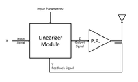
- FIG. 1 illustrates the power amplifier circuit with its linearizer module
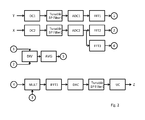
- FIG. 2 illustrates a first embodiment of the linearizer module with RF input signal
- a Linearizer Module (LM) within an embodiment of a Power Amplifier Circuit ( FIG. 1 ) is presented.
- This Linearizer Module connected with the input signal X (which can be digital signal or Radio Frequency (RF) signal, and can come from a modulator or a transmitter or a power amplifier driver), the output signal Z (which is a RF signal and enters into the power amplifier) and the feedback signal Y (which is a RF sample signal coming from the output of power amplifier).
- X which can be digital signal or Radio Frequency (RF) signal, and can come from a modulator or a transmitter or a power amplifier driver
- the output signal Z which is a RF signal and enters into the power amplifier
- the feedback signal Y which is a RF sample signal coming from the output of power amplifier
- This linearizer module can be implemented as a stand-alone module or an integrated module within a modulator or a transmitter.
- this linearizer module down-converts feedback RF signal Y (from power amplifier) into Intermediate Frequency (IF) band (module DC 1 in FIG. 2 ), and after filtering IF signal through a band-pass filter (module Tunable BP Filter 1 in FIG. 2 ), converts it into digital domain using an Analog-to-Digital (A/D) converter (module ADC 1 in FIG. 2 ). The result is feedback digital signal. Then using a FFT 1 (fast-Fourier transform) module converts the feedback digital signal into frequency-domain FB-FFT blocks.
- IF Intermediate Frequency
- A/D Analog-to-Digital
- this linearizer module converts input base-band RF signal X (from modulator) into Intermediate Frequency (IF) band (module DC 2 in FIG. 2 ), and after filtering IF signal through a band-pass filter (module Tunable BP Filter 2 in FIG. 2 ), converts it into digital domain using an Analog-to-Digital (A/D) converter (module ADC 2 in FIG. 2 ). The result is feed-forward input digital signal. Then using a FFT 2 module converts the feed-forward input digital signal into FF-FFT blocks. In the case the input to Linearizer Module is digital signal, the modules BP Filter 2 and ADC 2 are not needed.
- IF Intermediate Frequency
- A/D Analog-to-Digital
- FB-FFT blocks and FF-FFT blocks enter into a division module (DIV), in which FF-FFT blocks divide by FB-FFT blocks. Then the result of division goes through averaging module (AVG), and after averaging on at least 2 blocks, the result is CORR-COEF-FFT coefficients block which are being used for correcting and compensating linear and non-linear distortions of Power Amplifier.
- DIV division module
- AVG averageveraging module
- the feed-forward input digital signal is converted into FF-FFT blocks using FFT 3 module; and then elements of each block are being multiplied by CORR-COEF-FFT coefficients (in a point-by-point array multiplication method) as depicted in FIG. 2 , resulting in corrected digital signal CORR-SIG-FFT blocks.
- the corrected digital signal (CORR-SIG-FFT blocks) passes through a windowing module in frequency domain for achieving required spectrum masks of signal. Then, the windowed blocks pass IFFT module, and are converted into time domain (CORR-SIG).
- the corrected time-domain signal (CORR-SIG) is converted into analog using Digital-to-Analog converter (DAC module in FIG. 2 ).
- DAC module Digital-to-Analog converter
- the output passes Tunable BP filter, and then is up-converted to RF signal Z using UC module, which is the output of Linearizer Module.
Landscapes
- Engineering & Computer Science (AREA)
- Power Engineering (AREA)
- Microelectronics & Electronic Packaging (AREA)
- Physics & Mathematics (AREA)
- Nonlinear Science (AREA)
- Computer Networks & Wireless Communication (AREA)
- Signal Processing (AREA)
- Amplifiers (AREA)
Abstract
Description
- The present invention concerns the field of power amplifiers and in particular the enhancement of the performance of the amplifier by a feedback loop acting on the input signal. This invention can be used in each and every wireless communication transmitter, since there is definitely a power amplifier in the last part of the transmitter before the antenna, and every power amplifier has limited power performance (depending on type of modulation) due to its input-output curve. We are aiming to enhance the power utility of power amplifiers in different applications through introducing a new method of pre-distortion for mitigating linear and non-linear distortions of power amplifiers.
- Nowadays, there are many different methods for linearization of power amplifiers which generally use look-up-tables (LUT) and/or use off-line methods for training the coefficients and LUTs once. Also, there are many adaptive methods which constantly adapt the coefficients and data used for linearization. Currently, majority of these adaptive methods are developed in time-domain and generally need training signals (such as pre- and post-ambles in the signal). Moreover, almost based on all current methods you cannot build a stand-alone, plug-and-play module which can be used in variety of current applications.
- We are offering a novel method and system for linearization of PAs both in frequency domain and time domain, which can be implemented as a stand-alone plug-and-play module which is configurable, and is independent of many major parameters in wireless systems such as modulation, peak-to-average power ratio (PAPR) of the signal, and type of power amplifier (which is not the case in each and every other method presented so far).
- Power amplifier circuits (output stages) are classified as A, B, AB and C for analog designs, and class D and E for switching designs based upon the conduction angle or ‘angle of flow’ Θ of the input signal through the amplifying device, that is, the portion of the input signal cycle during which the amplifying device conducts. The image of the conduction angle is derived from amplifying a sinusoidal signal. (If the device is always on, Θ=360°.) The angle of flow is closely related to the amplifier power efficiency. The various classes are introduced below.
- 100% of the input signal is used (conduction angle Θ=360° or 2π, i.e. the active element works in its linear range all of the time). Where efficiency is not a consideration, most small signal linear amplifiers are designed as Class A, which means that the output devices are always in the conduction region. Class A amplifiers are typically more linear and less complex than other types, but are very inefficient. This type of amplifier is most commonly used in small-signal stages or for low-power applications (such as driving headphones).
- 50% of the input signal is used (Θ=180° or it, i.e. the active element works in its linear range half of the time and is more or less turned off for the other half). In most Class B, there are two output devices (or sets of output devices), each of which conducts alternately for exactly 180 deg (or half cycle) of the input signal; selective RF amplifiers can also be implemented using a single active element.
- These amplifiers are subject to crossover distortion if the handoff from one active element to the other is not perfect, as when two complimentary transistors (i.e. one PNP, one NPN) are connected as two emitter followers with their base and emitter terminals in common, requiring the base voltage to slew across the region where both devices are turned off.
- Here the two active elements conduct more than half of the time as a means to reduce the cross-over distortions of Class B amplifiers. In the example of the complementary emitter followers a bias network allows for more or less quiescent current thus providing an operating point somewhere between Class A and Class B. Sometimes a figure is added, e.g. AB1 or AB2, with higher figures implying a higher quiescent current and therefore more of the properties of Class A.
- Main article: These use switching to achieve a very high power efficiency (more than 90% in modern designs). By allowing each output device to be either fully on or off, losses are minimized. The analog output is created by pulse width modulation (PWM), i.e. the active element is switched on for shorter or longer intervals instead of modifying its resistor. There are more complicated switching schemes like sigma-delta modulation, to improve some performance aspects like lower distortions or better efficiency.
- There are several other amplifier classes, although they are mainly variations of the previous classes. For example, Class H and Class G amplifiers are marked by variation of the supply rails (in discrete steps or in a continuous fashion, respectively) following the input signal. Wasted heat on the output devices can be reduced as excess voltage is kept to a minimum. The amplifier that is fed with these rails itself can be of any class. These kinds of amplifiers are more complex, and are mainly used for specialized applications, such as very high-power units. Also, Class E and Class F amplifiers are commonly described in literature for radio frequencies applications where efficiency of the traditional classes deviate substantially from their ideal values. These classes use harmonic tuning of their output networks to achieve higher efficiency and can be considered a subset of Class C due to their conduction angle characteristics.
- Each and every RF power amplifier distorts the input signal when the input signal power reaches close to saturation level of PA. These distortions can be modeled as AM/AM and AM/PM distortions which have described in a lot of literatures of communication. In some applications such as in OFDM systems, because of sensitivity of receivers to these types of distortions, the designers of total communication system use the PA in a sufficient margin from its saturation point to make sure that the output signal is not distorted more than acceptable threshold. Using different methods of pre-distortion, this margin can be reduced and the power utility of PA can be increased.
- The present invention concerns a method for linearizing a power amplifier circuit having a digital base-band input signal, a power output signal, a power amplifier and a linearizer module (LM), this method comprising the steps of:
-
- extracting a feedback signal from the power amplifier (PA) output signal,
- down-converting the feedback RF-signal to feedback IF-signal,
- filtering the feedback IF-signal with a band-pass filter,
- A/D converting the filtered feedback IF-signal into a feedback digital signal,
- converting the feedback digital signal into frequency-domain using fast-Fourier transform FFT on a block of n-samples to obtain a feedback FB-FFT block,
- converting the input base-band digital signal into frequency-domain using fast-Fourier transform FFT on a block of n-samples to obtain a input FF-FFT block,
- dividing the input FF-FFT block with the feedback FB-FFT block to obtain FFT correction samples blocks,
- averaging at least two blocks of FFT correction samples to obtain FFT correction coefficient values,
- applying the FFT correction coefficient values to a digital complex multiplier,
- converting the output of the multiplier from frequency domain into time domain with an inverse FFT module to obtain a corrected digital input signal,
- Converting the corrected digital input signal to analog IF signal with a digital to analog converter to obtain a corrected IF input signal,
- applying the band-pass filter to the corrected IF input signal,
- up-converting the filtered corrected IF input signal to obtain a corrected RF input signal,
- applying the corrected RF input signal to the power amplifier.
- It is to be noted that n can be any integer number greater than 128, and sample is applied to show a discrete-time signal in digital domain.
- The present invention and its advantages will be better understood thanks to the enclosed detailed description of a particular embodiment and to the enclosed drawings, in which:
-
FIG. 1 illustrates the power amplifier circuit with its linearizer module, -
FIG. 2 illustrates a first embodiment of the linearizer module with RF input signal, - A Linearizer Module (LM) within an embodiment of a Power Amplifier Circuit (
FIG. 1 ) is presented. This Linearizer Module connected with the input signal X (which can be digital signal or Radio Frequency (RF) signal, and can come from a modulator or a transmitter or a power amplifier driver), the output signal Z (which is a RF signal and enters into the power amplifier) and the feedback signal Y (which is a RF sample signal coming from the output of power amplifier). - This linearizer module can be implemented as a stand-alone module or an integrated module within a modulator or a transmitter.
- As depicted in
FIG. 2 , this linearizer module down-converts feedback RF signal Y (from power amplifier) into Intermediate Frequency (IF) band (module DC1 inFIG. 2 ), and after filtering IF signal through a band-pass filter (module Tunable BP Filter1 inFIG. 2 ), converts it into digital domain using an Analog-to-Digital (A/D) converter (module ADC1 inFIG. 2 ). The result is feedback digital signal. Then using a FFT1 (fast-Fourier transform) module converts the feedback digital signal into frequency-domain FB-FFT blocks. - As depicted in
FIG. 2 , this linearizer module converts input base-band RF signal X (from modulator) into Intermediate Frequency (IF) band (module DC2 inFIG. 2 ), and after filtering IF signal through a band-pass filter (module Tunable BP Filter2 inFIG. 2 ), converts it into digital domain using an Analog-to-Digital (A/D) converter (module ADC2 inFIG. 2 ). The result is feed-forward input digital signal. Then using a FFT2 module converts the feed-forward input digital signal into FF-FFT blocks. In the case the input to Linearizer Module is digital signal, the modules BP Filter2 and ADC2 are not needed. - Then, as depicted in
FIG. 2 , FB-FFT blocks and FF-FFT blocks enter into a division module (DIV), in which FF-FFT blocks divide by FB-FFT blocks. Then the result of division goes through averaging module (AVG), and after averaging on at least 2 blocks, the result is CORR-COEF-FFT coefficients block which are being used for correcting and compensating linear and non-linear distortions of Power Amplifier. - The feed-forward input digital signal is converted into FF-FFT blocks using FFT3 module; and then elements of each block are being multiplied by CORR-COEF-FFT coefficients (in a point-by-point array multiplication method) as depicted in
FIG. 2 , resulting in corrected digital signal CORR-SIG-FFT blocks. Now, the corrected digital signal (CORR-SIG-FFT blocks) passes through a windowing module in frequency domain for achieving required spectrum masks of signal. Then, the windowed blocks pass IFFT module, and are converted into time domain (CORR-SIG). - The corrected time-domain signal (CORR-SIG) is converted into analog using Digital-to-Analog converter (DAC module in
FIG. 2 ). The output passes Tunable BP filter, and then is up-converted to RF signal Z using UC module, which is the output of Linearizer Module.
Claims (11)
Priority Applications (1)
| Application Number | Priority Date | Filing Date | Title |
|---|---|---|---|
| US13/509,893 US8542062B2 (en) | 2009-11-16 | 2010-11-16 | Adaptive digital pre-distortion method and device to enhance the power utility of power amplifiers in wireless digital communication applications |
Applications Claiming Priority (3)
| Application Number | Priority Date | Filing Date | Title |
|---|---|---|---|
| US28124109P | 2009-11-16 | 2009-11-16 | |
| US13/509,893 US8542062B2 (en) | 2009-11-16 | 2010-11-16 | Adaptive digital pre-distortion method and device to enhance the power utility of power amplifiers in wireless digital communication applications |
| PCT/EP2010/067611 WO2011058197A1 (en) | 2009-11-16 | 2010-11-16 | An adaptive digital pre-distortion method and device to enhance the power utility of power amplifiers in wireless digital communication applications |
Publications (2)
| Publication Number | Publication Date |
|---|---|
| US20120249233A1 true US20120249233A1 (en) | 2012-10-04 |
| US8542062B2 US8542062B2 (en) | 2013-09-24 |
Family
ID=43500289
Family Applications (1)
| Application Number | Title | Priority Date | Filing Date |
|---|---|---|---|
| US13/509,893 Expired - Fee Related US8542062B2 (en) | 2009-11-16 | 2010-11-16 | Adaptive digital pre-distortion method and device to enhance the power utility of power amplifiers in wireless digital communication applications |
Country Status (3)
| Country | Link |
|---|---|
| US (1) | US8542062B2 (en) |
| EP (1) | EP2502345A1 (en) |
| WO (1) | WO2011058197A1 (en) |
Cited By (5)
| Publication number | Priority date | Publication date | Assignee | Title |
|---|---|---|---|---|
| US20160165562A1 (en) * | 2014-12-08 | 2016-06-09 | Nextnav, Llc | Systems and methods for selectively receiving and processing rf signals at an rf beacon |
| US20190013890A1 (en) * | 2016-01-08 | 2019-01-10 | Kyoto University | Transmitter, transmission method, and receiver |
| US10231201B2 (en) | 2014-12-08 | 2019-03-12 | Nextnav, Llc | Systems and methods for assured time synchronization of an RF beacon |
| CN112042118A (en) * | 2018-04-25 | 2020-12-04 | 乌帕泰克 | System and method for baseband linearization of class-G radio frequency power amplifiers |
| US12546902B2 (en) | 2022-10-28 | 2026-02-10 | Nextnav, Llc | Hybrid position navigation and timing system |
Families Citing this family (2)
| Publication number | Priority date | Publication date | Assignee | Title |
|---|---|---|---|---|
| US9702907B2 (en) * | 2011-12-16 | 2017-07-11 | Tektronix, Inc. | Frequency mask trigger with non-uniform bandwidth segments |
| FR3076135B1 (en) * | 2017-12-21 | 2019-12-27 | Thales | LOW COMPLEXITY TIME SYNCRONIZATION IN A DIGITAL PREDISTORSION CALCULATION LOOP |
Citations (1)
| Publication number | Priority date | Publication date | Assignee | Title |
|---|---|---|---|---|
| US7035345B2 (en) * | 2001-06-08 | 2006-04-25 | Polyvalor S.E.C. | Adaptive predistortion device and method using digital receiver |
Family Cites Families (11)
| Publication number | Priority date | Publication date | Assignee | Title |
|---|---|---|---|---|
| GB2351624B (en) | 1999-06-30 | 2003-12-03 | Wireless Systems Int Ltd | Reducing distortion of signals |
| US6798843B1 (en) | 1999-07-13 | 2004-09-28 | Pmc-Sierra, Inc. | Wideband digital predistortion linearizer for nonlinear amplifiers |
| GB2359432B (en) | 2000-02-17 | 2002-07-03 | Wireless Systems Int Ltd | Signal detection |
| US6275106B1 (en) | 2000-02-25 | 2001-08-14 | Spectrian Corporation | Spectral distortion monitor for controlling pre-distortion and feed-forward linearization of rf power amplifier |
| JP4015455B2 (en) | 2002-03-29 | 2007-11-28 | 富士通株式会社 | Distortion compensation device |
| KR100480278B1 (en) | 2002-12-24 | 2005-04-07 | 삼성전자주식회사 | Digital predistorter of a wideband power amplifier and adaptation method therefor |
| JP4033794B2 (en) | 2003-03-24 | 2008-01-16 | 株式会社エヌ・ティ・ティ・ドコモ | High efficiency linear power amplifier |
| CN100589475C (en) | 2003-04-21 | 2010-02-10 | Rgb网络有限公司 | Broadband Multi-channel Quadrature Amplitude Modulation of CATV Signals |
| CN101023578B (en) * | 2004-09-21 | 2010-04-21 | 株式会社日立国际电气 | Distortion compensation amplifying device |
| WO2006082681A1 (en) * | 2005-02-01 | 2006-08-10 | Hitachi Kokusai Electric Inc. | Spectrum analysis method, distortion detection device, and distortion compensation amplification device |
| WO2007046370A1 (en) | 2005-10-17 | 2007-04-26 | Hitachi Kokusai Electric Inc. | Non-linear distortion detection method and distortion compensation amplification device |
-
2010
- 2010-11-16 US US13/509,893 patent/US8542062B2/en not_active Expired - Fee Related
- 2010-11-16 EP EP10790904A patent/EP2502345A1/en not_active Withdrawn
- 2010-11-16 WO PCT/EP2010/067611 patent/WO2011058197A1/en not_active Ceased
Patent Citations (1)
| Publication number | Priority date | Publication date | Assignee | Title |
|---|---|---|---|---|
| US7035345B2 (en) * | 2001-06-08 | 2006-04-25 | Polyvalor S.E.C. | Adaptive predistortion device and method using digital receiver |
Cited By (7)
| Publication number | Priority date | Publication date | Assignee | Title |
|---|---|---|---|---|
| US20160165562A1 (en) * | 2014-12-08 | 2016-06-09 | Nextnav, Llc | Systems and methods for selectively receiving and processing rf signals at an rf beacon |
| US9967845B2 (en) * | 2014-12-08 | 2018-05-08 | Nextnav, Llc | Systems and methods for selectively receiving and processing RF signals at an RF beacon |
| US10231201B2 (en) | 2014-12-08 | 2019-03-12 | Nextnav, Llc | Systems and methods for assured time synchronization of an RF beacon |
| US20190013890A1 (en) * | 2016-01-08 | 2019-01-10 | Kyoto University | Transmitter, transmission method, and receiver |
| US10581546B2 (en) * | 2016-01-08 | 2020-03-03 | Kyoto University | Transmitter, transmission method, and receiver based on time-domain windows |
| CN112042118A (en) * | 2018-04-25 | 2020-12-04 | 乌帕泰克 | System and method for baseband linearization of class-G radio frequency power amplifiers |
| US12546902B2 (en) | 2022-10-28 | 2026-02-10 | Nextnav, Llc | Hybrid position navigation and timing system |
Also Published As
| Publication number | Publication date |
|---|---|
| WO2011058197A1 (en) | 2011-05-19 |
| US8542062B2 (en) | 2013-09-24 |
| EP2502345A1 (en) | 2012-09-26 |
Similar Documents
| Publication | Publication Date | Title |
|---|---|---|
| US8417197B2 (en) | Pre-distortion method and device to enhance the power utility of power amplifiers in wireless digital communication applications | |
| US12176934B2 (en) | Predistortion circuit, method for generating a predistorted baseband signal, control circuit for a predistortion circuit, method to determine parameters for a predistortion circuit, and apparatus and method for predistorting a baseband signal | |
| US8542062B2 (en) | Adaptive digital pre-distortion method and device to enhance the power utility of power amplifiers in wireless digital communication applications | |
| US9490754B2 (en) | High-frequency drain power supply to decrease power dissipation in class-AB power amplifiers | |
| US8649745B2 (en) | Adaptive predistortion for a non-linear subsystem based on a model as a concatenation of a non-linear model followed by a linear model | |
| CN102460385B (en) | Long-range can allocating power amplifier system and method again | |
| CN102948071A (en) | Modulation agnostic digital hybrid mode power amplifier system and method | |
| JP2010525758A (en) | Digital hybrid mode power amplifier system | |
| CN103715997A (en) | Circuit capable of improving linearity of power amplifier | |
| CN104704747A (en) | Extended bandwidth digital doherty transmitter | |
| CN101512895B (en) | Amplifier architecture for polar modulation | |
| Kardaras et al. | Advanced multimode radio for wireless & mobile broadband communication | |
| EP1649594A1 (en) | Amplifying circuit comprising an envelope modulated limit cycles modulator circuit | |
| EP2375565A1 (en) | Bias circuit design for bipolar power amplifier linearity improvement | |
| WO2013093862A2 (en) | Architecture of a low bandwidth predistortion system for non-linear rf components | |
| Choi et al. | 28.8 dBm, high efficiency, linear GaN power amplifier with in-phase power combining for IEEE 802.11 p applications | |
| Xu et al. | A digital combining applied to the multilevel pulse modulated polar transmitter | |
| Seegerer et al. | EDGE transmitter with commercial GSM power amplifier using polar modulation with memory predistortion | |
| WO2016071888A1 (en) | An amplifier system for amplifying an rf signal | |
| CN203788248U (en) | Circuit for improving linearity of power amplifier | |
| EP2846460A1 (en) | Arrangement and method for radio frequency power amplification | |
| Wang | Baseband linearization schemes for high efficiency power amplifiers | |
| Hoyerby et al. | Band-split forward-path Cartesian feedback for multicarrier TETRA RF power amplifiers | |
| Ghannouchi | An S band RF digital linearizer for TWTAs and SSPAs | |
| Ren et al. | Adaptive digital predistorter with improving feedback signal distortion over-compensation |
Legal Events
| Date | Code | Title | Description |
|---|---|---|---|
| AS | Assignment |
Owner name: INNOVARADIO SA, SWITZERLAND Free format text: ASSIGNMENT OF ASSIGNORS INTEREST;ASSIGNORS:FARAHANI SAMANI, AMIRHOOSHANG;HEZAVEH, JEYRAN;TALEBI, ALI;SIGNING DATES FROM 20120507 TO 20120511;REEL/FRAME:028318/0057 |
|
| FEPP | Fee payment procedure |
Free format text: PAYOR NUMBER ASSIGNED (ORIGINAL EVENT CODE: ASPN); ENTITY STATUS OF PATENT OWNER: SMALL ENTITY |
|
| REMI | Maintenance fee reminder mailed | ||
| LAPS | Lapse for failure to pay maintenance fees |
Free format text: PATENT EXPIRED FOR FAILURE TO PAY MAINTENANCE FEES (ORIGINAL EVENT CODE: EXP.) |
|
| STCH | Information on status: patent discontinuation |
Free format text: PATENT EXPIRED DUE TO NONPAYMENT OF MAINTENANCE FEES UNDER 37 CFR 1.362 |
|
| FP | Lapsed due to failure to pay maintenance fee |
Effective date: 20170924 |