US20120249012A1 - Method and system for supplying multiple led drivers using the same traic dimmer - Google Patents
Method and system for supplying multiple led drivers using the same traic dimmer Download PDFInfo
- Publication number
- US20120249012A1 US20120249012A1 US13/075,200 US201113075200A US2012249012A1 US 20120249012 A1 US20120249012 A1 US 20120249012A1 US 201113075200 A US201113075200 A US 201113075200A US 2012249012 A1 US2012249012 A1 US 2012249012A1
- Authority
- US
- United States
- Prior art keywords
- rcd
- absorption circuit
- transient absorption
- resistor
- power
- Prior art date
- Legal status (The legal status is an assumption and is not a legal conclusion. Google has not performed a legal analysis and makes no representation as to the accuracy of the status listed.)
- Abandoned
Links
- 238000000034 method Methods 0.000 title claims description 9
- 230000001052 transient effect Effects 0.000 claims abstract description 56
- 238000010521 absorption reaction Methods 0.000 claims abstract description 55
- 239000003990 capacitor Substances 0.000 claims abstract description 27
- 238000009966 trimming Methods 0.000 claims abstract description 18
- 238000004804 winding Methods 0.000 claims description 10
- 101100299489 Oryza sativa subsp. japonica PTD gene Proteins 0.000 description 8
- 101100136621 Petunia hybrida PT4 gene Proteins 0.000 description 8
- 238000010586 diagram Methods 0.000 description 5
- 230000005611 electricity Effects 0.000 description 3
- 238000012986 modification Methods 0.000 description 3
- 230000004048 modification Effects 0.000 description 3
- 238000007792 addition Methods 0.000 description 2
- 238000005516 engineering process Methods 0.000 description 2
- 238000005286 illumination Methods 0.000 description 2
- 238000003491 array Methods 0.000 description 1
- 238000006243 chemical reaction Methods 0.000 description 1
- 238000001914 filtration Methods 0.000 description 1
- 239000000463 material Substances 0.000 description 1
- 230000007935 neutral effect Effects 0.000 description 1
- 239000004065 semiconductor Substances 0.000 description 1
- 238000006467 substitution reaction Methods 0.000 description 1
- 230000000007 visual effect Effects 0.000 description 1
Images


Classifications
-
- H—ELECTRICITY
- H02—GENERATION; CONVERSION OR DISTRIBUTION OF ELECTRIC POWER
- H02M—APPARATUS FOR CONVERSION BETWEEN AC AND AC, BETWEEN AC AND DC, OR BETWEEN DC AND DC, AND FOR USE WITH MAINS OR SIMILAR POWER SUPPLY SYSTEMS; CONVERSION OF DC OR AC INPUT POWER INTO SURGE OUTPUT POWER; CONTROL OR REGULATION THEREOF
- H02M5/00—Conversion of AC power input into AC power output, e.g. for change of voltage, for change of frequency, for change of number of phases
- H02M5/02—Conversion of AC power input into AC power output, e.g. for change of voltage, for change of frequency, for change of number of phases without intermediate conversion into DC
- H02M5/04—Conversion of AC power input into AC power output, e.g. for change of voltage, for change of frequency, for change of number of phases without intermediate conversion into DC by static converters
- H02M5/22—Conversion of AC power input into AC power output, e.g. for change of voltage, for change of frequency, for change of number of phases without intermediate conversion into DC by static converters using discharge tubes with control electrode or semiconductor devices with control electrode
- H02M5/25—Conversion of AC power input into AC power output, e.g. for change of voltage, for change of frequency, for change of number of phases without intermediate conversion into DC by static converters using discharge tubes with control electrode or semiconductor devices with control electrode using devices of a thyratron or thyristor type requiring extinguishing means
- H02M5/257—Conversion of AC power input into AC power output, e.g. for change of voltage, for change of frequency, for change of number of phases without intermediate conversion into DC by static converters using discharge tubes with control electrode or semiconductor devices with control electrode using devices of a thyratron or thyristor type requiring extinguishing means using semiconductor devices only
-
- H—ELECTRICITY
- H05—ELECTRIC TECHNIQUES NOT OTHERWISE PROVIDED FOR
- H05B—ELECTRIC HEATING; ELECTRIC LIGHT SOURCES NOT OTHERWISE PROVIDED FOR; CIRCUIT ARRANGEMENTS FOR ELECTRIC LIGHT SOURCES, IN GENERAL
- H05B45/00—Circuit arrangements for operating light-emitting diodes [LED]
- H05B45/30—Driver circuits
- H05B45/37—Converter circuits
- H05B45/3725—Switched mode power supply [SMPS]
- H05B45/385—Switched mode power supply [SMPS] using flyback topology
Definitions
- the present invention relates generally to light emitting diode (LED) drivers. More specifically, the present invention relates to a dimmable lighting LED driver system and a method of dimming thereof. Still more specifically, the present invention is related to the use of the same triode for alternating current (TRIAC) dimmer to control the dimming of a plurality of LED drivers.
- TRIAC alternating current
- LED light emitting diode
- LEDs are a type of semiconductor device requiring direct current (DC) electricity input source for operation.
- Conventional LED lighting unit comprises a LED driver power supply, a dimming module, a dimming controller panel, and arrays of LEDs.
- the LED driver power supply takes an external electricity power input source and convert to a constant direct current output, feeding the dimming module and in turn the LEDs.
- the external power source is usually an alternative current electricity power source.
- LED driver power supply one limitation is that the choice of LED driver power supply used must be carefully matched with the capacity of the LEDs, as the maximum current driving the LEDs is fixed by the LED driver power supply based on its type and capacity.
- TRIAC triode for alternating current
- FIG. 1 depicts the use of a TRIAC dimmer to perform the light-dimming operation via the control of input power to a plurality of LED drivers, each of which includes a flyback switching-mode power supply (not shown in the figure).
- the power inputs of the plurality of LED drivers are connected in parallel to form a single source of power input, and this single source of power input is in turn connected in series to the TRIAC dimmer.
- the function of the TRIAC dimmer is to modulate the conduction angle of the AC input voltage, making the LED drivers connected thereafter change the output current levels accordingly. Dimming can be achieved as the output current is used to drive the LED in a lamp and the current level determines the brightness of the LED.
- the TRIAC dimmer is connected to the Live (L) of the AC input.
- the power supply common to all LED drivers is coupled to the other end of the TRIAC dimmer and the Neutral (N) of the AC input.
- the voltage of the power supply common to all LED drivers also changes.
- the LED driver begins to operate. At that time, the output voltage levels of all the LED drivers do not reach the threshold voltage required for LEDs to light up. The LEDs do not glow.
- the power input to LED drivers also increases. When the output voltage of a LED driver reaches the threshold voltage, the LED begins to glow. At that time, the LED driver is still working in an open-loop condition, and the feedback control circuit does not work.
- the conduction angle of the TRIAC dimmer increases so that the output voltage level of the LED driver also increases, the output current reaches the full-load current condition required for the LED. Afterwards, the LED driver operates in a closed-loop mode. The control circuit comes into operation. It is possible to adjust the output current based on the control circuit. The luminance of the LED reaches the maximum value. At that time, increasing the conduction angle of the TRIAC dimmer does not change the luminance of the LED. However, in the presence of multiple LED drivers using the same TRIAC dimmer as shown in FIG.
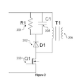
- FIG. 2 is a transient absorption circuit installed in a LED driver, according to the state of the art.
- This circuit comprises a resistor, a capacitor, and a diode, the circuit being referred to as an RCD transient absorption circuit.
- the resistor R 1 201 and the capacitor C 1 204 are connected in parallel, followed by connecting the resultant unit to a diode D 1 202 in series.
- One winding of the transformer T 1 205 is connected in parallel to the unit formed by the three aforementioned components, and in series to the switcher Q 1 203 .
- the other winding of the transformer T 1 205 is connected to the output section of the LED driver (not shown in the figure).
- the RCD transient absorption circuit is connected with the full-wave bridge rectifier (not shown in the figure).
- the function of the RCD transient absorption circuit is illustrated as follows. When the flyback switching mode power supply is operating, and when the switcher Q 1 203 is turning off, the inductance of the transformer can lead to a high peak voltage.
- the RCD transient absorption circuit is used to absorb this voltage peak in order to protect the switcher Q 1 203 from being punched through by the high voltage. Note that if the switcher Q 1 203 is punched through, the whole LED driver cannot properly work. In the start-up phase and in the low-load condition, the RCD transient absorption circuit is the main source of power loss. Since the RCD transient absorption circuit in the state of the art does not incorporate a function of controlling the power loss, it follows that the LEDs powered by different LED drivers cannot achieve uniformity in the start-up time and in luminance.
- the presently claimed invention provides a dimmable LED driver system that incorporates an RCD transient absorption circuit, and a method of light dimming.
- the presently claimed invention overcome the problem of start-up time misalignment in the presence of multiple LED drivers, where this misalignment causes the problem of LEDs not glowing up at the same time and not having the same luminance.
- the RCD transient absorption circuit comprises a first resistor, a capacitor and a diode.
- the first resistor is connected in parallel to the capacitor followed by connecting the resultant unit in series with the diode, wherein: one end of the unit formed by connecting in parallel the first resistor and the capacitor is connected to the cathode of the diode; another end of this unit is the first port of the RCD transient absorption circuit; and the anode of the diode is the second port of this RCD transient absorption circuit.
- the RCD transient absorption circuit further comprises a power-trimming device, which is connected in parallel to the first resistor and the capacitor.
- the presently claimed invention also provides a dimmable LED driver system that allows the dimming function to be controlled by a dimmer therein.
- the dimmable LED driver system comprises a dimmer and at least one LED driver.
- the LED driver comprises: an AC-to-DC converter that matches the characteristics of the dimmer; a transformer for storing energy and for changing the voltage level; an output section for supplying power to LED(s) for the lighting purpose; and a pulse-width-modulation (PWM) controller and a switcher, both of which are used for control of the output power.
- PWM pulse-width-modulation
- the aforementioned LED driver uses the RCD transient absorption circuit disclosed in the present invention, where the first and the second ports of the RCD transient absorption circuit are connected to the two ports of the primary winding of the transformer, and the aforementioned first port is connected to the output of the AC-to-DC converter.
- the presently claimed invention also provides a method that employs a dimmer to perform the dimming function on LED drivers.
- This method comprises: installing the RCD transient absorption circuit disclosed in the present invention into each of the plurality of LED drivers; choosing one LED driver as the reference driver, and setting the conduction angle of the dimmer such that the reference driver delivers an output current that is 1% within the full-load current; measuring the output current levels of LED drivers other than the reference driver; and adjusting the power-trimming device of the RCD transient absorption circuit in each of the LED drivers such that the output current is the same as that of the reference driver.
- the advantage of this invention is summarized as follows. Using the dimmable LED driver system that employs the disclosed RCD transient absorption circuit enables one to adjust the start-up output power level. It follows that the output current levels delivered from multiple LED drivers can be made the same, thus enabling different LEDs to glow up at the same time.
- FIG. 1 is a schematic diagram showing the use of a TRIAC dimmer to perform the dimming operation on a plurality of LED drivers;
- FIG. 2 shows a transient absorption circuit used in a LED driver according to the state of the art
- FIG. 3 shows a RCD transient absorption circuit according to the first embodiment of the presently claimed invention
- FIG. 4 shows a RCD transient absorption circuit according to the second embodiment of the presently claimed invention.
- FIG. 5 is a circuit diagram for a TRIAC dimmer and a LED driver realized according to the second embodiment of the presently claimed invention, the LED driver serving the purpose of an example for illustration.
- the presently claimed invention operates by adjusting the power loss to control the output power level, and overcomes the problem of unsynchronized start-up time and unequal luminance levels caused by different power losses among different LED drivers.
- the presently claimed invention achieves the desired result that the LEDs give out their light synchronously at the start-up time and produce the light at the same luminance level.
- the components having higher losses are the MOS switcher, transformer, rectifier diode, and RCD transient absorption circuit. Therefore, the main approach of the presently claimed invention is to modify the RCD transient absorption circuit in order to control the power loss.
- a power-trimming device PTD 1 300 , resistor R 1 303 and capacitor C 1 304 are connected in parallel, and the resultant combined unit is serially connected to cathode of diode D 1 305 .
- the unit formed by the aforesaid four components: power-trimming device PTD 1 300 , resistor R 1 303 , capacitor C 1 304 , and the diode D 1 305 is connected in parallel to a winding of transformer T 1 307 .
- one port of the winding of transformer T 1 307 is connected to power-trimming device PTD 1 300 , resistor R 1 303 and capacitor C 1 304 ; and the other port is connected to the anode of diode D 1 305 .
- the other winding of transformer T 1 307 is connected to the output section of the LED driver (not shown in the figure).
- This RCD transient absorption circuit is connected to a full-wave bridge rectifier (not shown), serving the purpose of AC-to-DC conversion.
- power-trimming device PTD 1 300 is the serially connected cascade of variable resistor VR 1 302 and protection resistor R 2 301 .
- This power-trimming device PTD 1 is connected in parallel to resistor R 1 303 , and capacitor C 1 304 .
- the function of the RCD transient absorption circuit is to absorb the voltage peak occurred at switcher Q 1 306 in order to prevent it from being punched through.
- the resistance range of variable resistor VR 1 302 is normally from a few 10 k ohms to some 100 k ohms, determined according to: the inductance value of transformer T 1 307 ; the values of resistor R 1 303 , capacitor C 1 304 , and diode D 1 305 ; and the variation of the power input to the LED driver.
- the addition of protection resistor R 2 301 in the embodiment is to prevent any mistaken operation on variable resistor VR 1 302 .
- variable resistor VR 1 302 Even if variable resistor VR 1 302 is mistakenly adjusted to zero ohm, neither variable resistor VR 1 302 nor the rest of the circuit will be damaged.
- protection resistor R 2 301 is in the range of a few 10 k ohms.
- resistors R 1 303 , capacitor C 1 304 , and diode D 1 305 are commonly used components in existing transient absorption circuits.
- Switcher Q 1 306 can be any component that can achieve its purpose. Switcher Q 1 306 can be a MOSFET or a triode.
- the drain is connected to the anode of diode D 1 305
- the source is connected to a full-wave bridge rectifier (not shown)
- the gate is connected to a PWM controller (not shown).
- the PWM controller controls the output section of the LED driver through the feedback network.
- One embodiment of this invention is therefore a power trimming device comprising a variable resistor only.
- variable resistor VR 1 302 In a system with a plurality of LED drivers, one of them is chosen as a reference driver. When a driver has an output current greater than that of the reference driver during the start-up stage, the value of variable resistor VR 1 302 can be reduced; otherwise, its value can be increased.
- the function of variable resistor VR 1 302 is to change the power loss of the circuit in order to change the output power at the start-up time. It is based on the following formula:
- P in P loss +P out , where P in is the input power, P loss is the power loss, and P out is the output power.
- P in is a normally a constant.
- the RCD transient absorption circuit detailed in this embodiment is particularly suitable for the following situations: when the output power is small, for example, when the output power is less than 15 W; or when the inductance value of transformer T 1 307 is small, for example, if it is less than 15 ⁇ H.
- FIG. 4 Referring to the diagram of the RCD transient absorption circuit as shown in FIG. 4 .
- a transient voltage suppressor TVS
- PTD 1 400 Apart from power-trimming device PTD 1 400 , resistor R 1 403 and capacitor C 1 404 as illustrated in FIG. 3 , one can insert a transient voltage suppressor (TVS), which is connected in parallel to power-trimming device PTD 1 400 , resistor R 1 403 and capacitor C 1 404 with the additional requirement that the cathode of the TVS 408 is also connected to cathode of the diode D 1 405 .
- TVS transient voltage suppressor
- the TVS 408 is connected in parallel to: the cascade of variable resistor VR 1 402 in series with protection resistor R 2 401 ; resistor R 1 403 ; and capacitor C 1 404 .
- the working principle of this RCD transient absorption circuit is similar to that of the first embodiment.
- the parameters of the additional TVS 408 are determined according to the inductance and the clamped voltage. When a high-energy impulse appears, the function of the TVS 408 is to reduce its conductance to a low value in order to allow a larger current to pass and at the same time clamp the voltage to a predetermined level. When under the no-load or light-load condition, the TVS 408 does not work.
- diode D 1 405 , resistor R 1 403 , protection resistor R 2 401 , variable resistor VR 1 402 and capacitor C 1 404 clamp and adjust the power loss.
- the TVS 408 functions and ensures that the peak voltage does not damage switcher Q 1 406 .
- the second embodiment for the RCD transient absorption circuit is especially suitable for use in the situation that the output power is large or that the inductance value of transformer T 1 407 is large. In this situation, a capacitor with a small capacitance value can be used for capacitor C 1 404 in order to reduce the loss.
- FIG. 5 is a circuit diagram showing a TRIAC dimmer and an example LED driver realized according to the second embodiment of the presently claimed invention.
- the AC input is connected to the AC-to-DC converter via a TRIAC dimmer.
- a preferred realization of the AC-to-DC converter is a full-wave bridge rectifier.
- the electric power from the output of the AC-to-DC converter is fed to the primary winding of the transformer.
- the secondary winding of the transformer is connected to the output section.
- the end of the output section is connected to a group of series-connected LEDs. Note that the output section performs rectification and filtering on the power obtained from the transformer. It is also noticed that the RCD transient absorption circuit is connected to the primary winding of the transformer.
- the PWM controller is used to control the switcher, and it can be realized by any IC under the relevant category, for example: SSL 2101 and SSL 2102 .
- the PWM controller is connected to the output section via a feedback network, wherein the feedback network is a feedback loop for ensuring the stability of the circuit.
- the feedback network is a feedback loop for ensuring the stability of the circuit.
- the tolerance levels of components are required to be at least better than: 1% for resistor R 1 402 and protection resistor R 2 401 ; 10% for variable resistor VR 1 403 , and 10% for capacitor C 1 404 .
- the value of resistor R 1 402 is usually greater than that of protection resistor R 2 401 , a larger value of R 1 402 being able to ensure proper working of the circuit.
- the current taken up by a LED driver realized by existing technology varies between less than 1 mA to 6 mA.
- the output currents during start-up viz., the current passing through LED 1 405 and LED 2 406 , maintain at a rather constant value within the aforementioned range. Since the variation of the current level is relatively small, it can maintain the output current levels at Io*1% ⁇ 20% where Io is the full-load output current. For example, when the output current is 350 mA, the output current at start-up can be maintained within a range of 2.8-4.2 mA. The stability of output current levels ensures that the LEDs start to glow at the same time and have the same luminance level.
- the presently claimed invention provides a method to employ a TRIAC dimmer to control LED drivers. Under the same condition of supply voltage, adjust the conduction angle of the TRIAC dimmer such that the output current of a reference LED driver is 1% of the full-load current. Fixing this conduction angle, one can adjust variable resistor VR 1 403 of another LED driver in order that the output current provided to the LED is the same as that of the reference driver.
Landscapes
- Engineering & Computer Science (AREA)
- Power Engineering (AREA)
- Circuit Arrangement For Electric Light Sources In General (AREA)
Abstract
An RCD transient absorption circuit, having a first port and a second port, the RCD transient absorption circuit comprising a first resistor, a capacitor and a diode, wherein: the first resistor is connected in parallel to the capacitor, and resultant parallel connection of which is connected in series to a diode; one end of the resultant parallel connection of the first resistor and the capacitor is connected to a cathode of the diode; another end of resultant parallel connection is the first port of the RCD transient absorption circuit; and the second port of the RCD transient absorption circuit is an anode of the diode; the RCD transient absorption circuit further comprises a power-trimming device connected in parallel to the first resistor and the capacitor.
Description
- A portion of the disclosure of this patent document contains material, which is subject to copyright protection. The copyright owner has no objection to the facsimile reproduction by anyone of the patent document or the patent disclosure, as it appears in the Patent and Trademark Office patent file or records, but otherwise reserves all copyright rights whatsoever.
- This application claims priority under 35 U.S.C. §119 to the China patent application 201110040964.5, filed Feb. 18, 2011, the disclosure of which is incorporated herein by reference.
- The present invention relates generally to light emitting diode (LED) drivers. More specifically, the present invention relates to a dimmable lighting LED driver system and a method of dimming thereof. Still more specifically, the present invention is related to the use of the same triode for alternating current (TRIAC) dimmer to control the dimming of a plurality of LED drivers.
- Traditionally, incandescent and fluorescent lights have been the primary source of artificial illumination. However, significant advances in the light emitting diode (LED) technology have made the light output of LEDs not only for indicator applications but also sufficient for general illumination.
- LEDs are a type of semiconductor device requiring direct current (DC) electricity input source for operation. Conventional LED lighting unit comprises a LED driver power supply, a dimming module, a dimming controller panel, and arrays of LEDs. The LED driver power supply takes an external electricity power input source and convert to a constant direct current output, feeding the dimming module and in turn the LEDs. For land and building use, the external power source is usually an alternative current electricity power source. In such conventional LED lighting unit, one limitation is that the choice of LED driver power supply used must be carefully matched with the capacity of the LEDs, as the maximum current driving the LEDs is fixed by the LED driver power supply based on its type and capacity.
- One common type of dimming module is the triode for alternating current (TRIAC) dimmer. Traditionally, one TRIAC dimmer is paired with one LED driver.
-
FIG. 1 depicts the use of a TRIAC dimmer to perform the light-dimming operation via the control of input power to a plurality of LED drivers, each of which includes a flyback switching-mode power supply (not shown in the figure). In the system, the power inputs of the plurality of LED drivers are connected in parallel to form a single source of power input, and this single source of power input is in turn connected in series to the TRIAC dimmer. The function of the TRIAC dimmer is to modulate the conduction angle of the AC input voltage, making the LED drivers connected thereafter change the output current levels accordingly. Dimming can be achieved as the output current is used to drive the LED in a lamp and the current level determines the brightness of the LED. One end of the TRIAC dimmer is connected to the Live (L) of the AC input. The power supply common to all LED drivers is coupled to the other end of the TRIAC dimmer and the Neutral (N) of the AC input. Although dimming can be achieved by the arrangement shown inFIG. 1 , a major problem is that the start-up times for LEDs controlled by different LED drivers are not the same. The start-up time is the time that the LED starts to give out its light. - As the conduction angle of the TRIAC dimmer changes, the voltage of the power supply common to all LED drivers also changes. When the voltage increases to the working voltage of the LED driver integrated circuit (IC) in a LED driver, the LED driver begins to operate. At that time, the output voltage levels of all the LED drivers do not reach the threshold voltage required for LEDs to light up. The LEDs do not glow. As the conduction angle of the TRIAC dimmer increases, the power input to LED drivers also increases. When the output voltage of a LED driver reaches the threshold voltage, the LED begins to glow. At that time, the LED driver is still working in an open-loop condition, and the feedback control circuit does not work. When the conduction angle of the TRIAC dimmer increases so that the output voltage level of the LED driver also increases, the output current reaches the full-load current condition required for the LED. Afterwards, the LED driver operates in a closed-loop mode. The control circuit comes into operation. It is possible to adjust the output current based on the control circuit. The luminance of the LED reaches the maximum value. At that time, increasing the conduction angle of the TRIAC dimmer does not change the luminance of the LED. However, in the presence of multiple LED drivers using the same TRIAC dimmer as shown in
FIG. 1 , and when these LED drivers are working in the open-loop mode, it is noticed that variation in component parameters (namely, difference between the actual value and the nominal value of a component) for the LED drivers leads to different power dissipation levels in the circuits. It follows that the actual power outputs of the LED drivers are not the same and the output current levels are also not the same. This variation of output current levels leads to the visual effect that some of LEDs glow up first and some of LEDs glow up later. That is, the LEDs driven by different LED drivers do not start to glow at the same time. In addition, the luminance levels of the LEDs are not the same. -
FIG. 2 is a transient absorption circuit installed in a LED driver, according to the state of the art. This circuit comprises a resistor, a capacitor, and a diode, the circuit being referred to as an RCD transient absorption circuit. In the RCD transient absorption circuit, theresistor R1 201 and thecapacitor C1 204 are connected in parallel, followed by connecting the resultant unit to adiode D1 202 in series. One winding of the transformer T1 205 is connected in parallel to the unit formed by the three aforementioned components, and in series to the switcher Q1 203. The other winding of the transformer T1 205 is connected to the output section of the LED driver (not shown in the figure). The RCD transient absorption circuit is connected with the full-wave bridge rectifier (not shown in the figure). The function of the RCD transient absorption circuit is illustrated as follows. When the flyback switching mode power supply is operating, and when the switcher Q1 203 is turning off, the inductance of the transformer can lead to a high peak voltage. The RCD transient absorption circuit is used to absorb this voltage peak in order to protect the switcher Q1 203 from being punched through by the high voltage. Note that if the switcher Q1 203 is punched through, the whole LED driver cannot properly work. In the start-up phase and in the low-load condition, the RCD transient absorption circuit is the main source of power loss. Since the RCD transient absorption circuit in the state of the art does not incorporate a function of controlling the power loss, it follows that the LEDs powered by different LED drivers cannot achieve uniformity in the start-up time and in luminance. - To address the aforementioned problem, the presently claimed invention provides a dimmable LED driver system that incorporates an RCD transient absorption circuit, and a method of light dimming. The presently claimed invention overcome the problem of start-up time misalignment in the presence of multiple LED drivers, where this misalignment causes the problem of LEDs not glowing up at the same time and not having the same luminance.
- The RCD transient absorption circuit comprises a first resistor, a capacitor and a diode. In this circuit, the first resistor is connected in parallel to the capacitor followed by connecting the resultant unit in series with the diode, wherein: one end of the unit formed by connecting in parallel the first resistor and the capacitor is connected to the cathode of the diode; another end of this unit is the first port of the RCD transient absorption circuit; and the anode of the diode is the second port of this RCD transient absorption circuit. The RCD transient absorption circuit further comprises a power-trimming device, which is connected in parallel to the first resistor and the capacitor.
- The presently claimed invention also provides a dimmable LED driver system that allows the dimming function to be controlled by a dimmer therein. The dimmable LED driver system comprises a dimmer and at least one LED driver. The LED driver comprises: an AC-to-DC converter that matches the characteristics of the dimmer; a transformer for storing energy and for changing the voltage level; an output section for supplying power to LED(s) for the lighting purpose; and a pulse-width-modulation (PWM) controller and a switcher, both of which are used for control of the output power. In addition, the aforementioned LED driver uses the RCD transient absorption circuit disclosed in the present invention, where the first and the second ports of the RCD transient absorption circuit are connected to the two ports of the primary winding of the transformer, and the aforementioned first port is connected to the output of the AC-to-DC converter.
- Furthermore, the presently claimed invention also provides a method that employs a dimmer to perform the dimming function on LED drivers. This method comprises: installing the RCD transient absorption circuit disclosed in the present invention into each of the plurality of LED drivers; choosing one LED driver as the reference driver, and setting the conduction angle of the dimmer such that the reference driver delivers an output current that is 1% within the full-load current; measuring the output current levels of LED drivers other than the reference driver; and adjusting the power-trimming device of the RCD transient absorption circuit in each of the LED drivers such that the output current is the same as that of the reference driver.
- The advantage of this invention is summarized as follows. Using the dimmable LED driver system that employs the disclosed RCD transient absorption circuit enables one to adjust the start-up output power level. It follows that the output current levels delivered from multiple LED drivers can be made the same, thus enabling different LEDs to glow up at the same time.
- Embodiments of the invention are described in more detail hereinafter with reference to the drawings, in which
-
FIG. 1 is a schematic diagram showing the use of a TRIAC dimmer to perform the dimming operation on a plurality of LED drivers; -
FIG. 2 shows a transient absorption circuit used in a LED driver according to the state of the art; -
FIG. 3 shows a RCD transient absorption circuit according to the first embodiment of the presently claimed invention; -
FIG. 4 shows a RCD transient absorption circuit according to the second embodiment of the presently claimed invention; and -
FIG. 5 is a circuit diagram for a TRIAC dimmer and a LED driver realized according to the second embodiment of the presently claimed invention, the LED driver serving the purpose of an example for illustration. - In the following description, method and system for supplying multiple LED drivers using the same TRAIC dimmer and the like are set forth as preferred examples. It will be apparent to those skilled in the art that modifications, including additions and/or substitutions may be made without departing from the scope and spirit of the invention. Specific details may be omitted so as not to obscure the invention; however, the disclosure is written to enable one skilled in the art to practice the teachings herein without undue experimentation.
- In the presence of variation of component parameter values, the presently claimed invention operates by adjusting the power loss to control the output power level, and overcomes the problem of unsynchronized start-up time and unequal luminance levels caused by different power losses among different LED drivers. The presently claimed invention achieves the desired result that the LEDs give out their light synchronously at the start-up time and produce the light at the same luminance level. In a flyback switching mode power supply, the components having higher losses are the MOS switcher, transformer, rectifier diode, and RCD transient absorption circuit. Therefore, the main approach of the presently claimed invention is to modify the RCD transient absorption circuit in order to control the power loss.
- Referring to the circuit diagram of the RCD transient absorption circuit as shown in
FIG. 3 . In this circuit, a power-trimmingdevice PTD1 300,resistor R1 303 andcapacitor C1 304 are connected in parallel, and the resultant combined unit is serially connected to cathode ofdiode D1 305. The unit formed by the aforesaid four components: power-trimmingdevice PTD1 300,resistor R1 303,capacitor C1 304, and thediode D1 305, is connected in parallel to a winding oftransformer T1 307. That is, one port of the winding oftransformer T1 307 is connected to power-trimmingdevice PTD1 300,resistor R1 303 andcapacitor C1 304; and the other port is connected to the anode ofdiode D1 305. The other winding oftransformer T1 307 is connected to the output section of the LED driver (not shown in the figure). This RCD transient absorption circuit is connected to a full-wave bridge rectifier (not shown), serving the purpose of AC-to-DC conversion. In the preferred implementation of the first embodiment, power-trimmingdevice PTD1 300 is the serially connected cascade of variable resistor VR1 302 andprotection resistor R2 301. This power-trimming device PTD1 is connected in parallel toresistor R1 303, andcapacitor C1 304. The function of the RCD transient absorption circuit is to absorb the voltage peak occurred at switcher Q1 306 in order to prevent it from being punched through. The resistance range of variable resistor VR1 302 is normally from a few 10 k ohms to some 100 k ohms, determined according to: the inductance value oftransformer T1 307; the values ofresistor R1 303,capacitor C1 304, anddiode D1 305; and the variation of the power input to the LED driver. The addition ofprotection resistor R2 301 in the embodiment is to prevent any mistaken operation on variable resistor VR1 302. Even if variable resistor VR1 302 is mistakenly adjusted to zero ohm, neither variable resistor VR1 302 nor the rest of the circuit will be damaged. Normally,protection resistor R2 301 is in the range of a few 10 k ohms. Note thatresistors R1 303,capacitor C1 304, anddiode D1 305 are commonly used components in existing transient absorption circuits. Switcher Q1 306 can be any component that can achieve its purpose. Switcher Q1 306 can be a MOSFET or a triode. Taken an re-channel MOSFET as an exemplary implementation of switcher Q1 306, the drain is connected to the anode ofdiode D1 305, the source is connected to a full-wave bridge rectifier (not shown), and the gate is connected to a PWM controller (not shown). The PWM controller controls the output section of the LED driver through the feedback network. - Despite the advantage of adding
protection resistor R2 301 into the powertrimming device PTD1 300, it is optional to remove this resistor for cost advantage. One embodiment of this invention is therefore a power trimming device comprising a variable resistor only. - In a system with a plurality of LED drivers, one of them is chosen as a reference driver. When a driver has an output current greater than that of the reference driver during the start-up stage, the value of variable resistor VR1 302 can be reduced; otherwise, its value can be increased. The function of variable resistor VR1 302 is to change the power loss of the circuit in order to change the output power at the start-up time. It is based on the following formula:
-
P in =P loss +P out, where P in is the input power, P loss is the power loss, and P out is the output power. - Pin is a normally a constant. By adjusting the power loss in variable resistor VR1 302, one can reduce Ploss in order to ensure that the difference between the input power and the output power is kept small. The RCD transient absorption circuit detailed in this embodiment is particularly suitable for the following situations: when the output power is small, for example, when the output power is less than 15 W; or when the inductance value of
transformer T1 307 is small, for example, if it is less than 15 μH. - Referring to the diagram of the RCD transient absorption circuit as shown in
FIG. 4 . Apart from power-trimmingdevice PTD1 400,resistor R1 403 andcapacitor C1 404 as illustrated inFIG. 3 , one can insert a transient voltage suppressor (TVS), which is connected in parallel to power-trimmingdevice PTD1 400,resistor R1 403 andcapacitor C1 404 with the additional requirement that the cathode of theTVS 408 is also connected to cathode of thediode D1 405. In the preferred implementation of the second embodiment, theTVS 408 is connected in parallel to: the cascade ofvariable resistor VR1 402 in series withprotection resistor R2 401;resistor R1 403; andcapacitor C1 404. The working principle of this RCD transient absorption circuit is similar to that of the first embodiment. The parameters of theadditional TVS 408 are determined according to the inductance and the clamped voltage. When a high-energy impulse appears, the function of theTVS 408 is to reduce its conductance to a low value in order to allow a larger current to pass and at the same time clamp the voltage to a predetermined level. When under the no-load or light-load condition, theTVS 408 does not work. In this condition,diode D1 405,resistor R1 403,protection resistor R2 401,variable resistor VR1 402 andcapacitor C1 404 clamp and adjust the power loss. In the condition of heavy load or full load, theTVS 408 functions and ensures that the peak voltage does not damageswitcher Q1 406. The second embodiment for the RCD transient absorption circuit is especially suitable for use in the situation that the output power is large or that the inductance value of transformer T1 407 is large. In this situation, a capacitor with a small capacitance value can be used forcapacitor C1 404 in order to reduce the loss. -
FIG. 5 is a circuit diagram showing a TRIAC dimmer and an example LED driver realized according to the second embodiment of the presently claimed invention. The AC input is connected to the AC-to-DC converter via a TRIAC dimmer. A preferred realization of the AC-to-DC converter is a full-wave bridge rectifier. The electric power from the output of the AC-to-DC converter is fed to the primary winding of the transformer. The secondary winding of the transformer is connected to the output section. The end of the output section is connected to a group of series-connected LEDs. Note that the output section performs rectification and filtering on the power obtained from the transformer. It is also noticed that the RCD transient absorption circuit is connected to the primary winding of the transformer. In the circuit, the PWM controller is used to control the switcher, and it can be realized by any IC under the relevant category, for example: SSL2101 and SSL2102. The PWM controller is connected to the output section via a feedback network, wherein the feedback network is a feedback loop for ensuring the stability of the circuit. During start-up, the current passing through the LEDs is small. After start-up, the voltage and the current supplied to the LEDs can be modified by means of changing the conduction angle of the TRIAC dimmer, so that the luminance level of the LEDs can be modified. - In the aforementioned two embodiments related to the RCD transient absorption circuit, the tolerance levels of components are required to be at least better than: 1% for
resistor R1 402 andprotection resistor R2 401; 10% forvariable resistor VR1 403, and 10% forcapacitor C1 404. The value ofresistor R1 402 is usually greater than that ofprotection resistor R2 401, a larger value ofR1 402 being able to ensure proper working of the circuit. During start-up and under the same input voltage level, the current taken up by a LED driver realized by existing technology varies between less than 1 mA to 6 mA. (This range is different for a different output current level, but the commonality is that the range is wide.) For the LED drivers with the improved RCD transient absorption circuit disclosed herein, the output currents during start-up, viz., the current passing throughLED1 405 andLED2 406, maintain at a rather constant value within the aforementioned range. Since the variation of the current level is relatively small, it can maintain the output current levels at Io*1%±20% where Io is the full-load output current. For example, when the output current is 350 mA, the output current at start-up can be maintained within a range of 2.8-4.2 mA. The stability of output current levels ensures that the LEDs start to glow at the same time and have the same luminance level. - In addition, the presently claimed invention provides a method to employ a TRIAC dimmer to control LED drivers. Under the same condition of supply voltage, adjust the conduction angle of the TRIAC dimmer such that the output current of a reference LED driver is 1% of the full-load current. Fixing this conduction angle, one can adjust
variable resistor VR1 403 of another LED driver in order that the output current provided to the LED is the same as that of the reference driver. - The foregoing description of the present invention has been provided for the purposes of illustration and description. It is not intended to be exhaustive or to limit the invention to the precise forms disclosed. Many modifications and variations will be apparent to the practitioner skilled in the art.
- The embodiments were chosen and described in order to best explain the principles of the invention and its practical application, thereby enabling others skilled in the art to understand the invention for various embodiments and with various modifications that are suited to the particular use contemplated. It is intended that the scope of the invention be defined by the following claims and their equivalences.
Claims (10)
1. An RCD transient absorption circuit, having a first port and a second port, the RCD transient absorption circuit comprising a first resistor, a capacitor and a diode, wherein:
the first resistor is connected in parallel to the capacitor, and resultant parallel connection of which is connected in series to a diode;
one end of the resultant parallel connection of the first resistor and the capacitor is connected to a cathode of the diode;
another end of resultant parallel connection is the first port of the RCD transient absorption circuit; and
the second port of the RCD transient absorption circuit is an anode of the diode;
the RCD transient absorption circuit further comprises a power-trimming device connected in parallel to the first resistor and the capacitor.
2. The RCD transient absorption circuit of claim 1 , wherein the power-trimming device is a variable resistor.
3. The RCD transient absorption circuit of claim 1 , wherein the power-trimming device is formed by a second resistor and a variable resistor connected in series.
4. The RCD transient absorption circuit of claim 2 , wherein the variable resistor has a resistance range from a few 10 k ohms to a few 100 k ohms.
5. The RCD transient absorption circuit of claim 3 , wherein the second resistor has a resistance value of a few 10 k ohms in order to protect the variable resistor from being mistakenly set to zero ohm.
6. The RCD transient absorption circuit of claim 1 , further comprising a TVS connected in parallel to the power-trimming device, wherein the cathode of the TVS is also connected to the cathode of the diode.
7. A dimmable LED driver system comprising a dimmer and at least one LED driver, each LED driver comprising:
an AC-to-DC converter that matches the characteristics of the dimmer;
a transformer for storing energy and for changing the voltage level;
an output section for supplying power to LED(s) for lighting; and
a PWM controller and a switcher, both of which are used for control of the output power;
wherein the dimmable LED driver system is controlled by the dimmer; the at least one LED driver uses an RCD transient absorption circuit; a first port and a second port of the RCD transient absorption circuit connect to a first end and a second end of the primary winding of the transformer respectively; and the first port of the RCD transient absorption circuit connects to an output of the AC-to-DC converter.
8. The dimmable LED driver system of claim 7 , wherein the dimmer is a TRIAC dimmer.
9. The dimmable LED driver system of claim 8 , wherein the TRIAC dimmer is series connected to the at least one LED driver.
10. A method that employs a dimmer to perform the dimming function on a plurality of LED drivers, the method comprising the steps of:
installing an RCD transient absorption circuit into each of the plurality of LED drivers, wherein the RCD transient absorption circuit includes a power-trimming device;
choosing one LED driver as a reference driver;
setting the dimmer to a conduction angle;
adjusting the conduction angle such that the reference driver delivers an output current that is 1% within full-load current;
measuring output current level of each of the plurality of LED drivers other than the reference driver; and
adjusting the power-trimming device of the RCD transient absorption circuit in each of the LED drivers such that the output current is the same as that of the reference driver.
Priority Applications (1)
| Application Number | Priority Date | Filing Date | Title |
|---|---|---|---|
| US13/075,200 US20120249012A1 (en) | 2011-03-30 | 2011-03-30 | Method and system for supplying multiple led drivers using the same traic dimmer |
Applications Claiming Priority (1)
| Application Number | Priority Date | Filing Date | Title |
|---|---|---|---|
| US13/075,200 US20120249012A1 (en) | 2011-03-30 | 2011-03-30 | Method and system for supplying multiple led drivers using the same traic dimmer |
Publications (1)
| Publication Number | Publication Date |
|---|---|
| US20120249012A1 true US20120249012A1 (en) | 2012-10-04 |
Family
ID=46926300
Family Applications (1)
| Application Number | Title | Priority Date | Filing Date |
|---|---|---|---|
| US13/075,200 Abandoned US20120249012A1 (en) | 2011-03-30 | 2011-03-30 | Method and system for supplying multiple led drivers using the same traic dimmer |
Country Status (1)
| Country | Link |
|---|---|
| US (1) | US20120249012A1 (en) |
Cited By (9)
| Publication number | Priority date | Publication date | Assignee | Title |
|---|---|---|---|---|
| US20120248993A1 (en) * | 2011-04-01 | 2012-10-04 | Lei Yueh Enterprise Co., Ltd. | Method and Apparatus of Converting Output of Triac Dimmer to Control Operations of LED Lighting |
| US20140111895A1 (en) * | 2012-01-20 | 2014-04-24 | Huawei Technologies Co., Ltd. | Surge protection circuit |
| US20140312807A1 (en) * | 2013-04-19 | 2014-10-23 | Hep Tech Co., Ltd. | Method of transmitting signals |
| US20150340954A1 (en) * | 2012-12-31 | 2015-11-26 | Byd Company Limited | Switching power source, method and control chip for controlling the same |
| US20160186969A1 (en) * | 2013-06-09 | 2016-06-30 | Yijun Zhao | Led fluorescent lamp driving power source and led fluorescent lamp |
| US20160205755A1 (en) * | 2015-01-08 | 2016-07-14 | Delta Electronics, Inc. | Driving device and illumination system |
| US20170094748A1 (en) * | 2015-09-25 | 2017-03-30 | Lg Innotek Co., Ltd. | Ac direct drive lamp having leakage current protection circuit |
| CN108233718A (en) * | 2018-01-29 | 2018-06-29 | 新日(无锡)发展有限公司 | A kind of inverse-excitation type switch power-supply for accumulator |
| CN110602822A (en) * | 2019-08-27 | 2019-12-20 | 杭州士兰微电子股份有限公司 | LED drive circuit and dimming control method thereof |
Citations (7)
| Publication number | Priority date | Publication date | Assignee | Title |
|---|---|---|---|---|
| US20020125834A1 (en) * | 2001-03-07 | 2002-09-12 | Hiroyuki Shoji | Inverter type illumination lighting apparatus |
| US20090195177A1 (en) * | 2005-07-20 | 2009-08-06 | Sumida Corporation | Self-excited inverter driving circuit |
| US20090200952A1 (en) * | 2008-02-08 | 2009-08-13 | Purespectrum, Inc. | Methods and apparatus for dimming light sources |
| US20100109557A1 (en) * | 2008-11-06 | 2010-05-06 | Osram Sylvania, Inc. | Floating Switch Controlling LED Array Segment |
| US20100176733A1 (en) * | 2009-01-14 | 2010-07-15 | Purespectrum, Inc. | Automated Dimming Methods and Systems For Lighting |
| US7830094B2 (en) * | 2006-06-15 | 2010-11-09 | Osram Gesellschaft Mit Beschraenkter Haftung | Driver arrangement for LED lamps |
| US8203276B2 (en) * | 2008-11-28 | 2012-06-19 | Lightech Electronic Industries Ltd. | Phase controlled dimming LED driver system and method thereof |
-
2011
- 2011-03-30 US US13/075,200 patent/US20120249012A1/en not_active Abandoned
Patent Citations (7)
| Publication number | Priority date | Publication date | Assignee | Title |
|---|---|---|---|---|
| US20020125834A1 (en) * | 2001-03-07 | 2002-09-12 | Hiroyuki Shoji | Inverter type illumination lighting apparatus |
| US20090195177A1 (en) * | 2005-07-20 | 2009-08-06 | Sumida Corporation | Self-excited inverter driving circuit |
| US7830094B2 (en) * | 2006-06-15 | 2010-11-09 | Osram Gesellschaft Mit Beschraenkter Haftung | Driver arrangement for LED lamps |
| US20090200952A1 (en) * | 2008-02-08 | 2009-08-13 | Purespectrum, Inc. | Methods and apparatus for dimming light sources |
| US20100109557A1 (en) * | 2008-11-06 | 2010-05-06 | Osram Sylvania, Inc. | Floating Switch Controlling LED Array Segment |
| US8203276B2 (en) * | 2008-11-28 | 2012-06-19 | Lightech Electronic Industries Ltd. | Phase controlled dimming LED driver system and method thereof |
| US20100176733A1 (en) * | 2009-01-14 | 2010-07-15 | Purespectrum, Inc. | Automated Dimming Methods and Systems For Lighting |
Cited By (16)
| Publication number | Priority date | Publication date | Assignee | Title |
|---|---|---|---|---|
| US20120248993A1 (en) * | 2011-04-01 | 2012-10-04 | Lei Yueh Enterprise Co., Ltd. | Method and Apparatus of Converting Output of Triac Dimmer to Control Operations of LED Lighting |
| US20140111895A1 (en) * | 2012-01-20 | 2014-04-24 | Huawei Technologies Co., Ltd. | Surge protection circuit |
| US9350164B2 (en) * | 2012-01-20 | 2016-05-24 | Huawei Technologies Co., Ltd. | Surge protection circuit |
| US9543846B2 (en) * | 2012-12-31 | 2017-01-10 | Byd Company Limited | Switching power source, method and control chip for controlling the same |
| US20150340954A1 (en) * | 2012-12-31 | 2015-11-26 | Byd Company Limited | Switching power source, method and control chip for controlling the same |
| US20140312807A1 (en) * | 2013-04-19 | 2014-10-23 | Hep Tech Co., Ltd. | Method of transmitting signals |
| US9264036B2 (en) * | 2013-04-19 | 2016-02-16 | Hep Tech Co., Ltd. | Method of transmitting signals |
| US20160186969A1 (en) * | 2013-06-09 | 2016-06-30 | Yijun Zhao | Led fluorescent lamp driving power source and led fluorescent lamp |
| US9970640B2 (en) * | 2013-06-09 | 2018-05-15 | Yijun Zhao | LED fluorescent lamp driving power source and LED fluorescent lamp |
| US9544980B2 (en) * | 2015-01-08 | 2017-01-10 | Delta Electronics, Inc. | Driving device and illumination system |
| US20160205755A1 (en) * | 2015-01-08 | 2016-07-14 | Delta Electronics, Inc. | Driving device and illumination system |
| US20170094748A1 (en) * | 2015-09-25 | 2017-03-30 | Lg Innotek Co., Ltd. | Ac direct drive lamp having leakage current protection circuit |
| CN107018590A (en) * | 2015-09-25 | 2017-08-04 | Lg伊诺特有限公司 | AC direct drive lamps with leakage current protection circuit |
| US9788390B2 (en) * | 2015-09-25 | 2017-10-10 | Lg Innotek Co., Ltd. | AC direct drive lamp having leakage current protection circuit |
| CN108233718A (en) * | 2018-01-29 | 2018-06-29 | 新日(无锡)发展有限公司 | A kind of inverse-excitation type switch power-supply for accumulator |
| CN110602822A (en) * | 2019-08-27 | 2019-12-20 | 杭州士兰微电子股份有限公司 | LED drive circuit and dimming control method thereof |
Similar Documents
| Publication | Publication Date | Title |
|---|---|---|
| US20120249012A1 (en) | Method and system for supplying multiple led drivers using the same traic dimmer | |
| US12082322B2 (en) | Load control device for a light-emitting diode light source | |
| RU2606503C2 (en) | Method and device for limitation of positive and negative current emissions in lighting power supply signal shaper | |
| EP2449665B1 (en) | Low cost power supply circuit and method | |
| US10874008B2 (en) | Dim to warm controller for LEDs | |
| US9119250B2 (en) | Dimmable multichannel driver for solid state light sources | |
| KR100893193B1 (en) | Power supply and LED lighting device having the same | |
| US10362644B1 (en) | Flyback converter with load condition control circuit | |
| US9837913B1 (en) | Control method to avoid capacitive mode switching for resonant converters | |
| JP2012157234A (en) | Adaptive bleeder circuit | |
| CN106686798A (en) | System and device for driving a plurality of high powered led units | |
| EP2786640B1 (en) | Driver circuit for at least one load and method of operating the same | |
| US9693411B1 (en) | LED driver configuration and dimming interface for dynamic adjustment of driver operating parameters | |
| US9723667B1 (en) | Output tuning and dimming interface for an LED driver | |
| CN104968069A (en) | Hybrid Dimming Control Techniques for Lighting Drivers | |
| CA3139244A1 (en) | Driving circuit for led lamp, led lamp containing same and method for operating driving circuit | |
| KR101484963B1 (en) | Dimming Control Apparatus For LED Stage Lighting System Using Hybrid Control Mode | |
| US10098202B1 (en) | Constant current source with output voltage range and self-clamping output voltage | |
| EP3216316B1 (en) | Linear post-regulator | |
| US9648678B1 (en) | LED driver circuit with dimming control and programming interfaces | |
| JP2020202181A (en) | Dim to warm controller for led | |
| US9942959B1 (en) | Phase-cut dimmable power supply with wide input voltage | |
| CN102647077A (en) | RCD absorption circuit, dimmable LED power supply system and dimming method | |
| US11930571B2 (en) | Solid-state lighting with a luminaire phase-dimming driver | |
| US9583073B1 (en) | Adaptive startup method for constant current LED drivers |
Legal Events
| Date | Code | Title | Description |
|---|---|---|---|
| AS | Assignment |
Owner name: GRE ALPHA ELECTRONICS LTD., HONG KONG Free format text: ASSIGNMENT OF ASSIGNORS INTEREST;ASSIGNOR:XU, ABEL, MS;REEL/FRAME:026064/0382 Effective date: 20110311 |
|
| STCB | Information on status: application discontinuation |
Free format text: ABANDONED -- FAILURE TO RESPOND TO AN OFFICE ACTION |