US20120249003A1 - Lighting device for semiconductor light emitting element and illumination apparatus including same - Google Patents
Lighting device for semiconductor light emitting element and illumination apparatus including same Download PDFInfo
- Publication number
- US20120249003A1 US20120249003A1 US13/433,406 US201213433406A US2012249003A1 US 20120249003 A1 US20120249003 A1 US 20120249003A1 US 201213433406 A US201213433406 A US 201213433406A US 2012249003 A1 US2012249003 A1 US 2012249003A1
- Authority
- US
- United States
- Prior art keywords
- switching elements
- light emitting
- lighting device
- semiconductor light
- capacitor
- Prior art date
- Legal status (The legal status is an assumption and is not a legal conclusion. Google has not performed a legal analysis and makes no representation as to the accuracy of the status listed.)
- Granted
Links
- 239000004065 semiconductor Substances 0.000 title claims abstract description 48
- 238000005286 illumination Methods 0.000 title claims description 13
- 239000003990 capacitor Substances 0.000 claims abstract description 74
- 238000010586 diagram Methods 0.000 description 9
- 238000000034 method Methods 0.000 description 9
- 230000001276 controlling effect Effects 0.000 description 4
- 230000008901 benefit Effects 0.000 description 3
- 230000000694 effects Effects 0.000 description 2
- 230000008646 thermal stress Effects 0.000 description 2
- XAGFODPZIPBFFR-UHFFFAOYSA-N aluminium Chemical compound [Al] XAGFODPZIPBFFR-UHFFFAOYSA-N 0.000 description 1
- 229910052782 aluminium Inorganic materials 0.000 description 1
- 230000008859 change Effects 0.000 description 1
- 239000003086 colorant Substances 0.000 description 1
- 238000007599 discharging Methods 0.000 description 1
- 230000004907 flux Effects 0.000 description 1
- 230000004048 modification Effects 0.000 description 1
- 238000012986 modification Methods 0.000 description 1
- 230000001105 regulatory effect Effects 0.000 description 1
- 230000002195 synergetic effect Effects 0.000 description 1
Images


Classifications
-
- H—ELECTRICITY
- H05—ELECTRIC TECHNIQUES NOT OTHERWISE PROVIDED FOR
- H05B—ELECTRIC HEATING; ELECTRIC LIGHT SOURCES NOT OTHERWISE PROVIDED FOR; CIRCUIT ARRANGEMENTS FOR ELECTRIC LIGHT SOURCES, IN GENERAL
- H05B45/00—Circuit arrangements for operating light-emitting diodes [LED]
- H05B45/20—Controlling the colour of the light
-
- H—ELECTRICITY
- H05—ELECTRIC TECHNIQUES NOT OTHERWISE PROVIDED FOR
- H05B—ELECTRIC HEATING; ELECTRIC LIGHT SOURCES NOT OTHERWISE PROVIDED FOR; CIRCUIT ARRANGEMENTS FOR ELECTRIC LIGHT SOURCES, IN GENERAL
- H05B45/00—Circuit arrangements for operating light-emitting diodes [LED]
- H05B45/30—Driver circuits
- H05B45/37—Converter circuits
- H05B45/3725—Switched mode power supply [SMPS]
- H05B45/38—Switched mode power supply [SMPS] using boost topology
-
- H—ELECTRICITY
- H05—ELECTRIC TECHNIQUES NOT OTHERWISE PROVIDED FOR
- H05B—ELECTRIC HEATING; ELECTRIC LIGHT SOURCES NOT OTHERWISE PROVIDED FOR; CIRCUIT ARRANGEMENTS FOR ELECTRIC LIGHT SOURCES, IN GENERAL
- H05B45/00—Circuit arrangements for operating light-emitting diodes [LED]
- H05B45/30—Driver circuits
- H05B45/37—Converter circuits
- H05B45/3725—Switched mode power supply [SMPS]
- H05B45/39—Circuits containing inverter bridges
Definitions
- the present invention relates to a lighting device for a semiconductor light emitting element such as a light emitting diode (LED) and an illumination apparatus including same.
- a semiconductor light emitting element such as a light emitting diode (LED)
- an illumination apparatus including same.
- JP2001-351789 discloses a technique of dimming an LED load by connecting the LED load to an output of a half-bridge inverter circuit via an LC series resonant circuit and varying a switching frequency.
- Japanese Patent No. 2,975,029 discloses a technique of dimming a discharge lamp load by connecting a hot cathode type discharge lamp load to an output of a half-bridge inverter circuit via an LC series resonant circuit and setting ON periods of two switching elements of the inverter circuit to be unequal during dimming. Further, there has been proposed a technique of supplying a preheating current while avoiding cold cathode discharge by setting the ON periods of the two switching elements of the inverter circuit to be substantially equal during preheating and setting a switching frequency to be sufficiently higher than a resonant frequency to reduce a resonant voltage applied to the load.
- the dimming operation of the LED load is performed by varying the switching frequency.
- the switching frequency in order to widen a dimming range, it is necessary to expand a variation range of the switching frequency, and there is a problem in that a high frequency side switching loss increases, or it is difficult to design a filter circuit for removing a switching noise.
- the LED load has diode type load characteristics in which the load current hardly flows therethrough when a voltage across the LED load is equal to or less than a predetermined load voltage. Accordingly, in case of increasing the switching frequency, the resonant voltage applied to the load is reduced, and there is problem in that it is impossible to obtain a voltage required for turning on the LED load.
- JP2001-351789 there has also been proposed the technique of expanding the dimming range by intermittently pausing a high frequency switching operation at a low frequency (see Paragraph [0099] and FIG. 15 in JP2001-351789).
- JP2001-351789 there is a problem of an increase in flicker.
- the present invention provides a lighting device for a semiconductor light emitting element, capable of realizing a dimming operation in a wide range while limiting a range of a switching frequency.
- a lighting device for a semiconductor light emitting element including: a series circuit of two switching elements which are alternately turned on, the series circuit being connected to a direct current (DC) input power source; and a reactance circuit connected between a connection node of the two switching elements and one end of the DC input power source through a capacitor, an output of the reactance circuit being supplied to the semiconductor light emitting element through a rectifier circuit.
- a dimming operation of the semiconductor light emitting element is performed by varying a ratio of ON periods of the two switching elements.
- a lighting device for a semiconductor light emitting element including: a series circuit of two switching elements which are alternately turned on, the series circuit being connected to a direct current (DC) input power source; and a reactance circuit connected between a connection node of the switching elements and one end of the DC input power source through a capacitor, an output of the reactance circuit being supplied to the semiconductor light emitting element through a rectifier circuit.
- a dimming operation of the semiconductor light emitting element is performed by varying a switching frequency and a ratio of ON periods of the two switching elements.
- the reactance circuit may include a series connection of a current-limiting choke and an additional capacitor, and the rectifier circuit may be connected to the additional capacitor.
- each of the switching elements may be connected in parallel to an anti-parallel diode, and the switching frequency of the switching elements may be set to be higher than a series resonant frequency of the current-limiting choke and the additional capacitor.
- the lighting device described above may further include a capacitor which is connected in parallel to the semiconductor light emitting element provided on an output side of the rectifier circuit.
- the ON period of one of the switching elements at a low potential side of the DC input power source may be controlled to be longer than the ON period of the other one of the switching elements at a high potential side of the DC input power source, and the lighting device described above may further include a bootstrap diode through which a charging current flows to a power capacitor of a drive circuit of said the other one of the switching elements from a power capacitor of a drive circuit of said one of the switching elements when said one of the switching elements is turned on.
- the rectifier circuit may include two half-wave rectifier circuits of reverse polarity, which are respectively connected to semiconductor light emitting elements having different color temperatures, and a color temperature of mixed light may be changed by controlling the ratio of the ON periods of the two switching elements, and luminance of the mixed light is changed by controlling the switching frequency of the two switching elements.
- an illumination apparatus including the lighting device for the semiconductor light emitting element described above.
- a dimming operation of the semiconductor light emitting element is performed by varying a ratio of the ON periods of two switching elements that are alternately turned on.
- FIG. 1 is a circuit diagram of a lighting device for a semiconductor light emitting element in accordance with a first embodiment of the present invention
- FIGS. 2A to 2D are waveform diagrams of an operation of the lighting device of the first embodiment
- FIGS. 3A to 3E are graphs showing the operation of the lighting device of the first embodiment
- FIG. 4 is a circuit diagram of a lighting device for a semiconductor light emitting element in accordance with a second embodiment of the present invention.
- FIG. 5 is a circuit diagram of a lighting device for a semiconductor light emitting element in accordance with a third embodiment of the present invention.
- FIG. 6 illustrates a configuration of an illumination apparatus in accordance with a fourth embodiment of the present invention.
- FIG. 1 is a circuit diagram of a lighting device for a semiconductor light emitting element in accordance with in accordance with a first embodiment of the present invention.
- the lighting device 10 in this embodiment includes a direct current (DC) input power source Vdc, signal sources V 1 and V 2 , resistors R 1 to R 5 , capacitors C 1 to C 3 , an inductor L 1 , an inverter circuit 1 and a rectifier circuit 2 .
- DC direct current
- the direct current (DC) input power source Vdc supplies a substantially constant DC voltage of, e.g., about 420 V, which is converted from an alternating current (AC) voltage of a commercial AC power source via a filter circuit, a full-wave rectifier circuit and a step-up chopper circuit.
- DC direct current
- the DC input power source Vdc is connected in parallel to a series circuit of two switching elements Q 1 and Q 2 which are alternately turned on, thereby forming the inverter circuit 1 .
- Each of the switching elements Q 1 and Q 2 is a power MOSFET capable of switching up to, e.g., about 500 V, 3 A, and has an anti-parallel diode therein.
- the capacitor C 1 is set to have a sufficiently large capacitance compared to the capacitor C 2 .
- the capacitance of the capacitor C 2 is as small as about 0.011 ⁇ F, whereas the capacitance of the capacitor C 1 is set to be as large as about 0.22 ⁇ F.
- the capacitor C 1 substantially functions as a capacitor for cutting a DC component, whereas the capacitor C 2 functions as a resonant capacitor across which a voltage oscillates at a high frequency.
- the inductor L 1 is a current-limiting choke of about 1.7 mH.
- the inductor L 1 and the capacitor C 2 constitute an LC series resonant circuit (reactance circuit).
- An operating frequency of ON/OFF of the switching elements Q 1 and Q 2 is set to be higher than the resonant frequency fo.
- the current flowing through the switching elements Q 1 and Q 2 is in a so-called lagging mode, so that there is a period in which when one of the switching elements is turned off, the current flows through the other switching element in a backward direction. After the end of this period, the current flows through the other switching element in a forward direction.
- an ON period of one switching element is a drive period in which the switching element is driven on in the forward direction.
- current flows in the reverse direction through an anti-parallel diode connected to that switching element.
- current flows through the switching element in the forward direction.
- the switching element is forcibly turned off by cutting off an ON drive signal while the current flows in the forward direction, so that a flyback current flows through an anti-parallel diode of the other switching element.
- the switching elements Q 1 and Q 2 are respectively controlled by a square wave voltage signal (ON drive signal) supplied from the signal sources (drive circuits of the switching elements Q 1 and Q 2 ) V 1 and V 2 .
- the ON drive signal of the switching element Q 1 is supplied from the signal source V 1 through the resistors R 1 and R 2 .
- the ON drive signal of the switching element Q 2 is supplied from the signal source V 2 through the resistors R 3 and R 4 .
- Each of the resistors R 1 and R 3 has a low resistance of about 10 ⁇ , and each of the resistors R 2 and R 4 has a high resistance of about 10 ⁇ .
- the signal sources V 1 and V 2 operate in conjunction with each other to output ON drive signals as shown in FIGS. 2A to 2D based on the dimming level.
- the amplitude of the ON drive signal is set to be higher than a threshold voltage between gate and source of each of the switching elements Q 1 and Q 2 , and is, e.g., about 15 V.
- FIGS. 2A to 2D are waveform diagrams of an operation of the lighting device of the first embodiment.
- FIG. 2A is a waveform diagram of the ON drive signals in a full lighting state.
- the pulse width of both the ON drive signals from the signal sources V 1 and V 2 is 10.5 ⁇ s, and a dead-off time of 0.5 ⁇ s is inserted between the ON drive signals. Since one period of switching is 22 ⁇ s, a switching frequency is about 45 kHz. This is slightly higher than the resonant frequency fo (1/(2 ⁇ square root over ((L 1 ⁇ C 2 )) ⁇ ) ⁇ 37 kHz) of the inductor L 1 and the capacitor C 2 without load. Thus, a resonant current flows in the lagging mode.
- the high frequency voltage generated across the capacitor C 2 is full-wave rectified by the full-wave rectifier circuit 2 including diodes D 1 to D 4 , so that a DC voltage is generated in a parallel circuit of the capacitor C 3 and the resistor R 5 .
- a semiconductor light emitting element 3 is connected in parallel to the parallel circuit of the capacitor C 3 and the resistor R 5 .
- the capacitor C 3 includes two capacitors of, e.g., about 0.82 ⁇ F which are connected in parallel.
- the resistor R 5 has a resistance value of about 100 ⁇ .
- the semiconductor light emitting element 3 is a circuit including, e.g., twenty-four LEDs connected in series, and is turned on by a DC voltage of the capacitor C 3 .
- a load current flowing through the semiconductor light emitting element 3 was about 300 mA. Further, a load voltage was about 73 V.
- the pulse width of the ON drive signal of the switching element Q 1 outputted from the signal source V 1 is 20 ⁇ s
- the pulse width of the ON drive signal of the switching element Q 2 outputted from the signal source V 2 is 1 ⁇ s
- a dead-off time of 0.5 ⁇ s is inserted between the ON drive signals. Since one period of switching is 22 ⁇ s, a switching frequency is about 45 kHz as in the example of FIG. 2A .
- the DC voltage across the capacitor C 1 for cutting a DC component is higher than approximately half of the DC voltage from the DC input power source Vdc.
- the current supplied to the load connected to the capacitor C 2 is reduced.
- the present inventors have found that the load current flowing through the semiconductor light emitting element 3 was about 40 mA.
- the pulse width of both the ON drive signals from the signal sources V 1 and V 2 is 5.5 ⁇ s, and a dead-off time of 0.5 ⁇ s is inserted between the On drive signals. Since one period of switching is 12 ⁇ s, a switching frequency is about 83 kHz. This is largely higher than the resonant frequency fo (1/(2 ⁇ square root over ((L 1 ⁇ C 2 )) ⁇ ) ⁇ 37 kHz) at which only the inductor L 1 and the capacitor C 2 are present without load. Thus, the voltage across the resonant capacitor C 2 is reduced, and the load current flowing through the semiconductor light emitting element 3 was about 13 mA.
- the pulse width of the ON drive signal of the switching element Q 1 outputted from the signal source V 1 is 10 ⁇ s
- the pulse width of the ON drive signal of the switching element Q 2 outputted from the signal source V 2 is 1 ⁇ s
- a dead-off time of 0.5 ⁇ s is inserted between the ON drive signals. Since one period of switching is 12 ⁇ s, a switching frequency is about 83 kHz as in the example of FIG. 2C . This is largely higher than the resonant frequency fo (1/(2 ⁇ square root over ((L 1 ⁇ C 2 )) ⁇ ) ⁇ 37 kHz) at which only the inductor L 1 and the capacitor C 2 are present without load.
- a ratio of the ON period of the switching element Q 1 to the ON period of the switching element Q 2 is 10:1, and the DC voltage across the capacitor C 1 for cutting a DC component is higher than approximately half of the DC voltage from the DC input power source Vdc.
- the frequency-controlled dimming as in the example of FIG. 2C and the duty ratio-controlled dimming as in the example of FIG. 2B are performed at the same time, by its synergistic effect, the load current flowing through the semiconductor light emitting element 3 is significantly reduced, and was about 1.25 mA.
- a variation range of the switching frequency can be limited to a narrow range less than twice the frequency of the full lighting state (frequency: about 45 kHz) of FIG. 2A .
- the dead-off time is inserted in order to eliminate a period in which the switching elements Q 1 and Q 2 are turned on at the same time, and is not limited to 0.5 ⁇ s. The same is true for other numbers.
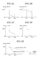
- FIGS. 3A to 3E show a combination of the frequency-controlled dimming and the duty ratio-controlled dimming, wherein a horizontal axis represents the switching frequency f, and a vertical axis represents the light output of the semiconductor light emitting element 3 .
- a dimming range is divided into a high luminance region and a low luminance region. Then, the duty ratio-controlled dimming is performed in the high luminance region and the frequency-controlled dimming is performed in the low luminance region. That is, from the full lighting state (state of FIG. 2A ) having a light output of 100%, while maintaining the switching frequency f at a minimum frequency fmin (e.g., about 45 kHz), the light output is reduced until the limit of dimming control using variation in the ratio of the ON periods of the switching elements Q 1 and Q 2 (e.g., state of FIG. 2B ).
- a minimum frequency fmin e.g., about 45 kHz
- the dimming is performed until the limit of dimming control using the frequency control (e.g., state of FIG. 2D ).
- a maximum frequency fmax e.g., about 83 kHz
- a dimming range is divided into a high luminance region and a low luminance region. Then, the frequency-controlled dimming is performed in the high luminance region and the duty ratio-controlled dimming is performed in the low luminance region. That is, from the full lighting state (state of FIG. 2A ) having an light output of 100%, by increasing the switching frequency f from the minimum frequency fmin (e.g., about 45 kHz) to the maximum frequency fmax (e.g., about 83 kHz) while maintaining the ON periods of the switching elements Q 1 and Q 2 to be substantially equal, the dimming is performed until the limit of dimming control using the frequency control (e.g., state of FIG. 2C ).
- the minimum frequency fmin e.g., about 45 kHz
- fmax e.g., about 83 kHz
- the light output is reduced until the limit of dimming control using the duty ratio control (e.g., state of FIG. 2D ).
- the duty ratio control e.g., state of FIG. 2D
- the current is distributed evenly to each switching element. Accordingly, it is possible to prevent excessive thermal stress from being applied to only one switching element.
- a control example of FIG. 3C is a compromise between the example of FIG. 3A and the example of FIG. 3B .
- a dimming range is divided into a high luminance region, a medium luminance region, and a low luminance region. Then, the duty ratio-controlled dimming is performed in the high luminance region and the low luminance region and the frequency-controlled dimming is performed in the medium luminance region.
- a control example of FIG. 3D is also a compromise between the example of FIG. 3A and the example of FIG. 3B .
- a dimming range is divided into a high luminance region, a medium luminance region, and a low luminance region. Then, the frequency-controlled dimming is performed in the high luminance region and the low luminance region and the duty ratio-controlled dimming is performed in the medium luminance region.
- a filter circuit for removing switching noise may be provided to selectively remove a frequency near the middle between the minimum frequency fmin and the maximum frequency fmax, so that it becomes possible to efficiently remove the switching noise in a luminance region with a relatively high use frequency.
- FIG. 3E A control example of FIG. 3E is an example in which the frequency-controlled dimming and the duty ratio-controlled dimming are performed at the same time.
- a solid line shows control characteristics of the present embodiment using a combination of the frequency-controlled dimming and the duty ratio-controlled dimming
- a dashed line shows control characteristics of the conventional case using only the frequency-controlled dimming.
- JP2001-351789 in case of extensively dimming the light output only by using the frequency control, it is necessary to expand a variation range of the frequency, and it is difficult to remove the switching noise.
- the resonant voltage is reduced due to an increase in switching frequency, and there is a problem in that it is difficult to obtain a voltage required for turning on the LED load. Further, there is a problem of an increase in switching loss.
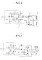
- FIG. 4 is a circuit diagram of a lighting device for a semiconductor light emitting element in accordance with a second embodiment of the present invention.
- the lighting device in this embodiment includes a DC input power source Vdc, power capacitors C 4 and C 5 , a bootstrap diode D 5 , signal sources V 1 and V 2 , resistors R 1 to R 5 , capacitors C 1 to C 3 , an inductor L 1 , an inverter circuit 1 and a rectifier circuit 2 .
- the signal sources V 1 and V 2 are respectively supplied with power from the power capacitors C 5 and C 4 .
- the power capacitor C 4 at the low potential side is charged from, e.g., the DC input power source Vdc through a resistor (not shown) with high resistance for step-down.
- the voltage across the power capacitor C 4 is regulated by a constant voltage element (not shown) such as a Zener diode, so that a substantially constant control power supply voltage Vcc is charged in the power capacitor C 4 .
- the power capacitor C 5 at the high potential side is charged from the power capacitor C 4 at the low potential side through the so-called bootstrap diode D 5 when the switching element Q 2 at the low potential side is turned on.
- the pulse width of the ON drive signal outputted from the signal source V 1 at the high potential side is controlled to be larger than the pulse width of the ON drive signal outputted from the signal source V 2 at the low potential side.
- the pulse width of the ON drive signal outputted from the signal source V 2 at the low potential side is controlled to be larger than the pulse width of the ON drive signal outputted from the signal source V 1 at the high potential side.
- the control power supply voltage HVcc at the high potential side will no longer be insufficient, even if an electrolytic capacitor with a relatively small capacitance is used as the power capacitor C 5 .
- an aluminum electrolytic capacitor used as the power capacitor easily loses its capacitance due to temperature rise or changes over time. For this reason, in the long-life LED lighting device, the electrolytic capacitor needs to be designed to have a large capacitance with a margin. In contrast, in the present embodiment, since the power capacitor C 5 at the high potential side can be designed to have a small capacitance, it is possible to achieve the miniaturization of the apparatus.
- FIG. 5 is a circuit diagram of a lighting device for a semiconductor light emitting element in accordance with a third embodiment of the present invention.
- the lighting device in this embodiment includes a DC input power source Vdc, signal sources V 1 and V 2 , resistors R 1 to R 6 , capacitors C 1 to C 3 , a capacitor C 6 , an inductor L 1 , switching elements Q 1 and Q 2 and diodes D 1 and D 3 .
- two half-wave rectifier circuits of opposite polarity formed of the diodes D 1 and D 3 , are connected in parallel in lieu of the full-wave rectifier circuit including the diodes D 1 to D 4 in the first embodiment shown in FIG. 1 .
- Connected to the resonant capacitor C 2 is a parallel circuit of a capacitor C 3 , a resistor R 5 and a semiconductor light emitting element 3 a through the diode D 1 .
- the semiconductor light emitting elements 3 a and 3 b may have the same color temperature, but may have different color temperatures (e.g., cold and warm colors). In the latter case, by controlling the ON periods of the switching elements Q 1 and Q 2 to be uneven, it is possible to vary the color temperature of mixed light. Further, the luminance of the mixed light may be adjusted by varying the switching frequency of the switching elements Q 1 and Q 2 , by intermittently setting a low frequency pause period in a high frequency switching operation, or by using both methods in combination.
- JP2001-351789 there has been proposed color mixing and dimming operation of semiconductor light emitting elements connected to the output of the half-bridge inverter circuit through the LC series resonant circuit (claim 6 in JP2001-351789).
- JP2001-351789 it is necessary to provide separate LC series resonant circuits having different resonant frequencies for the respective semiconductor light emitting elements having different color temperatures, which makes the circuit configuration complicated.
- the current flowing through the resonant circuit can be in the lagging mode all the time, it is possible to prevent two switching elements connected in series from being turned on at the same time, and to reduce switching loss. Further, since it can be configured by using only one LC series resonant circuit, there is an advantage of simple circuit configuration.
- the series circuit of the LED load may be connected in reverse parallel to both ends of the resonant capacitor C 2 .
- the diode characteristics of the LED also serve the function of the rectifier circuit 2 .
- the lighting device of each of the first to the third embodiments may be used in, e.g., a straight pipe type LED illumination apparatus 140 shown in FIG. 6 .
- FIG. 6 illustrates the straight pipe type LED illumination apparatus 140 in accordance with the fourth embodiment of the present invention.
- the straight pipe type LED illumination apparatus 140 shown in FIG. 6 is an illumination apparatus having one lamp.
- the LED illumination apparatus 140 includes an apparatus main body 141 in which the lighting device is installed, a pair of sockets 142 and 143 having lamp pin contact holes 145 through which the straight pipe type LED is attached to both ends of the apparatus main body 141 and a spring 144 , and a reflection plate 146 .
- each of the first to the third embodiments may be applied to an apparatus having two or more lamps.
- LEDs may be used instead of straight pipe type LEDs used in a shop or a facility.
- the light emitting diode has been illustrated as the semiconductor light emitting element, but it is not limited thereto.
- an organic electroluminescent (EL) element, semiconductor laser element or the like may be used.
Landscapes
- Circuit Arrangement For Electric Light Sources In General (AREA)
Abstract
Description
- The present invention relates to a lighting device for a semiconductor light emitting element such as a light emitting diode (LED) and an illumination apparatus including same.
- Japanese Patent Application Publication No. 2001-351789 (FIG. 1) (hereinafter referred to as JP2001-351789) discloses a technique of dimming an LED load by connecting the LED load to an output of a half-bridge inverter circuit via an LC series resonant circuit and varying a switching frequency.
- Japanese Patent No. 2,975,029 (FIG. 5) discloses a technique of dimming a discharge lamp load by connecting a hot cathode type discharge lamp load to an output of a half-bridge inverter circuit via an LC series resonant circuit and setting ON periods of two switching elements of the inverter circuit to be unequal during dimming. Further, there has been proposed a technique of supplying a preheating current while avoiding cold cathode discharge by setting the ON periods of the two switching elements of the inverter circuit to be substantially equal during preheating and setting a switching frequency to be sufficiently higher than a resonant frequency to reduce a resonant voltage applied to the load.
- In accordance with the technique of JP2001-351789, the dimming operation of the LED load is performed by varying the switching frequency. Thus, in order to widen a dimming range, it is necessary to expand a variation range of the switching frequency, and there is a problem in that a high frequency side switching loss increases, or it is difficult to design a filter circuit for removing a switching noise. Further, the LED load has diode type load characteristics in which the load current hardly flows therethrough when a voltage across the LED load is equal to or less than a predetermined load voltage. Accordingly, in case of increasing the switching frequency, the resonant voltage applied to the load is reduced, and there is problem in that it is impossible to obtain a voltage required for turning on the LED load.
- In JP2001-351789, there has also been proposed the technique of expanding the dimming range by intermittently pausing a high frequency switching operation at a low frequency (see Paragraph [0099] and FIG. 15 in JP2001-351789). However, in such case, there is a problem of an increase in flicker.
- In view of the above, the present invention provides a lighting device for a semiconductor light emitting element, capable of realizing a dimming operation in a wide range while limiting a range of a switching frequency.
- In accordance with an embodiment of the present invention, there is provided a lighting device for a semiconductor light emitting element, including: a series circuit of two switching elements which are alternately turned on, the series circuit being connected to a direct current (DC) input power source; and a reactance circuit connected between a connection node of the two switching elements and one end of the DC input power source through a capacitor, an output of the reactance circuit being supplied to the semiconductor light emitting element through a rectifier circuit. A dimming operation of the semiconductor light emitting element is performed by varying a ratio of ON periods of the two switching elements.
- In accordance with another embodiment of the present invention, there is provided a lighting device for a semiconductor light emitting element, including: a series circuit of two switching elements which are alternately turned on, the series circuit being connected to a direct current (DC) input power source; and a reactance circuit connected between a connection node of the switching elements and one end of the DC input power source through a capacitor, an output of the reactance circuit being supplied to the semiconductor light emitting element through a rectifier circuit. A dimming operation of the semiconductor light emitting element is performed by varying a switching frequency and a ratio of ON periods of the two switching elements.
- Further, the reactance circuit may include a series connection of a current-limiting choke and an additional capacitor, and the rectifier circuit may be connected to the additional capacitor.
- Further, each of the switching elements may be connected in parallel to an anti-parallel diode, and the switching frequency of the switching elements may be set to be higher than a series resonant frequency of the current-limiting choke and the additional capacitor.
- Further, the lighting device described above may further include a capacitor which is connected in parallel to the semiconductor light emitting element provided on an output side of the rectifier circuit.
- Further, the ON period of one of the switching elements at a low potential side of the DC input power source may be controlled to be longer than the ON period of the other one of the switching elements at a high potential side of the DC input power source, and the lighting device described above may further include a bootstrap diode through which a charging current flows to a power capacitor of a drive circuit of said the other one of the switching elements from a power capacitor of a drive circuit of said one of the switching elements when said one of the switching elements is turned on.
- Further, the rectifier circuit may include two half-wave rectifier circuits of reverse polarity, which are respectively connected to semiconductor light emitting elements having different color temperatures, and a color temperature of mixed light may be changed by controlling the ratio of the ON periods of the two switching elements, and luminance of the mixed light is changed by controlling the switching frequency of the two switching elements.
- In accordance with still another embodiment of the present invention, there is provided an illumination apparatus including the lighting device for the semiconductor light emitting element described above.
- In accordance with the present invention, a dimming operation of the semiconductor light emitting element is performed by varying a ratio of the ON periods of two switching elements that are alternately turned on. Thus, there is an effect of realizing the dimming operation in a wide range while limiting a range of the switching frequency.
- The objects and features of the present invention will become apparent from the following description of embodiments, given in conjunction with the accompanying drawings, in which:
-
FIG. 1 is a circuit diagram of a lighting device for a semiconductor light emitting element in accordance with a first embodiment of the present invention; -
FIGS. 2A to 2D are waveform diagrams of an operation of the lighting device of the first embodiment; -
FIGS. 3A to 3E are graphs showing the operation of the lighting device of the first embodiment; -
FIG. 4 is a circuit diagram of a lighting device for a semiconductor light emitting element in accordance with a second embodiment of the present invention; and -
FIG. 5 is a circuit diagram of a lighting device for a semiconductor light emitting element in accordance with a third embodiment of the present invention. -
FIG. 6 illustrates a configuration of an illumination apparatus in accordance with a fourth embodiment of the present invention. - Hereinafter, embodiments of the present invention will be described with reference to the accompanying drawings, which form a part hereof.
-
FIG. 1 is a circuit diagram of a lighting device for a semiconductor light emitting element in accordance with in accordance with a first embodiment of the present invention. - The
lighting device 10 in this embodiment includes a direct current (DC) input power source Vdc, signal sources V1 and V2, resistors R1 to R5, capacitors C1 to C3, an inductor L1, aninverter circuit 1 and arectifier circuit 2. - The direct current (DC) input power source Vdc supplies a substantially constant DC voltage of, e.g., about 420 V, which is converted from an alternating current (AC) voltage of a commercial AC power source via a filter circuit, a full-wave rectifier circuit and a step-up chopper circuit.
- The DC input power source Vdc is connected in parallel to a series circuit of two switching elements Q1 and Q2 which are alternately turned on, thereby forming the
inverter circuit 1. Each of the switching elements Q1 and Q2 is a power MOSFET capable of switching up to, e.g., about 500 V, 3 A, and has an anti-parallel diode therein. - Connected to both ends of the switching element Q2 is a series circuit of the inductor L1 and the capacitors C1 and C2. The capacitor C1 is set to have a sufficiently large capacitance compared to the capacitor C2. For example, the capacitance of the capacitor C2 is as small as about 0.011 μF, whereas the capacitance of the capacitor C1 is set to be as large as about 0.22 μF. In this case, the capacitor C1 substantially functions as a capacitor for cutting a DC component, whereas the capacitor C2 functions as a resonant capacitor across which a voltage oscillates at a high frequency.
- The inductor L1 is a current-limiting choke of about 1.7 mH. The inductor L1 and the capacitor C2 constitute an LC series resonant circuit (reactance circuit). A resonant frequency under no-load condition, i.e., a resonant frequency of the inductor L1 and the capacitor C2 without load, is fo=1/(2π√{square root over ((L1·C2))})≈37 kHz. An operating frequency of ON/OFF of the switching elements Q1 and Q2 is set to be higher than the resonant frequency fo.
- Accordingly, the current flowing through the switching elements Q1 and Q2 is in a so-called lagging mode, so that there is a period in which when one of the switching elements is turned off, the current flows through the other switching element in a backward direction. After the end of this period, the current flows through the other switching element in a forward direction.
- Therefore, in this embodiment, an ON period of one switching element is a drive period in which the switching element is driven on in the forward direction. In an initial part of the ON period, current flows in the reverse direction through an anti-parallel diode connected to that switching element. In the remaining part of the ON period, current flows through the switching element in the forward direction. Further, the switching element is forcibly turned off by cutting off an ON drive signal while the current flows in the forward direction, so that a flyback current flows through an anti-parallel diode of the other switching element.
- The switching elements Q1 and Q2 are respectively controlled by a square wave voltage signal (ON drive signal) supplied from the signal sources (drive circuits of the switching elements Q1 and Q2) V1 and V2. The ON drive signal of the switching element Q1 is supplied from the signal source V1 through the resistors R1 and R2. The ON drive signal of the switching element Q2 is supplied from the signal source V2 through the resistors R3 and R4. Each of the resistors R1 and R3 has a low resistance of about 10Ω, and each of the resistors R2 and R4 has a high resistance of about 10 Ω.
- The signal sources V1 and V2 operate in conjunction with each other to output ON drive signals as shown in
FIGS. 2A to 2D based on the dimming level. The amplitude of the ON drive signal is set to be higher than a threshold voltage between gate and source of each of the switching elements Q1 and Q2, and is, e.g., about 15 V. -
FIGS. 2A to 2D are waveform diagrams of an operation of the lighting device of the first embodiment. Specifically,FIG. 2A is a waveform diagram of the ON drive signals in a full lighting state. In this example, the pulse width of both the ON drive signals from the signal sources V1 and V2 is 10.5 μs, and a dead-off time of 0.5 μs is inserted between the ON drive signals. Since one period of switching is 22 μs, a switching frequency is about 45 kHz. This is slightly higher than the resonant frequency fo (1/(2π√{square root over ((L1·C2))})≈37 kHz) of the inductor L1 and the capacitor C2 without load. Thus, a resonant current flows in the lagging mode. - By this resonant current, a high frequency voltage alternating at the switching frequency is generated across the capacitor C2 with a small capacitance. However, in the capacitor C1 with a large capacitance, a DC voltage is charged such that the side of the inductor L1 is a positive electrode and the side of the capacitor C2 is a negative electrode. The DC voltage charged in the capacitor C1 becomes approximately half of the DC voltage from the DC input power source Vdc if the switching elements Q1 and Q2 have the same ON period.
- The high frequency voltage generated across the capacitor C2 is full-wave rectified by the full-
wave rectifier circuit 2 including diodes D1 to D4, so that a DC voltage is generated in a parallel circuit of the capacitor C3 and the resistor R5. A semiconductorlight emitting element 3 is connected in parallel to the parallel circuit of the capacitor C3 and the resistor R5. The capacitor C3 includes two capacitors of, e.g., about 0.82 μF which are connected in parallel. The resistor R5 has a resistance value of about 100Ω. The semiconductorlight emitting element 3 is a circuit including, e.g., twenty-four LEDs connected in series, and is turned on by a DC voltage of the capacitor C3. In the example ofFIG. 2A , a load current flowing through the semiconductorlight emitting element 3 was about 300 mA. Further, a load voltage was about 73 V. - Next, in an example of
FIG. 2B , the pulse width of the ON drive signal of the switching element Q1 outputted from the signal source V1 is 20 μs, whereas the pulse width of the ON drive signal of the switching element Q2 outputted from the signal source V2 is 1 μs, and a dead-off time of 0.5 μs is inserted between the ON drive signals. Since one period of switching is 22 μs, a switching frequency is about 45 kHz as in the example ofFIG. 2A . However, since a ratio of the ON period of the switching element Q1 to the ON period of the switching element Q2 is 20:1 and the ON periods are uneven, the DC voltage across the capacitor C1 for cutting a DC component is higher than approximately half of the DC voltage from the DC input power source Vdc. In this case, as disclosed in Japanese Patent No. 2,975,029, the current supplied to the load connected to the capacitor C2 is reduced. In the example ofFIG. 2B , the present inventors have found that the load current flowing through the semiconductorlight emitting element 3 was about 40 mA. - In an example of
FIG. 2C , the pulse width of both the ON drive signals from the signal sources V1 and V2 is 5.5 μs, and a dead-off time of 0.5 μs is inserted between the On drive signals. Since one period of switching is 12 μs, a switching frequency is about 83 kHz. This is largely higher than the resonant frequency fo (1/(2π√{square root over ((L1·C2))})≈37 kHz) at which only the inductor L1 and the capacitor C2 are present without load. Thus, the voltage across the resonant capacitor C2 is reduced, and the load current flowing through the semiconductorlight emitting element 3 was about 13 mA. - In an example of
FIG. 2D , the pulse width of the ON drive signal of the switching element Q1 outputted from the signal source V1 is 10 μs, whereas the pulse width of the ON drive signal of the switching element Q2 outputted from the signal source V2 is 1 μs, and a dead-off time of 0.5 μs is inserted between the ON drive signals. Since one period of switching is 12 μs, a switching frequency is about 83 kHz as in the example ofFIG. 2C . This is largely higher than the resonant frequency fo (1/(2π√{square root over ((L1·C2))})≈37 kHz) at which only the inductor L1 and the capacitor C2 are present without load. - Further, a ratio of the ON period of the switching element Q1 to the ON period of the switching element Q2 is 10:1, and the DC voltage across the capacitor C1 for cutting a DC component is higher than approximately half of the DC voltage from the DC input power source Vdc. In this case, since the frequency-controlled dimming as in the example of
FIG. 2C and the duty ratio-controlled dimming as in the example ofFIG. 2B are performed at the same time, by its synergistic effect, the load current flowing through the semiconductorlight emitting element 3 is significantly reduced, and was about 1.25 mA. - As described above, in a minimum dimming state (load current: about 1.25 mA) of
FIG. 2D , it is possible to realize dimming in a wide range of 240:1 compared to the full lighting state (load current: about 300 mA) ofFIG. 2A . On the other hand, in the minimum dimming state (frequency: about 83 kHz) ofFIG. 2D , a variation range of the switching frequency can be limited to a narrow range less than twice the frequency of the full lighting state (frequency: about 45 kHz) ofFIG. 2A . - Therefore, in accordance with the embodiment of the present invention, there is an advantage that it is possible to realize dimming control in a wide range while maintaining a narrow variation range of the switching frequency.
- Further, in the examples of
FIGS. 2A to 2D , the dead-off time is inserted in order to eliminate a period in which the switching elements Q1 and Q2 are turned on at the same time, and is not limited to 0.5 μs. The same is true for other numbers. -
FIGS. 3A to 3E show a combination of the frequency-controlled dimming and the duty ratio-controlled dimming, wherein a horizontal axis represents the switching frequency f, and a vertical axis represents the light output of the semiconductorlight emitting element 3. - In a control example of
FIG. 3A , a dimming range is divided into a high luminance region and a low luminance region. Then, the duty ratio-controlled dimming is performed in the high luminance region and the frequency-controlled dimming is performed in the low luminance region. That is, from the full lighting state (state ofFIG. 2A ) having a light output of 100%, while maintaining the switching frequency f at a minimum frequency fmin (e.g., about 45 kHz), the light output is reduced until the limit of dimming control using variation in the ratio of the ON periods of the switching elements Q1 and Q2 (e.g., state ofFIG. 2B ). - After that, by increasing the switching frequency f up to a maximum frequency fmax (e.g., about 83 kHz), the dimming is performed until the limit of dimming control using the frequency control (e.g., state of
FIG. 2D ). In this case, it is possible to reduce the number of times of switching in the high luminance region in which the switching current is high, so that the switching loss can be reduced while reducing the switching noise. - In a control example of
FIG. 3B , a dimming range is divided into a high luminance region and a low luminance region. Then, the frequency-controlled dimming is performed in the high luminance region and the duty ratio-controlled dimming is performed in the low luminance region. That is, from the full lighting state (state ofFIG. 2A ) having an light output of 100%, by increasing the switching frequency f from the minimum frequency fmin (e.g., about 45 kHz) to the maximum frequency fmax (e.g., about 83 kHz) while maintaining the ON periods of the switching elements Q1 and Q2 to be substantially equal, the dimming is performed until the limit of dimming control using the frequency control (e.g., state ofFIG. 2C ). - After that, by controlling the ON periods of the switching elements Q1 and Q2 to be uneven, the light output is reduced until the limit of dimming control using the duty ratio control (e.g., state of
FIG. 2D ). In this case, in the high luminance region in which the switching current is high, the current is distributed evenly to each switching element. Accordingly, it is possible to prevent excessive thermal stress from being applied to only one switching element. - A control example of
FIG. 3C is a compromise between the example ofFIG. 3A and the example ofFIG. 3B . In this case, a dimming range is divided into a high luminance region, a medium luminance region, and a low luminance region. Then, the duty ratio-controlled dimming is performed in the high luminance region and the low luminance region and the frequency-controlled dimming is performed in the medium luminance region. - In this case, as in the control example of
FIG. 3A , since it is possible to reduce the number of times of switching in the high luminance region in which the switching current is high, there is an advantage that it is possible to reduce the switching loss while reducing the switching noise. Further, since the frequency-controlled dimming is started before the ON periods of the switching elements Q1 and Q2 become excessively uneven, it is possible to reduce the imbalance of thermal stress of each switching element. - A control example of
FIG. 3D is also a compromise between the example ofFIG. 3A and the example ofFIG. 3B . In this case, a dimming range is divided into a high luminance region, a medium luminance region, and a low luminance region. Then, the frequency-controlled dimming is performed in the high luminance region and the low luminance region and the duty ratio-controlled dimming is performed in the medium luminance region. For example, if frequency of use is low in the vicinity of a maximum output or minimum output, a filter circuit for removing switching noise may be provided to selectively remove a frequency near the middle between the minimum frequency fmin and the maximum frequency fmax, so that it becomes possible to efficiently remove the switching noise in a luminance region with a relatively high use frequency. - A control example of
FIG. 3E is an example in which the frequency-controlled dimming and the duty ratio-controlled dimming are performed at the same time. InFIG. 3 , a solid line shows control characteristics of the present embodiment using a combination of the frequency-controlled dimming and the duty ratio-controlled dimming, and a dashed line shows control characteristics of the conventional case using only the frequency-controlled dimming. As in the conventional case (JP2001-351789), in case of extensively dimming the light output only by using the frequency control, it is necessary to expand a variation range of the frequency, and it is difficult to remove the switching noise. Further, particularly, in the low luminance region, the resonant voltage is reduced due to an increase in switching frequency, and there is a problem in that it is difficult to obtain a voltage required for turning on the LED load. Further, there is a problem of an increase in switching loss. - In contrast, in the control characteristics (solid line) of the present embodiment using a combination of the frequency-controlled dimming and the duty ratio-controlled dimming, even if the variation range of the frequency is narrow, it is possible to realize dimming operation in a wide range by performing the duty ratio control in combination with the frequency control. Accordingly, it is possible to easily design the filter circuit for removing switching noise, and it is possible to avoid an increase in switching loss. Further, since it is possible to prevent the resonant voltage from being reduced due to an excessive increase in switching frequency, it is possible to realize an LED illumination apparatus capable of performing stable dimming operation even at a low light flux without causing a problem such that it is impossible to obtain a voltage required for turning on the LED load.
-
FIG. 4 is a circuit diagram of a lighting device for a semiconductor light emitting element in accordance with a second embodiment of the present invention. The lighting device in this embodiment includes a DC input power source Vdc, power capacitors C4 and C5, a bootstrap diode D5, signal sources V1 and V2, resistors R1 to R5, capacitors C1 to C3, an inductor L1, aninverter circuit 1 and arectifier circuit 2. - The signal sources V1 and V2 are respectively supplied with power from the power capacitors C5 and C4. The power capacitor C4 at the low potential side is charged from, e.g., the DC input power source Vdc through a resistor (not shown) with high resistance for step-down. The voltage across the power capacitor C4 is regulated by a constant voltage element (not shown) such as a Zener diode, so that a substantially constant control power supply voltage Vcc is charged in the power capacitor C4. The power capacitor C5 at the high potential side is charged from the power capacitor C4 at the low potential side through the so-called bootstrap diode D5 when the switching element Q2 at the low potential side is turned on.
- In the first embodiment, when the ON drive signals of the switching elements Q1 and Q2 are controlled to be uneven, as shown in
FIG. 2B or 2D, the pulse width of the ON drive signal outputted from the signal source V1 at the high potential side is controlled to be larger than the pulse width of the ON drive signal outputted from the signal source V2 at the low potential side. On the other hand, in the second embodiment, when the ON drive signals of the switching elements Q1 and Q2 are controlled to be uneven, the pulse width of the ON drive signal outputted from the signal source V2 at the low potential side is controlled to be larger than the pulse width of the ON drive signal outputted from the signal source V1 at the high potential side. Accordingly, since the charging time of the power capacitor C5 at the high potential side is not shorter than the discharging time thereof, the control power supply voltage HVcc at the high potential side will no longer be insufficient, even if an electrolytic capacitor with a relatively small capacitance is used as the power capacitor C5. - As known, an aluminum electrolytic capacitor used as the power capacitor easily loses its capacitance due to temperature rise or changes over time. For this reason, in the long-life LED lighting device, the electrolytic capacitor needs to be designed to have a large capacitance with a margin. In contrast, in the present embodiment, since the power capacitor C5 at the high potential side can be designed to have a small capacitance, it is possible to achieve the miniaturization of the apparatus.
-
FIG. 5 is a circuit diagram of a lighting device for a semiconductor light emitting element in accordance with a third embodiment of the present invention. The lighting device in this embodiment includes a DC input power source Vdc, signal sources V1 and V2, resistors R1 to R6, capacitors C1 to C3, a capacitor C6, an inductor L1, switching elements Q1 and Q2 and diodes D1 and D3. - In this embodiment, two half-wave rectifier circuits of opposite polarity, formed of the diodes D1 and D3, are connected in parallel in lieu of the full-wave rectifier circuit including the diodes D1 to D4 in the first embodiment shown in
FIG. 1 . Connected to the resonant capacitor C2 is a parallel circuit of a capacitor C3, a resistor R5 and a semiconductorlight emitting element 3 a through the diode D1. Further, connected to the resonant capacitor C2 is a parallel circuit of a capacitor C6, a resistor R6 and a semiconductorlight emitting element 3 b through the diode D3 of reverse polarity. - The semiconductor
light emitting elements - In the above-mentioned JP2001-351789, there has been proposed color mixing and dimming operation of semiconductor light emitting elements connected to the output of the half-bridge inverter circuit through the LC series resonant circuit (claim 6 in JP2001-351789). However, in the technique of JP2001-351789, it is necessary to provide separate LC series resonant circuits having different resonant frequencies for the respective semiconductor light emitting elements having different color temperatures, which makes the circuit configuration complicated. Further, in order to vary the color temperature of the mixed light, it is necessary to change the switching between the different resonant frequencies, and the current flowing through one of the resonant circuits is in a leading mode (
claim 3 in JP2001-351789). - On the other hand, in accordance with the configuration of the present embodiment, since the current flowing through the resonant circuit can be in the lagging mode all the time, it is possible to prevent two switching elements connected in series from being turned on at the same time, and to reduce switching loss. Further, since it can be configured by using only one LC series resonant circuit, there is an advantage of simple circuit configuration.
- Further, in accordance with the configuration of the present embodiment, it is possible to control the color temperature of the mixed light by changing the ratio of the ON periods of two switching elements, and also it is possible to control the luminance of the mixed light by changing the switching frequency. Accordingly, compared to the control of varying the color temperature of the mixed light by changing the switching frequency as in the technique of JP2001-351789, it is no longer required to set a pause period of the switching operation for dimming control (see Paragraph [0099] and FIG. 15 in JP2001-351789). Thus, compared to the technique of JP2001-351789, it is possible to reduce the flicker.
- In addition, although not shown, as in JP2001-351789, the series circuit of the LED load may be connected in reverse parallel to both ends of the resonant capacitor C2. In such case, the diode characteristics of the LED also serve the function of the
rectifier circuit 2. - The lighting device of each of the first to the third embodiments may be used in, e.g., a straight pipe type
LED illumination apparatus 140 shown inFIG. 6 .FIG. 6 illustrates the straight pipe typeLED illumination apparatus 140 in accordance with the fourth embodiment of the present invention. The straight pipe typeLED illumination apparatus 140 shown inFIG. 6 is an illumination apparatus having one lamp. - As illustrated in
FIG. 6 , theLED illumination apparatus 140 includes an apparatusmain body 141 in which the lighting device is installed, a pair ofsockets main body 141 and aspring 144, and areflection plate 146. - When the lighting device of each of the first to the third embodiments is applied to the
illumination apparatus 140 shown inFIG. 6 , the same effect as that of the above embodiment can be obtained. - Further, the lighting device of each of the first to the third embodiments may be applied to an apparatus having two or more lamps.
- Further, various shapes of LEDs may be used instead of straight pipe type LEDs used in a shop or a facility.
- In the above embodiments, the light emitting diode has been illustrated as the semiconductor light emitting element, but it is not limited thereto. For example, an organic electroluminescent (EL) element, semiconductor laser element or the like may be used.
- While the invention has been shown and described with respect to the embodiments, it will be understood by those skilled in the art that various changes and modification may be made without departing from the scope of the invention as defined in the following claims.
Claims (14)
Applications Claiming Priority (2)
| Application Number | Priority Date | Filing Date | Title |
|---|---|---|---|
| JP2011083185A JP5828067B2 (en) | 2011-04-04 | 2011-04-04 | Semiconductor light-emitting element lighting device and lighting fixture using the same |
| JP2011-083185 | 2011-04-04 |
Publications (2)
| Publication Number | Publication Date |
|---|---|
| US20120249003A1 true US20120249003A1 (en) | 2012-10-04 |
| US8896221B2 US8896221B2 (en) | 2014-11-25 |
Family
ID=46926299
Family Applications (1)
| Application Number | Title | Priority Date | Filing Date |
|---|---|---|---|
| US13/433,406 Expired - Fee Related US8896221B2 (en) | 2011-04-04 | 2012-03-29 | Lighting device for semiconductor light emitting element and illumination apparatus including same |
Country Status (3)
| Country | Link |
|---|---|
| US (1) | US8896221B2 (en) |
| JP (1) | JP5828067B2 (en) |
| CN (1) | CN102740547B (en) |
Cited By (8)
| Publication number | Priority date | Publication date | Assignee | Title |
|---|---|---|---|---|
| CN103906311A (en) * | 2012-12-27 | 2014-07-02 | 日立空调·家用电器株式会社 | Lighting device |
| WO2014188219A1 (en) * | 2013-05-23 | 2014-11-27 | Led Lighting Consultants Limited | Improvements relating to power adaptors |
| US20150097493A1 (en) * | 2012-05-25 | 2015-04-09 | Osram Gmbh | Load driver and luminaire including the load driver |
| US9313844B2 (en) | 2014-09-10 | 2016-04-12 | Panasonic Intellectual Property Management Co., Ltd. | Lighting device and luminaire |
| US9549442B1 (en) | 2015-06-26 | 2017-01-17 | Samsung Electronics Co., Ltd. | Light emitting device (LED) driving apparatus and lighting device including the same |
| US9723666B2 (en) | 2015-01-06 | 2017-08-01 | Panasonic Intellectual Property Management Co., Ltd. | Lighting device and lighting fixture using same |
| WO2017186968A1 (en) * | 2016-04-29 | 2017-11-02 | Tridonic Gmbh & Co Kg | Method for controlling an led module |
| DE102018001852A1 (en) | 2017-03-24 | 2018-09-27 | SEW-EURODRlVE GmbH & Co. KG | A system comprising a connector part and a corresponding mating connector part for forming a connector, and method of operating a system |
Families Citing this family (8)
| Publication number | Priority date | Publication date | Assignee | Title |
|---|---|---|---|---|
| JP6231133B2 (en) * | 2013-01-25 | 2017-11-15 | フィリップス ライティング ホールディング ビー ヴィ | Lighting device and lighting system |
| KR101454697B1 (en) * | 2013-02-20 | 2014-10-27 | 서강대학교산학협력단 | Motion Sensor Driven Automatic LED Lighting Devices |
| CN104080235B (en) * | 2013-03-28 | 2017-03-15 | 赛尔富电子有限公司 | A kind of LED lamp regulator control system |
| CN104080236B (en) * | 2013-03-28 | 2017-03-15 | 赛尔富电子有限公司 | A kind of LED lamp regulator control system |
| KR101504279B1 (en) | 2013-06-12 | 2015-03-20 | 주식회사 파이텍 | Drive circuit of Light-Emitting Diode |
| GB201322022D0 (en) * | 2013-12-12 | 2014-01-29 | Led Lighting Consultants Ltd | Improvements relating to power adaptors |
| US9968129B2 (en) * | 2015-07-31 | 2018-05-15 | R.J. Reynolds Tobacco Company | Product and package including power producer and output mechanism, and related method |
| JP2019204710A (en) * | 2018-05-24 | 2019-11-28 | パナソニックIpマネジメント株式会社 | Led lighting device and lighting fixture |
Citations (4)
| Publication number | Priority date | Publication date | Assignee | Title |
|---|---|---|---|---|
| US5434479A (en) * | 1992-09-22 | 1995-07-18 | Matsushita Electric Works, Ltd. | Full-bridge inverter for discharge lamp lighting device with varied transistor zero voltage period |
| US20030043611A1 (en) * | 2000-03-17 | 2003-03-06 | Tridonicatco Gmbh & Co. Kg | Drive for light-emitting diodes |
| US20090021175A1 (en) * | 2006-03-06 | 2009-01-22 | Koninklijke Philips Electronics N.V. | Supply circuit and device comprising a supply circuit |
| US20090295300A1 (en) * | 2008-02-08 | 2009-12-03 | Purespectrum, Inc | Methods and apparatus for a dimmable ballast for use with led based light sources |
Family Cites Families (7)
| Publication number | Priority date | Publication date | Assignee | Title |
|---|---|---|---|---|
| JP2975029B2 (en) | 1989-08-28 | 1999-11-10 | 松下電工株式会社 | Discharge lamp lighting device |
| JP3736096B2 (en) * | 1997-06-12 | 2006-01-18 | 株式会社日立製作所 | Lighting device and lamp using the same |
| JP2001351789A (en) | 2000-06-02 | 2001-12-21 | Toshiba Lighting & Technology Corp | LED driver |
| JP2008171984A (en) * | 2007-01-11 | 2008-07-24 | Showa Denko Kk | Light-emitting device and drive method thereof |
| JP2010086943A (en) * | 2008-09-04 | 2010-04-15 | Toshiba Lighting & Technology Corp | Led lighting device and illumination fixture |
| CN201374865Y (en) * | 2009-03-11 | 2009-12-30 | 冠捷投资有限公司 | Inverter control circuit |
| JP5070263B2 (en) * | 2009-09-11 | 2012-11-07 | 三菱電機株式会社 | LED lighting device and lighting device |
-
2011
- 2011-04-04 JP JP2011083185A patent/JP5828067B2/en active Active
-
2012
- 2012-03-29 CN CN201210088454.XA patent/CN102740547B/en not_active Expired - Fee Related
- 2012-03-29 US US13/433,406 patent/US8896221B2/en not_active Expired - Fee Related
Patent Citations (4)
| Publication number | Priority date | Publication date | Assignee | Title |
|---|---|---|---|---|
| US5434479A (en) * | 1992-09-22 | 1995-07-18 | Matsushita Electric Works, Ltd. | Full-bridge inverter for discharge lamp lighting device with varied transistor zero voltage period |
| US20030043611A1 (en) * | 2000-03-17 | 2003-03-06 | Tridonicatco Gmbh & Co. Kg | Drive for light-emitting diodes |
| US20090021175A1 (en) * | 2006-03-06 | 2009-01-22 | Koninklijke Philips Electronics N.V. | Supply circuit and device comprising a supply circuit |
| US20090295300A1 (en) * | 2008-02-08 | 2009-12-03 | Purespectrum, Inc | Methods and apparatus for a dimmable ballast for use with led based light sources |
Cited By (11)
| Publication number | Priority date | Publication date | Assignee | Title |
|---|---|---|---|---|
| US20150097493A1 (en) * | 2012-05-25 | 2015-04-09 | Osram Gmbh | Load driver and luminaire including the load driver |
| US9356532B2 (en) * | 2012-05-25 | 2016-05-31 | Osram Gmbh | Load driver and luminaire including the load driver |
| CN103906311A (en) * | 2012-12-27 | 2014-07-02 | 日立空调·家用电器株式会社 | Lighting device |
| WO2014188219A1 (en) * | 2013-05-23 | 2014-11-27 | Led Lighting Consultants Limited | Improvements relating to power adaptors |
| US20160126860A1 (en) * | 2013-05-23 | 2016-05-05 | Led Lighting Consultants Limited | Improvements relating to power adaptors |
| US10790762B2 (en) * | 2013-05-23 | 2020-09-29 | Adp Corporate Limited | Relating to power adaptors |
| US9313844B2 (en) | 2014-09-10 | 2016-04-12 | Panasonic Intellectual Property Management Co., Ltd. | Lighting device and luminaire |
| US9723666B2 (en) | 2015-01-06 | 2017-08-01 | Panasonic Intellectual Property Management Co., Ltd. | Lighting device and lighting fixture using same |
| US9549442B1 (en) | 2015-06-26 | 2017-01-17 | Samsung Electronics Co., Ltd. | Light emitting device (LED) driving apparatus and lighting device including the same |
| WO2017186968A1 (en) * | 2016-04-29 | 2017-11-02 | Tridonic Gmbh & Co Kg | Method for controlling an led module |
| DE102018001852A1 (en) | 2017-03-24 | 2018-09-27 | SEW-EURODRlVE GmbH & Co. KG | A system comprising a connector part and a corresponding mating connector part for forming a connector, and method of operating a system |
Also Published As
| Publication number | Publication date |
|---|---|
| JP2012221599A (en) | 2012-11-12 |
| CN102740547B (en) | 2014-08-13 |
| US8896221B2 (en) | 2014-11-25 |
| JP5828067B2 (en) | 2015-12-02 |
| CN102740547A (en) | 2012-10-17 |
Similar Documents
| Publication | Publication Date | Title |
|---|---|---|
| US8896221B2 (en) | Lighting device for semiconductor light emitting element and illumination apparatus including same | |
| EP2503845B1 (en) | Lighting device for solid-state light source, and illumination apparatus and system including same | |
| US9220159B2 (en) | Electronic ballast | |
| TWI420972B (en) | Circuits for driving light source, methods for controlling dimming of light source, driving systems, and controllers for regulating brightness of light source | |
| JP6031669B2 (en) | Circuit device for operating a low-power illumination unit and method for operating the same | |
| KR101001241B1 (en) | AC LED dimmer and dimming method | |
| EP2653011B1 (en) | Linear driver for reduced perceived light flicker | |
| JP6072776B2 (en) | LED retrofit drive circuit and method for operating LED retrofit drive circuit | |
| US9531255B2 (en) | Low-cost driver circuit with improved power factor | |
| JP5507957B2 (en) | Power circuit | |
| JP5562081B2 (en) | LED dimming method and dimming device | |
| KR101029874B1 (en) | Ac led dimmer and dimming method thereby | |
| KR101367383B1 (en) | Ac led dimmer | |
| JP2009026466A (en) | Lighting control circuit | |
| EP3081054B1 (en) | Improvements relating to power adaptors | |
| WO2013035177A1 (en) | Dimming method and dimming device for led | |
| KR101439899B1 (en) | Led lighting control apparatus | |
| KR20150125404A (en) | An lighting device |
Legal Events
| Date | Code | Title | Description |
|---|---|---|---|
| AS | Assignment |
Owner name: PANASONIC CORPORATION, JAPAN Free format text: ASSIGNMENT OF ASSIGNORS INTEREST;ASSIGNORS:ESAKI, SANA;HIRAMATU, AKINORI;REEL/FRAME:029283/0797 Effective date: 20120227 |
|
| STCF | Information on status: patent grant |
Free format text: PATENTED CASE |
|
| MAFP | Maintenance fee payment |
Free format text: PAYMENT OF MAINTENANCE FEE, 4TH YEAR, LARGE ENTITY (ORIGINAL EVENT CODE: M1551) Year of fee payment: 4 |
|
| FEPP | Fee payment procedure |
Free format text: MAINTENANCE FEE REMINDER MAILED (ORIGINAL EVENT CODE: REM.); ENTITY STATUS OF PATENT OWNER: LARGE ENTITY |
|
| LAPS | Lapse for failure to pay maintenance fees |
Free format text: PATENT EXPIRED FOR FAILURE TO PAY MAINTENANCE FEES (ORIGINAL EVENT CODE: EXP.); ENTITY STATUS OF PATENT OWNER: LARGE ENTITY |
|
| STCH | Information on status: patent discontinuation |
Free format text: PATENT EXPIRED DUE TO NONPAYMENT OF MAINTENANCE FEES UNDER 37 CFR 1.362 |
|
| FP | Lapsed due to failure to pay maintenance fee |
Effective date: 20221125 |