US20110080191A1 - System and Method for Clock-Synchronized Triangular Waveform Generation - Google Patents
System and Method for Clock-Synchronized Triangular Waveform Generation Download PDFInfo
- Publication number
- US20110080191A1 US20110080191A1 US12/574,663 US57466309A US2011080191A1 US 20110080191 A1 US20110080191 A1 US 20110080191A1 US 57466309 A US57466309 A US 57466309A US 2011080191 A1 US2011080191 A1 US 2011080191A1
- Authority
- US
- United States
- Prior art keywords
- clock signal
- triangular waveform
- voltage
- calibration
- signal
- Prior art date
- Legal status (The legal status is an assumption and is not a legal conclusion. Google has not performed a legal analysis and makes no representation as to the accuracy of the status listed.)
- Granted
Links
- 238000000034 method Methods 0.000 title claims description 26
- 230000001360 synchronised effect Effects 0.000 claims abstract description 26
- 230000000630 rising effect Effects 0.000 claims description 26
- 239000003990 capacitor Substances 0.000 claims description 22
- 230000000295 complement effect Effects 0.000 claims description 9
- 238000007670 refining Methods 0.000 claims 3
- 230000008014 freezing Effects 0.000 claims 2
- 238000007710 freezing Methods 0.000 claims 2
- 230000008569 process Effects 0.000 description 16
- 239000010752 BS 2869 Class D Substances 0.000 description 9
- 230000008901 benefit Effects 0.000 description 4
- 238000010586 diagram Methods 0.000 description 4
- 230000011664 signaling Effects 0.000 description 4
- 238000007599 discharging Methods 0.000 description 3
- 230000000694 effects Effects 0.000 description 3
- 238000012986 modification Methods 0.000 description 3
- 230000004048 modification Effects 0.000 description 3
- 238000013461 design Methods 0.000 description 2
- 238000005070 sampling Methods 0.000 description 2
- 238000004088 simulation Methods 0.000 description 2
- 101100113692 Caenorhabditis elegans clk-2 gene Proteins 0.000 description 1
- 230000008859 change Effects 0.000 description 1
- 238000004891 communication Methods 0.000 description 1
- 230000001276 controlling effect Effects 0.000 description 1
- 238000012937 correction Methods 0.000 description 1
- 230000002596 correlated effect Effects 0.000 description 1
- 230000000875 corresponding effect Effects 0.000 description 1
- 230000003247 decreasing effect Effects 0.000 description 1
- 230000008713 feedback mechanism Effects 0.000 description 1
- 238000004806 packaging method and process Methods 0.000 description 1
- 230000010363 phase shift Effects 0.000 description 1
- 230000003252 repetitive effect Effects 0.000 description 1
- 239000004065 semiconductor Substances 0.000 description 1
- 239000007787 solid Substances 0.000 description 1
- 230000005236 sound signal Effects 0.000 description 1
- 230000003595 spectral effect Effects 0.000 description 1
- 230000007704 transition Effects 0.000 description 1
Images


Classifications
-
- H—ELECTRICITY
- H03—ELECTRONIC CIRCUITRY
- H03F—AMPLIFIERS
- H03F3/00—Amplifiers with only discharge tubes or only semiconductor devices as amplifying elements
- H03F3/20—Power amplifiers, e.g. Class B amplifiers, Class C amplifiers
- H03F3/21—Power amplifiers, e.g. Class B amplifiers, Class C amplifiers with semiconductor devices only
- H03F3/217—Class D power amplifiers; Switching amplifiers
-
- H—ELECTRICITY
- H03—ELECTRONIC CIRCUITRY
- H03K—PULSE TECHNIQUE
- H03K4/00—Generating pulses having essentially a finite slope or stepped portions
- H03K4/06—Generating pulses having essentially a finite slope or stepped portions having triangular shape
-
- H—ELECTRICITY
- H03—ELECTRONIC CIRCUITRY
- H03K—PULSE TECHNIQUE
- H03K4/00—Generating pulses having essentially a finite slope or stepped portions
- H03K4/06—Generating pulses having essentially a finite slope or stepped portions having triangular shape
- H03K4/08—Generating pulses having essentially a finite slope or stepped portions having triangular shape having sawtooth shape
- H03K4/48—Generating pulses having essentially a finite slope or stepped portions having triangular shape having sawtooth shape using as active elements semiconductor devices
- H03K4/50—Generating pulses having essentially a finite slope or stepped portions having triangular shape having sawtooth shape using as active elements semiconductor devices in which a sawtooth voltage is produced across a capacitor
Definitions
- the present invention relates generally to pulse width modulation (PWM) and class-D amplifiers and specifically to clock-synchronized triangular waveform generators.
- PWM pulse width modulation
- class-D amplifiers specifically to clock-synchronized triangular waveform generators.
- PWM pulse-width modulation
- the class-D amplifier produces an output comprising a sequence of pulses.
- Pulse-width modulation is typically employed to encode audio information into these pulses by varying their individual widths.
- the average value of these pulses represents the instantaneous amplitude of the output signal.
- These pulses also introduce unwanted high-frequency content which may be removed by a low pass filter.
- FIG. 1 is a block diagram illustrating the typical architecture of a class-D amplifier 100 .
- the input signal is converted to pulses using modulator 102 which can be a pulse-width modulator.
- modulator 102 can be a pulse-width modulator.
- a common implementation of a pulse-width modulator uses a high-speed comparator to compare the input signal against a triangle wave.
- the modulated signal is then amplified by amplifier 104 and finally demodulated by low pass filter 106 .
- the demodulated signal can then be used, for example by speaker 108 .
- FIG. 2 shows a typical PWM generator.
- Input reference signal 202 is compared by comparator 206 against a repetitive modulation source, such as a sawtooth or triangular waveform generated by ramp generator 204 .
- a repetitive modulation source such as a sawtooth or triangular waveform generated by ramp generator 204 .
- the signal level of PWM output signal 208 is high; when the input reference signal is less than the modulation source, the signal level of PWM output signal 208 is low.
- FIG. 3A shows traces of the signals related to a PWM generator using a sawtooth waveform.
- Graph 302 shows the sawtooth modulation source superimposed on the input reference signal.
- Graph 304 shows the resultant PWM output signal.
- FIG. 3B shows traces of the signals related to a PWM generator using a triangular waveform.
- Graph 312 shows the triangular modulation source superimposed on the input reference signal.
- Graph 314 shows the resultant PWM output signal. Because reference information is encoded on both the rising and falling edges of PWM signal 314 , as opposed to only one edge of PWM signal 304 when a sawtooth modulating source is employed, a triangular waveform is a preferable modulation source.
- the input audio signal is an analog waveform reconstructed from digital samples.
- the triangular waveform synchronized to a frequency related to the sampling clock.
- the sampling clock is a divided down version of a master clock.
- the triangular waveform should be synchronized to another clock that is also divided down from the same master clock.
- a calibrated synchronized triangular waveform generator has a triangular waveform generator, a digital pulse generator which generates a square wave clock signal with essentially the same frequency as the generated triangle waveform, and a calibration circuit.
- the clock signal produced by the digital pulse generator is compared with an external clock signal and the triangular waveform generator is adjusted by the calibration circuit until the generated clock signal matches as close as possible to the external clock signal.
- the calibrated synchronized triangular waveform generator can further include a clock selection circuit which selects the clock signal generated during calibration and the external clock signal at other times, with the selected clock signal fed back to the triangular waveform generator.
- One embodiment of the digital pulse generator has two comparators and an RS latch. After calibration the digital pulse generator and the calibration circuit can be deactivated to save power.
- the calibration circuit can have a rate comparison circuit and a successive-approximation-register (SAR) logic block for adjusting the calibration code used by the triangular waveform generator.
- the triangular waveform generator can have a rising sawtooth waveform generator and a falling sawtooth waveform generator with complementary switching circuits that alternatively select the rising sawtooth waveform and the falling sawtooth waveform to generate the triangular waveform.
- FIG. 1 is a block diagram illustrating the typical architecture of a class-D amplifier
- FIG. 2 shows a typical PWM generator
- FIG. 3A shows traces of the signals related to a PWM generator using a sawtooth modulation waveform
- FIG. 3B shows traces of the signals related to a PWM generator using a triangular modulation waveform
- FIG. 4 shows a synchronized triangular waveform generator
- FIG. 5 shows a relation between the modulation clock and the switch control signals in the synchronized triangular waveform generator of FIG. 4 ;
- FIG. 6 shows the case of voltage drift due to circuit non-idealities
- FIG. 7 shows an embodiment of a synchronized triangular waveform generator which does not have voltage drift
- FIG. 8 shows the signaling of the two sawtooth generators
- FIG. 9 shows the effect of process variation on the ramp signal while maintaining a nominal clock frequency
- FIG. 10 shows the effect of errors between the clock frequency and the nominal ramp slope
- FIG. 11 diagrams how discontinuities in the triangular waveform can result in PWM errors
- FIG. 12 is a self-oscillating triangle wave generator
- FIG. 13 shows an example of the signaling of a self-oscillating triangle wave generator
- FIG. 14 shows an embodiment of a triangle wave generator with calibration
- FIG. 15 shows an embodiment of a triangle wave generator with an example of a calibration circuit
- FIG. 16 shows a flowchart of the operation of the SAR logic block
- FIG. 17 shows an embodiment of a programmable triangle wave generator which can be switched to use an external clock signal
- FIG. 18 shows an embodiment of the programmable triangle wave generator with calibration circuitry
- FIG. 19 shows how the calibration code varies versus the on-chip resistor variation
- FIG. 20 plots the magnitude of the discontinuities normalized to ramp amplitude with and without calibration.
- FIG. 4 shows a synchronized triangular waveform generator.
- Triangular waveform generator 400 comprises fixed current source 402 , fixed current source 404 and capacitor 410 .
- Waveform generator 400 also comprises complementary switching circuits shown in this example by switch 406 and switch 408 which are switched in a complementary fashion such that when switch 406 is open, switch 408 is closed, and vice versa.
- a bias voltage is applied at 412 to triangular waveform generator 400 .
- Switch 406 is controlled by signal SWr and switch 408 is controlled by signal SWf.
- switch 406 is synchronized to a modulation clock signal such that when the clock signal is high switch 406 is closed and when the clock signal is low switch 406 is opened.
- Complementary switch 408 is opened when the clock signal is high and closed with the clock signal is low.
- Imperfections in clock or switch timing or current source magnitudes can result in an undesirable mismatch between the charge transferred during the “charge” and “discharge” phases.
- a charge error generated each clock period can accumulate over time resulting in a voltage drift towards one of the power rails and an eventual saturation.
- FIG. 6 shows the case where the discharging current is slightly greater than the charging current, which causes the slope of the falling phase to be slightly greater than the slope of the rising phase.
- the ramp voltage drifts lower over each clock period, causing the waveform's common-mode voltage to vary over time. For proper operation using this arrangement a correction scheme to manage this drift may be used.
- FIG. 7 shows an embodiment of a synchronized triangular waveform generator which doesn't have the drift issue described previously.
- Waveform generator 700 employs two circuits, a rising sawtooth generator 710 and a falling sawtooth generator 720 , to generate separate rising and falling sawtooth waveforms.
- Each sawtooth generator is alternately connected to output 740 through switch 714 and switch 734 , respectively, to capture the rising and falling edges to form a triangular waveform. Therefore, the voltage V RAMP seen at output 740 is the rising voltage V RISE at output node 716 generated by rising sawtooth generator 710 when switch 714 is closed and is the falling voltage V FALL at output node 736 generated by falling sawtooth generator 720 when switch 734 is closed.
- Switch 714 is controlled by a clock signal CLK and complementary switch 734 is controlled by the inverted clock signal CLK.
- Rising sawtooth generator 710 comprises current source 702 , complementary switches 706 and 708 , and capacitor 712 , and is coupled to low bias voltage V BIAS — L at 704 .
- switch 706 When switch 706 is closed and switch 708 is opened, the voltage at node 716 rises linearly from the low bias voltage due to current source 702 charging capacitor 712 . This generates the linear rising portion of the triangle wave seen at output 740 .
- switch 708 is closed and switch 706 is opened, capacitor 712 is pre-charged back to the bias voltage V BIAS — L . During this pre-charge portion of the rising sawtooth generator's cycle, node 716 is disconnected from output 740 by switch 714 .
- falling sawtooth generator 720 comprises current source 722 , complementary switches 726 and 728 , and capacitor 732 , and is coupled to high bias voltage V BIAS — H at 724 .
- switch 726 When switch 726 is closed and switch 728 is opened, the voltage at node 736 falls linearly from the high bias voltage due to current source 722 discharging capacitor 732 . This generates the linear falling portion of the triangle wave seen at output 740 .
- switch 728 is closed and switch 726 is opened, capacitor 732 is pre-charged back to the bias voltage V BIAS — H . During this pre-charge portion of the falling sawtooth generator's cycle, node 736 is disconnected from output 740 by switch 734 .
- wave generator 700 does not suffer the drawback of voltage drift since the capacitors are pre-charged to fixed voltages each cycle, there may be voltage discontinuities. Unlike the voltage drift problems discussed with reference to FIG. 4 , errors from such discontinuities in wave generator 700 do not accumulate or grow over time as it does in waveform generator 400 .
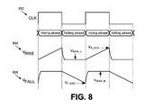
- FIG. 8 shows the signaling at nodes 716 (V RISE ) and 736 (V FALL ).
- Graph 802 shows the clock signal.
- Graph 804 shows the voltage trace at node 716 and graph 806 shows the voltage trace at node 736 .
- the voltage V RISE rises from V BIAS — L up to V R — END
- the voltage V FALL falls from V BIAS — H down to V F — END . Since it is desirable to have a triangular wave with no discontinuities at the boundary between the rising and falling phases, constraints on the ramp slope (set by current sources and capacitors) and the ramp amplitude (set by the bias voltages V BIAS — H and V BIAS — L ) are established. Specifically V R — END should equal V BIAS — H and V F — END should equal V BIAS — L .
- I DC is the current supplied by the current source
- C is the capacitance of the capacitor in each sawtooth generator. Since each charging or discharging phase lasts for half a clock period and the voltage swing is set by V BIAS — H and V BIAS — L , the following constraint between the ramp slope and the voltage swing is derived:
- the design variables are not perfectly controlled or fixed.
- the clock frequency f CLK can have a an error, or the system designer may want flexibility in setting the frequency, in which case the ramp discontinuities would increase as the clock frequency deviates from the nominally assumed value.
- the clock frequency is fixed and ideally known, process and temperature variations in either the ramp slope or the bias voltages can cause large discontinuities.
- bias voltages V BIAS — H and V BIAS — L are created by forcing a DC current through a string of on-chip resistors.
- the ramp slope is inversely proportional to on-chip resistance (via the inverse relationship to I DC ) and the on-chip capacitor.
- Typical semiconductor processes will have resistors that exhibit process variations in the 20-30% range. Since on-chip capacitor variation is in general not well correlated with resistance, the process variations will not cancel one another and the ramp slope will exhibit a large variation.
- FIG. 9 shows an embodiment of the effect of process variation on the ramp signal while maintaining a nominal clock frequency.
- Trace 902 shows a nominal clock signal.
- Trace 904 is an ideal nominal case ramp signal while trace 906 and trace 908 are fast and slow process corners, respectively.
- on-chip resistance is lower than nominal. Since it was previously shown that ramp slope is inversely proportional to resistance, in the fast corner the ramp slope is greater than nominal and trace 906 shows a large overshoot. In the slow corner, the resistance is larger than nominal and the resulting ramp slope is too low; this condition results in trace 908 .
- FIG. 10 illustrates an embodiment in which errors between the clock frequency and the ramp slope result in similar discontinuities in the triangular waveform.
- Trace 1002 shows a nominal clock and trace 1004 shows the resultant ramp waveform where the ramp slope is matched to the clock frequency.
- Trace 1012 shows a clock signal running faster than the nominal clock shown in trace 1002 , and trace 1014 is the resultant ramp waveform. Since the ramp slope was optimized for the nominal clock frequency, the slope is too low for the faster clock and the capacitor voltage won't reach the proper final voltage when the next ramp phase is initiated. This causes the voltage “jump” seen in circled region 1016 .
- Trace 1022 shows a clock signal running slower than the nominal clock shown in trace 1002 , and trace 1024 shows the resultant ramp waveform. In this case the ramp slope is too high and the ramp voltage overshoots the bias levels.
- Circled region 1026 shows a “jump” in the waveform.
- FIG. 11 diagrams how discontinuities in the triangular waveform can result in PWM errors.
- Graph 1102 shows an ideal triangular ramp waveform while graph 1104 shows a triangular ramp with a large voltage discontinuity at the ramp peaks.
- Graph 1106 shows the PWM signal resulting from the ideal triangular waveform and graph 1108 shows the PWM signal resulting from the triangular waveform with discontinuities which causes the PWM's rising edge to occur too soon.
- timing errors such as these result in a dramatic loss of linearity.
- FIG. 12 is an embodiment of a programmable-frequency self-oscillating triangle wave generator 1200 using the basic architecture of triangle wave generator 700 .
- the wave generator 1200 comprises triangle wave generator 1220 , comparator 1206 , comparator 1208 , and RS latch 1210 .
- Triangle wave generator 1220 comprises a rising sawtooth generator 1240 and a falling sawtooth generator 1250 .
- Rising sawtooth generator 1240 is coupled to V BIAS — L at 704 and comprises switch 706 , switch 708 , and capacitor 710 .
- Falling sawtooth generator 1250 is coupled to V BIAS — H at 724 and comprises switch 726 , switch 728 , and capacitor 730 .
- the rising sawtooth generator 1240 and the falling sawtooth generator 1250 are alternatively coupled to output 740 of triangle wave generator 1220 via complementary switches 712 and 732 .
- Triangle wave generator 1220 differs from triangle wave generator 700 in that adjustable current source 1202 replaces current source 702 and adjustable current source 1204 replaces current source 722 .
- the adjustable current sources are implemented using a current DAC which receives a digital value cal_code and produces a current ICAL based on the digital value.
- Comparators 1206 and 1208 combined with latch 1210 are essentially an exemplary embodiment of a digital pulse generator that generates a clock signal with essentially the same frequency as the triangular waveform generated at the output.
- Comparator 1206 compares the output voltage V RAMP against high bias voltage V BIAS — H supplied at 1214
- comparator 1208 compares the output voltage V RAMP against low bias voltage V BIAS — L supplied at 1212 .
- V RAMP reaches V BIAS — H
- comparator 1206 sends a high signal to the “reset” input of RS latch 1210 forcing the latch to generate a low signal.
- comparator 1208 sends a high signal to the “set” input of RS latch 1210 forcing the latch to generate a high signal.
- Output 1216 of RS latch 1210 is used as a clock to operate the switches in triangle wave generator 1220 .
- FIG. 13 shows an example of the signaling of self-oscillating triangle wave generator 1200 . It shows the V RAMP signal shown as trace 1302 in relationship to the outputs of comparator 1206 (CompH OUT ) shown as trace 1304 and comparator 1208 (CompL OUT ) shown as trace 1306 as well as to the RS latch 1210 output (CLK) shown as trace 1308 .
- comparator 1206 ComparpH OUT
- Comparor 1208 Comparor 1208
- CLK RS latch 1210 output
- self-oscillating triangle wave generator 1200 generates a triangle wave with minimal, if any, discontinuity.
- the slope of the rising and falling segments of the triangle waveform is directly proportional to the DC current applied to the capacitors, i.e. increasing the DC current results in the slope increasing. If the slope of V RAMP were increased, the period between threshold crossings would decrease proportionally. Thus the frequency of the ramp and associated clock will also increase. The opposite occurs if the DC current is decreased. Lower DC current causes lower ramp slope, which results in a longer ramp period or lower frequency. Since self-oscillating triangle wave generator 1200 is effectively a programmable oscillator, I CAL can be calibrated to the appropriate current level needed to match the wave generator's frequency to a desired incoming clock frequency.
- FIG. 14 shows an embodiment of a triangle wave generator with calibration.
- a triangle wave generator 1400 comprises self-oscillating triangle wave generator 1200 and calibration circuit 1402 .
- Calibration circuit 1402 receives clock signal CLK 1216 from wave generator 1200 and synchronization clock signal CLK_IN. By measuring the differences between CLK and CLK_IN, calibration circuit 1402 adjusts the frequency of wave generator 1200 to match CLK_IN by altering the DC current supplied by current sources 1202 and 1204 .
- calibration circuit 1402 operates using a feedback mechanism that attempts to force CLK to match CLK_IN.
- FIG. 15 shows an embodiment of a triangle wave generator with an example calibration circuit.
- triangle wave generator 1500 comprises a calibration circuit with rate comparison circuit 1510 and successive-approximation-register (SAR) logic 1508 .
- Comparison circuit 1510 comprises reference counter 1502 , comparison circuit 1504 , and ramp counter 1506 .
- Reference counter 1502 counts CLK_IN clock cycles and ramp counter 1506 counts CLK clock cycles.
- Comparison circuit 1504 in conjunction with reference counter 1502 acts as a timer to enable ramp counter 1506 for N periods of the CLK_IN signal, so that after N periods a determination can be made as to whether the CLK signal has a higher or lower frequency than the CLK_IN signal.
- SAR logic 1508 determines the calibration value “cal_code” which results in a CLK signal which most closely matches the CLK_IN signal in frequency.
- FIG. 16 is a flowchart illustrating an embodiment of the operation of the SAR logic block.
- a binary search is initialized by setting cal_code to all zeros and setting n equal to B, the number of bits in cal_code.
- the n th bit of cal_code is set to 1.
- a determination is made as to whether CLK is faster than CLK_IN. This can be performed by rate comparison circuit 1510 . If true, the n th bit of cal_code is reset to 0 at step 1608 and then step 1610 is executed.
- step 1606 If at step 1606 the CLK signal is slower than the CLK_IN signal, the n th bit is left high and step 1610 is executed.
- step 1610 a determination is made as to whether n is greater than 1, i.e. the process has reached the lowest bit of cal_code. If n is greater than 1, n is decremented at step 1612 and the process repeats on the next significant bit by returning to step 1604 . If at step 1610 n is not greater than 1, the calibration operation is complete and the cal_code value which yields the closest frequency match between CLK and CLK_IN has been found and is frozen by the SAR logic block at step 1614 .
- N should be greater than 2 B .
- this code yields a CLK frequency that is lower than CLK_IN's frequency; the 5 th bit then remains set high.
- this code also yields a CLK frequency that is lower than CLK_IN's frequency; then the 4 th bit remains set high.
- triangle wave generator 1220 will not be precisely synchronized with CLK_IN. Even if there was no frequency error between the two clock signals, there may still be a phase shift between the two. In one embodiment, after calibration is complete, the triangle wave generator 1220 is driven with CLK_IN to synchronize the resultant triangle wave signal V RAMP with CLK_IN while maintaining minimal discontinuities.
- FIG. 17 shows an embodiment of a programmable triangle wave generator that can be switched to be synchronized and driven by an external clock signal.
- Programmable triangle wave generator 1700 is similar to self-oscillating triangle wave generator 1200 , but further comprises selection circuitry shown in this example by multiplexer 1702 .
- the multiplexer's input select is set to one and the internally generated clock signal comp clk is used to drive triangle generator 1220 .
- the output of the multiplexer, signal 1704 can be sent to the calibration circuitry.
- multiplexer 1702 can be set to select the external clock signal CLK_IN to drive triangle wave generator 1220 , thus producing an output signal which is a triangle wave synchronized to CLK_IN.
- FIG. 18 shows an embodiment of the programmable triangle wave generator with calibration circuitry. The components are described previously in FIGS. 12 , 15 , and 17 .
- cal_en can also be used to indicate when calibration has completed. When the cal_en signal is in the low state, calibration is complete and the calibration circuitry as well as comparators 1206 and 1208 and latch 1210 can be disabled to save power.
- FIGS. 19 and 20 Simulation results of a calibration system employing a 6-bit current DAC are shown in FIGS. 19 and 20 .
- FIG. 20 plots the magnitude of the discontinuities normalized to ramp amplitude with and without calibration.
- a positive error indicates that the discontinuity is due to a ramp voltage that overshoots the bias voltages (see graph 906 of FIG. 9 for an example).
- a negative error indicates that the ramp voltage was lower than the bias voltages (see graph 908 of FIG. 9 ).
- the dashed trace 2002 shows how the voltage discontinuities of an uncalibrated ramp generator increase dramatically as process variation skews away from nominal. At high positive variations where the ramp slope is too low, the ramp voltage undershoots the ideal voltage by over 15%.
- Solid trace 2004 shows the magnitude of the discontinuities after calibration has been performed. The error is now bounded to less than 1.5% across the variation range.
Abstract
Description
- 1. Field of the Invention
- The present invention relates generally to pulse width modulation (PWM) and class-D amplifiers and specifically to clock-synchronized triangular waveform generators.
- 2. Related Art
- Power delivery systems such as power amplifiers, switching voltage regulators, and electric motors often employ pulse-width modulation (PWM) to convey information or deliver power in an efficient manner. For example, class-D amplifiers employing PWM are used in powered audio devices due to their advantages in power consumption and size over traditional analog amplifiers. The improved power efficiency reduces the need for bulky heat sinks or advanced packaging, making class-D amplifiers more suitable for low-cost integrated circuits.
- The class-D amplifier produces an output comprising a sequence of pulses. Pulse-width modulation is typically employed to encode audio information into these pulses by varying their individual widths. The average value of these pulses represents the instantaneous amplitude of the output signal. These pulses also introduce unwanted high-frequency content which may be removed by a low pass filter.
-
FIG. 1 is a block diagram illustrating the typical architecture of a class-D amplifier 100. The input signal is converted topulses using modulator 102 which can be a pulse-width modulator. A common implementation of a pulse-width modulator uses a high-speed comparator to compare the input signal against a triangle wave. The modulated signal is then amplified byamplifier 104 and finally demodulated bylow pass filter 106. The demodulated signal can then be used, for example byspeaker 108. -
FIG. 2 shows a typical PWM generator.Input reference signal 202 is compared bycomparator 206 against a repetitive modulation source, such as a sawtooth or triangular waveform generated byramp generator 204. When the input reference signal is greater than the modulation source, the signal level ofPWM output signal 208 is high; when the input reference signal is less than the modulation source, the signal level ofPWM output signal 208 is low. - In communication systems using class-D audio amplifiers, PWM performance is optimized for peak amplifier linearity. For a given modulation frequency, PWM performance is improved when the modulating source is a triangular waveform instead of a sawtooth.
FIG. 3A shows traces of the signals related to a PWM generator using a sawtooth waveform.Graph 302 shows the sawtooth modulation source superimposed on the input reference signal.Graph 304 shows the resultant PWM output signal.FIG. 3B shows traces of the signals related to a PWM generator using a triangular waveform. Graph 312 shows the triangular modulation source superimposed on the input reference signal.Graph 314 shows the resultant PWM output signal. Because reference information is encoded on both the rising and falling edges ofPWM signal 314, as opposed to only one edge ofPWM signal 304 when a sawtooth modulating source is employed, a triangular waveform is a preferable modulation source. - In a typical class-D audio amplifier system, the input audio signal is an analog waveform reconstructed from digital samples. In order to reduce spectral folding and aliasing issues, it is desirable to have the triangular waveform synchronized to a frequency related to the sampling clock. Usually the sampling clock is a divided down version of a master clock. To avoid the aforementioned issues, the triangular waveform should be synchronized to another clock that is also divided down from the same master clock.
- Other challenges with the design of a synchronized triangular waveform generator include drift due to the triangle wave not returning to the same voltage level after each clock cycle, synchronization where the triangle waveform frequency does not match the clock rate of a given input clock, and linearity in either the upward ramp or downward ramp of the triangle waveform. Therefore, there is a need in the industry for an inexpensive and improved clock-synchronized triangular waveform generator.
- In a pulse modulator, a calibrated synchronized triangular waveform generator has a triangular waveform generator, a digital pulse generator which generates a square wave clock signal with essentially the same frequency as the generated triangle waveform, and a calibration circuit. During a calibration phase, the clock signal produced by the digital pulse generator is compared with an external clock signal and the triangular waveform generator is adjusted by the calibration circuit until the generated clock signal matches as close as possible to the external clock signal.
- The calibrated synchronized triangular waveform generator can further include a clock selection circuit which selects the clock signal generated during calibration and the external clock signal at other times, with the selected clock signal fed back to the triangular waveform generator. One embodiment of the digital pulse generator has two comparators and an RS latch. After calibration the digital pulse generator and the calibration circuit can be deactivated to save power. The calibration circuit can have a rate comparison circuit and a successive-approximation-register (SAR) logic block for adjusting the calibration code used by the triangular waveform generator. The triangular waveform generator can have a rising sawtooth waveform generator and a falling sawtooth waveform generator with complementary switching circuits that alternatively select the rising sawtooth waveform and the falling sawtooth waveform to generate the triangular waveform.
- Other systems, methods, features, and advantages of the present disclosure will be or become apparent to one with skill in the art upon examination of the following drawings and detailed description. It is intended that all such additional systems, methods, features, and advantages be included within this description, be within the scope of the present disclosure, and be protected by the accompanying claims.
- Many aspects of the disclosure can be better understood with reference to the following drawings. The components in the drawings are not necessarily to scale, emphasis instead being placed upon clearly illustrating the principles of the present disclosure. Moreover, in the drawings, like reference numerals designate corresponding parts throughout the several views.
-
FIG. 1 is a block diagram illustrating the typical architecture of a class-D amplifier; -
FIG. 2 shows a typical PWM generator; -
FIG. 3A shows traces of the signals related to a PWM generator using a sawtooth modulation waveform; -
FIG. 3B shows traces of the signals related to a PWM generator using a triangular modulation waveform; -
FIG. 4 shows a synchronized triangular waveform generator; -
FIG. 5 shows a relation between the modulation clock and the switch control signals in the synchronized triangular waveform generator ofFIG. 4 ; -
FIG. 6 shows the case of voltage drift due to circuit non-idealities; -
FIG. 7 shows an embodiment of a synchronized triangular waveform generator which does not have voltage drift; -
FIG. 8 shows the signaling of the two sawtooth generators; -
FIG. 9 shows the effect of process variation on the ramp signal while maintaining a nominal clock frequency; -
FIG. 10 shows the effect of errors between the clock frequency and the nominal ramp slope; -
FIG. 11 diagrams how discontinuities in the triangular waveform can result in PWM errors; -
FIG. 12 is a self-oscillating triangle wave generator; -
FIG. 13 shows an example of the signaling of a self-oscillating triangle wave generator; -
FIG. 14 shows an embodiment of a triangle wave generator with calibration; -
FIG. 15 shows an embodiment of a triangle wave generator with an example of a calibration circuit; -
FIG. 16 shows a flowchart of the operation of the SAR logic block; -
FIG. 17 shows an embodiment of a programmable triangle wave generator which can be switched to use an external clock signal; -
FIG. 18 shows an embodiment of the programmable triangle wave generator with calibration circuitry; -
FIG. 19 shows how the calibration code varies versus the on-chip resistor variation; and -
FIG. 20 plots the magnitude of the discontinuities normalized to ramp amplitude with and without calibration. - A detailed description of embodiments of the present invention is presented below. While the disclosure will be described in connection with these drawings, there is no intent to limit it to the embodiment or embodiments disclosed herein. On the contrary, the intent is to cover all alternatives, modifications, and equivalents included within the spirit and scope of the disclosure.
-
FIG. 4 shows a synchronized triangular waveform generator.Triangular waveform generator 400 comprises fixedcurrent source 402, fixedcurrent source 404 andcapacitor 410.Waveform generator 400 also comprises complementary switching circuits shown in this example byswitch 406 and switch 408 which are switched in a complementary fashion such that whenswitch 406 is open,switch 408 is closed, and vice versa. A bias voltage is applied at 412 totriangular waveform generator 400.Switch 406 is controlled by signal SWr and switch 408 is controlled by signal SWf. As shown inFIG. 5 ,switch 406 is synchronized to a modulation clock signal such that when the clock signal ishigh switch 406 is closed and when the clock signal islow switch 406 is opened.Complementary switch 408 is opened when the clock signal is high and closed with the clock signal is low. - When
switch 406 is closed and switch 408 is open,current source 404 charges capacitor 410 linearly until the next clock transition. When the clock goes low,switch 408 closes and switch 406 opens, allowingcurrent source 402 to dischargecapacitor 410 linearly. With substantially equal charge and discharge times (i.e. the modulation clock has a 50% duty-cycle) and matched current sources (the current drawn bycurrent source 402 is the same as the current driven by current source 404), the voltage atnode 414 is bounded between a peak ramp voltage VRAMP— H and the bias voltage VBIAS. - Imperfections in clock or switch timing or current source magnitudes can result in an undesirable mismatch between the charge transferred during the “charge” and “discharge” phases. For example, a charge error generated each clock period can accumulate over time resulting in a voltage drift towards one of the power rails and an eventual saturation.
FIG. 6 shows the case where the discharging current is slightly greater than the charging current, which causes the slope of the falling phase to be slightly greater than the slope of the rising phase. The ramp voltage drifts lower over each clock period, causing the waveform's common-mode voltage to vary over time. For proper operation using this arrangement a correction scheme to manage this drift may be used. -
FIG. 7 shows an embodiment of a synchronized triangular waveform generator which doesn't have the drift issue described previously.Waveform generator 700 employs two circuits, a risingsawtooth generator 710 and a fallingsawtooth generator 720, to generate separate rising and falling sawtooth waveforms. Each sawtooth generator is alternately connected tooutput 740 throughswitch 714 and switch 734, respectively, to capture the rising and falling edges to form a triangular waveform. Therefore, the voltage VRAMP seen atoutput 740 is the rising voltage VRISE atoutput node 716 generated by risingsawtooth generator 710 whenswitch 714 is closed and is the falling voltage VFALL atoutput node 736 generated by fallingsawtooth generator 720 whenswitch 734 is closed.Switch 714 is controlled by a clock signal CLK andcomplementary switch 734 is controlled by the inverted clock signal CLK. - Rising
sawtooth generator 710 comprisescurrent source 702,complementary switches 706 and 708, andcapacitor 712, and is coupled to low bias voltage VBIAS— L at 704. When switch 706 is closed and switch 708 is opened, the voltage atnode 716 rises linearly from the low bias voltage due tocurrent source 702 chargingcapacitor 712. This generates the linear rising portion of the triangle wave seen atoutput 740. Whenswitch 708 is closed and switch 706 is opened,capacitor 712 is pre-charged back to the bias voltage VBIAS— L. During this pre-charge portion of the rising sawtooth generator's cycle,node 716 is disconnected fromoutput 740 byswitch 714. - Similarly, falling
sawtooth generator 720 comprisescurrent source 722,complementary switches 726 and 728, andcapacitor 732, and is coupled to high bias voltage VBIAS— H at 724. Whenswitch 726 is closed and switch 728 is opened, the voltage atnode 736 falls linearly from the high bias voltage due tocurrent source 722 dischargingcapacitor 732. This generates the linear falling portion of the triangle wave seen atoutput 740. When switch 728 is closed and switch 726 is opened,capacitor 732 is pre-charged back to the bias voltage VBIAS— H. During this pre-charge portion of the falling sawtooth generator's cycle,node 736 is disconnected fromoutput 740 byswitch 734. - While
wave generator 700 does not suffer the drawback of voltage drift since the capacitors are pre-charged to fixed voltages each cycle, there may be voltage discontinuities. Unlike the voltage drift problems discussed with reference toFIG. 4 , errors from such discontinuities inwave generator 700 do not accumulate or grow over time as it does inwaveform generator 400. -
FIG. 8 shows the signaling at nodes 716 (VRISE) and 736 (VFALL).Graph 802 shows the clock signal.Graph 804 shows the voltage trace atnode 716 andgraph 806 shows the voltage trace atnode 736. The voltage VRISE rises from VBIAS— L up to VR— END, while the voltage VFALL falls from VBIAS— H down to VF— END. Since it is desirable to have a triangular wave with no discontinuities at the boundary between the rising and falling phases, constraints on the ramp slope (set by current sources and capacitors) and the ramp amplitude (set by the bias voltages VBIAS— H and VBIAS— L) are established. Specifically VR— END should equal VBIAS— H and VF— END should equal VBIAS— L. - In order to set the ramp slope properly, the relationship between the ramp phases and the bias voltages is determined. During a ramp phase a capacitor is either being charged or discharged by a constant current source. The voltage change across this capacitor can be written as:
-
- where the ramp slope is defined as
-
- IDC is the current supplied by the current source, and C is the capacitance of the capacitor in each sawtooth generator. Since each charging or discharging phase lasts for half a clock period and the voltage swing is set by VBIAS
— H and VBIAS— L, the following constraint between the ramp slope and the voltage swing is derived: -
- If the previous relationship holds, then there will be no discontinuities in the triangular waveform. However in practice the design variables are not perfectly controlled or fixed. For example, the clock frequency fCLK can have a an error, or the system designer may want flexibility in setting the frequency, in which case the ramp discontinuities would increase as the clock frequency deviates from the nominally assumed value. Even if the clock frequency is fixed and ideally known, process and temperature variations in either the ramp slope or the bias voltages can cause large discontinuities.
- In order to generate process and temperature independent bias voltages, in one embodiment bias voltages VBIAS
— H and VBIAS— L are created by forcing a DC current through a string of on-chip resistors. The resulting bias voltage is VBIAS=IBIASR, where R is the resistance of the on-chip resistors. If IBIAS is a current source that is made inversely proportional to the on-chip resistance, the resistance variations cancel out and the bias voltage can be made insensitive to process and temperature variations. Since the triangle wave oscillates between the two bias voltages, the ramp amplitude is consequently also made process and temperature independent. - Previously the ramp slope was defined to be
-
- hence the ramp slope is inversely proportional to on-chip resistance (via the inverse relationship to IDC) and the on-chip capacitor. Typical semiconductor processes will have resistors that exhibit process variations in the 20-30% range. Since on-chip capacitor variation is in general not well correlated with resistance, the process variations will not cancel one another and the ramp slope will exhibit a large variation.
-
FIG. 9 shows an embodiment of the effect of process variation on the ramp signal while maintaining a nominal clock frequency.Trace 902 shows a nominal clock signal.Trace 904 is an ideal nominal case ramp signal whiletrace 906 and trace 908 are fast and slow process corners, respectively. In the fast corner, on-chip resistance is lower than nominal. Since it was previously shown that ramp slope is inversely proportional to resistance, in the fast corner the ramp slope is greater than nominal and trace 906 shows a large overshoot. In the slow corner, the resistance is larger than nominal and the resulting ramp slope is too low; this condition results intrace 908. -
FIG. 10 illustrates an embodiment in which errors between the clock frequency and the ramp slope result in similar discontinuities in the triangular waveform.Trace 1002 shows a nominal clock andtrace 1004 shows the resultant ramp waveform where the ramp slope is matched to the clock frequency.Trace 1012 shows a clock signal running faster than the nominal clock shown intrace 1002, andtrace 1014 is the resultant ramp waveform. Since the ramp slope was optimized for the nominal clock frequency, the slope is too low for the faster clock and the capacitor voltage won't reach the proper final voltage when the next ramp phase is initiated. This causes the voltage “jump” seen in circledregion 1016.Trace 1022 shows a clock signal running slower than the nominal clock shown intrace 1002, andtrace 1024 shows the resultant ramp waveform. In this case the ramp slope is too high and the ramp voltage overshoots the bias levels. Circledregion 1026 shows a “jump” in the waveform. - Ramp discontinuities can cause errors in the PWM generation, which can reduce system performance.
FIG. 11 diagrams how discontinuities in the triangular waveform can result in PWM errors.Graph 1102 shows an ideal triangular ramp waveform whilegraph 1104 shows a triangular ramp with a large voltage discontinuity at the ramp peaks.Graph 1106 shows the PWM signal resulting from the ideal triangular waveform andgraph 1108 shows the PWM signal resulting from the triangular waveform with discontinuities which causes the PWM's rising edge to occur too soon. In applications such as class-D amplifiers where signal integrity is important across large modulation ranges (e.g., modulation indexes approaching 100%), timing errors such as these result in a dramatic loss of linearity. -
FIG. 12 is an embodiment of a programmable-frequency self-oscillatingtriangle wave generator 1200 using the basic architecture oftriangle wave generator 700. Thewave generator 1200 comprisestriangle wave generator 1220,comparator 1206,comparator 1208, andRS latch 1210.Triangle wave generator 1220 comprises a risingsawtooth generator 1240 and a fallingsawtooth generator 1250. Risingsawtooth generator 1240 is coupled to VBIAS— L at 704 and comprises switch 706,switch 708, andcapacitor 710. Fallingsawtooth generator 1250 is coupled to VBIAS— H at 724 and comprisesswitch 726, switch 728, andcapacitor 730. The risingsawtooth generator 1240 and the fallingsawtooth generator 1250 are alternatively coupled tooutput 740 oftriangle wave generator 1220 viacomplementary switches Triangle wave generator 1220 differs fromtriangle wave generator 700 in that adjustablecurrent source 1202 replacescurrent source 702 and adjustablecurrent source 1204 replacescurrent source 722. In one embodiment, the adjustable current sources are implemented using a current DAC which receives a digital value cal_code and produces a current ICAL based on the digital value. -
Comparators latch 1210 are essentially an exemplary embodiment of a digital pulse generator that generates a clock signal with essentially the same frequency as the triangular waveform generated at the output.Comparator 1206 compares the output voltage VRAMP against high bias voltage VBIAS— H supplied at 1214, andcomparator 1208 compares the output voltage VRAMP against low bias voltage VBIAS— L supplied at 1212. When VRAMP reaches VBIAS— H,comparator 1206 sends a high signal to the “reset” input of RS latch 1210 forcing the latch to generate a low signal. When VRAMP falls to VBIAS— L,comparator 1208 sends a high signal to the “set” input of RS latch 1210 forcing the latch to generate a high signal.Output 1216 ofRS latch 1210 is used as a clock to operate the switches intriangle wave generator 1220. -
FIG. 13 shows an example of the signaling of self-oscillatingtriangle wave generator 1200. It shows the VRAMP signal shown astrace 1302 in relationship to the outputs of comparator 1206 (CompHOUT) shown astrace 1304 and comparator 1208 (CompLOUT) shown astrace 1306 as well as to theRS latch 1210 output (CLK) shown astrace 1308. When the clock signal is high, the risingsawtooth generator 1240 causes VRAMP to rise. When VRAMP reaches VBIAS— H, CompHOUT goes high causing RS latch 1210 to force CLK low. When the clock goes low, the switches intriangle wave generator 1220 connect the fallingsawtooth generator 1250 tooutput 740, causing VRAMP to fall linearly until VRAMP reaches VBIAS— L. When VRAMP reaches VBIAS— L, CompLOUT goes high causing RS latch 1210 to force CLK high. This causes the switches intriangle wave generator 1220 to connect risingsawtooth generator 1240 tooutput 740 and the process thus repeats. - In this embodiment, self-oscillating
triangle wave generator 1200 generates a triangle wave with minimal, if any, discontinuity. The slope of the rising and falling segments of the triangle waveform is directly proportional to the DC current applied to the capacitors, i.e. increasing the DC current results in the slope increasing. If the slope of VRAMP were increased, the period between threshold crossings would decrease proportionally. Thus the frequency of the ramp and associated clock will also increase. The opposite occurs if the DC current is decreased. Lower DC current causes lower ramp slope, which results in a longer ramp period or lower frequency. Since self-oscillatingtriangle wave generator 1200 is effectively a programmable oscillator, ICAL can be calibrated to the appropriate current level needed to match the wave generator's frequency to a desired incoming clock frequency. -
FIG. 14 shows an embodiment of a triangle wave generator with calibration. Atriangle wave generator 1400 comprises self-oscillatingtriangle wave generator 1200 andcalibration circuit 1402.Calibration circuit 1402 receivesclock signal CLK 1216 fromwave generator 1200 and synchronization clock signal CLK_IN. By measuring the differences between CLK and CLK_IN,calibration circuit 1402 adjusts the frequency ofwave generator 1200 to match CLK_IN by altering the DC current supplied bycurrent sources calibration circuit 1402 operates using a feedback mechanism that attempts to force CLK to match CLK_IN. -
FIG. 15 shows an embodiment of a triangle wave generator with an example calibration circuit. In this embodiment,triangle wave generator 1500 comprises a calibration circuit withrate comparison circuit 1510 and successive-approximation-register (SAR)logic 1508.Comparison circuit 1510 comprisesreference counter 1502,comparison circuit 1504, andramp counter 1506.Reference counter 1502 counts CLK_IN clock cycles andramp counter 1506 counts CLK clock cycles.Comparison circuit 1504 in conjunction withreference counter 1502 acts as a timer to enableramp counter 1506 for N periods of the CLK_IN signal, so that after N periods a determination can be made as to whether the CLK signal has a higher or lower frequency than the CLK_IN signal. If fewer than N cycles of the CLK signal are counted after N periods of the CLK_IN signal are counted, then the CLK signal has a lower frequency than the CLK_IN signal. Similarly, if the count determined byramp counter 1506 is greater than N at the end of N periods of the CLK_IN signal, then CLK has a higher frequency than the CLK_IN signal.SAR logic 1508 uses this information to adjust the CLK signal. - In one embodiment,
SAR logic 1508 determines the calibration value “cal_code” which results in a CLK signal which most closely matches the CLK_IN signal in frequency.FIG. 16 is a flowchart illustrating an embodiment of the operation of the SAR logic block. Atstep 1602, a binary search is initialized by setting cal_code to all zeros and setting n equal to B, the number of bits in cal_code. Atstep 1604, the nth bit of cal_code is set to 1. Atstep 1606, a determination is made as to whether CLK is faster than CLK_IN. This can be performed byrate comparison circuit 1510. If true, the nth bit of cal_code is reset to 0 atstep 1608 and then step 1610 is executed. If atstep 1606 the CLK signal is slower than the CLK_IN signal, the nth bit is left high andstep 1610 is executed. Atstep 1610, a determination is made as to whether n is greater than 1, i.e. the process has reached the lowest bit of cal_code. If n is greater than 1, n is decremented atstep 1612 and the process repeats on the next significant bit by returning to step 1604. If at step 1610 n is not greater than 1, the calibration operation is complete and the cal_code value which yields the closest frequency match between CLK and CLK_IN has been found and is frozen by the SAR logic block atstep 1614. - In order to obtain an accurate comparison, N should be greater than 2B. To demonstrate this process, suppose cal_code is a six-bit code such that B=6. Because N should be greater than 26=64, a choice of N=128 is convenient. The process begins by setting cal_code to [100000]. Assuming that this code yields a CLK frequency that is higher than CLK_IN's frequency (i.e., the output of
ramp counter 1506 is greater than 128), then the highest bit is cleared, i.e. cal_code=[000000]. Note that bits in bold text designate code bits that have been determined and are fixed for the remainder of the calibration procedure. On the next iteration, the 5th bit is set high and cal_code=[010000]. Suppose that this code yields a CLK frequency that is lower than CLK_IN's frequency; the 5th bit then remains set high. On the next iteration, the 4th bit is set high and cal_code=[011000]. Suppose that this code also yields a CLK frequency that is lower than CLK_IN's frequency; then the 4th bit remains set high. On the following iteration, the 3rd bit is set high such that cal_code=[011100]. If this code results in a CLK frequency that is higher than CLK_IN's frequency, then the 3rd bit is cleared, i.e. cal_code=[011000]. Continuing to the next iteration, the 2nd bit is set high so cal_code=[011010]. Assuming that this code yields a CLK frequency lower than CLK_IN's frequency, then the 2nd bit remains set high. On the last iteration, the 1st bit is set high and cal_code=[011011]. If this code results in a CLK frequency that is higher than CLK_IN's frequency, then the 1st bit is cleared low, thus leaving the calibration code set to a final value of cal_code=[011010]. - Because it is likely that the frequency of CLK_IN and the frequency of a calibrated CLK will not be exactly the same,
triangle wave generator 1220 will not be precisely synchronized with CLK_IN. Even if there was no frequency error between the two clock signals, there may still be a phase shift between the two. In one embodiment, after calibration is complete, thetriangle wave generator 1220 is driven with CLK_IN to synchronize the resultant triangle wave signal VRAMP with CLK_IN while maintaining minimal discontinuities. -
FIG. 17 shows an embodiment of a programmable triangle wave generator that can be switched to be synchronized and driven by an external clock signal. Programmabletriangle wave generator 1700 is similar to self-oscillatingtriangle wave generator 1200, but further comprises selection circuitry shown in this example bymultiplexer 1702. During calibration, the multiplexer's input select is set to one and the internally generated clock signal comp clk is used to drivetriangle generator 1220. The output of the multiplexer,signal 1704, can be sent to the calibration circuitry. After calibration is complete,multiplexer 1702 can be set to select the external clock signal CLK_IN to drivetriangle wave generator 1220, thus producing an output signal which is a triangle wave synchronized to CLK_IN. -
FIG. 18 shows an embodiment of the programmable triangle wave generator with calibration circuitry. The components are described previously inFIGS. 12 , 15, and 17. In addition to the cal_en signal enabling calibration and controlling which clock signal drivestriangle wave generator 1220, cal_en can also be used to indicate when calibration has completed. When the cal_en signal is in the low state, calibration is complete and the calibration circuitry as well ascomparators latch 1210 can be disabled to save power. - Simulation results of a calibration system employing a 6-bit current DAC are shown in
FIGS. 19 and 20 .FIG. 19 shows how the calibration code varied versus the on-chip resistor variation. The plot shows that the calibration was monotonic with variation, as expected. Under nominal conditions, cal_code=32 which was at the midpoint of its range (0-63). At high positive variations, on-chip resistance is higher than nominal; thus the ramp slope is lower than ideal. The calibration then correctly determined that a higher DAC current was needed to increase the ramp slope. -
FIG. 20 plots the magnitude of the discontinuities normalized to ramp amplitude with and without calibration. A positive error indicates that the discontinuity is due to a ramp voltage that overshoots the bias voltages (seegraph 906 ofFIG. 9 for an example). A negative error indicates that the ramp voltage was lower than the bias voltages (seegraph 908 ofFIG. 9 ). The dashedtrace 2002 shows how the voltage discontinuities of an uncalibrated ramp generator increase dramatically as process variation skews away from nominal. At high positive variations where the ramp slope is too low, the ramp voltage undershoots the ideal voltage by over 15%.Solid trace 2004 shows the magnitude of the discontinuities after calibration has been performed. The error is now bounded to less than 1.5% across the variation range. - Additional simulations on other variations such as temperature, frequency deviation, and capacitance show similar behavior. The calibration has the added benefit that it isn't sensitive to errors in the DAC. DAC offset or non-linearity is not of vital importance since the calibration logic's binary search will always seek out the optimal DAC setting from what is available. The only constraint on the DAC is that it be monotonic, which is easily achieved in practice.
- The above-described embodiments are merely examples of possible implementations. Many variations and modifications may be made to the above-described embodiments without departing from the principles of the present disclosure. All such modifications and variations are intended to be included herein within the scope of this disclosure and protected by the following claims.
Claims (20)
Priority Applications (1)
| Application Number | Priority Date | Filing Date | Title |
|---|---|---|---|
| US12/574,663 US8044690B2 (en) | 2009-10-06 | 2009-10-06 | System and method for clock-synchronized triangular waveform generation |
Applications Claiming Priority (1)
| Application Number | Priority Date | Filing Date | Title |
|---|---|---|---|
| US12/574,663 US8044690B2 (en) | 2009-10-06 | 2009-10-06 | System and method for clock-synchronized triangular waveform generation |
Publications (2)
| Publication Number | Publication Date |
|---|---|
| US20110080191A1 true US20110080191A1 (en) | 2011-04-07 |
| US8044690B2 US8044690B2 (en) | 2011-10-25 |
Family
ID=43822727
Family Applications (1)
| Application Number | Title | Priority Date | Filing Date |
|---|---|---|---|
| US12/574,663 Active 2029-11-06 US8044690B2 (en) | 2009-10-06 | 2009-10-06 | System and method for clock-synchronized triangular waveform generation |
Country Status (1)
| Country | Link |
|---|---|
| US (1) | US8044690B2 (en) |
Cited By (12)
| Publication number | Priority date | Publication date | Assignee | Title |
|---|---|---|---|---|
| US20110316508A1 (en) * | 2010-06-28 | 2011-12-29 | Kuang-Yao Cheng | Digital Hybrid V2 Control for Buck Converters |
| US20120326761A1 (en) * | 2011-06-23 | 2012-12-27 | Hon Hai Precision Industry Co., Ltd. | Processor frequency adjustment circuit |
| US20140203726A1 (en) * | 2013-01-22 | 2014-07-24 | Rohm Co., Ltd. | Oscillation circuit |
| US20150022249A1 (en) * | 2013-07-17 | 2015-01-22 | Taiwan Semiconductor Manufacturing Co., Ltd. | Method and apparatus for generating a ramp signal |
| TWI514771B (en) * | 2011-09-08 | 2015-12-21 | Intel Deutschland Gmbh | Triangular waveform generator having differential output synchronized with external clock signal and method for generating a differential trangular waveform |
| CN106405551A (en) * | 2016-11-23 | 2017-02-15 | 福州台江区鸣恒软件技术服务有限公司 | V-FM signal system ISAR two-dimensional imaging method |
| CN107864394A (en) * | 2017-12-11 | 2018-03-30 | 延锋伟世通电子科技(上海)有限公司 | A kind of vehicle-mounted Ethernet AVB synchronous clock generators |
| CN108880211A (en) * | 2018-08-31 | 2018-11-23 | 上海艾为电子技术股份有限公司 | A kind of sawtooth generator, DC-DC converter and electronic equipment |
| CN108964666A (en) * | 2017-05-26 | 2018-12-07 | 立锜科技股份有限公司 | D/A conversion circuit and its digital-to-analogue conversion method |
| CN111884609A (en) * | 2020-08-03 | 2020-11-03 | 广芯电子技术(上海)股份有限公司 | Class D audio power amplifier and sampling triangular wave generating circuit used therein |
| US10958261B2 (en) * | 2017-03-20 | 2021-03-23 | Institute of Microelectronics, Chinese Academy of Sciences | Serial PWM signal decoding circuit and method based on a capacitor charge-discharge structure and method thereof |
| CN117310650A (en) * | 2023-11-28 | 2023-12-29 | 上海孛璞半导体技术有限公司 | Data processing method and device based on FMCW radar |
Families Citing this family (6)
| Publication number | Priority date | Publication date | Assignee | Title |
|---|---|---|---|---|
| EP2388915B1 (en) * | 2010-05-21 | 2013-08-14 | Nxp B.V. | Sawtooth oscillator |
| KR102118349B1 (en) * | 2013-10-31 | 2020-06-04 | 서울시립대학교 산학협력단 | Gate driving circuit, switch apparatus and power supply apparatus having thereof |
| TWI638527B (en) * | 2017-05-17 | 2018-10-11 | 立錡科技股份有限公司 | Digital to analog converter circuit and digital to analog conversion method |
| US10581416B2 (en) * | 2018-06-26 | 2020-03-03 | Texas Instruments Incorporated | External and dual ramp clock synchronization |
| US10782727B2 (en) | 2018-11-19 | 2020-09-22 | Texas Instruments Incorporated | Integrated circuits having self-calibrating oscillators, and methods of operating the same |
| US11152927B1 (en) | 2020-03-25 | 2021-10-19 | Richtek Technology Corporation | Low distortion triangular wave generator circuit and low distortion triangular wave generation method |
Citations (9)
| Publication number | Priority date | Publication date | Assignee | Title |
|---|---|---|---|---|
| US4284906A (en) * | 1979-10-03 | 1981-08-18 | The United States Of America As Represented By The Secretary Of The Navy | Constant amplitude variable frequency synchronized linear ramp generator |
| US4819066A (en) * | 1985-08-29 | 1989-04-04 | Canon Kabushiki Kaisha | Image processing apparatus |
| US6297693B1 (en) * | 1999-12-23 | 2001-10-02 | Red Chip Company Limited | Techniques for synchronizing a self oscillating variable frequency modulator to an external clock |
| US6828753B2 (en) * | 2002-08-26 | 2004-12-07 | International Rectifier Corporation | Input filter for A.C. motor phase current sensing |
| US6982889B2 (en) * | 2002-11-29 | 2006-01-03 | Rohm Co., Ltd | DC/AC converter and its controller IC |
| US20070171684A1 (en) * | 2004-03-05 | 2007-07-26 | Rohm Company, Ltd. | Dc-ac converter controller, ic therefor, and electronic apparatus utilizing such dc-ac converter |
| US20080031028A1 (en) * | 2002-11-29 | 2008-02-07 | Rohm Co., Ltd. | DC-AC Converter and Controller IC Thereof |
| US7554370B2 (en) * | 2003-02-04 | 2009-06-30 | Rohm Co., Ltd. | Method and system for synchronizing phase of triangular signal |
| US7746130B2 (en) * | 2008-07-14 | 2010-06-29 | Elite Semiconductor Memory Technology, Inc. | Triangular wave generating circuit having synchronization with external clock |
-
2009
- 2009-10-06 US US12/574,663 patent/US8044690B2/en active Active
Patent Citations (10)
| Publication number | Priority date | Publication date | Assignee | Title |
|---|---|---|---|---|
| US4284906A (en) * | 1979-10-03 | 1981-08-18 | The United States Of America As Represented By The Secretary Of The Navy | Constant amplitude variable frequency synchronized linear ramp generator |
| US4819066A (en) * | 1985-08-29 | 1989-04-04 | Canon Kabushiki Kaisha | Image processing apparatus |
| US6297693B1 (en) * | 1999-12-23 | 2001-10-02 | Red Chip Company Limited | Techniques for synchronizing a self oscillating variable frequency modulator to an external clock |
| US6828753B2 (en) * | 2002-08-26 | 2004-12-07 | International Rectifier Corporation | Input filter for A.C. motor phase current sensing |
| US6982889B2 (en) * | 2002-11-29 | 2006-01-03 | Rohm Co., Ltd | DC/AC converter and its controller IC |
| US7292463B2 (en) * | 2002-11-29 | 2007-11-06 | Rohm Co., Ltd. | DC-AC converter and controller IC therefor |
| US20080031028A1 (en) * | 2002-11-29 | 2008-02-07 | Rohm Co., Ltd. | DC-AC Converter and Controller IC Thereof |
| US7554370B2 (en) * | 2003-02-04 | 2009-06-30 | Rohm Co., Ltd. | Method and system for synchronizing phase of triangular signal |
| US20070171684A1 (en) * | 2004-03-05 | 2007-07-26 | Rohm Company, Ltd. | Dc-ac converter controller, ic therefor, and electronic apparatus utilizing such dc-ac converter |
| US7746130B2 (en) * | 2008-07-14 | 2010-06-29 | Elite Semiconductor Memory Technology, Inc. | Triangular wave generating circuit having synchronization with external clock |
Cited By (17)
| Publication number | Priority date | Publication date | Assignee | Title |
|---|---|---|---|---|
| US8575911B2 (en) * | 2010-06-28 | 2013-11-05 | Virginia Tech Intellectual Properties, Inc. | Digital hybrid V2 control for buck converters |
| US20110316508A1 (en) * | 2010-06-28 | 2011-12-29 | Kuang-Yao Cheng | Digital Hybrid V2 Control for Buck Converters |
| US20120326761A1 (en) * | 2011-06-23 | 2012-12-27 | Hon Hai Precision Industry Co., Ltd. | Processor frequency adjustment circuit |
| US8416003B2 (en) * | 2011-06-23 | 2013-04-09 | Hong Fu Jin Precision Industry (Shenzhen) Co., Ltd. | Processor frequency adjustment circuit |
| TWI514771B (en) * | 2011-09-08 | 2015-12-21 | Intel Deutschland Gmbh | Triangular waveform generator having differential output synchronized with external clock signal and method for generating a differential trangular waveform |
| TWI568185B (en) * | 2011-09-08 | 2017-01-21 | 英特爾德國公司 | Triangular waveform generator having differential output synchronized with external clock signal and method for generating a differential triangular waveform |
| US9226350B2 (en) * | 2013-01-22 | 2015-12-29 | Rohm Co., Ltd. | Oscillation circuit |
| US20140203726A1 (en) * | 2013-01-22 | 2014-07-24 | Rohm Co., Ltd. | Oscillation circuit |
| US9093998B2 (en) * | 2013-07-17 | 2015-07-28 | Taiwan Semiconductor Manufacturing Co., Ltd. | Method and apparatus for generating a ramp signal |
| US20150022249A1 (en) * | 2013-07-17 | 2015-01-22 | Taiwan Semiconductor Manufacturing Co., Ltd. | Method and apparatus for generating a ramp signal |
| CN106405551A (en) * | 2016-11-23 | 2017-02-15 | 福州台江区鸣恒软件技术服务有限公司 | V-FM signal system ISAR two-dimensional imaging method |
| US10958261B2 (en) * | 2017-03-20 | 2021-03-23 | Institute of Microelectronics, Chinese Academy of Sciences | Serial PWM signal decoding circuit and method based on a capacitor charge-discharge structure and method thereof |
| CN108964666A (en) * | 2017-05-26 | 2018-12-07 | 立锜科技股份有限公司 | D/A conversion circuit and its digital-to-analogue conversion method |
| CN107864394A (en) * | 2017-12-11 | 2018-03-30 | 延锋伟世通电子科技(上海)有限公司 | A kind of vehicle-mounted Ethernet AVB synchronous clock generators |
| CN108880211A (en) * | 2018-08-31 | 2018-11-23 | 上海艾为电子技术股份有限公司 | A kind of sawtooth generator, DC-DC converter and electronic equipment |
| CN111884609A (en) * | 2020-08-03 | 2020-11-03 | 广芯电子技术(上海)股份有限公司 | Class D audio power amplifier and sampling triangular wave generating circuit used therein |
| CN117310650A (en) * | 2023-11-28 | 2023-12-29 | 上海孛璞半导体技术有限公司 | Data processing method and device based on FMCW radar |
Also Published As
| Publication number | Publication date |
|---|---|
| US8044690B2 (en) | 2011-10-25 |
Similar Documents
| Publication | Publication Date | Title |
|---|---|---|
| US8044690B2 (en) | System and method for clock-synchronized triangular waveform generation | |
| US7795970B2 (en) | Reduction of dead-time distortion in class D amplifiers | |
| US20090218999A1 (en) | DC converter which has switching control unit to select PWM signal or PFM signal | |
| US7265617B2 (en) | Class-D amplifier | |
| US10547297B2 (en) | Digital clock duty cycle correction | |
| JP3982342B2 (en) | Triangular wave generation circuit in class D amplifier and class D amplifier using the triangular wave generation circuit | |
| US7977994B2 (en) | Digital pulse-width-modulator with discretely adjustable delay line | |
| US8380138B2 (en) | Duty cycle correction circuitry | |
| KR101528764B1 (en) | Sawtooth wave generating circuit and switch mode power supply having the same | |
| EP3422568B1 (en) | Circuit | |
| CN110999084A (en) | Hybrid pulse width control circuit with process and offset calibration | |
| WO2009127739A1 (en) | Improved pulse width modulation | |
| WO2001010017A1 (en) | Break-before-make distortion compensation for a digital amplifier | |
| US11671086B2 (en) | Circuit system | |
| CN101267188A (en) | Digital input class-D amplifier | |
| US7545207B2 (en) | Control circuit and method for a switching amplifier | |
| JP3761858B2 (en) | Clock signal generation circuit | |
| US20110270427A1 (en) | Digital/analog convertor and digital audio processing circuit adopting the same | |
| TW201620247A (en) | Class D power driver peripheral | |
| US7388426B2 (en) | Control circuit and method for a switching amplifier | |
| US10298247B1 (en) | Modulators | |
| WO2000070752A1 (en) | Digital amplifier | |
| EP2562933A1 (en) | Class D amplifier and control method | |
| KR20060013204A (en) | A digital pulse width control loop circuit without phase change | |
| JP6956052B2 (en) | Gate control circuit, power supply circuit and inverter circuit |
Legal Events
| Date | Code | Title | Description |
|---|---|---|---|
| AS | Assignment |
Owner name: THE BANK OF NEW YORK TRUST COMPANY, N.A., ILLINOIS Free format text: SECURITY AGREEMENT;ASSIGNOR:CONEXANT SYSTEMS, INC.;REEL/FRAME:023334/0799 Effective date: 20061113 Owner name: CONEXANT SYSTEMS, INC., CALIFORNIA Free format text: ASSIGNMENT OF ASSIGNORS INTEREST;ASSIGNORS:PATEL, KETAN B, MR;CRESPI, LORENZO, MR;MURUKUTLA, LAKSHMI P, MS;REEL/FRAME:023334/0870 Effective date: 20091006 |
|
| AS | Assignment |
Owner name: CONEXANT SYSTEMS, INC., CALIFORNIA Free format text: RELEASE BY SECURED PARTY;ASSIGNOR:THE BANK OF NEW YORK MELLON TRUST COMPANY, N.A. (FORMERLY, THE BANK OF NEW YORK TRUST COMPANY, N.A.);REEL/FRAME:024014/0766 Effective date: 20100128 |
|
| AS | Assignment |
Owner name: THE BANK OF NEW YORK MELLON TRUST COMPANY, N.A., I Free format text: SECURITY AGREEMENT;ASSIGNORS:CONEXANT SYSTEMS, INC.;CONEXANT, INC.;CONEXANT SYSTEMS WORLDWIDE, INC.;AND OTHERS;REEL/FRAME:024492/0339 Effective date: 20100310 |
|
| FEPP | Fee payment procedure |
Free format text: PAYOR NUMBER ASSIGNED (ORIGINAL EVENT CODE: ASPN); ENTITY STATUS OF PATENT OWNER: LARGE ENTITY |
|
| STCF | Information on status: patent grant |
Free format text: PATENTED CASE |
|
| CC | Certificate of correction | ||
| REMI | Maintenance fee reminder mailed | ||
| FPAY | Fee payment |
Year of fee payment: 4 |
|
| SULP | Surcharge for late payment | ||
| AS | Assignment |
Owner name: BROOKTREE BROADBAND HOLDING, INC., CALIFORNIA Free format text: RELEASE BY SECURED PARTY;ASSIGNOR:THE BANK OF NEW YORK MELLON TRUST COMPANY, N.A.;REEL/FRAME:038631/0452 Effective date: 20140310 Owner name: CONEXANT, INC., CALIFORNIA Free format text: RELEASE BY SECURED PARTY;ASSIGNOR:THE BANK OF NEW YORK MELLON TRUST COMPANY, N.A.;REEL/FRAME:038631/0452 Effective date: 20140310 Owner name: CONEXANT SYSTEMS, INC., CALIFORNIA Free format text: RELEASE BY SECURED PARTY;ASSIGNOR:THE BANK OF NEW YORK MELLON TRUST COMPANY, N.A.;REEL/FRAME:038631/0452 Effective date: 20140310 Owner name: CONEXANT SYSTEMS WORLDWIDE, INC., CALIFORNIA Free format text: RELEASE BY SECURED PARTY;ASSIGNOR:THE BANK OF NEW YORK MELLON TRUST COMPANY, N.A.;REEL/FRAME:038631/0452 Effective date: 20140310 |
|
| AS | Assignment |
Owner name: LAKESTAR SEMI INC., NEW YORK Free format text: CHANGE OF NAME;ASSIGNOR:CONEXANT SYSTEMS, INC.;REEL/FRAME:038777/0885 Effective date: 20130712 |
|
| AS | Assignment |
Owner name: CONEXANT SYSTEMS, INC., CALIFORNIA Free format text: ASSIGNMENT OF ASSIGNORS INTEREST;ASSIGNOR:LAKESTAR SEMI INC.;REEL/FRAME:038803/0693 Effective date: 20130712 |
|
| AS | Assignment |
Owner name: CONEXANT SYSTEMS, LLC, CALIFORNIA Free format text: CHANGE OF NAME;ASSIGNOR:CONEXANT SYSTEMS, INC.;REEL/FRAME:042986/0613 Effective date: 20170320 |
|
| AS | Assignment |
Owner name: SYNAPTICS INCORPORATED, CALIFORNIA Free format text: ASSIGNMENT OF ASSIGNORS INTEREST;ASSIGNOR:CONEXANT SYSTEMS, LLC;REEL/FRAME:043786/0267 Effective date: 20170901 |
|
| AS | Assignment |
Owner name: WELLS FARGO BANK, NATIONAL ASSOCIATION, NORTH CAROLINA Free format text: SECURITY INTEREST;ASSIGNOR:SYNAPTICS INCORPORATED;REEL/FRAME:044037/0896 Effective date: 20170927 Owner name: WELLS FARGO BANK, NATIONAL ASSOCIATION, NORTH CARO Free format text: SECURITY INTEREST;ASSIGNOR:SYNAPTICS INCORPORATED;REEL/FRAME:044037/0896 Effective date: 20170927 |
|
| MAFP | Maintenance fee payment |
Free format text: PAYMENT OF MAINTENANCE FEE, 8TH YEAR, LARGE ENTITY (ORIGINAL EVENT CODE: M1552); ENTITY STATUS OF PATENT OWNER: LARGE ENTITY Year of fee payment: 8 |
|
| AS | Assignment |
Owner name: CONEXANT SYSTEMS, INC., CALIFORNIA Free format text: CORRECTIVE ASSIGNMENT TO CORRECT THE THE ASSIGNORS NAMES PREVIOUSLY RECORDED AT REEL: 023334 FRAME: 0870. ASSIGNOR(S) HEREBY CONFIRMS THE ASSIGNMENT;ASSIGNORS:PATEL, KETANKUMAR B.;CRESPI, LORENZO;MURUKUTLA, LAKSHMI P.;REEL/FRAME:060289/0551 Effective date: 20091006 |
|
| FEPP | Fee payment procedure |
Free format text: PETITION RELATED TO MAINTENANCE FEES GRANTED (ORIGINAL EVENT CODE: PTGR); ENTITY STATUS OF PATENT OWNER: LARGE ENTITY |
|
| CC | Certificate of correction | ||
| FEPP | Fee payment procedure |
Free format text: PETITION RELATED TO MAINTENANCE FEES GRANTED (ORIGINAL EVENT CODE: PTGR); ENTITY STATUS OF PATENT OWNER: LARGE ENTITY |
|
| MAFP | Maintenance fee payment |
Free format text: PAYMENT OF MAINTENANCE FEE, 12TH YEAR, LARGE ENTITY (ORIGINAL EVENT CODE: M1553); ENTITY STATUS OF PATENT OWNER: LARGE ENTITY Year of fee payment: 12 |