US20100123253A1 - Semiconductor device - Google Patents
Semiconductor device Download PDFInfo
- Publication number
- US20100123253A1 US20100123253A1 US12/615,432 US61543209A US2010123253A1 US 20100123253 A1 US20100123253 A1 US 20100123253A1 US 61543209 A US61543209 A US 61543209A US 2010123253 A1 US2010123253 A1 US 2010123253A1
- Authority
- US
- United States
- Prior art keywords
- layer
- connection
- semiconductor device
- plugs
- lower conductive
- Prior art date
- Legal status (The legal status is an assumption and is not a legal conclusion. Google has not performed a legal analysis and makes no representation as to the accuracy of the status listed.)
- Granted
Links
Images


Classifications
-
- H—ELECTRICITY
- H10—SEMICONDUCTOR DEVICES; ELECTRIC SOLID-STATE DEVICES NOT OTHERWISE PROVIDED FOR
- H10B—ELECTRONIC MEMORY DEVICES
- H10B10/00—Static random access memory [SRAM] devices
- H10B10/18—Peripheral circuit regions
-
- H—ELECTRICITY
- H01—ELECTRIC ELEMENTS
- H01L—SEMICONDUCTOR DEVICES NOT COVERED BY CLASS H10
- H01L27/00—Devices consisting of a plurality of semiconductor or other solid-state components formed in or on a common substrate
- H01L27/02—Devices consisting of a plurality of semiconductor or other solid-state components formed in or on a common substrate including semiconductor components specially adapted for rectifying, oscillating, amplifying or switching and having at least one potential-jump barrier or surface barrier; including integrated passive circuit elements with at least one potential-jump barrier or surface barrier
- H01L27/0203—Particular design considerations for integrated circuits
- H01L27/0207—Geometrical layout of the components, e.g. computer aided design; custom LSI, semi-custom LSI, standard cell technique
-
- H—ELECTRICITY
- H10—SEMICONDUCTOR DEVICES; ELECTRIC SOLID-STATE DEVICES NOT OTHERWISE PROVIDED FOR
- H10B—ELECTRONIC MEMORY DEVICES
- H10B10/00—Static random access memory [SRAM] devices
- H10B10/12—Static random access memory [SRAM] devices comprising a MOSFET load element
-
- H—ELECTRICITY
- H01—ELECTRIC ELEMENTS
- H01L—SEMICONDUCTOR DEVICES NOT COVERED BY CLASS H10
- H01L2924/00—Indexing scheme for arrangements or methods for connecting or disconnecting semiconductor or solid-state bodies as covered by H01L24/00
- H01L2924/0001—Technical content checked by a classifier
- H01L2924/0002—Not covered by any one of groups H01L24/00, H01L24/00 and H01L2224/00
-
- Y—GENERAL TAGGING OF NEW TECHNOLOGICAL DEVELOPMENTS; GENERAL TAGGING OF CROSS-SECTIONAL TECHNOLOGIES SPANNING OVER SEVERAL SECTIONS OF THE IPC; TECHNICAL SUBJECTS COVERED BY FORMER USPC CROSS-REFERENCE ART COLLECTIONS [XRACs] AND DIGESTS
- Y10—TECHNICAL SUBJECTS COVERED BY FORMER USPC
- Y10S—TECHNICAL SUBJECTS COVERED BY FORMER USPC CROSS-REFERENCE ART COLLECTIONS [XRACs] AND DIGESTS
- Y10S257/00—Active solid-state devices, e.g. transistors, solid-state diodes
- Y10S257/903—FET configuration adapted for use as static memory cell
Definitions
- the present invention relates to a semiconductor device, and more particularly, to a semiconductor device including a regular layout region.
- SRAM Static Random Access Memory
- CMOS Complementary Metal Oxide Semiconductor
- MOS Metal Oxide Semiconductor
- CMOS Complementary Metal Oxide Semiconductor
- six MOS transistors two drive MOS transistors, two load MOS transistors, and two transfer MOS transistors
- U.S. Pat. Nos. 5,930,163, 6,900,513, 6,597,041, and 6,922,354 are widely employed as semiconductor memory devices which are mixed in a logic IC (Integrated Circuit), in view of operating characteristics.
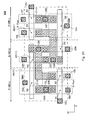
- FIG. 30 shows a layout example of a lower conductive layer of a memory cell of a CMOS-type SRAM disclosed in U.S. Pat. No. 5,930,163.
- the memory cell disclosed in U.S. Pat. No. 5,930,163 includes p-wells and n-wells which are alternately formed in the lateral direction of FIG. 30 .
- N-channel MOS transistors N 1 to N 4 are formed on the p-wells, and p-channel MOS transistors P 1 and P 2 are formed on the n-wells.
- a large number of M 1 -connection plugs 10 such as contact holes or via holes are formed so as to be connected with upper-layer interconnections (not shown).
- FIG. 31 is a partial sectional view showing a memory cell of a CMOS-type SRAM disclosed in U.S. Pat. No. 6,900,513.
- the memory cell disclosed in U.S. Pat. No. 6,900,513 includes a semiconductor substrate 2 , an isolation region 5 , active regions 6 , gate electrode interconnect layers 7 , connection plugs 10 , an intermediate connection layer 20 , local interconnections 26 and 27 , first interconnect layers M 1 , a first interlayer insulating film 51 , a second interlayer insulating film 52 , a third interlayer insulating film 53 , and a fourth interlayer insulating film 54 .
- the connection plugs 10 which are substantially concentric with each other are disposed on and below the intermediate connection layer 20 .
- the local interconnection 26 connects two active regions 6 spaced from each other, and forms a capacitance with the local interconnection 27 .
- FIG. 32 shows an equivalent circuit diagram showing a memory cell of a single-port SRAM of CMOS type.
- the SRAM memory cell includes six transistors: two p-channel MOS transistors P 1 and P 2 and four n-channel MOS transistors N 1 to N 4 .
- the six transistors are connected to a pair of bit lines (DIGT and DIGB) and a word line (WD).
- the transistors P 1 and P 2 each function as a load transistor, and the transistors N 1 and N 2 each function as a drive transistor.
- the transistors N 3 and N 4 each function as a transfer transistor.
- the transistors P 1 and N 1 constitute an inverter and the transistors P 2 and N 2 also constitute an inverter.
- the pair of inverters are connected in a crossed manner within the memory cell through a pair of intersecting lines (y 1 , y 2 ), thereby forming a flip-flop circuit serving as an information storage section that stores 1-bit information.
- a first exemplary aspect of the present invention is a semiconductor device having a regular layout region and an irregular layout region formed on one chip, the semiconductor device including: a lower conductive layer formed within a semiconductor substrate and in close proximity to the semiconductor substrate; an interlayer insulating film formed on the lower conductive layer; an upper interconnect layer formed on the interlayer insulating film; and connection plugs disposed to electrically connect the lower conductive layer and the upper interconnect layer at a substantially shortest distance.
- the lower conductive layer and the upper interconnect layer are electrically connected to each other through at least two connection plugs and an intermediate connection layer for electrically connecting the at least two connection plugs, the at least two connection plugs being disposed at an immediately above position extending from immediately above the lower conductive layer and a shift position spaced apart from the immediately above position, respectively.
- regular layout region refers to a region having a regular layout such as an SRAM memory cell.
- a region other than the regular layout region is referred to as “irregular layout region”.
- connection plugs which are disposed at positions where the connection plugs are not overlapped in plan view, and the intermediate connection layer for electrically connecting the two connection plugs are disposed between the lower conductive layer and the upper interconnect layer in the regular layout region.
- connection plugs can be reduced.
- the coverage of a barrier metal formed within the connection plugs can be improved.
- a reduction in leakage failure and a reduction in resistance of connection plugs can be realized.
- the above-mentioned effects can be exhibited by applying the above-mentioned structure to the regular layout region.
- the present invention has an advantageous effect capable of providing a semiconductor device having high reliability and improved characteristics.
- FIG. 1 is a block diagram showing a semiconductor device according to a first exemplary embodiment of the present invention
- FIG. 2A is a partial sectional view schematically showing the semiconductor device according to the first exemplary embodiment
- FIG. 2B is a partially enlarged view showing a connection plug of the semiconductor device according to the first exemplary embodiment
- FIG. 3A is a top view showing a memory cell according to the first exemplary embodiment
- FIG. 3B is a sectional view taken along the line IIIB-IIIB of FIG. 3A ;
- FIG. 3C is a sectional view taken along the line IIIC-IIIC of FIG. 3A ;
- FIG. 4A is a top view showing the memory cell according to the first exemplary embodiment
- FIG. 4B is a sectional view taken along the line IVB-IVB of FIG. 4A ;
- FIG. 4C is a sectional view taken along the line IVC-IVC of FIG. 4A ;
- FIG. 5A is a top view showing the memory cell according to the first exemplary embodiment
- FIG. 5B is a sectional view taken along the line VB-VB of FIG. 5A ;
- FIG. 5C is a sectional view taken along the line VC-VC of FIG. 5A ;
- FIG. 6 is a sectional view showing a state where layers up to a first interconnect layer of the memory cell according to the first exemplary embodiment are formed;
- FIG. 7A is a top view showing a memory cell according to a second exemplary embodiment of the present invention.
- FIG. 7B is a sectional view taken along the line VIIB-VIIB of FIG. 7A ;
- FIG. 8A is a top view showing the memory cell according to the second exemplary embodiment
- FIG. 8B is a sectional view taken along the line VIIIB-VIIIB of FIG. 8A ;
- FIG. 9 is a partially enlarged sectional view schematically showing a semiconductor device according to a third exemplary embodiment of the present invention.
- FIG. 10A is a top view showing a memory cell according to the third exemplary embodiment.
- FIG. 10B is a sectional view taken along the line XB-XB of FIG. 10A ;
- FIG. 10C is a sectional view taken along the line XC-XC of FIG. 10A ;
- FIG. 11A is a top view showing a memory cell according to a fourth exemplary embodiment of the present invention.
- FIG. 11B is a sectional view taken along the line XIB-XIB of FIG. 11A ;
- FIG. 11C is a sectional view taken along the line XIC-XIC of FIG. 11A ;
- FIG. 12A is a top view showing a memory cell according to a fifth exemplary embodiment of the present invention.
- FIG. 12B is a sectional view taken along the line XIIB-XIIB of FIG. 12A ;
- FIG. 13A is a top view showing the memory cell according to the fifth exemplary embodiment.
- FIG. 13B is a sectional view taken along the line XIIIB-XIIIB of FIG. 13A ;
- FIG. 14A is a top view showing the memory cell according to the fifth exemplary embodiment.
- FIG. 14B is a sectional view taken along the line XIVB-XIVB of FIG. 14A ;
- FIG. 15A is a top view showing the memory cell according to the fifth exemplary embodiment.
- FIG. 15B is a sectional view taken along the line XVB-XVB of FIG. 15A ;
- FIG. 15C is a sectional view taken along the line XVC-XVC of FIG. 15A ;
- FIG. 16A is a top view showing the memory cell according to the fifth exemplary embodiment.
- FIG. 16B is a sectional view taken along the line XVIB-XVIB of FIG. 16A ;
- FIG. 17A is a top view showing a memory cell according to a sixth exemplary embodiment of the present invention.
- FIG. 17B is a sectional view taken along the line XVIIB-XVIIB of FIG. 17A ;
- FIG. 18 is a block diagram showing a semiconductor device according to a seventh exemplary embodiment of the present invention.
- FIG. 19 is a partially enlarged sectional view schematically showing the semiconductor device according to the seventh exemplary embodiment.
- FIG. 20A is a top view showing a memory cell according to an eighth exemplary embodiment of the present invention.
- FIG. 20B is a sectional view taken along the line XXB-XXB of FIG. 20A ;
- FIG. 21 is a sectional view showing the memory cell according to the eighth exemplary embodiment.
- FIG. 22 is an equivalent circuit diagram showing a memory cell of a dual-port SRAM
- FIG. 23 is a top view showing a memory cell according to a ninth exemplary embodiment of the present invention.
- FIG. 24 is a top view showing the memory cell according to the ninth exemplary embodiment.
- FIG. 25 is a top view showing the memory cell according to the ninth exemplary embodiment.
- FIG. 26 is a top view showing the memory cell according to the ninth exemplary embodiment.
- FIG. 27 is a top view showing a memory cell according to a tenth exemplary embodiment of the present invention.
- FIG. 28 is a top view showing the memory cell according to the tenth exemplary embodiment.
- FIG. 29 is a top view showing the memory cell according to the tenth exemplary embodiment.
- FIG. 30 is a top view showing a memory cell disclosed in Patent Document 1;
- FIG. 31 is a sectional view showing a memory cell disclosed in Patent Document 2;
- FIG. 32 is an equivalent circuit diagram showing a memory cell of a single-port SRAM.
- FIG. 33 is a sectional view showing a state where layers up to a first interconnect layer of a memory cell according to a comparative example of the present invention are formed.
- FIG. 1 shows an example of a block diagram of a semiconductor device according to a first exemplary embodiment of the present invention.
- a semiconductor device 1 according to the first exemplary embodiment is a so-called SoC (System on a Chip) device including a logic circuit section 3 A and two SRAM sections 3 B each serving as a memory section.
- the logic circuit section 3 A and the two SRAM sections 3 B are formed on a semiconductor substrate 2 .
- Each of the SRAM sections 3 B includes a memory cell region, a decoder region, and a memory control circuit region.
- a plurality of memory cells 4 is arranged in a matrix.
- the memory cells 4 correspond to a regular layout region.
- the logic circuit section corresponds to an irregular layout region.
- FIG. 2A shows a partial sectional view schematically showing the SRAM section 3 B and the logic circuit section 3 A of the semiconductor device 1 according to the first exemplary embodiment.
- FIG. 2B shows a partially enlarged view showing a connection plug.
- the semiconductor device 1 includes the semiconductor substrate 2 , an isolation region 5 , active regions 6 , gate electrode interconnect layers 7 , side walls 8 , a silicon nitride film 9 , first interconnect layers M 1 and second interconnect layers M 2 each of which is an upper interconnect layer, first interconnect layer-connection plugs (hereinafter referred to as “M 1 -connection plug(s)”) 10 , an intermediate connection layer 20 , second interconnect layer-connection plugs (hereinafter referred to as “M 2 -connection plug(s)”) 30 , a first interlayer insulating film 51 , a second interlayer insulating film 52 , a third interlayer insulating film 53 , and a fourth interlayer insulating film 54 .
- conductive layers other than the intermediate connection layer 20 are hereinafter collectively called a lower conductive layer 11 .
- first interconnect layers M 1 and upper interconnect layers are also collectively called an upper interconnect layer.
- each of the M 1 -connection plugs 10 , the M 2 -connection plugs 30 , and the like includes a barrier metal 12 formed so as to coat the bottom surface and side wall portions of a connection hole as shown in FIG. 2B .
- a barrier metal 12 formed so as to coat the bottom surface and side wall portions of a connection hole as shown in FIG. 2B .
- titanium (Ti) or titanium nitride (TiN) can be applied as the barrier metal 12 .
- a coverage failure of the barrier metal 12 causes an increase in contact resistance and junction leakage.
- the lower conductive layer 11 and the first interconnect layer M 1 are connected to each other through the M 1 -connection plug 10 which extends immediately above the lower conductive layer 11 .
- the lower conductive layer 11 and the first interconnect layer M 1 of the SRAM section 3 B are connected, in some parts, through the M 1 -connection plug 10 , which extends immediately above the lower conductive layer 11 , in the manner as described above, and are connected, in other parts, by the following structure. That is, the lower conductive layer 11 and part of the first interconnect layer M 1 of the SRAM section 3 B are connected together with the intermediate connection layer 20 .
- the position of the M 1 -connection plug 10 formed on the intermediate connection layer 20 is shifted from a position immediately above the lower conductive layer 11 .
- the M 1 -connection plugs 10 are disposed on and below the intermediate connection layer 20 so as not to be overlapped with each other in plan view.
- the position where the connection plugs are not overlapped with each other in plan view refers to a position where the M 1 -connection plugs 10 disposed on and below the intermediate connection layer are not substantially concentric with each other when a plurality of M 1 -connection plugs 10 is disposed.
- the formation of the intermediate connection layer 20 makes it possible to reduce the aspect ratio of the M 1 -connection plugs 10 . Accordingly, the coverage of the barrier metal formed within the connection plugs can be improved. As a result, a reduction in leakage failure and a reduction in resistance of connection plugs can be realized. Additionally, the formation of the intermediate connection layer 20 makes it possible to increase the degree of freedom of design in determining the position for forming each M 1 -connection plug 10 . For example, two connection plugs formed on the intermediate connection layer 20 can be shifted in the direction in which they are spaced apart from each other, in a state where the sizes of the connection plugs in contact with the active regions 6 are minimized and adjacent connection plugs in contact with the active regions 6 are arranged in closest proximity to each other. As a result, a reduction in short-circuit failure or the like caused due to a manufacturing defect in a lithography process, for example, can be achieved. Moreover, the parasitic capacitance can be reduced.
- FIG. 3A is a top view showing a state where the lower conductive layer 11 such as the active regions 6 and the gate electrode interconnect layers 7 which are formed on the surface of the semiconductor substrate 2 , and the M 1 -connection plugs 10 are formed.
- FIG. 3B is a sectional view taken along the line IIIB-IIIB of FIG. 3A .
- FIG. 3C is a sectional view taken along the line IIIC-IIIC of FIG. 3A .
- an n-well region in which p-channel MOS transistors P 1 and P 2 are formed is located in a central area.
- a p-well region in which re-channel MOS transistors N 1 and N 3 are formed and a p-well region in which re-channel MOS transistors N 2 and N 4 are formed are located on both sides of the n-well region.
- each of the transistors P 1 and P 2 functions as a load transistor
- each of the transistors N 1 and N 2 functions as a drive transistor.
- Each of the transistors N 3 and N 4 functions as a transfer transistor.
- a pair of drive transistors and a pair of load transistors constitute a flip-flop circuit serving as an information storage section that stores 1-bit information.
- the flip-flop circuit is composed of a pair of CMOS inverters, and each of the CMOS inverters is composed of a single drive transistor N 1 (N 2 ) and a single load transistor P 1 (P 2 ).
- the six transistors constituting the memory cell are formed in the active region 6 which is a diffusion region surrounded by the isolation region 5 that is formed on the semiconductor substrate 2 made of monocrystalline silicon.
- the active region 6 includes an n-type active region 6 N and a p-type active region 6 P.
- Each transistor includes a source/drain region formed in the active region, a gate insulating film (not shown) formed on the surface of the active region, and the gate electrode interconnect layer 7 formed on the gate insulating film.
- the gate electrode interconnect layer 7 has a stacked structure of, for example, a doped polycrystalline silicon film and a refractory metal silicide film (a titanium silicide film, a cobalt silicide film, a nickel silicide film, or the like), or a metal gate structure.
- a refractory metal silicide film a titanium silicide film, a cobalt silicide film, a nickel silicide film, or the like
- a metal gate structure On the side walls of the gate electrode interconnect layer 7 , the side walls 8 are formed (see FIG. 2A ). Additionally, at the upper portion of the gate electrode interconnect layer 7 , a silicon nitride film (not shown) is formed. Note that a metal silicide layer may be formed on the silicon surface of the active regions 6 N and 6 P.
- the first interlayer insulating film 51 is formed on the silicon nitride film 9 .
- the first interlayer insulating film 51 has connection holes 81 formed through the first interlayer insulating film 51 from the surface thereof to reach the active regions 6 N and 6 P.
- M 1 -connection plugs 10 a , 10 b , and 10 c are disposed in the connection holes 81 .
- the first interlayer insulating film 51 has the connection holes 81 formed through the first interlayer insulating film 51 from the surface thereof to reach the active regions 6 N and 6 P, and M 1 -connection plugs 10 d and 10 e are disposed in the connection holes 81 .
- the M 1 -connection plugs 10 may be applied with tungsten, for example.
- the barrier metal 12 as shown in FIG. 2B is formed within the connection holes 81 .
- the first interlayer insulating film 51 has connection holes 82 penetrating through the surface of the gate electrode interconnect layer 7 , and the M 1 -connection plugs 10 are disposed in the connection holes 82 in a similar manner as described above (see FIG. 2A ).
- FIG. 4A is a top view showing a state where the intermediate connection layers 20 are formed for the structure shown in FIG. 3A .
- FIG. 4B is a sectional view taken along the line IVB-IVB of FIG. 4A .
- FIG. 4C is a sectional view taken along the line IVC-IVC of FIG. 4A .
- the intermediate connection layers 20 are formed immediately above the M 1 -connection plugs 10 a , 10 b , 10 c , and 10 f (see FIG. 3A ) so as to coat the M 1 -connection plugs (see FIG. 4A ). Specifically, intermediate connection layers 20 a , 20 b , 20 c , and 20 f are formed immediately above the M 1 -connection plugs 10 a , 10 b , 10 c , and 10 f , respectively.
- the intermediate connection layers 20 b and 20 c are formed so that the intermediate connection layers 20 b and 20 c are aligned with the M 1 -connection plugs 10 b and 10 c , respectively, in the layout, on the side where the M 1 -connection plugs 10 b and 10 c formed below the intermediate connection layers 20 b and 20 c face each other.
- the intermediate connection layers 20 b and 20 c are coated so as not to project from the M 1 -connection plugs 10 b and 10 c on the side where the M 1 -connection plugs 10 b and 10 c formed therebelow face each other, and so as not to expose the M 1 -connection plugs 10 b and 10 c .
- a distance between the M 1 -connection plug 10 b and the M 1 -connection plug 10 c is substantially the same as a distance between the intermediate connection layer 20 b and the intermediate connection layer 20 c.
- Each of the intermediate connection layers 20 a and 20 c has an extended region which extends rightward in FIG. 4A
- each of the intermediate connection layers 20 b and 20 f has an extended region which extends leftward in FIG. 4A
- the intermediate connection layer 20 may have a thickness smaller than that of the upper interconnect layer such as the first interconnect layer M 1 . Accordingly, the intermediate connection layer 20 can be formed not only by a typical Cu-Damascene Process, but also by a sputtering method, a CVD method, and the like.
- the material is not particularly limited, and metals such as tungsten, titanium nitride (TiN), and copper, or conductive films equivalent to metals can be applied, for example. From the viewpoint of reducing the resistance, low-resistance conductive films may preferably be used.
- the thickness of the intermediate connection layer 20 is not particularly limited, but may be preferably reduced without sacrificing superior film formation characteristics, in view of the pattern accuracy. Though the thickness is determined depending on the material to be used and the required resistance characteristics, the thickness may be about 1 ⁇ 2 to 1 ⁇ 4 of that of the first interconnect layer M 1 , for example.
- the intermediate connection layer 20 is formed only immediately above the four M 1 -connection plugs 10 a , 10 b , 10 c , and 10 f among the M 1 -connection plugs 10 of the memory cell region.
- This embodiment is illustrative only, and the positions and the number of the intermediate connection layers 20 may be arbitrarily determined.
- FIG. 5A is a top view showing a state where there are formed the second interlayer insulating film 52 , connection holes 83 penetrating from the surface of the second interlayer insulating film 52 to the surface of the intermediate connection layer 20 or the M 1 -connection plugs 10 which is formed in the first interlayer insulating film 51 , and the M 1 -connection plugs 10 which are disposed in the connection holes 83 .
- FIG. 5B is a sectional view taken along the line VB-VB of FIG. 5A .
- FIG. 5C is a sectional view taken along the line VC-VC of FIG. 5A .
- an M 1 -connection plug 10 g is disposed on the intermediate connection layer 20 a so as not to be overlapped in plan view with the M-connection plug 10 a which is disposed below the intermediate connection layer 20 a .
- the position of the M 1 -connection plug 10 g which is formed on the intermediate connection layer 20 a , is shifted rightward in FIG. 5B with respect to the position where the M 1 -connection plug 10 a is formed below the intermediate connection layer 20 a .
- an M 1 -connection plug 10 h is disposed on the extended region of the intermediate connection layer 20 b which extends leftward in FIG.
- an M 1 -connection plug 10 i formed on the intermediate connection layer 20 c is disposed on the extended region which extends rightward in FIG. 5B , so as not to be overlapped in plan view with the M 1 -connection plug 10 c which is disposed below the intermediate connection layer 20 c .
- connection plugs are disposed so as not to be overlapped in plan view” refers to the state where the M 1 -connection plugs disposed on and below the intermediate connection layer (e.g., M 1 -connection plugs 10 a and 10 g , 10 b and 10 h , and 10 c and 10 i ) are not substantially concentric with each other.
- the shift amount thereof is not particularly limited.
- M 1 -connection plugs 10 j and 10 k are disposed immediately above the M 1 -connection plugs 10 d and 10 e , respectively, without involving the intermediate connection layer.
- FIG. 6 is a sectional view showing a state where the first interconnect layers M 1 are further formed on the second interlayer insulating film 52 in a region corresponding to the sectional view of FIG. 5B .
- a pattern of a first interconnect layer M 1 a is formed so as to electrically connect the M 1 -connection plugs 10 g and 10 h .
- a pattern of a first interconnect layer M 1 b is formed on the M 1 -connection plug 10 i .
- a distance between the M 1 -connection plug 10 h and 10 i is represented by D 1 ; a distance between the first interconnect layers M 1 a and M 1 b is represented by D 2 ; and a distance between the M 1 -connection plugs 10 b and 10 c is represented by D 3 .
- the formation of the intermediate connection layers 20 b and 20 c makes it possible to increase the distance D 1 between the M 1 -connection plugs 10 h and 10 i while allowing the M 1 -connection plugs 10 b and 10 c , which are positioned below the intermediate connection layers, to be disposed at the immediately above positions extending from immediately above the active regions 6 . This also contributes to an increase in the distance D 2 between the first interconnect layers M 1 a and M 1 b.
- FIG. 33 is a sectional view showing a case where the intermediate connection layer is not formed at positions corresponding to those of the FIG. 6 .
- a distance between M 1 -connection plugs 110 b and 110 c is represented by D 3 in the same manner as in the first exemplary embodiment.
- a distance between the first interconnect layers M 101 a and M 101 b is represented by D 4 . Since the intermediate connection layer is not formed, the distance D 4 is at least the same as the distance D 3 or shorter than the distance D 3 .
- the distance D 2 between the patterns of the first interconnect layers M 1 a and M 1 b can be increased in a state where the sizes of the connection plugs in contact with the active regions 6 are minimized and adjacent connection plugs in contact with the active region 6 are arranged in closest proximity to each other.
- distance D 4 distance between the M 1 -interconnect layers M 101 a and M 101 b of the comparative example
- D 2 distance between the M 1 -connection layers M 1 a and M 1 b of the first exemplary embodiment
- the intermediate connection layer 20 is formed to change the connection between the M 1 -connection plugs, which results in a reduction of the aspect ratio of the M 1 -connection plugs.
- (an aspect ratio h2/r1 of the M 1 -connection plugs according to the comparative example)>(an aspect ratio h1/r1 of the M 1 -connection plugs according to an exemplary embodiment of the present invention) is satisfied. Accordingly, a taper angle obtained by processing the connection holes and the coverage of the barrier metal which forms the M 1 -connection plugs can be improved. As a result, a suppression of a leakage failure and a reduction in connection resistance can be realized.
- the positions to be connected with the upper interconnect layer can be adjusted without changing the layout of the lower conductive layers of the transistors in which the area of the memory cell 4 is reduced. This contributes to an increase in degree of freedom of design.
- connection holes can be widened and the limitations on the shape and layout of the upper interconnect layer by the layout of the lower layers can be alleviated.
- the deterioration in yield and operation margin due to pattern defects caused by lithography or the like, a parasitic capacitance, noise, signal interference, or the like due to the layout can be reduced or improved, while achieving the miniaturization of the SRAM.
- connection holes 81 and 82 are formed at the positions where the intermediate connection layer 20 is not formed, after the formation of the first interlayer insulating film 51 , and the M 1 -connection plugs 10 (e.g., 10 a to 10 f ) are disposed. Then, after the formation of the second interlayer insulating film 52 , the connection holes 83 are formed and the M 1 -connection plugs 10 (e.g., 10 g to 10 i ) are disposed.
- connection holes penetrating from the surface of the second interlayer insulating film 52 to the lower conductive layer 11 which is formed below the first interlayer insulating film 51 are formed, and then the M 1 -connection plugs 10 are disposed.
- FIG. 7A is a top view showing a memory cell 204 in a state where the lower conductive layer 11 , such as the active regions 6 and the gate electrode interconnect layers 7 formed on the surface of the semiconductor substrate 2 , and the M 1 -connection plugs 10 are formed.
- FIG. 7B is a sectional view taken along the line VIIB-VIIB of FIG. 7A .
- the first interlayer insulating film 51 has the connection holes 81 penetrating from the surface thereof to the active regions 6 N and 6 P.
- the M 1 -connection plugs 10 a , 10 b , 10 c , and 10 f are disposed in the connection holes 81 .
- the first interlayer insulating film 51 in the other regions has no connection hole as shown in FIG. 7B , unlike the first exemplary embodiment.
- FIG. 8A is a top view showing the memory cell 204 in a state where the second interlayer insulating film 52 is formed and the M 1 -connection plugs 10 are disposed on the surface of the second interlayer insulating film 52 .
- FIG. 8B is a sectional view taken along the line VIIIB-VIIIB of FIG. 8A .
- the intermediate connection layers 20 are formed immediately above the M 1 -connection plugs 10 a , 10 b , 10 c , and 10 f (see FIG. 3A ) so as to coat the M 1 -connection plugs.
- the corresponding M 1 -connection plug 10 g , 10 h , and 10 i are formed on the intermediate connection layers 20 a , 20 b , and 20 c , respectively, in a similar manner as in the first exemplary embodiment. Meanwhile, as shown in FIG.
- M 1 -connection plugs 10 m and 10 n are formed in connection holes 84 penetrating from the surface of the second interlayer insulating film 52 to the active regions 6 which are formed below the first interlayer insulating film 51 .
- the same effects as those of the first exemplary embodiment can be obtained by forming the intermediate connection layer 20 . Further, only the particular contacts in the memory cell section are formed in a minimum size, and the other contacts having a design margin in the memory cell are formed with a size that is common to the logic circuit section which has a size greater than the minimum size. As a result, the production yield can be improved.
- the basic structure of a semiconductor device according to a third exemplary embodiment of the present invention is similar to that of the first exemplary embodiment, except for the following. That is, in the semiconductor device 1 according to the first exemplary embodiment, the intermediate connection layer 20 is formed only in the region in which the arrangement positions of the M 1 -connection plugs 10 are intended to be shifted from the immediately above positions extending from immediately above the lower conductive layer 11 . Meanwhile, in the semiconductor device according to the third exemplary embodiment, the intermediate connection layer 20 is formed at all the positions where the M 1 -connection plugs 10 are disposed in a gap between the first interlayer insulating film 51 and the second interlayer insulating film 52 .
- FIG. 9 is a partial sectional view schematically showing the SRAM section 3 B and the logic circuit section 3 A of a semiconductor device 301 according to the third exemplary embodiment.
- the lower conductive layer and the first interconnect layers M 1 are connected together through the M 1 -connection plugs 10 which extend immediately above the lower conductive layer.
- the intermediate connection layer 20 is disposed between each of the M 1 -connection plugs 10 which are disposed in the connection holes formed in the first interlayer insulating film 51 and each of the M 1 -connection plugs 10 which are disposed in the connection holes formed in the second interlayer insulating film 52 .
- the intermediate connection layer 20 has a rectangular pattern which has a size equal to or larger than that of an exposed portion of each connection plug so as to coat the M 1 -connection plugs 10 formed on the surface of the first interlayer insulating film 51 .
- the intermediate connection layer 20 is formed in the region in which the M 1 -connection plugs 10 are intended to be shifted from the immediately above positions extending immediately above the lower conductive layer 11 , and the following structure is also included. That is, as in the logic circuit section 3 A according to the third exemplary embodiment, the SRAM section 3 B includes the intermediate connection layer 20 for connecting each of the M 1 -connection plugs 10 which are disposed in the connection holes formed in the first interlayer insulating film 51 and each of the M 1 -connection plugs 10 which are disposed in the connection holes formed in the second interlayer insulating film 52 .
- the M 1 -connection plugs 10 are disposed so as to be overlapped with each other in plan view.
- FIG. 10A is a top view showing a state where layers up to the intermediate connection layer 20 are formed on the semiconductor substrate 2 .
- FIG. 10B is a sectional view taken along the line XB-XB of FIG. 10A .
- FIG. 10C is a sectional view taken along the line XC-XC of FIG. 10A .
- the intermediate connection layers 20 are formed immediately above the M 1 -connection plugs 10 a , 10 b , 10 c , and 10 f (see FIG. 3A ) so as to coat the M 1 -connection plugs.
- the intermediate connection layers 20 a , 20 b , 20 c , and 20 f are formed immediately above the M 1 -connection plugs 10 a , 10 b , 10 c , and 10 f , respectively.
- the patterns of the intermediate connection layers 20 a , 20 b , 20 c , and 20 f are formed to have a size greater than that of an exposed area of each M 1 -connection plug 10 formed therebelow.
- the patterns of at least the intermediate connection layers 20 b and 20 c among the intermediate connection layers are formed so that the intermediate connection layers 20 b and 20 c are aligned with the M 1 -connection plugs 10 b and 10 c , respectively, in the layout, on the side where the M 1 -connection plugs 10 b and 10 c formed below the intermediate connection layers 20 b and 20 c face each other.
- each of the intermediate connection layers 20 a and 20 c has an extended region which extends rightward in FIG. 4B
- each of the intermediate connection layers 20 b and 20 f has an extended region which extends leftward in FIG. 4A .
- the intermediate connection layers 20 have a size equal to or larger than that of the M 1 -connection plugs 10 so as to coat the M 1 -connection plugs 10 which are exposed to the surface of the first interlayer insulating film 51 .
- intermediate connection layers 20 d and 20 e which have a size larger than that of the corresponding M 1 -connection plugs 10 are formed on the M 1 -connection plugs 10 d and 10 e shown in FIG. 10C , respectively, so as to coat the region exposed to the surface of the first interlayer insulating film 51 .
- the same effects as those of the first exemplary embodiment can be obtained by forming the intermediate connection layer 20 .
- the intermediate connection layer is formed at the positions to be connected with the M 1 -connection plugs which are formed in the first interlayer insulating film 51 and the second interlayer insulating film 52 .
- the sizes of the connection plugs formed on and below the intermediate connection layer can be changed, thereby making it possible to improve the layout design and the aspect ratio depending on the required characteristics.
- defects due to displacement of the connection holes formed in each layer can be reduced.
- the basic structure of a semiconductor device according to a fourth exemplary embodiment of the present invention is similar to that of the first exemplary embodiment, except for the following. That is, in the semiconductor device 1 according to the first exemplary embodiment, the intermediate connection layer 20 is formed only in the region in which the arrangement positions of the M 1 -connection plugs 10 are intended to be shifted from the immediately above positions extending from immediately above the lower conductive layer 11 . Meanwhile, in the semiconductor device according to the fourth exemplary embodiment, the intermediate connection layers 20 are formed at the above-mentioned positions as well as arbitrary positions for disposing the M 1 -connection plugs 10 in a gap between the first interlayer insulating film 51 and the second interlayer insulating film 52 .
- FIG. 11A is a top view showing a memory cell 404 in a state where layers up to the intermediate connection layers 20 are formed on the semiconductor substrate 2 .
- FIG. 11B is a sectional view taken along the line XIB-XIB of FIG. 11A .
- FIG. 11C is a sectional view taken along the line XIC-XIC of FIG. 11A .
- the intermediate connection layers 20 are formed immediately above the M 1 -connection plugs 10 a , 10 b , 10 c , and 10 f (see FIG. 3A ) so as to coat the M 1 -connection plugs (see FIG. 11A ).
- the intermediate connection layers 20 a , 20 b , 20 c , and 20 f are formed immediately above the M 1 -connection plugs 10 a , 10 b , 10 c , and 10 f , respectively.
- the intermediate connection layers 20 are formed.
- the intermediate connection layers 20 having a size equal to or larger than that of the M 1 -connection plugs 10 may be formed so as to coat the M 1 -connection plugs 10 which are exposed to the surface of the first interlayer insulating film 51 .
- the intermediate connection layers 20 having an extended region, such as the intermediate connection layers 20 a , 20 b , 20 c , and 20 f may be formed.
- the arrangement positions of the intermediate connection layers 20 can be arbitrarily set, which significantly increases the degree of freedom of design.
- the intermediate connection layers 20 can be formed in a region in which small-size connection plugs are formed, a region in which there arises a problem of parasitic capacitance, or a region in which connection plugs are adjacent to each other.
- the connection plugs can be directly connected together without forming any intermediate connection layer, or the one connection plug can be disposed from the lower conductive layer to the surface of the second interlayer insulating film.
- the semiconductor device can be designed in the optimum state, depending on specific usage, needs, and specifications.
- the basic structure of a semiconductor device according to a fifth exemplary embodiment of the present invention is similar to that of the first exemplary embodiment, except for the following. That is, in the semiconductor device 1 according to the first exemplary embodiment, the M 1 -connection plugs 10 to be connected to the lower conductive layer are disposed at each connecting location. Meanwhile, in the semiconductor device 1 according to the fifth exemplary embodiment, some M 1 -connection plugs 10 to be connected to the lower conductive layer are used as common connection plugs.
- FIG. 12A shows a top view showing a memory cell 504 in a state where layers up to the first interlayer insulating film 51 and the M 1 -connection plugs 10 are formed on the semiconductor substrate 2 .
- FIG. 12B is a sectional view taken along the line XIIB-XIIB of FIG. 12A .
- the M 1 -connection plug 10 b of the first exemplary embodiment shown in FIG. 3A is integrated with the M 1 -connection plug 10 which is located adjacent to the M 1 -connection plug 10 b on the lower side of FIG. 3A , thereby forming a common connection plug 10 p (see FIG. 12B ).
- the M 1 -connection plug 10 f of the first exemplary embodiment shown in FIG. 3A is integrated with the M 1 -connection plug 10 which is located adjacent to the M 1 -connection plug 10 f on the upper side of FIG. 3A , thereby forming a common connection plug 10 q.
- FIG. 13A is a top view showing a state where the intermediate connection layers 20 are further formed in the structure shown in FIG. 12A .
- FIG. 13B is a sectional view taken along the line XIIIB-XIIIB of FIG. 13A .
- the arrangement positions and shapes of the intermediate connection layers 20 a , 20 b , 20 c , and 20 f are similar to those of the first exemplary embodiment.
- the intermediate connection layer 20 is formed so as to be in contact with a certain region of the upper surface of the M 1 -connection plug 10 p (see FIGS. 13A and 13B ).
- the intermediate connection layer 20 is formed so as to be in contact with a certain region of the upper surface of the M 1 -connection plug 10 q.
- FIG. 14A is a top view showing a state where the second interlayer insulating film 52 is formed and the M 1 -connection plugs 10 are formed in the connection holes of the second interlayer insulating film 52 .
- FIG. 14B is a sectional view taken along the line XIVB-XIVB of FIG. 14A .
- FIG. 15A is a top view showing a state where layers up to the first interconnect layers M 1 are formed.
- FIG. 15B is a sectional view taken along the line XVB-XVB of FIG. 15A
- FIG. 15C is a sectional view taken along the line XVC-XVC of FIG. 15A .
- FIG. 16A is a top view showing a state where layers up to the second interconnect layers M 2 are formed
- FIG. 16B is a sectional view taken along the line XVIB-XVIB of FIG. 16A .
- the second interlayer insulating film 52 is formed so as to coat the upper layer of the M 1 -connection plugs 10 which are exposed to the surface of the first interlayer insulating film 51 and to coat the intermediate connection layer 20 formed on a portion of the upper layer (see FIG. 14B ).
- the second interlayer insulating film 52 has connection holes for connecting the M 1 -connection plugs 10 of the first interlayer insulating film 51 or the intermediate connection layer 20 formed above M 1 -connection plugs 10 .
- the M 1 -connection plugs 10 are formed in the connection holes. Specifically, as shown in FIG.
- the M 1 -connection plug 10 p which is a common connection plug formed in the first interlayer insulating film 51
- the M 1 -connection plug 10 h which is formed in the second interlayer insulating film 52
- the M 1 -connection plug 10 e which is a common connection plug formed in the first interlayer insulating film 51
- the M 1 -connection plug 10 k which is formed in the second interlayer insulating film 52
- the first interconnect layers M 1 are formed on the M 1 -connection plugs 10 which are exposed to the surface of the second interlayer insulating film 52 (see FIG. 15A ).
- the pattern of the first interconnect layer M 1 a is formed on the M 1 -connection plugs 10 g and 10 h , which are formed in the second interlayer insulating film 52 , so as to coat both the M 1 -connection plugs 10 g and 10 h .
- the pattern of the first interconnect layer M 1 b is formed on the M 1 -connection plug 10 i , which is formed in the second interlayer insulating film 52 , so as to coat the M 1 -connection plug 10 i .
- FIG. 15B the pattern of the first interconnect layer M 1 a is formed on the M 1 -connection plugs 10 g and 10 h , which are formed in the second interlayer insulating film 52 , so as to coat both the M 1 -connection plugs 10 g and 10 h .
- first interconnect layers M 1 c and M 1 d are respectively formed on the M 1 -connection plugs 10 j and 10 k , which are formed in the second interlayer insulating film 52 , so as to coat the M 1 -connection plugs 10 j and 10 k , respectively.
- These patterns of the first interconnect layers M 1 are formed in a rectangular shape having no bent portion, and the first interconnect layers M 1 a and M 1 b are spaced apart due to the layout of the lower layer.
- the third interlayer insulating film 53 is formed on the first interconnect layers M 1 , and the M 2 -connection plug 30 is disposed in a connection hole 85 which is formed in the third interlayer insulating film 53 (see FIG. 16B ). Further, the second interconnect layers M 2 are formed so as to coat the M 2 -connection plug 30 which is exposed to the upper surface of the third interlayer insulating film 53 (see FIGS. 16A and 16B ). In the example shown in FIG. 16B , a second interconnect layer M 2 b is formed on the M 2 -connection plug 30 , and part of the second interconnect layer M 2 b is disposed so as to face the first interconnect layer M 1 d through the M 2 -connection plug 30 . Additionally, at a position adjacent to the second interconnect layer M 2 b , another pattern of a second interconnect layer M 2 a is formed.
- the same effects as those of the first exemplary embodiment can be obtained by forming the intermediate connection layer 20 .
- the combination of the common connection plug and the intermediate connection layer 20 can effectively enhance the effect of increasing the degree of freedom of design for positioning the upper interconnect layer and the M 1 -connection plugs 10 , without any limitations on the layout of the lower conductive layer.
- the basic structure of a semiconductor device according to a sixth exemplary embodiment of the present invention is similar to that of the second exemplary embodiment, except for the following. That is, in the semiconductor device according to the second exemplary embodiment, one M 1 -connection plug is connected to each of the upper surface and the lower surface of a single intermediate connection layer 20 . Meanwhile, in the semiconductor device according to the sixth exemplary embodiment, two M 1 -connection plugs 10 are disposed below a single intermediate connection layer 20 . As a result, the local interconnect function can be added to the intermediate connection layer 20 .
- FIG. 17A is a top view showing a memory cell 604 in a state where layers up to the second interlayer insulating film 52 and the M 1 -connection plugs 10 , which are formed in the second interlayer insulating film 52 , are formed.
- FIG. 17B is a sectional view taken along the line XVIIB-XVIIB of FIG. 17A .
- an intermediate connection layer 20 g is formed so as to coat two M 1 -connection plugs 10 t and 10 u which are formed in the first interlayer insulating film 51 .
- An M 1 -connection plug 10 v is formed on the intermediate connection layer 20 g .
- an active region 6 Pa and the first interconnect layer M 1 are connected together through the M 1 -connection plug 10 u , the intermediate connection layer 20 g , and the M 1 -connection plug 10 v . Further, as shown in FIG.
- the gate electrode interconnect layer 7 and the first interconnect layer M 1 are connected together through the M 1 -connection plug 10 t , the intermediate connection layer 20 g , and the M 1 -connection plug 10 v . Furthermore, an active region 6 Pb is connected to the first interconnect layer M 1 (not shown) through an M 1 -connection plug 10 w.
- the same effects as those of the first exemplary embodiment can be obtained by forming the intermediate connection layer 20 .
- the local interconnect function for connecting the lower conductive layers 11 is added to the intermediate connection layer 20 , thereby making it possible to increase the degree of freedom of design of the interconnect structure, without any limitations on the layout of the lower interconnect layer.
- the local interconnection according to the sixth exemplary embodiment is illustrated by way of example only, and intersecting lines of a flip-flop circuit may be formed by the intermediate connection layer, for example.
- the sixth exemplary embodiment has been described as an example where the M 1 -connection plugs 10 to be connected to the first interconnect layer M 1 are formed on the intermediate connection layer 20 which is a local interconnect layer, an intermediate connection layer having only the local interconnect function may be formed.
- the number of M 1 -connection plugs 10 to be connected to the intermediate connection layer is not particularly limited.
- a plurality of M 1 -connection plugs 10 may be disposed on the upper surface of the intermediate connection layer, and may be connected to the same or different first interconnect layer M 1 .
- FIG. 18 shows an example of a block diagram of a semiconductor device according to the seventh exemplary embodiment.
- a logic circuit section 3 A, an SRAM section 3 B, and a DRAM (Dynamic Random Access Memory) section 3 C are mixed.
- the SRAM section 3 B and the DRAM section 3 C are memory sections.
- FIG. 19 is a partially sectional view schematically showing the logic circuit section 3 A, the SRAM section 3 B, and the DRAM section 3 C of the semiconductor device 701 according to the seventh exemplary embodiment.
- the semiconductor device 701 includes a bit-line-connection plug 15 , an MIM-connection plug 16 , a bit line 25 , an MIM (Metal-Insulator-Metal) capacitance 40 , a fourth interlayer insulating film 54 , and a fifth interlayer insulating film 55 , in addition to the components of the first exemplary embodiment shown in FIG. 2A .
- the MIM capacitor 40 is formed in the DRAM section 3 C, and includes a lower-layer metal 41 , a capacitor insulating film 42 , and an upper-layer metal 43 . Note that, for convenience of explanation, illustration of the upper interconnect layer including the second interconnect layer M 2 is omitted.
- the intermediate connection layer 20 is formed on the first interlayer insulating film 51 .
- the first interconnect layers M 1 are formed on the fourth interlayer insulating film 54 .
- the bit line 25 which is formed by the same material and the same process as the intermediate connection layer 20 , is disposed immediately above the first interlayer insulating film 51 of the DRAM section 3 C.
- the bit line 25 is electrically connected to the active region 6 through the bit-line-connection plug 15 .
- a connection hole penetrating from the surface of the second interlayer insulating film 52 to the surface of the active region 6 is formed.
- the MIM-connection plug 16 is disposed in the connection hole.
- the third interlayer insulating film 53 has an opening 86 for forming the MIM capacitor 40 .
- the opening 86 reaches the surface of the second interlayer insulating film 52 , and is formed so as to be overlapped with the position at which the MIM-connection plug 16 is formed.
- the lower-layer metal 41 of the MIM capacitor 40 is formed so as to coat a bottom portion and a side wall portion of the opening 86 .
- the capacitor insulating film 42 is stacked so as to coat the upper layer of the lower-layer metal 41 and a portion of the surface of the third interlayer insulating film 53 in the vicinity of the opening 86 .
- the upper-layer metal 43 is stacked so as to coat the capacitor insulating film 42 .
- the fourth interlayer insulating film 54 is formed so as to coat the MIM capacitor 40 . Further, the first interconnect layers M 1 are formed on the fourth interlayer insulating film 54 . The first interconnect layers M 1 and the lower conductive layer (e.g., the active regions 6 and the gate electrode interconnect layers 7 ) are connected to each other through the M 1 -connection plugs 10 which are disposed in the connection holes formed in each interlayer insulating film.
- the lower conductive layer 11 and the M 1 -connection plugs 10 are connected to each other through the M 1 -connection plugs 10 which are formed immediately above positions so as to extend from immediately above the lower conductive layer 11 , without involving the intermediate connection layer 20 .
- the intermediate connection layer 20 may be formed at a position where the M 1 -connection plugs are in contact with each other between the interlayer insulating films.
- the intermediate connection layer 20 is formed between the first interlayer insulating film 51 and the second interlayer insulating film 52 .
- the intermediate connection layer 20 may be formed between the second interlayer insulating film 52 and the third interlayer insulating film 53 , or between the third interlayer insulating film 53 and the fourth interlayer insulating film 54 , for example.
- the description has been given of the case where the first interconnect layers M 1 are formed at positions in the upper layer of the fourth interlayer insulating film 54 this is merely an example and the first interconnect layers M 1 may be formed in the third interlayer insulating film or in the upper layer of the fourth interlayer insulating film 54 .
- the intermediate connection layer 20 may be formed of multiple layers.
- the intermediate connection layer 20 may be formed between the first interlayer insulating film 51 and the second interlayer insulating film 52 , or between the third interlayer insulating film 53 and the fourth interlayer insulating film 54 .
- the upper-layer metal 43 of the MIM capacitor 40 may be formed by the same material and the same process as the intermediate connection layer.
- the same effects as those of the first exemplary embodiment can be obtained by forming the intermediate connection layer 20 .
- the intermediate connection layer 20 may be shared by the bit line 25 , the upper-layer metal 43 of the MIM capacitor 40 , or the like.
- the efficiency of the manufacturing process can be enhanced.
- the bit line 25 is illustrative only, and a word line may be formed at the position of the bit line 25 and may be shared by the intermediate connection layer.
- the first interconnect layers M 1 are formed on the third interlayer insulating film 53 . Additionally, in the eighth exemplary embodiment, an MIM capacitor 840 is formed on the second interlayer insulating film 52 .
- FIG. 20A is a top view showing a memory cell 804 in a state where the second interlayer insulating film 52 and the M 1 -connection plugs 10 which are formed in the second interlayer insulating film 52 are formed.
- FIG. 20B is a sectional view taken along the line XXB-XXB of FIG. 20A .
- FIG. 21 is a sectional view showing a state where the MIM capacitor 840 , the third interlayer insulating film 53 , the M 1 -connection plugs 10 , and the first interconnect layers M 1 are further formed in the upper layer shown in FIG. 20B .
- an intermediate connection layer 20 h is formed on the two M 1 -connection plugs 10 a and 10 b which are formed in the first interlayer insulating film 51 .
- An M 1 -connection plug 10 x is formed on the intermediate connection layer 20 h .
- the active region 6 Pa and the first interconnect layer M 1 (not shown) are connected together through the M 1 -connection plug 10 b , the intermediate connection layer 20 h , and the M 1 -connection plug 10 x . Further, as shown in FIG.
- the active region 6 N and the first interconnect layer M 1 are connected together through the M 1 -connection plug 10 a , the intermediate connection layer 20 h , and the M 1 -connection plug 10 x . Furthermore, the active region 6 Pb and the first interconnect layer M 1 (not shown) are connected together through the M 1 -connection plug 10 c , an intermediate connection layer 20 i , and an M 1 -connection plug 10 y.
- the MIM capacitor 840 is formed on the second interlayer insulating film 52 .
- the MIM capacitor 840 includes a lower-layer metal 841 , a capacitor insulating film 842 , and an upper-layer metal 843 .
- an M 1 -connection plug 10 z is disposed in a connection hole penetrating from the surface of the third interlayer insulating film 53 to the surface of the lower-layer metal 841 .
- an M 1 -connection plug 10 z 1 is disposed in a connection hole penetrating from the surface of the third interlayer insulating film 53 to the surface of the upper-layer metal 843 .
- a first interconnect layer M 1 e is formed on the M 1 -connection plug 10 z which is exposed to the surface of the third interlayer insulating film 53 .
- a first interconnect layer M 1 f is formed on the M 1 -connection plug 10 z 1 which is exposed to the surface of the third interlayer insulating film 53 .
- the same effects as those of the first exemplary embodiment can be obtained by forming the intermediate connection layer 20 .
- the local interconnect function for connecting the lower conductive layers is added to the intermediate connection layer 20 , thereby making it possible to increase the degree of freedom of design of the interconnect structure, without any limitations on the layout of the lower interconnect layer.
- the degree of freedom of arrangement positions of the M 1 -conection plugs 10 is increased by applying the intermediate connection layer 20 .
- functional elements such as the MIM capacitor can be mounted, for example, so as to improve the SER (Soft Error Rates) resistance while maintaining the layout of the lower conductive layer 11 .
- FIG. 22 is an equivalent circuit diagram showing a memory cell of the CMOS dual-port SRAM.
- a memory cell 904 of the SRAM includes eight transistors: two p-channel MOS transistors P 3 and P 4 and six n-channel MOS transistors N 5 , N 6 , and A 1 to A 4 .
- the memory cell 904 has two ports for inputting and outputting data.
- An A-port is composed of the transistors A 1 and A 2
- a B-port is composed of the transistors A 3 and A 4 .
- the A-port composed of the transistors A 1 and A 2 is connected with a pair of bit lines DBA and DTA and a word line WLA.
- the B-port composed of the transistors A 3 and A 4 is connected with a pair of bit lines DBB and DTB and a word line WLB. Note that the transistors P 3 and P 4 each function as a load transistor, like the transistors P 1 and P 2 .
- the transistors N 5 and N 6 each function as a drive transistor.
- FIG. 23 is a top view showing a base layer including the active regions 6 , which are formed on the surface of the semiconductor substrate 2 , the lower conductive layer 11 such as the gate electrode interconnect layers 7 , and the M 1 -connection plugs 10 .
- an n-well region in which the p-channel MOS transistors P 3 and P 4 are formed is located in a central area, and a p-well region in which the n-channel MOS transistors N 5 , A 1 , and A 2 are formed and a p-well region in which the n-channel MOS transistors N 6 , A 3 , and A 4 are formed are located on both sides of the n-well region.
- the eight transistors constituting the memory cell 904 are manufactured by using materials and a manufacturing method similar to those of the first exemplary embodiment, for example. As shown in FIG. 23 , M 1 -connection plugs 10 B to 10 K are disposed in connection holes penetrating from the surface of the first interlayer insulating film 51 (not shown) (see FIG. 3A ) to the surface of the active regions 6 N and 6 P or to the surface of the gate electrode interconnect layers 7 .
- FIG. 24 is a top view showing a state where intermediate connection layers 20 A to 20 D and the M 1 -connection plugs 10 formed thereon are further formed in the structure shown in FIG. 23 .
- the intermediate connection layer 20 A extends in the Y-direction of FIG. 24 so as to coat the M 1 -connection plugs 10 B and 10 C which are exposed to the surface of the first interlayer insulating film 51 (not shown).
- the intermediate connection layer 20 B is formed so as to coat the M 1 -connection plugs 10 D, 10 G, and 10 H.
- the intermediate connection layer 20 B includes a region extending in the Y-direction of FIG.
- the intermediate connection layer 20 C is formed so as to coat the M 1 -connection plugs 10 E, 10 F, and 10 I.
- the intermediate connection layer 20 C includes a region extending in the Y-direction so as to coat the M 1 -connection plugs 10 E and 10 F, a region extending in the Y-direction so as to coat the M 1 -connection plug 10 I, and a region extending in the X-direction from the vicinity of a central portion between the M 1 -connection plugs 10 E and 10 F so as to connect these regions.
- the intermediate connection layer 20 D extends in the Y-direction so as to coat the M 1 -connection plugs 10 J and 10 K.
- the intermediate connection layer 20 B forms a connection line Y 4 between an intersecting line Y 2 of the flip-flop circuit and the transistor A 2 shown in FIG. 22 .
- the intermediate connection layer 20 C forms a connection line Y 5 between an intersecting line Y 1 of the flip-flop and the transistor A 3 shown in FIG. 22 .
- the intermediate connection layer 20 A forms a connection line Y 3 between the transistor A 1 and the transistor N 5 shown in FIG. 22
- the intermediate connection layer 20 D forms a connection line Y 6 between the transistor A 4 and the transistor N 6 .
- the M 1 -connection plugs 10 to be connected to the first interconnect layers M 1 are formed in the second interlayer insulating film 52 (not shown) (see FIG. 2A ).
- an M 1 -connection plug 10 L is disposed in substantially the central area of the upper layer of the intermediate connection layer 20 A
- an M 1 -connection plug 10 N is disposed in the upper layer in substantially the central area between the M 1 -connection plugs 10 G and 10 H of the intermediate connection layer 20 B.
- an M 1 -connection plug 10 M is disposed in the upper layer in substantially the central area between the M 1 -connection plugs 10 E and 10 F of the intermediate connection layer 20 C
- an M 1 -connection plug 10 P is disposed in substantially the central area in the upper layer of the intermediate connection layer 20 D.
- M 1 -connection plugs 10 Q to 10 Z are disposed in connection holes penetrating from the surface of the second interlayer insulating film 52 (not shown) to the active regions 6 or to the surface of the gate electrode interconnect layers 7 .
- the M 1 -connection plugs 10 Q and 10 V are each connected to a GND.
- the M 1 -connection plugs 10 Q to 10 Z are formed without involving the intermediate connection layer 20 .
- connection holes penetrating from the surface of the second interlayer insulating film 52 to the lower conductive layer 11 which is formed below the first interlayer insulating film 51 are collectively formed, and the M 1 -connection plugs 10 are disposed in the connection holes.
- FIG. 25 is a top view showing a state where the first interconnect layers M 1 are further formed in the structure shown in FIG. 24 .
- first interconnect layers MIA to M 1 M to be connected to the M 1 -connection plugs 10 are formed on the second interlayer insulating film 52 (see FIG. 2 ).
- the first interconnect layer MIA has an L-shaped pattern which is formed so as to connect the M 1 -connection plugs 10 L and 10 M.
- the intermediate connection layers 20 A and 20 C are connected to each other.
- the first interconnect layer MIA functions as a connection node X 3 shown in FIG. 22 .
- the first interconnect layer M 1 B has an L-shaped pattern which is formed so as to connect the M 1 -connection plugs 10 N and 10 P.
- the intermediate connection layers 20 B and 20 D are connected to each other.
- the first interconnect layer M 1 B functions as a connection node X 4 shown in FIG. 22 .
- first interconnect layers M 1 C and M 1 H are connected to the M 1 -connection plugs 10 Q and 10 V, respectively, and are also connected to the GND.
- the first interconnect layers M 1 D and M 1 J are connected to the M 1 -connection plugs 10 R and 10 W, respectively, are also connected to a VDD power supply.
- the first interconnect layer MiE is connected to the M 1 -connection plug 10 S, and is also connected to the bit line DTB in the upper layer.
- the first interconnect layer M 1 F is connected to the M 1 -connection plug 10 T, and is also connected to the bit line DBB in the upper layer.
- the first interconnect layer M 1 K is connected to the M 1 -connection plug 10 X, and is also connected to the bit line DBA in the upper layer.
- the first interconnect layer MIL is connected to the M 1 -connection plug 10 Y, and is connected to the bit line DTA in the upper layer.
- the first interconnect layer M 1 G is connected to the M 1 -connection plug 10 U, and is also connected to the word line WLB in the upper layer.
- the first interconnect layer M 1 M is connected to the M 1 -connection plug 10 Z, and is also connected to the word line WLA in the upper layer.
- FIG. 26 is a top view showing a state where the second interconnect layers M 2 are further formed in the structure shown in FIG. 25 .
- An M 2 -connection plug 30 A is disposed on the first interconnect layers M 1 .
- a second interconnect layer M 2 A which extends in the X-direction of FIG. 26 is formed on the M 2 -connection plug 30 A.
- the second interconnect layer M 2 A functions as the word line WLA.
- an M 2 -connection plug 30 B is disposed on the first interconnect layer M 1 G.
- a second interconnect layer M 2 B which extends in the X-direction is formed on the M 2 -connection plug 30 B.
- the second interconnect layer M 2 B functions as the word line WLB.
- the same effects as those of the first exemplary embodiment can be obtained by forming the intermediate connection layer 20 .
- the intersecting lines Y 1 and Y 2 having a bent shape are formed by the intermediate connection layer having a thickness smaller than that of the first interconnect layer M 1 , thereby making it possible to increase the production margin for lithography or the like.
- the use of the intermediate connection layer 20 makes it possible to complete the interconnection within the cell with the first interconnect layers M 1 and lower interconnect layers. Accordingly, as compared to the case of forming the cell using the first interconnect layers M 1 and the second interconnect layers M 2 , intra-cell lines which are formed between the word lines can be omitted, which results in a reduction in noise and coupling failure.
- the memory cell of the SRAM according to the tenth exemplary embodiment has a form extending in the lateral direction, with the interval between gates being reduced.
- FIG. 27 is a top view showing a state where the active regions 6 formed on the surface of the semiconductor substrate 2 , the lower conductive layer 11 such as the gate electrode interconnect layers 7 , and the M 1 -connection plugs 10 are formed.
- a memory cell 1004 includes an n-well region in which the p-channel MOS transistors P 3 and P 4 are formed is located in a central area, and a p-well region in which the n-channel MOS transistors N 5 , A 1 , and A 2 are formed and a p-well region in which the n-channel MOS transistors N 6 , A 3 , and A 4 are formed are located on both sides of the n-well region.
- M 1 -connection plugs 10 Aa to 10 Am are formed on the lower conductive layer 11 .
- the M 1 -connection plugs 10 Aa to 10 Am are disposed in connection holes penetrating from the surface of the first interlayer insulating film 51 (not shown) (see FIG. 3A ) to the surface of the active regions 6 N and 6 P or to the surface of the gate electrode interconnect layers 7 .
- the memory cell 1004 of the SRAM according to the tenth exemplary embodiment has a form extending in the lateral direction, two M 1 -connection plugs 10 are formed in the active regions so as to reduce a diffusion layer resistance (active region resistance) of the transistor N 6 .
- the number of M 1 -connection plugs 10 to be connected to the active regions is not particularly limited.
- FIG. 28 is a top view showing a state where intermediate connection layers 20 F to 20 K and the M 1 -connection plugs 10 which are formed thereon are further formed in the structure shown in FIG. 27 .
- the intermediate connection layer 20 F extends in the Y-direction of FIG. 28 so as to coat the M 1 -connection plugs 10 Aa and 10 Ab which are exposed to the surface of the first interlayer insulating film 51 (not shown).
- the intermediate connection layer 20 G extends in the X-direction of FIG. 28 so as to coat the M 1 -connection plugs 10 Ac and 10 Ad.
- the intermediate connection layer 20 H extends in the Y-direction so as to coat the M 1 -connection plugs 10 Ae and 10 Af, and extends in the X-direction on the left side of FIG. 28 from the position where the M 1 -connection plug 10 Ae is disposed.
- the intermediate connection layer 20 H has such a shape that the “L” shape of FIG. 28 is inverted with respect to the X-direction and Y-direction.
- the intermediate connection layer 20 I extends in the Y-direction so as to coat the M 1 -connection plugs 10 Ag and 10 Ah, and extends in the X-direction on the right side of FIG. 28 from the position where the M 1 -connection plug 10 Ah is disposed.
- the intermediate connection layer 20 I has an “L” shape in FIG. 28 .
- the intermediate connection layer 20 J extends in the X-direction so as to coat the M 1 -connection plugs 10 Ai and 10 Aj.
- the intermediate connection layer 20 K extends in the Y-direction so as to coat the M 1 -connection plugs 10 Ak and 10 Am.
- the M 1 -connection plugs 10 to be connected to the first interconnect layers M 1 are disposed in the second interlayer insulating film 52 (not shown) (see FIG. 2A ).
- an M 1 -connection plug 10 An is disposed in substantially the central area in the upper layer of the intermediate connection layer 20 G
- an M 1 -connection plug 10 Ar is disposed in substantially the central area in the upper layer of the intermediate connection layer 20 J.
- an M 1 -connection plug 10 Ap is disposed in a region extending in the X-direction on the left side of FIG. 28 from the position of the M 1 -connection plug 10 Ae.
- an M 1 -connection plug 10 Aq is disposed in a region extending in the X-direction on the right side of FIG. 28 from the position of the M 1 -connection plug 10 Ah.
- the M 1 -connection plugs 10 to be connected to the first interconnect layers M 1 are not disposed on the intermediate connection layers 20 F and 20 K.
- the intermediate connection layers 20 F and 20 K have the local interconnect function exclusively used for connection with the lower conductive layer 11 .
- M 1 -connection plugs 10 At to 10 Be are disposed in connection holes penetrating from the surface of the second interlayer insulating film 52 (not shown) to the active regions 6 or to the surface of the gate electrode interconnect layers 7 .
- the M 1 -connection plugs 10 At to 10 Be are formed without involving the intermediate connection layer 20 .
- connection holes penetrating from the surface of the second interlayer insulating film 52 to the lower conductive layer 11 which is formed below the first interlayer insulating film 51 are collectively formed, and the M 1 -connection plugs 10 are disposed in the connection holes.
- FIG. 29 is a top view showing a state where the first interconnect layers M 1 are further formed in the structure shown in FIG. 28 .
- first interconnect layers M 1 P to M 1 Aa to be connected to the M 1 -connection plugs 10 are formed on the second interlayer insulating film 52 (not shown) (see FIG. 2A ).
- the first interconnect layer M 1 P extends in the X-direction so as to connect the M 1 -connection plugs 10 An and 10 Ap.
- the intermediate connection layers 20 G and 20 H are connected to each other.
- the first interconnect layer M 1 P functions as the connection node X 4 shown in FIG. 22 .
- the first interconnect layer M 1 Q extends in the X-direction so as to connect the M 1 -connection plugs 10 Aq and 10 Ar.
- the intermediate connection layers 20 I and 20 J are connected to each other.
- the first interconnect layer M 1 Q functions as the connection node X 3 shown in FIG. 22 .
- first interconnect layer M 1 R is connected to each of the M 1 -connection plugs 10 At and 10 Au, and is also connected to the GND.
- first interconnect layer M 1 W is connected to each of the M 1 -connection plugs 10 Az and 10 Ba, and is also connected to the GND.
- the first interconnect layers MIT, M 1 U, M 1 V, and M 1 W are connected to M 1 -connection plugs 10 Av, 10 Aw, 10 Ax, and 10 Ay, respectively.
- the first interconnect layers M 1 X, M 1 Y, M 1 Z, and M 1 Ba are connected to M 1 -connection plugs 10 Bb, 10 Bc, 10 Bd, and 10 Be, respectively.
- the first interconnect layers M 1 S and M 1 X are each connected to the VDD power supply.
- the first interconnect layer M 1 T is also connected to the bit line DTB in the upper layer.
- the first interconnect layer M 1 U is connected to the bit line DBB in the upper layer.
- the first interconnect layer M 1 Y is connected to the bit line DBA in the upper layer.
- the first interconnect layer M 1 Z is connected to the bit line DTA in the upper layer.
- the first interconnect layer M 1 V is connected to the word line WLB in the upper layer.
- the first interconnect layer M 1 Aa is connected to the word line WLA in the upper layer.
- the same effects as those of the first exemplary embodiment can be obtained by forming the intermediate connection layer 20 .
- the bent shape is formed by the intermediate connection layer having a thickness smaller than that of the first interconnect layer M 1 , thereby making it possible to increase the production margin for lithography or the like.
- the intermediate connection layer 20 can be exclusively used for the local interconnect function, thereby increasing the degree of freedom of design.
- the present invention is not limited to the first to tenth exemplary embodiments, and can be modified in various manners without departing from the scope of the present invention.
- the first to tenth exemplary embodiments can be combined as desirable.
- the present invention exhibits significant effects especially in SoC devices having a multilayer interconnection structure and including capacitor elements or the like (e.g., MIM capacitor and mixed DRAMs) which are mixed between the lower conductive layer 11 and the upper interconnect layer (first interconnect layer M 1 or the like), for example.
- the intermediate connection layer When the intermediate connection layer is used for intersecting lines of a flip-flop circuit within an SRAM memory cell, collateral portions of the nodes and the connection holes connected to the bit lines and word lines are omitted, which results in a reduction in the effect of the parasitic capacitance between the M 1 -connection plugs. Moreover, when a capacitor element is disposed in the upper layer space thus formed, it is possible to form an SRAM cell in which the capacitance between intersecting nodes is increased and the SER resistance is improved.
- the structure can be preferably applied to any regular layout region like the memory cell array region.
- the above-mentioned advantageous effects can be obtained by applying the structure to the regular layout region.
- a single intermediate connection layer is formed so as to intentionally shift the positions of the connection plugs formed on and below the intermediate connection layer
- a plurality of intermediate connection layers may be formed depending on the purposes and needs.
- the M 1 -connection plugs formed on the upper surface and the lower surface of the intermediate connection layer may have different sizes.
- the intermediate connection layer can be shared not only by the bit lines and local interconnections as described in the exemplary embodiments, but also by connection pads and interconnect layers of peripheral circuits.
- the intermediate connection layer can be shared by IP macros and functional elements (e.g., a ROM and a capacitor element).
- the first interconnect layers M 1 are illustrated as an example of the upper-layer interconnection to be connected to the lower conductive layer, the second interconnect layers M 2 or upper-layer interconnection may also be used.
- any intermediate connection layer may be used as long as the connection plugs disposed on and below the intermediate connection layer can be electrically connected to each other, and the intermediate connection layer may not completely cover the connection plug disposed in the lower layer.
- the first to tenth exemplary embodiments can be combined as desirable by one of ordinary skill in the art.
Abstract
Description
- 1. Field of the Invention
- The present invention relates to a semiconductor device, and more particularly, to a semiconductor device including a regular layout region.
- 2. Description of Related Art
- As basic structures of SRAM (Static Random Access Memory) memory cells for use in semiconductor memory devices, there are known a high-resistance load type SRAM including four MOS (Metal Oxide Semiconductor) transistors (two drive MOS transistors and two transfer MOS transistors) and two high-resistance elements, and a CMOS (Complementary Metal Oxide Semiconductor) type SRAM including six MOS transistors (two drive MOS transistors, two load MOS transistors, and two transfer MOS transistors) (e.g., see U.S. Pat. Nos. 5,930,163, 6,900,513, 6,597,041, and 6,922,354). Along with the recent tendency toward the reduction in voltage due to the miniaturization of design rules, CMOS-type SRAMs are widely employed as semiconductor memory devices which are mixed in a logic IC (Integrated Circuit), in view of operating characteristics.
-
FIG. 30 shows a layout example of a lower conductive layer of a memory cell of a CMOS-type SRAM disclosed in U.S. Pat. No. 5,930,163. The memory cell disclosed in U.S. Pat. No. 5,930,163 includes p-wells and n-wells which are alternately formed in the lateral direction ofFIG. 30 . N-channel MOS transistors N1 to N4 are formed on the p-wells, and p-channel MOS transistors P1 and P2 are formed on the n-wells. In gateelectrode interconnect layers 7 andactive regions 6 of the MOS transistors, a large number of M1-connection plugs 10 such as contact holes or via holes are formed so as to be connected with upper-layer interconnections (not shown). - U.S. Pat. No. 6,900,513 proposes a structure capable of downsizing a memory cell.
FIG. 31 is a partial sectional view showing a memory cell of a CMOS-type SRAM disclosed in U.S. Pat. No. 6,900,513. The memory cell disclosed in U.S. Pat. No. 6,900,513 includes asemiconductor substrate 2, anisolation region 5,active regions 6, gateelectrode interconnect layers 7,connection plugs 10, anintermediate connection layer 20,local interconnections insulating film 51, a second interlayerinsulating film 52, a third interlayerinsulating film 53, and a fourth interlayerinsulating film 54. Theconnection plugs 10 which are substantially concentric with each other are disposed on and below theintermediate connection layer 20. Additionally, thelocal interconnection 26 connects twoactive regions 6 spaced from each other, and forms a capacitance with thelocal interconnection 27. -
FIG. 32 shows an equivalent circuit diagram showing a memory cell of a single-port SRAM of CMOS type. The SRAM memory cell includes six transistors: two p-channel MOS transistors P1 and P2 and four n-channel MOS transistors N1 to N4. The six transistors are connected to a pair of bit lines (DIGT and DIGB) and a word line (WD). The transistors P1 and P2 each function as a load transistor, and the transistors N1 and N2 each function as a drive transistor. The transistors N3 and N4 each function as a transfer transistor. Among the six transistors constituting the SRAM memory cell, the transistors P1 and N1 constitute an inverter and the transistors P2 and N2 also constitute an inverter. The pair of inverters are connected in a crossed manner within the memory cell through a pair of intersecting lines (y1, y2), thereby forming a flip-flop circuit serving as an information storage section that stores 1-bit information. - In the case of forming horizontal SRAM cells, it is necessary to make intersecting connection nodes X1 and X2 of the intersecting lines shown in
FIG. 32 close to each other, in order to meet the recent advancement in miniaturization of semiconductor devices. In this case, however, if the intersecting connection nodes X1 and X2 are short-circuited, a fatal defect occurs. - To obtain a close packed layout in the example shown in
FIG. 30 , it is necessary to make the M1-connection plugs 10, which are disposed between the lower conductive layer and the upper-layer interconnection, close to each other as indicated by the arrow D5 ofFIG. 30 . This structure causes a deterioration in parasitic capacitance, noise, and operation margin for signal interface. Further, when the M1-connection plugs 10 are made close to each other, a pattern defect is liable to occur, which causes a problem of a deterioration in yield. - A first exemplary aspect of the present invention is a semiconductor device having a regular layout region and an irregular layout region formed on one chip, the semiconductor device including: a lower conductive layer formed within a semiconductor substrate and in close proximity to the semiconductor substrate; an interlayer insulating film formed on the lower conductive layer; an upper interconnect layer formed on the interlayer insulating film; and connection plugs disposed to electrically connect the lower conductive layer and the upper interconnect layer at a substantially shortest distance. In at least part of the regular layout region, the lower conductive layer and the upper interconnect layer are electrically connected to each other through at least two connection plugs and an intermediate connection layer for electrically connecting the at least two connection plugs, the at least two connection plugs being disposed at an immediately above position extending from immediately above the lower conductive layer and a shift position spaced apart from the immediately above position, respectively.
- The term “regular layout region” herein described refers to a region having a regular layout such as an SRAM memory cell. A region other than the regular layout region is referred to as “irregular layout region”.
- According to an exemplary aspect of the present invention, two connection plugs which are disposed at positions where the connection plugs are not overlapped in plan view, and the intermediate connection layer for electrically connecting the two connection plugs are disposed between the lower conductive layer and the upper interconnect layer in the regular layout region. As a result, it is possible to increase a design margin of the layout of the connection plugs to be connected to the upper interconnect layer in the regular layout region, without changing the layout of the lower conductive layer. For example, in a state where the size of the connection plugs to be brought into contact with the lower conductive layer is minimized and the connection plugs are made closest to each other, the connection plugs, which are disposed on the intermediate connection layer, can be spaced apart from each other through the intermediate connection layer. Consequently, a reduction in short-circuit failure or the like caused due to a manufacturing defect in a lithography process, for example, can be achieved. Moreover, the parasitic capacitance can be reduced, and the aspect ratio of the connection plugs can also be reduced. For this reason, the coverage of a barrier metal formed within the connection plugs can be improved. As a result, a reduction in leakage failure and a reduction in resistance of connection plugs can be realized. The above-mentioned effects can be exhibited by applying the above-mentioned structure to the regular layout region.
- The present invention has an advantageous effect capable of providing a semiconductor device having high reliability and improved characteristics.
- The above and other exemplary aspects, advantages and features will be more apparent from the following description of certain exemplary embodiments taken in conjunction with the accompanying drawings, in which:
-
FIG. 1 is a block diagram showing a semiconductor device according to a first exemplary embodiment of the present invention; -
FIG. 2A is a partial sectional view schematically showing the semiconductor device according to the first exemplary embodiment; -
FIG. 2B is a partially enlarged view showing a connection plug of the semiconductor device according to the first exemplary embodiment; -
FIG. 3A is a top view showing a memory cell according to the first exemplary embodiment; -
FIG. 3B is a sectional view taken along the line IIIB-IIIB ofFIG. 3A ; -
FIG. 3C is a sectional view taken along the line IIIC-IIIC ofFIG. 3A ; -
FIG. 4A is a top view showing the memory cell according to the first exemplary embodiment; -
FIG. 4B is a sectional view taken along the line IVB-IVB ofFIG. 4A ; -
FIG. 4C is a sectional view taken along the line IVC-IVC ofFIG. 4A ; -
FIG. 5A is a top view showing the memory cell according to the first exemplary embodiment; -
FIG. 5B is a sectional view taken along the line VB-VB ofFIG. 5A ; -
FIG. 5C is a sectional view taken along the line VC-VC ofFIG. 5A ; -
FIG. 6 is a sectional view showing a state where layers up to a first interconnect layer of the memory cell according to the first exemplary embodiment are formed; -
FIG. 7A is a top view showing a memory cell according to a second exemplary embodiment of the present invention; -
FIG. 7B is a sectional view taken along the line VIIB-VIIB ofFIG. 7A ; -
FIG. 8A is a top view showing the memory cell according to the second exemplary embodiment; -
FIG. 8B is a sectional view taken along the line VIIIB-VIIIB ofFIG. 8A ; -
FIG. 9 is a partially enlarged sectional view schematically showing a semiconductor device according to a third exemplary embodiment of the present invention; -
FIG. 10A is a top view showing a memory cell according to the third exemplary embodiment; -
FIG. 10B is a sectional view taken along the line XB-XB ofFIG. 10A ; -
FIG. 10C is a sectional view taken along the line XC-XC ofFIG. 10A ; -
FIG. 11A is a top view showing a memory cell according to a fourth exemplary embodiment of the present invention; -
FIG. 11B is a sectional view taken along the line XIB-XIB ofFIG. 11A ; -
FIG. 11C is a sectional view taken along the line XIC-XIC ofFIG. 11A ; -
FIG. 12A is a top view showing a memory cell according to a fifth exemplary embodiment of the present invention; -
FIG. 12B is a sectional view taken along the line XIIB-XIIB ofFIG. 12A ; -
FIG. 13A is a top view showing the memory cell according to the fifth exemplary embodiment; -
FIG. 13B is a sectional view taken along the line XIIIB-XIIIB ofFIG. 13A ; -
FIG. 14A is a top view showing the memory cell according to the fifth exemplary embodiment; -
FIG. 14B is a sectional view taken along the line XIVB-XIVB ofFIG. 14A ; -
FIG. 15A is a top view showing the memory cell according to the fifth exemplary embodiment; -
FIG. 15B is a sectional view taken along the line XVB-XVB ofFIG. 15A ; -
FIG. 15C is a sectional view taken along the line XVC-XVC ofFIG. 15A ; -
FIG. 16A is a top view showing the memory cell according to the fifth exemplary embodiment; -
FIG. 16B is a sectional view taken along the line XVIB-XVIB ofFIG. 16A ; -
FIG. 17A is a top view showing a memory cell according to a sixth exemplary embodiment of the present invention; -
FIG. 17B is a sectional view taken along the line XVIIB-XVIIB ofFIG. 17A ; -
FIG. 18 is a block diagram showing a semiconductor device according to a seventh exemplary embodiment of the present invention; -
FIG. 19 is a partially enlarged sectional view schematically showing the semiconductor device according to the seventh exemplary embodiment; -
FIG. 20A is a top view showing a memory cell according to an eighth exemplary embodiment of the present invention; -
FIG. 20B is a sectional view taken along the line XXB-XXB ofFIG. 20A ; -
FIG. 21 is a sectional view showing the memory cell according to the eighth exemplary embodiment; -
FIG. 22 is an equivalent circuit diagram showing a memory cell of a dual-port SRAM; -
FIG. 23 is a top view showing a memory cell according to a ninth exemplary embodiment of the present invention; -
FIG. 24 is a top view showing the memory cell according to the ninth exemplary embodiment; -
FIG. 25 is a top view showing the memory cell according to the ninth exemplary embodiment; -
FIG. 26 is a top view showing the memory cell according to the ninth exemplary embodiment; -
FIG. 27 is a top view showing a memory cell according to a tenth exemplary embodiment of the present invention; -
FIG. 28 is a top view showing the memory cell according to the tenth exemplary embodiment; -
FIG. 29 is a top view showing the memory cell according to the tenth exemplary embodiment; -
FIG. 30 is a top view showing a memory cell disclosed inPatent Document 1; -
FIG. 31 is a sectional view showing a memory cell disclosed inPatent Document 2; -
FIG. 32 is an equivalent circuit diagram showing a memory cell of a single-port SRAM; and -
FIG. 33 is a sectional view showing a state where layers up to a first interconnect layer of a memory cell according to a comparative example of the present invention are formed. - Exemplary embodiments of the present invention will be described below. Note that the sizes of various components described below are shown merely for convenience of explanation and are different from actual ones. The illustration and description of constituent members other than the characterizing portion of the present invention are omitted as appropriate.
-
FIG. 1 shows an example of a block diagram of a semiconductor device according to a first exemplary embodiment of the present invention. As shown inFIG. 1 , asemiconductor device 1 according to the first exemplary embodiment is a so-called SoC (System on a Chip) device including alogic circuit section 3A and twoSRAM sections 3B each serving as a memory section. Thelogic circuit section 3A and the twoSRAM sections 3B are formed on asemiconductor substrate 2. Each of theSRAM sections 3B includes a memory cell region, a decoder region, and a memory control circuit region. In the memory cell region, a plurality ofmemory cells 4 is arranged in a matrix. In the first exemplary embodiment, thememory cells 4 correspond to a regular layout region. The logic circuit section corresponds to an irregular layout region. -
FIG. 2A shows a partial sectional view schematically showing theSRAM section 3B and thelogic circuit section 3A of thesemiconductor device 1 according to the first exemplary embodiment.FIG. 2B shows a partially enlarged view showing a connection plug. As shown inFIG. 2A , thesemiconductor device 1 includes thesemiconductor substrate 2, anisolation region 5,active regions 6, gateelectrode interconnect layers 7,side walls 8, asilicon nitride film 9, first interconnect layers M1 and second interconnect layers M2 each of which is an upper interconnect layer, first interconnect layer-connection plugs (hereinafter referred to as “M1-connection plug(s)”) 10, anintermediate connection layer 20, second interconnect layer-connection plugs (hereinafter referred to as “M2-connection plug(s)”) 30, a firstinterlayer insulating film 51, a secondinterlayer insulating film 52, a thirdinterlayer insulating film 53, and a fourthinterlayer insulating film 54. Among conductive layers formed below the first interconnect layer M1, conductive layers other than the intermediate connection layer 20 (e.g., theactive regions 6 and the gate electrode interconnect layers 7) are hereinafter collectively called a lowerconductive layer 11. Additionally, the first interconnect layers M1 and upper interconnect layers are also collectively called an upper interconnect layer. - In general, each of the M1-connection plugs 10, the M2-connection plugs 30, and the like includes a barrier metal 12 formed so as to coat the bottom surface and side wall portions of a connection hole as shown in
FIG. 2B . For example, titanium (Ti) or titanium nitride (TiN) can be applied as the barrier metal 12. Further, a connection plug 13 made of tungsten (W), for example, is disposed in the connection hole which is coated with the barrier metal 12, thereby forming each of the M1-connection plugs 10. A coverage failure of the barrier metal 12 causes an increase in contact resistance and junction leakage. - In the
logic circuit section 3A, the lowerconductive layer 11 and the first interconnect layer M1 are connected to each other through the M1-connection plug 10 which extends immediately above the lowerconductive layer 11. Meanwhile, the lowerconductive layer 11 and the first interconnect layer M1 of theSRAM section 3B are connected, in some parts, through the M1-connection plug 10, which extends immediately above the lowerconductive layer 11, in the manner as described above, and are connected, in other parts, by the following structure. That is, the lowerconductive layer 11 and part of the first interconnect layer M1 of theSRAM section 3B are connected together with theintermediate connection layer 20. Further, the position of the M1-connection plug 10 formed on theintermediate connection layer 20 is shifted from a position immediately above the lowerconductive layer 11. In other words, the M1-connection plugs 10 are disposed on and below theintermediate connection layer 20 so as not to be overlapped with each other in plan view. Note that “the position where the connection plugs are not overlapped with each other in plan view” refers to a position where the M1-connection plugs 10 disposed on and below the intermediate connection layer are not substantially concentric with each other when a plurality of M1-connection plugs 10 is disposed. - The formation of the
intermediate connection layer 20 makes it possible to reduce the aspect ratio of the M1-connection plugs 10. Accordingly, the coverage of the barrier metal formed within the connection plugs can be improved. As a result, a reduction in leakage failure and a reduction in resistance of connection plugs can be realized. Additionally, the formation of theintermediate connection layer 20 makes it possible to increase the degree of freedom of design in determining the position for forming each M1-connection plug 10. For example, two connection plugs formed on theintermediate connection layer 20 can be shifted in the direction in which they are spaced apart from each other, in a state where the sizes of the connection plugs in contact with theactive regions 6 are minimized and adjacent connection plugs in contact with theactive regions 6 are arranged in closest proximity to each other. As a result, a reduction in short-circuit failure or the like caused due to a manufacturing defect in a lithography process, for example, can be achieved. Moreover, the parasitic capacitance can be reduced. - Next, specific arrangement examples of the
intermediate connection layer 20 will be described with reference to the layout of thememory cell 4 of theSRAM section 3B shown inFIGS. 3 to 6 . Note that, for convenience of explanation, illustration of theside walls 8, thesilicon nitride film 9, the interlayer insulating films, and the like is omitted as appropriate in the drawings. Note that the equivalent circuit diagram showing theSRAM section 3B according to the first exemplary embodiment is similar toFIG. 32 . -
FIG. 3A is a top view showing a state where the lowerconductive layer 11 such as theactive regions 6 and the gateelectrode interconnect layers 7 which are formed on the surface of thesemiconductor substrate 2, and the M1-connection plugs 10 are formed.FIG. 3B is a sectional view taken along the line IIIB-IIIB ofFIG. 3A .FIG. 3C is a sectional view taken along the line IIIC-IIIC ofFIG. 3A . - As shown in
FIG. 3A , an n-well region in which p-channel MOS transistors P1 and P2 are formed is located in a central area. A p-well region in which re-channel MOS transistors N1 and N3 are formed and a p-well region in which re-channel MOS transistors N2 and N4 are formed are located on both sides of the n-well region. As described above, each of the transistors P1 and P2 functions as a load transistor, and each of the transistors N1 and N2 functions as a drive transistor. Each of the transistors N3 and N4 functions as a transfer transistor. A pair of drive transistors and a pair of load transistors constitute a flip-flop circuit serving as an information storage section that stores 1-bit information. The flip-flop circuit is composed of a pair of CMOS inverters, and each of the CMOS inverters is composed of a single drive transistor N1 (N2) and a single load transistor P1 (P2). - The six transistors constituting the memory cell are formed in the
active region 6 which is a diffusion region surrounded by theisolation region 5 that is formed on thesemiconductor substrate 2 made of monocrystalline silicon. Theactive region 6 includes an n-typeactive region 6N and a p-typeactive region 6P. Each transistor includes a source/drain region formed in the active region, a gate insulating film (not shown) formed on the surface of the active region, and the gateelectrode interconnect layer 7 formed on the gate insulating film. - The gate
electrode interconnect layer 7 has a stacked structure of, for example, a doped polycrystalline silicon film and a refractory metal silicide film (a titanium silicide film, a cobalt silicide film, a nickel silicide film, or the like), or a metal gate structure. On the side walls of the gateelectrode interconnect layer 7, theside walls 8 are formed (seeFIG. 2A ). Additionally, at the upper portion of the gateelectrode interconnect layer 7, a silicon nitride film (not shown) is formed. Note that a metal silicide layer may be formed on the silicon surface of theactive regions - The first
interlayer insulating film 51 is formed on thesilicon nitride film 9. As shown inFIG. 3B , the firstinterlayer insulating film 51 has connection holes 81 formed through the firstinterlayer insulating film 51 from the surface thereof to reach theactive regions FIG. 3C , the firstinterlayer insulating film 51 has the connection holes 81 formed through the firstinterlayer insulating film 51 from the surface thereof to reach theactive regions FIG. 2B is formed within the connection holes 81. The firstinterlayer insulating film 51 has connection holes 82 penetrating through the surface of the gateelectrode interconnect layer 7, and the M1-connection plugs 10 are disposed in the connection holes 82 in a similar manner as described above (seeFIG. 2A ). -
FIG. 4A is a top view showing a state where the intermediate connection layers 20 are formed for the structure shown inFIG. 3A .FIG. 4B is a sectional view taken along the line IVB-IVB ofFIG. 4A .FIG. 4C is a sectional view taken along the line IVC-IVC ofFIG. 4A . - The intermediate connection layers 20 are formed immediately above the M1-connection plugs 10 a, 10 b, 10 c, and 10 f (see
FIG. 3A ) so as to coat the M1-connection plugs (seeFIG. 4A ). Specifically, intermediate connection layers 20 a, 20 b, 20 c, and 20 f are formed immediately above the M1-connection plugs 10 a, 10 b, 10 c, and 10 f, respectively. Among the intermediate connection layers, patterns of at least the intermediate connection layers 20 b and 20 c are formed so that the intermediate connection layers 20 b and 20 c are aligned with the M1-connection plugs 10 b and 10 c, respectively, in the layout, on the side where the M1-connection plugs 10 b and 10 c formed below the intermediate connection layers 20 b and 20 c face each other. In other words, the intermediate connection layers 20 b and 20 c are coated so as not to project from the M1-connection plugs 10 b and 10 c on the side where the M1-connection plugs 10 b and 10 c formed therebelow face each other, and so as not to expose the M1-connection plugs 10 b and 10 c. As a result, as shown inFIG. 4B , a distance between the M1-connection plug 10 b and the M1-connection plug 10 c is substantially the same as a distance between theintermediate connection layer 20 b and theintermediate connection layer 20 c. - Each of the intermediate connection layers 20 a and 20 c has an extended region which extends rightward in
FIG. 4A , and each of the intermediate connection layers 20 b and 20 f has an extended region which extends leftward inFIG. 4A . Theintermediate connection layer 20 may have a thickness smaller than that of the upper interconnect layer such as the first interconnect layer M1. Accordingly, theintermediate connection layer 20 can be formed not only by a typical Cu-Damascene Process, but also by a sputtering method, a CVD method, and the like. The material is not particularly limited, and metals such as tungsten, titanium nitride (TiN), and copper, or conductive films equivalent to metals can be applied, for example. From the viewpoint of reducing the resistance, low-resistance conductive films may preferably be used. - The thickness of the
intermediate connection layer 20 is not particularly limited, but may be preferably reduced without sacrificing superior film formation characteristics, in view of the pattern accuracy. Though the thickness is determined depending on the material to be used and the required resistance characteristics, the thickness may be about ½ to ¼ of that of the first interconnect layer M1, for example. - In the first exemplary embodiment, a description has been given of the example where the
intermediate connection layer 20 is formed only immediately above the four M1-connection plugs 10 a, 10 b, 10 c, and 10 f among the M1-connection plugs 10 of the memory cell region. This embodiment is illustrative only, and the positions and the number of the intermediate connection layers 20 may be arbitrarily determined. -
FIG. 5A is a top view showing a state where there are formed the secondinterlayer insulating film 52, connection holes 83 penetrating from the surface of the secondinterlayer insulating film 52 to the surface of theintermediate connection layer 20 or the M1-connection plugs 10 which is formed in the firstinterlayer insulating film 51, and the M1-connection plugs 10 which are disposed in the connection holes 83.FIG. 5B is a sectional view taken along the line VB-VB ofFIG. 5A .FIG. 5C is a sectional view taken along the line VC-VC ofFIG. 5A . - As shown in
FIG. 5B , an M1-connection plug 10 g is disposed on theintermediate connection layer 20 a so as not to be overlapped in plan view with the M-connection plug 10 a which is disposed below theintermediate connection layer 20 a. In other words, the position of the M1-connection plug 10 g, which is formed on theintermediate connection layer 20 a, is shifted rightward inFIG. 5B with respect to the position where the M1-connection plug 10 a is formed below theintermediate connection layer 20 a. Likewise, an M1-connection plug 10 h is disposed on the extended region of theintermediate connection layer 20 b which extends leftward inFIG. 5B , so as not to be overlapped in plan view with the M1-connection plug 10 b which is disposed below theintermediate connection layer 20 b. Further, an M1-connection plug 10 i formed on theintermediate connection layer 20 c is disposed on the extended region which extends rightward inFIG. 5B , so as not to be overlapped in plan view with the M1-connection plug 10 c which is disposed below theintermediate connection layer 20 c. Note that the phrase “connection plugs are disposed so as not to be overlapped in plan view” refers to the state where the M1-connection plugs disposed on and below the intermediate connection layer (e.g., M1-connection plugs 10 a and 10 g, 10 b and 10 h, and 10 c and 10 i) are not substantially concentric with each other. The shift amount thereof is not particularly limited. - As shown in
FIG. 5C , M1-connection plugs 10 j and 10 k are disposed immediately above the M1-connection plugs 10 d and 10 e, respectively, without involving the intermediate connection layer. -
FIG. 6 is a sectional view showing a state where the first interconnect layers M1 are further formed on the secondinterlayer insulating film 52 in a region corresponding to the sectional view ofFIG. 5B . On the M1-connection plugs 10 g and 10 h, a pattern of a first interconnect layer M1 a is formed so as to electrically connect the M1-connection plugs 10 g and 10 h. Further, on the M1-connection plug 10 i, a pattern of a first interconnect layer M1 b, which is different from the pattern of the first interconnect layer M1 a, is formed. - In this case, as shown in
FIG. 6 , a distance between the M1-connection plug FIG. 6 , the formation of the intermediate connection layers 20 b and 20 c makes it possible to increase the distance D1 between the M1-connection plugs 10 h and 10 i while allowing the M1-connection plugs 10 b and 10 c, which are positioned below the intermediate connection layers, to be disposed at the immediately above positions extending from immediately above theactive regions 6. This also contributes to an increase in the distance D2 between the first interconnect layers M1 a and M1 b. - As a comparative example, consideration is given to a case where first interconnect layers M101 a and M101 b are connected to the
active regions 6 with the M1-connection plugs, without forming the intermediate connection layer. Reference is now made toFIG. 33 which is a sectional view showing a case where the intermediate connection layer is not formed at positions corresponding to those of theFIG. 6 . In this case, a distance between M1-connection plugs 110 b and 110 c is represented by D3 in the same manner as in the first exemplary embodiment. A distance between the first interconnect layers M101 a and M101 b is represented by D4. Since the intermediate connection layer is not formed, the distance D4 is at least the same as the distance D3 or shorter than the distance D3. When the distance D3 is set to be shortest by using microfabrication technology and M1-connection plugs 110 are minimized, there is fear that the yield is deteriorated due to pattern defects. - On the other hand, in the first exemplary embodiment, the distance D2 between the patterns of the first interconnect layers M1 a and M1 b can be increased in a state where the sizes of the connection plugs in contact with the
active regions 6 are minimized and adjacent connection plugs in contact with theactive region 6 are arranged in closest proximity to each other. In other words, distance D4 (distance between the M1-interconnect layers M101 a and M101 b of the comparative example)<distance D2 (distance between the M1-connection layers M1 a and M1 b of the first exemplary embodiment) is satisfied. As a result, a reduction in short-circuit failure or the like caused due to a manufacturing defect in a lithography process, for example, can be achieved. Accordingly, the problem of deterioration in yield and performance of the SRAM due to miniaturization can be solved. Furthermore, theintermediate connection layer 20 is formed to change the connection between the M1-connection plugs, which results in a reduction of the aspect ratio of the M1-connection plugs. In other words, (an aspect ratio h2/r1 of the M1-connection plugs according to the comparative example)>(an aspect ratio h1/r1 of the M1-connection plugs according to an exemplary embodiment of the present invention) is satisfied. Accordingly, a taper angle obtained by processing the connection holes and the coverage of the barrier metal which forms the M1-connection plugs can be improved. As a result, a suppression of a leakage failure and a reduction in connection resistance can be realized. - According to the first exemplary embodiment, the positions to be connected with the upper interconnect layer can be adjusted without changing the layout of the lower conductive layers of the transistors in which the area of the
memory cell 4 is reduced. This contributes to an increase in degree of freedom of design. - Therefore, the space between the connection holes can be widened and the limitations on the shape and layout of the upper interconnect layer by the layout of the lower layers can be alleviated. As a result, the deterioration in yield and operation margin due to pattern defects caused by lithography or the like, a parasitic capacitance, noise, signal interference, or the like due to the layout can be reduced or improved, while achieving the miniaturization of the SRAM.
- Next, a description is given of an exemplary embodiment of a semiconductor device which is different from the above-mentioned exemplary embodiment. Note that components identical with those of the above-mentioned exemplary embodiment are denoted by the same reference symbols, and the description thereof is omitted as appropriate.
- The basis structure of a semiconductor device according to a second exemplary embodiment of the present invention is similar to that of the first exemplary embodiment, except for the following. That is, in the
semiconductor device 1 according to the first exemplary embodiment, the connection holes 81 and 82 are formed at the positions where theintermediate connection layer 20 is not formed, after the formation of the firstinterlayer insulating film 51, and the M1-connection plugs 10 (e.g., 10 a to 10 f) are disposed. Then, after the formation of the secondinterlayer insulating film 52, the connection holes 83 are formed and the M1-connection plugs 10 (e.g., 10 g to 10 i) are disposed. Meanwhile, in the semiconductor device according to the second exemplary embodiment, after the firstinterlayer insulating film 51 and the secondinterlayer insulating film 52 are formed at the positions where the intermediate connection layer is not formed, connection holes penetrating from the surface of the secondinterlayer insulating film 52 to the lowerconductive layer 11 which is formed below the firstinterlayer insulating film 51 are formed, and then the M1-connection plugs 10 are disposed. - The layout of a memory cell in the SRAM section of the semiconductor device according to the second exemplary embodiment will be described with reference to
FIGS. 7A to 8B .FIG. 7A is a top view showing amemory cell 204 in a state where the lowerconductive layer 11, such as theactive regions 6 and the gateelectrode interconnect layers 7 formed on the surface of thesemiconductor substrate 2, and the M1-connection plugs 10 are formed.FIG. 7B is a sectional view taken along the line VIIB-VIIB ofFIG. 7A . - As shown in
FIG. 7B , the firstinterlayer insulating film 51 has the connection holes 81 penetrating from the surface thereof to theactive regions interlayer insulating film 51 in the other regions has no connection hole as shown inFIG. 7B , unlike the first exemplary embodiment. -
FIG. 8A is a top view showing thememory cell 204 in a state where the secondinterlayer insulating film 52 is formed and the M1-connection plugs 10 are disposed on the surface of the secondinterlayer insulating film 52.FIG. 8B is a sectional view taken along the line VIIIB-VIIIB ofFIG. 8A . - As shown in
FIG. 8A , the intermediate connection layers 20 are formed immediately above the M1-connection plugs 10 a, 10 b, 10 c, and 10 f (seeFIG. 3A ) so as to coat the M1-connection plugs. Further, as inFIG. 5B , the corresponding M1-connection plug FIG. 8B , at the positions where the M1-connection plugs 10 d, 10 e, 10 j, and 10 k are disposed in the first exemplary embodiment, M1-connection plugs 10 m and 10 n are formed in connection holes 84 penetrating from the surface of the secondinterlayer insulating film 52 to theactive regions 6 which are formed below the firstinterlayer insulating film 51. - According to the second exemplary embodiment, the same effects as those of the first exemplary embodiment can be obtained by forming the
intermediate connection layer 20. Further, only the particular contacts in the memory cell section are formed in a minimum size, and the other contacts having a design margin in the memory cell are formed with a size that is common to the logic circuit section which has a size greater than the minimum size. As a result, the production yield can be improved. - The basic structure of a semiconductor device according to a third exemplary embodiment of the present invention is similar to that of the first exemplary embodiment, except for the following. That is, in the
semiconductor device 1 according to the first exemplary embodiment, theintermediate connection layer 20 is formed only in the region in which the arrangement positions of the M1-connection plugs 10 are intended to be shifted from the immediately above positions extending from immediately above the lowerconductive layer 11. Meanwhile, in the semiconductor device according to the third exemplary embodiment, theintermediate connection layer 20 is formed at all the positions where the M1-connection plugs 10 are disposed in a gap between the firstinterlayer insulating film 51 and the secondinterlayer insulating film 52. - Reference is now made to
FIG. 9 which is a partial sectional view schematically showing theSRAM section 3B and thelogic circuit section 3A of asemiconductor device 301 according to the third exemplary embodiment. In thelogic circuit section 3A, the lower conductive layer and the first interconnect layers M1 are connected together through the M1-connection plugs 10 which extend immediately above the lower conductive layer. Additionally, theintermediate connection layer 20 is disposed between each of the M1-connection plugs 10 which are disposed in the connection holes formed in the firstinterlayer insulating film 51 and each of the M1-connection plugs 10 which are disposed in the connection holes formed in the secondinterlayer insulating film 52. Theintermediate connection layer 20 has a rectangular pattern which has a size equal to or larger than that of an exposed portion of each connection plug so as to coat the M1-connection plugs 10 formed on the surface of the firstinterlayer insulating film 51. - In the
SRAM section 3B, in a similar manner as in the first exemplary embodiment, theintermediate connection layer 20 is formed in the region in which the M1-connection plugs 10 are intended to be shifted from the immediately above positions extending immediately above the lowerconductive layer 11, and the following structure is also included. That is, as in thelogic circuit section 3A according to the third exemplary embodiment, theSRAM section 3B includes theintermediate connection layer 20 for connecting each of the M1-connection plugs 10 which are disposed in the connection holes formed in the firstinterlayer insulating film 51 and each of the M1-connection plugs 10 which are disposed in the connection holes formed in the secondinterlayer insulating film 52. The M1-connection plugs 10 are disposed so as to be overlapped with each other in plan view. -
FIG. 10A is a top view showing a state where layers up to theintermediate connection layer 20 are formed on thesemiconductor substrate 2.FIG. 10B is a sectional view taken along the line XB-XB ofFIG. 10A .FIG. 10C is a sectional view taken along the line XC-XC ofFIG. 10A . - As shown in
FIG. 10A , the intermediate connection layers 20 are formed immediately above the M1-connection plugs 10 a, 10 b, 10 c, and 10 f (seeFIG. 3A ) so as to coat the M1-connection plugs. Specifically, the intermediate connection layers 20 a, 20 b, 20 c, and 20 f are formed immediately above the M1-connection plugs 10 a, 10 b, 10 c, and 10 f, respectively. The patterns of the intermediate connection layers 20 a, 20 b, 20 c, and 20 f are formed to have a size greater than that of an exposed area of each M1-connection plug 10 formed therebelow. Further, in a similar manner as in the first exemplary embodiment, the patterns of at least the intermediate connection layers 20 b and 20 c among the intermediate connection layers are formed so that the intermediate connection layers 20 b and 20 c are aligned with the M1-connection plugs 10 b and 10 c, respectively, in the layout, on the side where the M1-connection plugs 10 b and 10 c formed below the intermediate connection layers 20 b and 20 c face each other. Moreover, each of the intermediate connection layers 20 a and 20 c has an extended region which extends rightward inFIG. 4B , and each of the intermediate connection layers 20 b and 20 f has an extended region which extends leftward inFIG. 4A . - Also in the M1-connection plugs 10 other than the M1-connection plugs 10 a, 10 b, 10 c, and 10 f described above, corresponding intermediate connection layers 20 are formed. At these positions, the intermediate connection layers 20 have a size equal to or larger than that of the M1-connection plugs 10 so as to coat the M1-connection plugs 10 which are exposed to the surface of the first
interlayer insulating film 51. For example, intermediate connection layers 20 d and 20 e which have a size larger than that of the corresponding M1-connection plugs 10 are formed on the M1-connection plugs 10 d and 10 e shown inFIG. 10C , respectively, so as to coat the region exposed to the surface of the firstinterlayer insulating film 51. - According to the third exemplary embodiment, the same effects as those of the first exemplary embodiment can be obtained by forming the
intermediate connection layer 20. Further, the intermediate connection layer is formed at the positions to be connected with the M1-connection plugs which are formed in the firstinterlayer insulating film 51 and the secondinterlayer insulating film 52. As a result, the sizes of the connection plugs formed on and below the intermediate connection layer can be changed, thereby making it possible to improve the layout design and the aspect ratio depending on the required characteristics. Furthermore, defects due to displacement of the connection holes formed in each layer can be reduced. - The basic structure of a semiconductor device according to a fourth exemplary embodiment of the present invention is similar to that of the first exemplary embodiment, except for the following. That is, in the
semiconductor device 1 according to the first exemplary embodiment, theintermediate connection layer 20 is formed only in the region in which the arrangement positions of the M1-connection plugs 10 are intended to be shifted from the immediately above positions extending from immediately above the lowerconductive layer 11. Meanwhile, in the semiconductor device according to the fourth exemplary embodiment, the intermediate connection layers 20 are formed at the above-mentioned positions as well as arbitrary positions for disposing the M1-connection plugs 10 in a gap between the firstinterlayer insulating film 51 and the secondinterlayer insulating film 52. -
FIG. 11A is a top view showing amemory cell 404 in a state where layers up to the intermediate connection layers 20 are formed on thesemiconductor substrate 2.FIG. 11B is a sectional view taken along the line XIB-XIB ofFIG. 11A .FIG. 11C is a sectional view taken along the line XIC-XIC ofFIG. 11A . - In a similar manner as in the first exemplary embodiment, the intermediate connection layers 20 are formed immediately above the M1-connection plugs 10 a, 10 b, 10 c, and 10 f (see
FIG. 3A ) so as to coat the M1-connection plugs (seeFIG. 11A ). Specifically, the intermediate connection layers 20 a, 20 b, 20 c, and 20 f are formed immediately above the M1-connection plugs 10 a, 10 b, 10 c, and 10 f, respectively. - Further, at arbitrary positions of the M1-connection plugs 10 other than the M1-connection plugs 10 a, 10 b, 10 c, and 10 f, the intermediate connection layers 20 are formed. At these positions, the intermediate connection layers 20 having a size equal to or larger than that of the M1-connection plugs 10 may be formed so as to coat the M1-connection plugs 10 which are exposed to the surface of the first
interlayer insulating film 51. Alternatively, the intermediate connection layers 20 having an extended region, such as the intermediate connection layers 20 a, 20 b, 20 c, and 20 f, may be formed. - As a result, the same effects as those of the first exemplary embodiment can be obtained. Moreover, the arrangement positions of the intermediate connection layers 20 can be arbitrarily set, which significantly increases the degree of freedom of design. For example, the intermediate connection layers 20 can be formed in a region in which small-size connection plugs are formed, a region in which there arises a problem of parasitic capacitance, or a region in which connection plugs are adjacent to each other. In a region in which there are no problems as mentioned above, the connection plugs can be directly connected together without forming any intermediate connection layer, or the one connection plug can be disposed from the lower conductive layer to the surface of the second interlayer insulating film.
- Thus, the semiconductor device can be designed in the optimum state, depending on specific usage, needs, and specifications.
- The basic structure of a semiconductor device according to a fifth exemplary embodiment of the present invention is similar to that of the first exemplary embodiment, except for the following. That is, in the
semiconductor device 1 according to the first exemplary embodiment, the M1-connection plugs 10 to be connected to the lower conductive layer are disposed at each connecting location. Meanwhile, in thesemiconductor device 1 according to the fifth exemplary embodiment, some M1-connection plugs 10 to be connected to the lower conductive layer are used as common connection plugs. -
FIG. 12A shows a top view showing amemory cell 504 in a state where layers up to the firstinterlayer insulating film 51 and the M1-connection plugs 10 are formed on thesemiconductor substrate 2.FIG. 12B is a sectional view taken along the line XIIB-XIIB ofFIG. 12A . - In the fifth exemplary embodiment, the M1-
connection plug 10 b of the first exemplary embodiment shown inFIG. 3A is integrated with the M1-connection plug 10 which is located adjacent to the M1-connection plug 10 b on the lower side ofFIG. 3A , thereby forming acommon connection plug 10 p (seeFIG. 12B ). Further, the M1-connection plug 10 f of the first exemplary embodiment shown inFIG. 3A is integrated with the M1-connection plug 10 which is located adjacent to the M1-connection plug 10 f on the upper side ofFIG. 3A , thereby forming acommon connection plug 10 q. -
FIG. 13A is a top view showing a state where the intermediate connection layers 20 are further formed in the structure shown inFIG. 12A .FIG. 13B is a sectional view taken along the line XIIIB-XIIIB ofFIG. 13A . The arrangement positions and shapes of the intermediate connection layers 20 a, 20 b, 20 c, and 20 f are similar to those of the first exemplary embodiment. In the fifth exemplary embodiment, theintermediate connection layer 20 is formed so as to be in contact with a certain region of the upper surface of the M1-connection plug 10 p (seeFIGS. 13A and 13B ). Likewise, theintermediate connection layer 20 is formed so as to be in contact with a certain region of the upper surface of the M1-connection plug 10 q. -
FIG. 14A is a top view showing a state where the secondinterlayer insulating film 52 is formed and the M1-connection plugs 10 are formed in the connection holes of the secondinterlayer insulating film 52.FIG. 14B is a sectional view taken along the line XIVB-XIVB ofFIG. 14A .FIG. 15A is a top view showing a state where layers up to the first interconnect layers M1 are formed.FIG. 15B is a sectional view taken along the line XVB-XVB ofFIG. 15A , andFIG. 15C is a sectional view taken along the line XVC-XVC ofFIG. 15A .FIG. 16A is a top view showing a state where layers up to the second interconnect layers M2 are formed, andFIG. 16B is a sectional view taken along the line XVIB-XVIB ofFIG. 16A . - The second
interlayer insulating film 52 is formed so as to coat the upper layer of the M1-connection plugs 10 which are exposed to the surface of the firstinterlayer insulating film 51 and to coat theintermediate connection layer 20 formed on a portion of the upper layer (seeFIG. 14B ). The secondinterlayer insulating film 52 has connection holes for connecting the M1-connection plugs 10 of the firstinterlayer insulating film 51 or theintermediate connection layer 20 formed above M1-connection plugs 10. The M1-connection plugs 10 are formed in the connection holes. Specifically, as shown inFIG. 14B , the M1-connection plug 10 p, which is a common connection plug formed in the firstinterlayer insulating film 51, and the M1-connection plug 10 h, which is formed in the secondinterlayer insulating film 52, are connected together through theintermediate connection layer 20 b. Further, the M1-connection plug 10 e, which is a common connection plug formed in the firstinterlayer insulating film 51, and the M1-connection plug 10 k, which is formed in the secondinterlayer insulating film 52, are directly connected together. - The first interconnect layers M1 are formed on the M1-connection plugs 10 which are exposed to the surface of the second interlayer insulating film 52 (see
FIG. 15A ). As shown inFIG. 15B , the pattern of the first interconnect layer M1 a is formed on the M1-connection plugs 10 g and 10 h, which are formed in the secondinterlayer insulating film 52, so as to coat both the M1-connection plugs 10 g and 10 h. Further, the pattern of the first interconnect layer M1 b is formed on the M1-connection plug 10 i, which is formed in the secondinterlayer insulating film 52, so as to coat the M1-connection plug 10 i. Furthermore, as shown inFIG. 15C , first interconnect layers M1 c and M1 d are respectively formed on the M1-connection plugs 10 j and 10 k, which are formed in the secondinterlayer insulating film 52, so as to coat the M1-connection plugs 10 j and 10 k, respectively. These patterns of the first interconnect layers M1 are formed in a rectangular shape having no bent portion, and the first interconnect layers M1 a and M1 b are spaced apart due to the layout of the lower layer. - The third
interlayer insulating film 53 is formed on the first interconnect layers M1, and the M2-connection plug 30 is disposed in aconnection hole 85 which is formed in the third interlayer insulating film 53 (seeFIG. 16B ). Further, the second interconnect layers M2 are formed so as to coat the M2-connection plug 30 which is exposed to the upper surface of the third interlayer insulating film 53 (seeFIGS. 16A and 16B ). In the example shown inFIG. 16B , a second interconnect layer M2 b is formed on the M2-connection plug 30, and part of the second interconnect layer M2 b is disposed so as to face the first interconnect layer M1 d through the M2-connection plug 30. Additionally, at a position adjacent to the second interconnect layer M2 b, another pattern of a second interconnect layer M2 a is formed. - According to the fifth exemplary embodiment, the same effects as those of the first exemplary embodiment can be obtained by forming the
intermediate connection layer 20. Moreover, the combination of the common connection plug and theintermediate connection layer 20 can effectively enhance the effect of increasing the degree of freedom of design for positioning the upper interconnect layer and the M1-connection plugs 10, without any limitations on the layout of the lower conductive layer. - The basic structure of a semiconductor device according to a sixth exemplary embodiment of the present invention is similar to that of the second exemplary embodiment, except for the following. That is, in the semiconductor device according to the second exemplary embodiment, one M1-connection plug is connected to each of the upper surface and the lower surface of a single
intermediate connection layer 20. Meanwhile, in the semiconductor device according to the sixth exemplary embodiment, two M1-connection plugs 10 are disposed below a singleintermediate connection layer 20. As a result, the local interconnect function can be added to theintermediate connection layer 20. -
FIG. 17A is a top view showing amemory cell 604 in a state where layers up to the secondinterlayer insulating film 52 and the M1-connection plugs 10, which are formed in the secondinterlayer insulating film 52, are formed.FIG. 17B is a sectional view taken along the line XVIIB-XVIIB ofFIG. 17A . - As shown in
FIG. 17B , anintermediate connection layer 20 g is formed so as to coat two M1-connection plugs 10 t and 10 u which are formed in the firstinterlayer insulating film 51. An M1-connection plug 10 v is formed on theintermediate connection layer 20 g. In other words, as shown inFIG. 17B , an active region 6Pa and the first interconnect layer M1 (not shown) are connected together through the M1-connection plug 10 u, theintermediate connection layer 20 g, and the M1-connection plug 10 v. Further, as shown inFIG. 17B , the gateelectrode interconnect layer 7 and the first interconnect layer M1 (not shown) are connected together through the M1-connection plug 10 t, theintermediate connection layer 20 g, and the M1-connection plug 10 v. Furthermore, an active region 6Pb is connected to the first interconnect layer M1 (not shown) through an M1-connection plug 10 w. - According to the sixth exemplary embodiment, the same effects as those of the first exemplary embodiment can be obtained by forming the
intermediate connection layer 20. Further, the local interconnect function for connecting the lowerconductive layers 11 is added to theintermediate connection layer 20, thereby making it possible to increase the degree of freedom of design of the interconnect structure, without any limitations on the layout of the lower interconnect layer. The local interconnection according to the sixth exemplary embodiment is illustrated by way of example only, and intersecting lines of a flip-flop circuit may be formed by the intermediate connection layer, for example. While the sixth exemplary embodiment has been described as an example where the M1-connection plugs 10 to be connected to the first interconnect layer M1 are formed on theintermediate connection layer 20 which is a local interconnect layer, an intermediate connection layer having only the local interconnect function may be formed. The number of M1-connection plugs 10 to be connected to the intermediate connection layer is not particularly limited. Furthermore, a plurality of M1-connection plugs 10 may be disposed on the upper surface of the intermediate connection layer, and may be connected to the same or different first interconnect layer M1. - Next, a description is given of an example of a
semiconductor device 701 which is different from the first exemplary embodiment.FIG. 18 shows an example of a block diagram of a semiconductor device according to the seventh exemplary embodiment. As shown inFIG. 18 , in thesemiconductor device 701 according to the seventh exemplary embodiment, alogic circuit section 3A, anSRAM section 3B, and a DRAM (Dynamic Random Access Memory)section 3C are mixed. TheSRAM section 3B and theDRAM section 3C are memory sections. -
FIG. 19 is a partially sectional view schematically showing thelogic circuit section 3A, theSRAM section 3B, and theDRAM section 3C of thesemiconductor device 701 according to the seventh exemplary embodiment. As shown inFIG. 19 , thesemiconductor device 701 includes a bit-line-connection plug 15, an MIM-connection plug 16, abit line 25, an MIM (Metal-Insulator-Metal)capacitance 40, a fourthinterlayer insulating film 54, and a fifthinterlayer insulating film 55, in addition to the components of the first exemplary embodiment shown inFIG. 2A . TheMIM capacitor 40 is formed in theDRAM section 3C, and includes a lower-layer metal 41, acapacitor insulating film 42, and an upper-layer metal 43. Note that, for convenience of explanation, illustration of the upper interconnect layer including the second interconnect layer M2 is omitted. - The
intermediate connection layer 20 is formed on the firstinterlayer insulating film 51. As shown inFIG. 19 , the first interconnect layers M1 are formed on the fourthinterlayer insulating film 54. Thebit line 25, which is formed by the same material and the same process as theintermediate connection layer 20, is disposed immediately above the firstinterlayer insulating film 51 of theDRAM section 3C. Thebit line 25 is electrically connected to theactive region 6 through the bit-line-connection plug 15. In theDRAM section 3C, a connection hole penetrating from the surface of the secondinterlayer insulating film 52 to the surface of theactive region 6 is formed. The MIM-connection plug 16 is disposed in the connection hole. - The third
interlayer insulating film 53 has anopening 86 for forming theMIM capacitor 40. Theopening 86 reaches the surface of the secondinterlayer insulating film 52, and is formed so as to be overlapped with the position at which the MIM-connection plug 16 is formed. The lower-layer metal 41 of theMIM capacitor 40 is formed so as to coat a bottom portion and a side wall portion of theopening 86. Thecapacitor insulating film 42 is stacked so as to coat the upper layer of the lower-layer metal 41 and a portion of the surface of the thirdinterlayer insulating film 53 in the vicinity of theopening 86. The upper-layer metal 43 is stacked so as to coat thecapacitor insulating film 42. - The fourth
interlayer insulating film 54 is formed so as to coat theMIM capacitor 40. Further, the first interconnect layers M1 are formed on the fourthinterlayer insulating film 54. The first interconnect layers M1 and the lower conductive layer (e.g., theactive regions 6 and the gate electrode interconnect layers 7) are connected to each other through the M1-connection plugs 10 which are disposed in the connection holes formed in each interlayer insulating film. In a similar manner as in the first exemplary embodiment, in thelogic circuit section 3A, the lowerconductive layer 11 and the M1-connection plugs 10 are connected to each other through the M1-connection plugs 10 which are formed immediately above positions so as to extend from immediately above the lowerconductive layer 11, without involving theintermediate connection layer 20. As in the third exemplary embodiment, theintermediate connection layer 20 may be formed at a position where the M1-connection plugs are in contact with each other between the interlayer insulating films. - In the seventh exemplary embodiment, a description has been given of an example where the
intermediate connection layer 20 is formed between the firstinterlayer insulating film 51 and the secondinterlayer insulating film 52. Alternatively, theintermediate connection layer 20 may be formed between the secondinterlayer insulating film 52 and the thirdinterlayer insulating film 53, or between the thirdinterlayer insulating film 53 and the fourthinterlayer insulating film 54, for example. Although the description has been given of the case where the first interconnect layers M1 are formed at positions in the upper layer of the fourthinterlayer insulating film 54, this is merely an example and the first interconnect layers M1 may be formed in the third interlayer insulating film or in the upper layer of the fourthinterlayer insulating film 54. Further, theintermediate connection layer 20 may be formed of multiple layers. For example, theintermediate connection layer 20 may be formed between the firstinterlayer insulating film 51 and the secondinterlayer insulating film 52, or between the thirdinterlayer insulating film 53 and the fourthinterlayer insulating film 54. In this case, the upper-layer metal 43 of theMIM capacitor 40 may be formed by the same material and the same process as the intermediate connection layer. - According to the seventh exemplary embodiment, the same effects as those of the first exemplary embodiment can be obtained by forming the
intermediate connection layer 20. Moreover, in the case of forming theDRAM section 3C, theintermediate connection layer 20 may be shared by thebit line 25, the upper-layer metal 43 of theMIM capacitor 40, or the like. As a result, the efficiency of the manufacturing process can be enhanced. Note that thebit line 25 is illustrative only, and a word line may be formed at the position of thebit line 25 and may be shared by the intermediate connection layer. - In the semiconductor device according to the eighth exemplary embodiment, the first interconnect layers M1 are formed on the third
interlayer insulating film 53. Additionally, in the eighth exemplary embodiment, anMIM capacitor 840 is formed on the secondinterlayer insulating film 52. -
FIG. 20A is a top view showing amemory cell 804 in a state where the secondinterlayer insulating film 52 and the M1-connection plugs 10 which are formed in the secondinterlayer insulating film 52 are formed.FIG. 20B is a sectional view taken along the line XXB-XXB ofFIG. 20A .FIG. 21 is a sectional view showing a state where theMIM capacitor 840, the thirdinterlayer insulating film 53, the M1-connection plugs 10, and the first interconnect layers M1 are further formed in the upper layer shown inFIG. 20B . - As shown in
FIG. 20B , anintermediate connection layer 20 h is formed on the two M1-connection plugs 10 a and 10 b which are formed in the firstinterlayer insulating film 51. An M1-connection plug 10 x is formed on theintermediate connection layer 20 h. In other words, as shown inFIG. 20B , the active region 6Pa and the first interconnect layer M1 (not shown) are connected together through the M1-connection plug 10 b, theintermediate connection layer 20 h, and the M1-connection plug 10 x. Further, as shown inFIG. 20B , theactive region 6N and the first interconnect layer M1 (not shown) are connected together through the M1-connection plug 10 a, theintermediate connection layer 20 h, and the M1-connection plug 10 x. Furthermore, the active region 6Pb and the first interconnect layer M1 (not shown) are connected together through the M1-connection plug 10 c, anintermediate connection layer 20 i, and an M1-connection plug 10 y. - The
MIM capacitor 840 is formed on the secondinterlayer insulating film 52. TheMIM capacitor 840 includes a lower-layer metal 841, acapacitor insulating film 842, and an upper-layer metal 843. Further, an M1-connection plug 10 z is disposed in a connection hole penetrating from the surface of the thirdinterlayer insulating film 53 to the surface of the lower-layer metal 841. Furthermore, an M1-connection plug 10z 1 is disposed in a connection hole penetrating from the surface of the thirdinterlayer insulating film 53 to the surface of the upper-layer metal 843. A first interconnect layer M1 e is formed on the M1-connection plug 10 z which is exposed to the surface of the thirdinterlayer insulating film 53. A first interconnect layer M1 f is formed on the M1-connection plug 10z 1 which is exposed to the surface of the thirdinterlayer insulating film 53. - According to the eighth exemplary embodiment, the same effects as those of the first exemplary embodiment can be obtained by forming the
intermediate connection layer 20. Moreover, the local interconnect function for connecting the lower conductive layers is added to theintermediate connection layer 20, thereby making it possible to increase the degree of freedom of design of the interconnect structure, without any limitations on the layout of the lower interconnect layer. For example, the degree of freedom of arrangement positions of the M1-conection plugs 10 is increased by applying theintermediate connection layer 20. As a result, functional elements such as the MIM capacitor can be mounted, for example, so as to improve the SER (Soft Error Rates) resistance while maintaining the layout of the lowerconductive layer 11. - Next, a description is given of an example where an intermediate connection layer is applied to a memory cell of a CMOS dual-port SRAM.
FIG. 22 is an equivalent circuit diagram showing a memory cell of the CMOS dual-port SRAM. Amemory cell 904 of the SRAM includes eight transistors: two p-channel MOS transistors P3 and P4 and six n-channel MOS transistors N5, N6, and A1 to A4. Unlike the single-port SRAM cell described above, thememory cell 904 has two ports for inputting and outputting data. An A-port is composed of the transistors A1 and A2, and a B-port is composed of the transistors A3 and A4. The A-port composed of the transistors A1 and A2 is connected with a pair of bit lines DBA and DTA and a word line WLA. The B-port composed of the transistors A3 and A4 is connected with a pair of bit lines DBB and DTB and a word line WLB. Note that the transistors P3 and P4 each function as a load transistor, like the transistors P1 and P2. The transistors N5 and N6 each function as a drive transistor. -
FIG. 23 is a top view showing a base layer including theactive regions 6, which are formed on the surface of thesemiconductor substrate 2, the lowerconductive layer 11 such as the gateelectrode interconnect layers 7, and the M1-connection plugs 10. As shown inFIG. 23 , an n-well region in which the p-channel MOS transistors P3 and P4 are formed is located in a central area, and a p-well region in which the n-channel MOS transistors N5, A1, and A2 are formed and a p-well region in which the n-channel MOS transistors N6, A3, and A4 are formed are located on both sides of the n-well region. - The eight transistors constituting the
memory cell 904 are manufactured by using materials and a manufacturing method similar to those of the first exemplary embodiment, for example. As shown inFIG. 23 , M1-connection plugs 10B to 10K are disposed in connection holes penetrating from the surface of the first interlayer insulating film 51 (not shown) (seeFIG. 3A ) to the surface of theactive regions -
FIG. 24 is a top view showing a state where intermediate connection layers 20A to 20D and the M1-connection plugs 10 formed thereon are further formed in the structure shown inFIG. 23 . Theintermediate connection layer 20A extends in the Y-direction ofFIG. 24 so as to coat the M1-connection plugs 10B and 10C which are exposed to the surface of the first interlayer insulating film 51 (not shown). Theintermediate connection layer 20B is formed so as to coat the M1-connection plugs 10D, 10G, and 10H. Specifically, theintermediate connection layer 20B includes a region extending in the Y-direction ofFIG. 24 so as to coat the M1-connection plugs 10G and 10H, a region extending in the Y-direction so as to coat the M1-connection plug 10D, and a region extending in the X-direction from the vicinity of a central portion between the M1-connection plugs 10G and 10H so as to connect these regions. - The
intermediate connection layer 20C is formed so as to coat the M1-connection plugs 10E, 10F, and 10I. Specifically, theintermediate connection layer 20C includes a region extending in the Y-direction so as to coat the M1-connection plugs 10E and 10F, a region extending in the Y-direction so as to coat the M1-connection plug 10I, and a region extending in the X-direction from the vicinity of a central portion between the M1-connection plugs 10E and 10F so as to connect these regions. Theintermediate connection layer 20D extends in the Y-direction so as to coat the M1-connection plugs 10J and 10K. - The
intermediate connection layer 20B forms a connection line Y4 between an intersecting line Y2 of the flip-flop circuit and the transistor A2 shown inFIG. 22 . Likewise, theintermediate connection layer 20C forms a connection line Y5 between an intersecting line Y1 of the flip-flop and the transistor A3 shown inFIG. 22 . Theintermediate connection layer 20A forms a connection line Y3 between the transistor A1 and the transistor N5 shown inFIG. 22 , and theintermediate connection layer 20D forms a connection line Y6 between the transistor A4 and the transistor N6. - On the intermediate connection layers 20A to 20D, the M1-connection plugs 10 to be connected to the first interconnect layers M1 are formed in the second interlayer insulating film 52 (not shown) (see
FIG. 2A ). Specifically, an M1-connection plug 10L is disposed in substantially the central area of the upper layer of theintermediate connection layer 20A, and an M1-connection plug 10N is disposed in the upper layer in substantially the central area between the M1-connection plugs 10G and 10H of theintermediate connection layer 20B. Likewise, an M1-connection plug 10M is disposed in the upper layer in substantially the central area between the M1-connection plugs 10E and 10F of theintermediate connection layer 20C, and an M1-connection plug 10P is disposed in substantially the central area in the upper layer of theintermediate connection layer 20D. - Further, at a boundary portion of the
memory cell 904, M1-connection plugs 10Q to 10Z are disposed in connection holes penetrating from the surface of the second interlayer insulating film 52 (not shown) to theactive regions 6 or to the surface of the gate electrode interconnect layers 7. The M1-connection plugs 10Q and 10V are each connected to a GND. The M1-connection plugs 10Q to 10Z are formed without involving theintermediate connection layer 20. In the ninth exemplary embodiment, connection holes penetrating from the surface of the secondinterlayer insulating film 52 to the lowerconductive layer 11 which is formed below the firstinterlayer insulating film 51 are collectively formed, and the M1-connection plugs 10 are disposed in the connection holes. -
FIG. 25 is a top view showing a state where the first interconnect layers M1 are further formed in the structure shown inFIG. 24 . On the second interlayer insulating film 52 (seeFIG. 2 ), first interconnect layers MIA to M1M to be connected to the M1-connection plugs 10 are formed. Specifically, the first interconnect layer MIA has an L-shaped pattern which is formed so as to connect the M1-connection plugs 10L and 10M. Thus, theintermediate connection layers FIG. 22 . Likewise, the first interconnect layer M1B has an L-shaped pattern which is formed so as to connect the M1-connection plugs 10N and 10P. Thus, the intermediate connection layers 20B and 20D are connected to each other. In other words, the first interconnect layer M1B functions as a connection node X4 shown inFIG. 22 . - Further, the first interconnect layers M1C and M1H are connected to the M1-connection plugs 10Q and 10V, respectively, and are also connected to the GND. The first interconnect layers M1D and M1J are connected to the M1-connection plugs 10R and 10W, respectively, are also connected to a VDD power supply. The first interconnect layer MiE is connected to the M1-
connection plug 10S, and is also connected to the bit line DTB in the upper layer. Likewise, the first interconnect layer M1F is connected to the M1-connection plug 10T, and is also connected to the bit line DBB in the upper layer. The first interconnect layer M1K is connected to the M1-connection plug 10X, and is also connected to the bit line DBA in the upper layer. The first interconnect layer MIL is connected to the M1-connection plug 10Y, and is connected to the bit line DTA in the upper layer. The first interconnect layer M1G is connected to the M1-connection plug 10U, and is also connected to the word line WLB in the upper layer. Likewise, the first interconnect layer M1M is connected to the M1-connection plug 10Z, and is also connected to the word line WLA in the upper layer. -
FIG. 26 is a top view showing a state where the second interconnect layers M2 are further formed in the structure shown inFIG. 25 . An M2-connection plug 30A is disposed on the first interconnect layers M1. A second interconnect layer M2A which extends in the X-direction ofFIG. 26 is formed on the M2-connection plug 30A. The second interconnect layer M2A functions as the word line WLA. Likewise, an M2-connection plug 30B is disposed on the first interconnect layer M1G. A second interconnect layer M2B which extends in the X-direction is formed on the M2-connection plug 30B. The second interconnect layer M2B functions as the word line WLB. - According to the ninth exemplary embodiment, the same effects as those of the first exemplary embodiment can be obtained by forming the
intermediate connection layer 20. Further, the intersecting lines Y1 and Y2 having a bent shape are formed by the intermediate connection layer having a thickness smaller than that of the first interconnect layer M1, thereby making it possible to increase the production margin for lithography or the like. Furthermore, the use of theintermediate connection layer 20 makes it possible to complete the interconnection within the cell with the first interconnect layers M1 and lower interconnect layers. Accordingly, as compared to the case of forming the cell using the first interconnect layers M1 and the second interconnect layers M2, intra-cell lines which are formed between the word lines can be omitted, which results in a reduction in noise and coupling failure. - Next, a description is given of an example where an intermediate connection layer is applied to a memory cell of a CMOS dual-port SRAM having a structure different from that of the ninth exemplary embodiment. The memory cell of the SRAM according to the tenth exemplary embodiment has a form extending in the lateral direction, with the interval between gates being reduced.
-
FIG. 27 is a top view showing a state where theactive regions 6 formed on the surface of thesemiconductor substrate 2, the lowerconductive layer 11 such as the gateelectrode interconnect layers 7, and the M1-connection plugs 10 are formed. As shown inFIG. 27 , amemory cell 1004 includes an n-well region in which the p-channel MOS transistors P3 and P4 are formed is located in a central area, and a p-well region in which the n-channel MOS transistors N5, A1, and A2 are formed and a p-well region in which the n-channel MOS transistors N6, A3, and A4 are formed are located on both sides of the n-well region. - As shown in
FIG. 27 , M1-connection plugs 10Aa to 10Am are formed on the lowerconductive layer 11. The M1-connection plugs 10Aa to 10Am are disposed in connection holes penetrating from the surface of the first interlayer insulating film 51 (not shown) (seeFIG. 3A ) to the surface of theactive regions memory cell 1004 of the SRAM according to the tenth exemplary embodiment has a form extending in the lateral direction, two M1-connection plugs 10 are formed in the active regions so as to reduce a diffusion layer resistance (active region resistance) of the transistor N6. Note that the number of M1-connection plugs 10 to be connected to the active regions is not particularly limited. -
FIG. 28 is a top view showing a state where intermediate connection layers 20F to 20K and the M1-connection plugs 10 which are formed thereon are further formed in the structure shown inFIG. 27 . Theintermediate connection layer 20F extends in the Y-direction ofFIG. 28 so as to coat the M1-connection plugs 10Aa and 10Ab which are exposed to the surface of the first interlayer insulating film 51 (not shown). Theintermediate connection layer 20G extends in the X-direction ofFIG. 28 so as to coat the M1-connection plugs 10Ac and 10Ad. Theintermediate connection layer 20H extends in the Y-direction so as to coat the M1-connection plugs 10Ae and 10Af, and extends in the X-direction on the left side ofFIG. 28 from the position where the M1-connection plug 10Ae is disposed. In other words, theintermediate connection layer 20H has such a shape that the “L” shape ofFIG. 28 is inverted with respect to the X-direction and Y-direction. Likewise, the intermediate connection layer 20I extends in the Y-direction so as to coat the M1-connection plugs 10Ag and 10Ah, and extends in the X-direction on the right side ofFIG. 28 from the position where the M1-connection plug 10Ah is disposed. In other words, the intermediate connection layer 20I has an “L” shape inFIG. 28 . Theintermediate connection layer 20J extends in the X-direction so as to coat the M1-connection plugs 10Ai and 10Aj. Theintermediate connection layer 20K extends in the Y-direction so as to coat the M1-connection plugs 10Ak and 10Am. - On the intermediate connection layers 20G, 20H, 20I, and 20J, the M1-connection plugs 10 to be connected to the first interconnect layers M1 are disposed in the second interlayer insulating film 52 (not shown) (see
FIG. 2A ). Specifically, an M1-connection plug 10An is disposed in substantially the central area in the upper layer of theintermediate connection layer 20G, and an M1-connection plug 10Ar is disposed in substantially the central area in the upper layer of theintermediate connection layer 20J. Further, in the upper layer of theintermediate connection layer 20H, an M1-connection plug 10Ap is disposed in a region extending in the X-direction on the left side ofFIG. 28 from the position of the M1-connection plug 10Ae. Likewise, in the upper layer of the intermediate connection layer 20I, an M1-connection plug 10Aq is disposed in a region extending in the X-direction on the right side ofFIG. 28 from the position of the M1-connection plug 10Ah. - Meanwhile, the M1-connection plugs 10 to be connected to the first interconnect layers M1 are not disposed on the
intermediate connection layers intermediate connection layers conductive layer 11. - Further, at a boundary portion of the
memory cell 1004, M1-connection plugs 10At to 10Be are disposed in connection holes penetrating from the surface of the second interlayer insulating film 52 (not shown) to theactive regions 6 or to the surface of the gate electrode interconnect layers 7. The M1-connection plugs 10At to 10Be are formed without involving theintermediate connection layer 20. In the tenth exemplary embodiment, connection holes penetrating from the surface of the secondinterlayer insulating film 52 to the lowerconductive layer 11 which is formed below the firstinterlayer insulating film 51 are collectively formed, and the M1-connection plugs 10 are disposed in the connection holes. -
FIG. 29 is a top view showing a state where the first interconnect layers M1 are further formed in the structure shown inFIG. 28 . On the second interlayer insulating film 52 (not shown) (seeFIG. 2A ), first interconnect layers M1P to M1Aa to be connected to the M1-connection plugs 10 are formed. Specifically, the first interconnect layer M1P extends in the X-direction so as to connect the M1-connection plugs 10An and 10Ap. Thus, theintermediate connection layers FIG. 22 . Likewise, the first interconnect layer M1Q extends in the X-direction so as to connect the M1-connection plugs 10Aq and 10Ar. Thus, theintermediate connection layers 20I and 20J are connected to each other. In other words, the first interconnect layer M1Q functions as the connection node X3 shown inFIG. 22 . - Additionally, the first interconnect layer M1R is connected to each of the M1-connection plugs 10At and 10Au, and is also connected to the GND. Likewise, the first interconnect layer M1W is connected to each of the M1-connection plugs 10Az and 10Ba, and is also connected to the GND. The first interconnect layers MIT, M1U, M1V, and M1W are connected to M1-connection plugs 10Av, 10Aw, 10Ax, and 10Ay, respectively. Likewise, the first interconnect layers M1X, M1Y, M1Z, and M1Ba are connected to M1-connection plugs 10Bb, 10Bc, 10Bd, and 10Be, respectively. The first interconnect layers M1S and M1X are each connected to the VDD power supply. The first interconnect layer M1T is also connected to the bit line DTB in the upper layer. Likewise, the first interconnect layer M1U is connected to the bit line DBB in the upper layer. The first interconnect layer M1Y is connected to the bit line DBA in the upper layer. Furthermore, the first interconnect layer M1Z is connected to the bit line DTA in the upper layer. The first interconnect layer M1V is connected to the word line WLB in the upper layer. Likewise, the first interconnect layer M1Aa is connected to the word line WLA in the upper layer.
- According to the tenth exemplary embodiment, the same effects as those of the first exemplary embodiment can be obtained by forming the
intermediate connection layer 20. Further, the bent shape is formed by the intermediate connection layer having a thickness smaller than that of the first interconnect layer M1, thereby making it possible to increase the production margin for lithography or the like. Moreover, theintermediate connection layer 20 can be exclusively used for the local interconnect function, thereby increasing the degree of freedom of design. - The present invention is not limited to the first to tenth exemplary embodiments, and can be modified in various manners without departing from the scope of the present invention. The first to tenth exemplary embodiments can be combined as desirable. The present invention exhibits significant effects especially in SoC devices having a multilayer interconnection structure and including capacitor elements or the like (e.g., MIM capacitor and mixed DRAMs) which are mixed between the lower
conductive layer 11 and the upper interconnect layer (first interconnect layer M1 or the like), for example. This is because a short-circuit is likely to occur due to an opening failure caused when the interlayer insulating film formed in a region other than the region in which functional elements are disposed is increased in thickness due to the planarization and when connection holes for connecting the lower conductive layer and the upper conductive layer are elongated, or due to a tapered shape. In addition, there are problems in that the parasitic capacitance between via holes which are close to each other is increased and the resistance of connection plugs is increased due to the increase in film thickness. However, these problems can be suppressed or resolved by applying exemplary embodiments of the present invention. - When the intermediate connection layer is used for intersecting lines of a flip-flop circuit within an SRAM memory cell, collateral portions of the nodes and the connection holes connected to the bit lines and word lines are omitted, which results in a reduction in the effect of the parasitic capacitance between the M1-connection plugs. Moreover, when a capacitor element is disposed in the upper layer space thus formed, it is possible to form an SRAM cell in which the capacitance between intersecting nodes is increased and the SER resistance is improved.
- While, in the exemplary embodiments of the present invention, a description has been given of the example where the positions of the connection plugs formed on and below the
intermediate connection layer 20 are intentionally shifted in the memory cell array region of theSRAM section 3B, the structure can be preferably applied to any regular layout region like the memory cell array region. The above-mentioned advantageous effects can be obtained by applying the structure to the regular layout region. While the description has been given of the example where a single intermediate connection layer is formed so as to intentionally shift the positions of the connection plugs formed on and below the intermediate connection layer, a plurality of intermediate connection layers may be formed depending on the purposes and needs. Further, the M1-connection plugs formed on the upper surface and the lower surface of the intermediate connection layer may have different sizes. Furthermore, the intermediate connection layer can be shared not only by the bit lines and local interconnections as described in the exemplary embodiments, but also by connection pads and interconnect layers of peripheral circuits. Alternatively, the intermediate connection layer can be shared by IP macros and functional elements (e.g., a ROM and a capacitor element). Although the first interconnect layers M1 are illustrated as an example of the upper-layer interconnection to be connected to the lower conductive layer, the second interconnect layers M2 or upper-layer interconnection may also be used. Moreover, any intermediate connection layer may be used as long as the connection plugs disposed on and below the intermediate connection layer can be electrically connected to each other, and the intermediate connection layer may not completely cover the connection plug disposed in the lower layer. - While the invention has been described in terms of several exemplary embodiments, those skilled in the art will recognize that the invention can be practiced with various modifications within the spirit and scope of the appended claims and the invention is not limited to the examples described above.
- Further, the scope of the claims is not limited by the exemplary embodiments described above.
- Furthermore, it is noted that, Applicant's intent is to encompass equivalents of all claim elements, even if amended later during prosecution.
- The first to tenth exemplary embodiments can be combined as desirable by one of ordinary skill in the art.
Claims (18)
Priority Applications (1)
| Application Number | Priority Date | Filing Date | Title |
|---|---|---|---|
| US13/174,936 US8258621B2 (en) | 2008-11-14 | 2011-07-01 | Semiconductor device |
Applications Claiming Priority (2)
| Application Number | Priority Date | Filing Date | Title |
|---|---|---|---|
| JP2008292034A JP2010118597A (en) | 2008-11-14 | 2008-11-14 | Semiconductor device |
| JP2008-292034 | 2008-11-14 |
Related Child Applications (1)
| Application Number | Title | Priority Date | Filing Date |
|---|---|---|---|
| US13/174,936 Continuation US8258621B2 (en) | 2008-11-14 | 2011-07-01 | Semiconductor device |
Publications (2)
| Publication Number | Publication Date |
|---|---|
| US20100123253A1 true US20100123253A1 (en) | 2010-05-20 |
| US7999385B2 US7999385B2 (en) | 2011-08-16 |
Family
ID=42171358
Family Applications (2)
| Application Number | Title | Priority Date | Filing Date |
|---|---|---|---|
| US12/615,432 Expired - Fee Related US7999385B2 (en) | 2008-11-14 | 2009-11-10 | Semiconductor device |
| US13/174,936 Expired - Fee Related US8258621B2 (en) | 2008-11-14 | 2011-07-01 | Semiconductor device |
Family Applications After (1)
| Application Number | Title | Priority Date | Filing Date |
|---|---|---|---|
| US13/174,936 Expired - Fee Related US8258621B2 (en) | 2008-11-14 | 2011-07-01 | Semiconductor device |
Country Status (2)
| Country | Link |
|---|---|
| US (2) | US7999385B2 (en) |
| JP (1) | JP2010118597A (en) |
Cited By (7)
| Publication number | Priority date | Publication date | Assignee | Title |
|---|---|---|---|---|
| US20150076619A1 (en) * | 2013-09-17 | 2015-03-19 | Renesas Electronics Corporation | Semiconductor device and manufacturing method thereof |
| US20150078069A1 (en) * | 2013-09-16 | 2015-03-19 | Stmicroelectronics International N.V. | Integrated cmos circuit having first and second circuit parts |
| US20170133365A1 (en) * | 2015-11-09 | 2017-05-11 | Qualcomm Incorporated | Power rail inbound middle of line (mol) routing |
| US20180138205A1 (en) * | 2015-06-04 | 2018-05-17 | Sharp Kabushiki Kaisha | Active-matrix substrate |
| WO2019055199A1 (en) * | 2017-09-18 | 2019-03-21 | Qualcomm Incorporated | High performance cell design in a technology with high density metal routing |
| US20190096809A1 (en) * | 2017-09-28 | 2019-03-28 | Taiwan Semiconductor Manufacturing Co., Ltd. | Standard cells having via rail and deep via structures |
| US20190304847A1 (en) * | 2017-12-07 | 2019-10-03 | Micron Technology, Inc. | Apparatuses Having an Interconnect Extending from an Upper Conductive Structure, Through a Hole in Another Conductive Structure, and to an Underlying Structure |
Families Citing this family (5)
| Publication number | Priority date | Publication date | Assignee | Title |
|---|---|---|---|---|
| JP5711612B2 (en) * | 2011-05-24 | 2015-05-07 | ルネサスエレクトロニクス株式会社 | Semiconductor device |
| JP5814867B2 (en) * | 2012-06-27 | 2015-11-17 | 株式会社東芝 | Semiconductor memory device |
| US9153642B2 (en) * | 2013-03-05 | 2015-10-06 | Qualcomm Incorporated | Metal-oxide-metal (MOM) capacitor with enhanced capacitance |
| WO2015019411A1 (en) * | 2013-08-06 | 2015-02-12 | ルネサスエレクトロニクス株式会社 | Semiconductor integrated circuit device |
| US9412742B2 (en) * | 2014-06-10 | 2016-08-09 | Taiwan Semiconductor Manufacturing Company, Ltd. | Layout design for manufacturing a memory cell |
Citations (9)
| Publication number | Priority date | Publication date | Assignee | Title |
|---|---|---|---|---|
| US5930163A (en) * | 1996-12-19 | 1999-07-27 | Kabushiki Kaisha Toshiba | Semiconductor memory device having two P-well layout structure |
| US6597041B2 (en) * | 2001-01-16 | 2003-07-22 | Mitsubishi Denki Kabushiki Kaisha | Semiconductor static random access memory device |
| US20040211993A1 (en) * | 2001-06-18 | 2004-10-28 | Renesas Technology Corporation | Semiconductor integrated circuit device and a method of manufacturing the same |
| US6900513B2 (en) * | 2001-01-22 | 2005-05-31 | Nec Electronics Corporation | Semiconductor memory device and manufacturing method thereof |
| US6922354B2 (en) * | 2003-04-04 | 2005-07-26 | Matsushita Electric Industrial Co., Ltd. | Semiconductor memory device |
| US20080099812A1 (en) * | 2006-11-01 | 2008-05-01 | Nec Electronics Corporation | Semiconductor device |
| US20080116496A1 (en) * | 2006-11-21 | 2008-05-22 | Kuo-Chyuan Tzeng | Integrating a DRAM with an SRAM having butted contacts and resulting devices |
| US20090039408A1 (en) * | 2007-08-09 | 2009-02-12 | Tomoaki Hatano | Nonvolatile semiconductor memory and manufacturing method thereof |
| US20100203672A1 (en) * | 2009-02-09 | 2010-08-12 | Samsung Electronics Co., Ltd. | Methods of manufacturing phase change memory devices |
Family Cites Families (4)
| Publication number | Priority date | Publication date | Assignee | Title |
|---|---|---|---|---|
| JP4343571B2 (en) * | 2002-07-31 | 2009-10-14 | 株式会社ルネサステクノロジ | Manufacturing method of semiconductor device |
| JP2011096904A (en) * | 2009-10-30 | 2011-05-12 | Renesas Electronics Corp | Semiconductor device and manufacturing method of the same |
| JP5431189B2 (en) * | 2010-01-29 | 2014-03-05 | 株式会社東芝 | Semiconductor device |
| KR101732645B1 (en) * | 2010-04-06 | 2017-05-08 | 삼성전자주식회사 | Semiconductor device including sram cell and methods of fabricating the same |
-
2008
- 2008-11-14 JP JP2008292034A patent/JP2010118597A/en active Pending
-
2009
- 2009-11-10 US US12/615,432 patent/US7999385B2/en not_active Expired - Fee Related
-
2011
- 2011-07-01 US US13/174,936 patent/US8258621B2/en not_active Expired - Fee Related
Patent Citations (9)
| Publication number | Priority date | Publication date | Assignee | Title |
|---|---|---|---|---|
| US5930163A (en) * | 1996-12-19 | 1999-07-27 | Kabushiki Kaisha Toshiba | Semiconductor memory device having two P-well layout structure |
| US6597041B2 (en) * | 2001-01-16 | 2003-07-22 | Mitsubishi Denki Kabushiki Kaisha | Semiconductor static random access memory device |
| US6900513B2 (en) * | 2001-01-22 | 2005-05-31 | Nec Electronics Corporation | Semiconductor memory device and manufacturing method thereof |
| US20040211993A1 (en) * | 2001-06-18 | 2004-10-28 | Renesas Technology Corporation | Semiconductor integrated circuit device and a method of manufacturing the same |
| US6922354B2 (en) * | 2003-04-04 | 2005-07-26 | Matsushita Electric Industrial Co., Ltd. | Semiconductor memory device |
| US20080099812A1 (en) * | 2006-11-01 | 2008-05-01 | Nec Electronics Corporation | Semiconductor device |
| US20080116496A1 (en) * | 2006-11-21 | 2008-05-22 | Kuo-Chyuan Tzeng | Integrating a DRAM with an SRAM having butted contacts and resulting devices |
| US20090039408A1 (en) * | 2007-08-09 | 2009-02-12 | Tomoaki Hatano | Nonvolatile semiconductor memory and manufacturing method thereof |
| US20100203672A1 (en) * | 2009-02-09 | 2010-08-12 | Samsung Electronics Co., Ltd. | Methods of manufacturing phase change memory devices |
Cited By (18)
| Publication number | Priority date | Publication date | Assignee | Title |
|---|---|---|---|---|
| US20150078069A1 (en) * | 2013-09-16 | 2015-03-19 | Stmicroelectronics International N.V. | Integrated cmos circuit having first and second circuit parts |
| US9601185B2 (en) * | 2013-09-16 | 2017-03-21 | Stmicroelectronics International N.V. | Integrated CMOS circuit having first and second circuit parts |
| CN104465660A (en) * | 2013-09-17 | 2015-03-25 | 瑞萨电子株式会社 | Semiconductor device and manufacturing method thereof |
| US9368504B2 (en) * | 2013-09-17 | 2016-06-14 | Renesas Electronics Corporation | Semiconductor device and manufacturing method thereof |
| US20150076619A1 (en) * | 2013-09-17 | 2015-03-19 | Renesas Electronics Corporation | Semiconductor device and manufacturing method thereof |
| US20180138205A1 (en) * | 2015-06-04 | 2018-05-17 | Sharp Kabushiki Kaisha | Active-matrix substrate |
| US10367009B2 (en) * | 2015-06-04 | 2019-07-30 | Sharp Kabushiki Kaisha | Active-matrix substrate |
| EP3375009B1 (en) * | 2015-11-09 | 2022-08-03 | Qualcomm Incorporated | Power rail inbound middle of line (mol) routing |
| US20170133365A1 (en) * | 2015-11-09 | 2017-05-11 | Qualcomm Incorporated | Power rail inbound middle of line (mol) routing |
| US9935100B2 (en) * | 2015-11-09 | 2018-04-03 | Qualcomm Incorporated | Power rail inbound middle of line (MOL) routing |
| EP4075491A3 (en) * | 2015-11-09 | 2022-11-02 | QUALCOMM Incorporated | Power rail inbound middle of line (mol) routing |
| WO2019055199A1 (en) * | 2017-09-18 | 2019-03-21 | Qualcomm Incorporated | High performance cell design in a technology with high density metal routing |
| US10692808B2 (en) | 2017-09-18 | 2020-06-23 | Qualcomm Incorporated | High performance cell design in a technology with high density metal routing |
| US10930595B2 (en) * | 2017-09-28 | 2021-02-23 | Taiwan Semiconductor Manufacturing Co., Ltd. | Standard cells having via rail and deep via structures |
| US20190096809A1 (en) * | 2017-09-28 | 2019-03-28 | Taiwan Semiconductor Manufacturing Co., Ltd. | Standard cells having via rail and deep via structures |
| US11688691B2 (en) | 2017-09-28 | 2023-06-27 | Taiwan Semiconductor Manufacturing Co., Ltd. | Method of making standard cells having via rail and deep via structures |
| US20190304847A1 (en) * | 2017-12-07 | 2019-10-03 | Micron Technology, Inc. | Apparatuses Having an Interconnect Extending from an Upper Conductive Structure, Through a Hole in Another Conductive Structure, and to an Underlying Structure |
| US11502006B2 (en) * | 2017-12-07 | 2022-11-15 | Micron Technology, Inc. | Apparatuses having an interconnect extending from an upper conductive structure, through a hole in another conductive structure, and to an underlying structure |
Also Published As
| Publication number | Publication date |
|---|---|
| US8258621B2 (en) | 2012-09-04 |
| US20110260218A1 (en) | 2011-10-27 |
| JP2010118597A (en) | 2010-05-27 |
| US7999385B2 (en) | 2011-08-16 |
Similar Documents
| Publication | Publication Date | Title |
|---|---|---|
| US7999385B2 (en) | Semiconductor device | |
| US10147729B2 (en) | Structures, devices and methods for memory devices | |
| US9935001B2 (en) | Methods of forming an integrated circuit chip having two types of memory cells | |
| CN108022927B (en) | Memory device | |
| JP4531615B2 (en) | Semiconductor integrated circuit device | |
| TW201735324A (en) | Dual-port static random access memory cell | |
| JP2005191454A (en) | Semiconductor memory device | |
| US8391093B2 (en) | Semiconductor memory device including SRAM cell | |
| TWI692770B (en) | Electronic circuit and electronic device including ternary content-addressable memory and method thereof | |
| US11569218B2 (en) | Semiconductor integrated circuit device | |
| TWI771484B (en) | Layout pattern of a static random access memory | |
| US8604557B2 (en) | Semiconductor memory device and method for manufacturing | |
| JP2005183420A (en) | Semiconductor integrated circuit device | |
| US6507124B2 (en) | Semiconductor memory device | |
| US6455899B2 (en) | Semiconductor memory device having improved pattern of layers and compact dimensions | |
| US6538338B2 (en) | Static RAM semiconductor memory device having reduced memory | |
| US6713886B2 (en) | Semiconductor device | |
| US9941284B2 (en) | Semiconductor device | |
| JP4029570B2 (en) | Memory device and manufacturing method thereof | |
| US6570264B2 (en) | Semiconductor memory device | |
| JP2001308204A (en) | Semiconductor memory device | |
| US7936001B2 (en) | Semiconductor device | |
| JP4078510B2 (en) | Semiconductor device, memory system and electronic device | |
| JP2006019371A (en) | Semiconductor device | |
| JP2004363460A (en) | Semiconductor memory |
Legal Events
| Date | Code | Title | Description |
|---|---|---|---|
| AS | Assignment |
Owner name: NEC ELECTRONICS CORPORATION,JAPAN Free format text: ASSIGNMENT OF ASSIGNORS INTEREST;ASSIGNOR:OOKA, HIDEYUKI;REEL/FRAME:023495/0543 Effective date: 20091019 Owner name: NEC ELECTRONICS CORPORATION, JAPAN Free format text: ASSIGNMENT OF ASSIGNORS INTEREST;ASSIGNOR:OOKA, HIDEYUKI;REEL/FRAME:023495/0543 Effective date: 20091019 |
|
| AS | Assignment |
Owner name: RENESAS ELECTRONICS CORPORATION, JAPAN Free format text: CHANGE OF NAME;ASSIGNOR:NEC ELECTRONICS CORPORATION;REEL/FRAME:025193/0138 Effective date: 20100401 |
|
| STCF | Information on status: patent grant |
Free format text: PATENTED CASE |
|
| FEPP | Fee payment procedure |
Free format text: PAYOR NUMBER ASSIGNED (ORIGINAL EVENT CODE: ASPN); ENTITY STATUS OF PATENT OWNER: LARGE ENTITY |
|
| FPAY | Fee payment |
Year of fee payment: 4 |
|
| AS | Assignment |
Owner name: RENESAS ELECTRONICS CORPORATION, JAPAN Free format text: CHANGE OF ADDRESS;ASSIGNOR:RENESAS ELECTRONICS CORPORATION;REEL/FRAME:044928/0001 Effective date: 20150806 |
|
| FEPP | Fee payment procedure |
Free format text: MAINTENANCE FEE REMINDER MAILED (ORIGINAL EVENT CODE: REM.); ENTITY STATUS OF PATENT OWNER: LARGE ENTITY |
|
| LAPS | Lapse for failure to pay maintenance fees |
Free format text: PATENT EXPIRED FOR FAILURE TO PAY MAINTENANCE FEES (ORIGINAL EVENT CODE: EXP.); ENTITY STATUS OF PATENT OWNER: LARGE ENTITY |
|
| STCH | Information on status: patent discontinuation |
Free format text: PATENT EXPIRED DUE TO NONPAYMENT OF MAINTENANCE FEES UNDER 37 CFR 1.362 |
|
| FP | Lapsed due to failure to pay maintenance fee |
Effective date: 20190816 |