US20100046292A1 - Non-volatile memory device and bad block remapping method - Google Patents
Non-volatile memory device and bad block remapping method Download PDFInfo
- Publication number
- US20100046292A1 US20100046292A1 US12/458,999 US45899909A US2010046292A1 US 20100046292 A1 US20100046292 A1 US 20100046292A1 US 45899909 A US45899909 A US 45899909A US 2010046292 A1 US2010046292 A1 US 2010046292A1
- Authority
- US
- United States
- Prior art keywords
- address
- remapping
- block
- bad block
- block address
- Prior art date
- Legal status (The legal status is an assumption and is not a legal conclusion. Google has not performed a legal analysis and makes no representation as to the accuracy of the status listed.)
- Granted
Links
Images


Classifications
-
- G—PHYSICS
- G11—INFORMATION STORAGE
- G11C—STATIC STORES
- G11C29/00—Checking stores for correct operation ; Subsequent repair; Testing stores during standby or offline operation
- G11C29/70—Masking faults in memories by using spares or by reconfiguring
- G11C29/76—Masking faults in memories by using spares or by reconfiguring using address translation or modifications
-
- G—PHYSICS
- G11—INFORMATION STORAGE
- G11C—STATIC STORES
- G11C16/00—Erasable programmable read-only memories
- G11C16/02—Erasable programmable read-only memories electrically programmable
- G11C16/06—Auxiliary circuits, e.g. for writing into memory
- G11C16/10—Programming or data input circuits
- G11C16/14—Circuits for erasing electrically, e.g. erase voltage switching circuits
- G11C16/16—Circuits for erasing electrically, e.g. erase voltage switching circuits for erasing blocks, e.g. arrays, words, groups
-
- G—PHYSICS
- G11—INFORMATION STORAGE
- G11C—STATIC STORES
- G11C16/00—Erasable programmable read-only memories
- G11C16/02—Erasable programmable read-only memories electrically programmable
- G11C16/06—Auxiliary circuits, e.g. for writing into memory
- G11C16/08—Address circuits; Decoders; Word-line control circuits
-
- G—PHYSICS
- G11—INFORMATION STORAGE
- G11C—STATIC STORES
- G11C16/00—Erasable programmable read-only memories
- G11C16/02—Erasable programmable read-only memories electrically programmable
- G11C16/04—Erasable programmable read-only memories electrically programmable using variable threshold transistors, e.g. FAMOS
- G11C16/0483—Erasable programmable read-only memories electrically programmable using variable threshold transistors, e.g. FAMOS comprising cells having several storage transistors connected in series
-
- G—PHYSICS
- G11—INFORMATION STORAGE
- G11C—STATIC STORES
- G11C29/00—Checking stores for correct operation ; Subsequent repair; Testing stores during standby or offline operation
- G11C29/04—Detection or location of defective memory elements, e.g. cell constructio details, timing of test signals
- G11C29/08—Functional testing, e.g. testing during refresh, power-on self testing [POST] or distributed testing
- G11C29/12—Built-in arrangements for testing, e.g. built-in self testing [BIST] or interconnection details
- G11C2029/4402—Internal storage of test result, quality data, chip identification, repair information
Definitions
- Embodiments relate to a semiconductor memory device, and more particularly, to a non-volatile memory device having a bad block remapping function and a bad block remapping method.
- Flash memory devices are non-volatile memory devices for electrically recording and erasing data.
- Memory cells of a flash memory device are configured in a plurality of blocks, and each of the blocks includes a plurality of pages.
- a block is an elementary unit for erasing data stored in a memory cell.
- Flash memory devices program and erase data by using a tunneling effect, in which a particle penetrates a high energy barrier, and a hot carrier effect, in which a hot carrier having a high kinetic energy penetrates an insulating material. Since flash memory devices program and erase data, data can be programmed in a flash memory cell a limited number of times, and the flash memory cell might fail to write data. In addition, due to a variety of restrictions on manufacturing flash memory devices requiring a high integration density, defective flash memory cells might be manufactured.
- a fatal problem can occur in a memory cell.
- a block having at least one defective memory cell is referred to as a bad block.
- a flash memory device having an at least predetermined number, e.g., at least five, of bad blocks is determined to be a failure article.
- a flash memory device having a predetermined number or less of bad blocks uses a method of managing a bad block.
- An example of the method includes a bad block mapping method in which a bad block is replaced with a redundant block.
- the bad block mapping method includes checking an address of the bad block, impeding writing and reading data in the bad block, replacing the bad block with the redundant block, and writing and reading data in the redundant data.
- Embodiments are directed to a non-volatile memory device having a bad block remapping function and a bad block remapping method, which substantially overcome one or more of the problems due to the limitations and disadvantages of the related art.
- a non-volatile memory device including a memory cell array including a plurality of main cell blocks, and using a predetermined number of the main cell blocks as remapping blocks for replacing a bad block in the main cell blocks, a row decoder unit decoding a row address signal to generate block address signals addressing the main cell blocks, and a remapping block mapping controlling unit.
- the remapping block mapping controlling unit is configured to compare an external block address input by an external source and a bad block address stored in a chip, generate a bad block flag signal, generate a remapping block address for selecting the remapping blocks by matching a remapping address with the bad block address, selecting one of the external block address and the remapping block address in response to the bad block flag signal as a selected address, and outputting the row address signal in accordance with the selected address.
- the predetermined number of remapping blocks may include main cell blocks from a main cell block having an uppermost address to a main cell block counted from the main cell block having the upper most address in reverse order up to the predetermined number.
- the row decoder unit may include a row pre-decoder configured to decode the row address to generate the block address signals, and a row decoder connected to each of the main cell blocks and configured to select a corresponding main cell block from among the main cell blocks in response to the block address signals.
- the remapping block mapping controlling unit may include a bad block address storage circuit configured to store the bad block address and generate the remapping address, a comparing unit configured to compare the external block address to the bad block address and generate the bad block flag signal, a remapping block mapping storage circuit configured to generate the remapping block address corresponding to the remapping address in response to the remapping address, and a main/remapping block address MUX unit configured to select the selected address in response to the bad block flag signal, and output the row address signal in accordance with the selected address.
- a bad block address storage circuit configured to store the bad block address and generate the remapping address
- a comparing unit configured to compare the external block address to the bad block address and generate the bad block flag signal
- a remapping block mapping storage circuit configured to generate the remapping block address corresponding to the remapping address in response to the remapping address
- the bad block address storage circuit may include a register.
- the remapping block mapping storage circuit may include a plurality of cell transistors arranged in rows and columns, and the cell transistors may be electrically connected to a power voltage source or a ground voltage source, and the remapping address may be supplied to gates of the cell transistors.
- the main/remapping block address MUX unit may include a first AND gate to which the bad block flag signal and the external block address are input, a second AND gate to which a reverse signal of the bad block flag signal and a bit of the remapping block address are input, a NOR gate to which outputs of the first and second AND gates are input, and an inverter to which an output of the NOR gate is input and which outputs the row address signal.
- a memory cell in the main cell blocks may be a floating gate type flash memory cell.
- At least one of the above and other features and advantages may also be realized by providing a bad block remapping method of a non-volatile memory device including a plurality of main cell blocks selected by a row address signal, a predetermined number of the main cell blocks serve as remapping blocks to replace a bad block in the main cell blocks.
- the method includes storing a bad block address for addressing the bad block, generating a remapping address matching the bad block address, comparing an external block address, which is for addressing the main cell blocks and is input from an external source, to the bad block address and generating a bad block flag signal, generating a remapping block address for selecting the remapping blocks in response to a remapping address matching the bad block address, selecting one of the external block address and the remapping block address in response to the bad block flag signal to generate a selected address, and outputting a row address signal in accordance with the selected address.
- a memory cell in the main cell blocks of the non-volatile memory device may be a floating gate type flash memory cell.
- the predetermined number of remapping blocks may include main cell blocks from a main cell block having an uppermost address to a main cell block counted from the main cell block having the upper most address in reverse order up to the predetermined number.
- the external block address may be output as the row address signal.
- the remapping block address may be output as the row address signal.
- At least one of the above and other features and advantages may also be realized by providing an article of manufacture having a machine accessible medium including data that, when accessed by a machine, cause the machine to perform a method for remapping a non-volatile memory device including a plurality of main cell blocks selected by a row address signal, a predetermined number of the main cell blocks serve as remapping blocks to replace a bad block in the main cell blocks, the method including storing a bad block address for addressing the bad block, generating a remapping address matching the bad block address, comparing an external block address, which is for addressing the main cell blocks and is input from an external source, to the bad block address and generating a bad block flag signal, generating a remapping block address for selecting the remapping blocks in response to a remapping address matching the bad block address, selecting one of the external block address and the remapping block address in response to the bad block flag signal to generate a selected address, and outputting a
- FIG. 1 illustrates a NAND flash memory device according to an embodiment
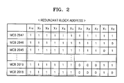
- FIG. 2 illustrates a table for explaining addresses of main cell blocks used as remapping blocks of FIG. 1 ;
- FIG. 3 illustrates a circuit diagram of a remapping block mapping storage circuit of FIG. 1 according to an embodiment
- FIG. 4 illustrates a main/remapping block address MUX unit of FIG. 1 according to an embodiment.
- FIG. 1 illustrates a NAND flash memory device 100 according to an embodiment.
- the NAND flash memory device 100 may include a memory cell array 110 , a row decoder unit 120 , a remapping block mapping controlling unit 130 , and a row pre-decoder 140 .
- a memory cell array 110 may include a plurality of memory blocks. Each of the memory blocks may include a plurality of floating gate type flash memory cells arranged in an array. In FIG. 1 , the flash memory cell includes 2048 main cell blocks MCB 0 through MCB 2047 .
- some main cell blocks (e.g., MCB 2047 through MCB 2018 ), which run from the main cell block MCB 2047 having the uppermost address and a predetermined main cell block counted from the main cell bock MCB 2047 in reverse order by a predetermined number (e.g., 3O), may be used as remapping blocks RCB 0 through RCB 29 for replacing bad blocks in the main cell blocks MCB 0 through MCB 2047 .
- a predetermined number e.g., 3O
- the row decoder unit 120 may include row decoders that are respectively connected to the main cell blocks MCB 0 through MCB 2047 .
- Each row decoder may generate a block selection signal for decoding block address signals Pi, Qi, and Ri, and selecting a corresponding main cell block from among the main cell blocks MCB 0 through MCB 2047 .
- the remapping block mapping controlling unit 130 may compare a bad block address ADDR_BADBLK ⁇ 10:0> to an external block address ADDR_MAIN ⁇ 10:0> output from an external source, may generate a bad block flag signal nBAD_FLAG, may select one of the external block address ADDR_MAIN ⁇ 10:0> and a remapping block address ADDR_REPAIR ⁇ 4:0> in response to the bad block flag signal nBAD_FLAG, and may output a row address signal X_ADDR ⁇ 10:0>.
- the row address signal X_ADDR ⁇ 10:0> may be decoded by the row pre-decoder 140 to generate the block address signals Pi, Qi, and Ri.
- the remapping block mapping controlling unit 130 may include a bad block address storage circuit 132 , a comparing unit 134 , a remapping block mapping storage circuit 136 , and a main/remapping block address MUX unit 138 .
- the bad block address storage circuit 132 may store an address of a bad block from among the main cell blocks MCB 0 through MCB 2017 .
- the bad block address storage circuit 132 may be a register.
- the bad block address storage circuit 132 may generate the remapping addresses RBM 0 through RBM 29 and a remapping enable signal RME, which match the bad block address ADDR_BADBLK ⁇ 10:0>, in order to replace the bad block with the remapping blocks MCB 2047 through MCB 2018 or RCB 0 through RCB 29 .
- the comparing unit 134 may compare the external block address ADDR_MAIN ⁇ 10:0> and the bad block address ADDR_BADBLK ⁇ 10:0> stored in the bad block address storage circuit 132 .
- the comparing unit 134 may generate the bad block flag signal nBAD_FLAG having a logic low level when the external block address ADDR_MAIN ⁇ 10:0>is identical to the bad block address ADDR_BADBLK ⁇ 10:0>, and may generate the bad block flag signal nBAD_FLAG having a logic high level when the external block address ADDR_MAIN ⁇ 10:0> is not identical to the bad block address ADDR_BADBLK ⁇ 10:0>.
- the remapping block mapping storage circuit 136 may provide the remapping block address ADDR_REPAIR ⁇ 4:0> in response to the remapping addresses RBM 0 through RBM 29 .
- the remapping block address ADDR_REPAIR ⁇ 4:0> may select the remapping blocks MCB 2047 -MCB 2018 or RCB 0 -RCB 29 for replacing the bad block.
- FIG. 2 with regard to an address of the remapping blocks MCB 2047 through MCB 2018 , from among 11 bit X[10:0] addresses, the top 6 bit X[10:5] addresses are set as “1”, and the bottom 5 bit X[4:0] address are from 11111 to 00010.
- FIG. 3 illustrates a circuit diagram of the remapping block mapping storage circuit 136 of FIG. 1 according to an embodiment.
- the remapping block mapping storage circuit 136 may include a plurality of cell transistors CT arranged in rows and columns.
- the cell transistors CT may be connected to a power voltage VDD source and ground voltage VSS source.
- the cell transistors CT provide the remapping block address ADDR_REPAIR ⁇ 4:0> corresponding to the remapping addresses RBM 0 through RBM 29 in response to the remapping addresses RBM 0 through RBM 29 .
- the remapping block address ADDR_REPAIR ⁇ 4:0> may be generated as 11111.
- the remapping block address ADDR_REPAIR ⁇ 4:0> set as 11111 is identical to the bottom 5 bit X[4:0] address of the remapping block MCB 2047 of FIG. 2 .
- the remapping block address ADDR_REPAIR ⁇ 4:0> may be generated as 11110.
- the remapping block address ADDR_REPAIR ⁇ 4:0> set as 11110 is identical to the bottom 5 bit X[4:0] address of the remapping block MCB 2046 of FIG. 2 .
- This correspondence may be carried forth throughout the remapping addresses, such that when the remapping address RBM 29 is activated, the remapping block address ADDR_REPAIR ⁇ 4:0> may be generated as 00010.
- the remapping block address ADDR_REPAIR ⁇ 4:0>set as 00010 is identical to the bottom 5 bit X[4:0] of the remapping block MCB 2018 of FIG. 2 .
- FIG. 4 illustrates the main/remapping block address MUX unit 138 of FIG. 1 according to an embodiment.
- the main/remapping block address MUX unit 138 may select one of an external block address ADDR_MAIN ⁇ 4:0> and the remapping block address ADDR_REPAIR ⁇ 4:0> in response to the bad block flag signal nBAD_FLAG, may output a row address signal X_ADDR ⁇ 4:0>, and then may output an external block address ADDR_MAIN ⁇ 10:5> to a row address signal X_ADDR ⁇ 10:5>.
- the main/remapping block address MUX unit 138 may include a first AND gate 401 , to which the bad block flag signal nBAD_FLAG and an external block address bit ADDR_MAIN ⁇ 0> are input, a second AND gate 402 , to which a reverse signal of the bad block flag signal nBAD_FLAG and a remapping block address bit ADDR_REPAIR ⁇ 0> are input, a first NOR gate 403 , to which outputs of the first and second AND gates 401 and 402 are input, and a first inverter 404 , to which an output of the first NOR gate 403 is input, and which outputs a row address signal X_ADDR ⁇ 0>.
- the bad block flag signal nBAD_FLAG has a logic high level, i.e., when the comparing unit 134 determines that the external block address ADDR_MAIN ⁇ 10:0> is not identical to the bad block address ADDR_BADBLK ⁇ 10:0>, the external block address ADDR_MAIN ⁇ 0> may be output as the row address signal X_ADDR ⁇ 0>.
- the remapping block address bit ADDR_REPAIR ⁇ 0> may be output as the row address signal X_ADDR ⁇ 0>.
- main/remapping block address MUX unit 138 selects one of an external block address ADDR_MAIN ⁇ 4:1> and a remapping block address ADDR_REPAIR ⁇ 4:1> in response to the bad block flag signal nBAD_FLAG, and then outputs a row address signal X_ADDR ⁇ 4:1>.
- the main/remapping block address MUX unit 138 may include a third AND gate 421 , to which the bad block flag signal nBAD_FLAG and an external block address bit ADDR_MAIN ⁇ 5> are input, a fourth AND gate 422 , to which a reverse signal of the bad block flag signal nBAD_FLAG and a logic high level of the power voltage VDD are input, a second NOR gate 423 , to which outputs of the third and fourth AND gates 421 and 422 are input, and an inverter 404 , to which an output of the second NOR gate 423 is input, and which outputs a low address signal X_ADDR ⁇ 5>.
- the external block address bit ADDR_MAIN ⁇ 5> is output to the row address signal X_ADDR ⁇ 5>.
- the bad block flag signal nBAD_FLAG has a logic low level
- a logic high level of the power voltage VDD is output to the low address signal X_ADDR ⁇ 5>.
- the main/remapping block address MUX unit 138 selects one of the external block address ADDR_MAIN ⁇ 10:5> and the logic high level of the power voltage VDD in response to the bad block flag signal nBAD_FLAG, and then outputs the row address signal X_ADDR ⁇ 10:5>.
- the bad block flag signal nBAD_FLAG When the bad block flag signal nBAD_FLAG has a logic low level, the bad block needs to be replaced with the remapping blocks MCB 2047 through MCB 2018 .
- the row address signal X_ADDR ⁇ 10:5> is generated as “1”.
- the row address signal X_ADDR ⁇ 10:5> is decoded by the row pre-decoder 140 to generate the block address signals Pi, Qi, and Ri.
- the block address signals Pi, Qi, and Ri provide row decoders that are respectively connected to the main cell blocks MCB 0 through MCB 2047 .
- Each row decoder may generate a block cell selection signal for decoding the block address signals Pi, Qi, and Ri, and selecting a corresponding main cell block from among the main cell blocks.
- flash memory devices include a memory cell array including a plurality of main cell blocks, and the main cell blocks have their own exclusive block addresses.
- Each main cell block is connected to a row decoder decoding block address signals, and is selected in response to a block selection signal generated by the row decoder.
- Main cell blocks which are between a main cell block having the uppermost address and a predetermined main cell block counted from the main cell block in reverse order by a predetermined number, are used as redundant blocks for replacing bad blocks in the main cell blocks.
- flash memory devices need to provide redundant block address signals to a row decoder in addition to block address signals provided to the row decoder in order to select redundant blocks. Redundant block signals correspond to address signals of bad blocks. Thus, due to bussing redundant block address signals to row decoders, the chip size of flash memory devices may be increased.
- a memory device e.g., a NAND flash memory device
Landscapes
- Read Only Memory (AREA)
Abstract
Description
- 1. Field
- Embodiments relate to a semiconductor memory device, and more particularly, to a non-volatile memory device having a bad block remapping function and a bad block remapping method.
- 2. Description of the Related Art
- Flash memory devices are non-volatile memory devices for electrically recording and erasing data. Memory cells of a flash memory device are configured in a plurality of blocks, and each of the blocks includes a plurality of pages. In particular, a block is an elementary unit for erasing data stored in a memory cell.
- Flash memory devices program and erase data by using a tunneling effect, in which a particle penetrates a high energy barrier, and a hot carrier effect, in which a hot carrier having a high kinetic energy penetrates an insulating material. Since flash memory devices program and erase data, data can be programmed in a flash memory cell a limited number of times, and the flash memory cell might fail to write data. In addition, due to a variety of restrictions on manufacturing flash memory devices requiring a high integration density, defective flash memory cells might be manufactured.
- During the manufacture or operation of flash memory devices, a fatal problem can occur in a memory cell. A block having at least one defective memory cell is referred to as a bad block. A flash memory device having an at least predetermined number, e.g., at least five, of bad blocks is determined to be a failure article.
- A flash memory device having a predetermined number or less of bad blocks uses a method of managing a bad block. An example of the method includes a bad block mapping method in which a bad block is replaced with a redundant block. The bad block mapping method includes checking an address of the bad block, impeding writing and reading data in the bad block, replacing the bad block with the redundant block, and writing and reading data in the redundant data.
- Embodiments are directed to a non-volatile memory device having a bad block remapping function and a bad block remapping method, which substantially overcome one or more of the problems due to the limitations and disadvantages of the related art.
- It is a feature of an embodiment to provide a non-volatile memory device that does not require separate bussing of remapping block address signals.
- It is another feature of an embodiment to provide a non-volatile memory device that selects remapping blocks using existing block address signals.
- It is yet another feature of an embodiment to provide a bad block remapping method of the non-volatile memory device.
- At least one of the above and other features and advantages may also be realized by providing a non-volatile memory device including a memory cell array including a plurality of main cell blocks, and using a predetermined number of the main cell blocks as remapping blocks for replacing a bad block in the main cell blocks, a row decoder unit decoding a row address signal to generate block address signals addressing the main cell blocks, and a remapping block mapping controlling unit. The remapping block mapping controlling unit is configured to compare an external block address input by an external source and a bad block address stored in a chip, generate a bad block flag signal, generate a remapping block address for selecting the remapping blocks by matching a remapping address with the bad block address, selecting one of the external block address and the remapping block address in response to the bad block flag signal as a selected address, and outputting the row address signal in accordance with the selected address.
- The predetermined number of remapping blocks may include main cell blocks from a main cell block having an uppermost address to a main cell block counted from the main cell block having the upper most address in reverse order up to the predetermined number.
- The row decoder unit may include a row pre-decoder configured to decode the row address to generate the block address signals, and a row decoder connected to each of the main cell blocks and configured to select a corresponding main cell block from among the main cell blocks in response to the block address signals.
- The remapping block mapping controlling unit may include a bad block address storage circuit configured to store the bad block address and generate the remapping address, a comparing unit configured to compare the external block address to the bad block address and generate the bad block flag signal, a remapping block mapping storage circuit configured to generate the remapping block address corresponding to the remapping address in response to the remapping address, and a main/remapping block address MUX unit configured to select the selected address in response to the bad block flag signal, and output the row address signal in accordance with the selected address.
- The bad block address storage circuit may include a register.
- The remapping block mapping storage circuit may include a plurality of cell transistors arranged in rows and columns, and the cell transistors may be electrically connected to a power voltage source or a ground voltage source, and the remapping address may be supplied to gates of the cell transistors.
- The main/remapping block address MUX unit may include a first AND gate to which the bad block flag signal and the external block address are input, a second AND gate to which a reverse signal of the bad block flag signal and a bit of the remapping block address are input, a NOR gate to which outputs of the first and second AND gates are input, and an inverter to which an output of the NOR gate is input and which outputs the row address signal.
- A memory cell in the main cell blocks may be a floating gate type flash memory cell.
- At least one of the above and other features and advantages may also be realized by providing a bad block remapping method of a non-volatile memory device including a plurality of main cell blocks selected by a row address signal, a predetermined number of the main cell blocks serve as remapping blocks to replace a bad block in the main cell blocks. The method includes storing a bad block address for addressing the bad block, generating a remapping address matching the bad block address, comparing an external block address, which is for addressing the main cell blocks and is input from an external source, to the bad block address and generating a bad block flag signal, generating a remapping block address for selecting the remapping blocks in response to a remapping address matching the bad block address, selecting one of the external block address and the remapping block address in response to the bad block flag signal to generate a selected address, and outputting a row address signal in accordance with the selected address.
- A memory cell in the main cell blocks of the non-volatile memory device may be a floating gate type flash memory cell.
- The predetermined number of remapping blocks may include main cell blocks from a main cell block having an uppermost address to a main cell block counted from the main cell block having the upper most address in reverse order up to the predetermined number.
- When the bad block flag signal indicates that the external block address does not equal the bad block address, the external block address may be output as the row address signal.
- When the bad block flag signal indicates that the external block address equals the bad block address, the remapping block address may be output as the row address signal.
- At least one of the above and other features and advantages may also be realized by providing an article of manufacture having a machine accessible medium including data that, when accessed by a machine, cause the machine to perform a method for remapping a non-volatile memory device including a plurality of main cell blocks selected by a row address signal, a predetermined number of the main cell blocks serve as remapping blocks to replace a bad block in the main cell blocks, the method including storing a bad block address for addressing the bad block, generating a remapping address matching the bad block address, comparing an external block address, which is for addressing the main cell blocks and is input from an external source, to the bad block address and generating a bad block flag signal, generating a remapping block address for selecting the remapping blocks in response to a remapping address matching the bad block address, selecting one of the external block address and the remapping block address in response to the bad block flag signal to generate a selected address, and outputting a row address signal in accordance with the selected address.
- The above and other features and advantages will become more apparent to those of ordinary skill in the art by describing in detail exemplary embodiments with reference to the attached drawings, in which:
-
FIG. 1 illustrates a NAND flash memory device according to an embodiment; -
FIG. 2 illustrates a table for explaining addresses of main cell blocks used as remapping blocks ofFIG. 1 ; -
FIG. 3 illustrates a circuit diagram of a remapping block mapping storage circuit ofFIG. 1 according to an embodiment; and -
FIG. 4 illustrates a main/remapping block address MUX unit ofFIG. 1 according to an embodiment. - Korean Patent Application No. 10-2008-0083027, filed on Aug. 25, 2008, in the Korean Intellectual Property Office, and entitled: “Non-Volatile Memory Device and Bad Block Remapping Method,” is incorporated by reference herein in its entirety.
- Example embodiments will now be described more fully hereinafter with reference to the accompanying drawings; however, they may be embodied in different forms and should not be construed as limited to the embodiments set forth herein. Rather, these embodiments are provided so that this disclosure will be thorough and complete, and will fully convey the scope of the invention to those skilled in the art.
- It will be understood that when an element or layer is referred to as being “on,” “connected to,” or “coupled to” another element or layer, it can be directly on, connected or coupled to the other element or layer or intervening elements or layers may be present. In contrast, when an element is referred to as being “directly on,” “directly connected to” or “directly coupled to” another element or layer, there are no intervening elements or layers present. Like numerals refer to like elements throughout. As used herein, the term “and/or” includes any and all combinations of one or more of the associated listed items.
-
FIG. 1 illustrates a NANDflash memory device 100 according to an embodiment. Referring toFIG. 1 , the NANDflash memory device 100 may include amemory cell array 110, arow decoder unit 120, a remapping blockmapping controlling unit 130, and a row pre-decoder 140. - A
memory cell array 110 may include a plurality of memory blocks. Each of the memory blocks may include a plurality of floating gate type flash memory cells arranged in an array. InFIG. 1 , the flash memory cell includes 2048 main cell blocks MCB0 through MCB2047. From among the main cell blocks MCB0 through MCB2047, some main cell blocks (e.g., MCB2047 through MCB2018), which run from the main cell block MCB2047 having the uppermost address and a predetermined main cell block counted from the maincell bock MCB 2047 in reverse order by a predetermined number (e.g., 3O), may be used as remapping blocks RCB0 through RCB29 for replacing bad blocks in the main cell blocks MCB0 through MCB2047. - The
row decoder unit 120 may include row decoders that are respectively connected to the main cell blocks MCB0 through MCB2047. Each row decoder may generate a block selection signal for decoding block address signals Pi, Qi, and Ri, and selecting a corresponding main cell block from among the main cell blocks MCB0 through MCB2047. - The remapping block
mapping controlling unit 130 may compare a bad block address ADDR_BADBLK<10:0> to an external block address ADDR_MAIN<10:0> output from an external source, may generate a bad block flag signal nBAD_FLAG, may select one of the external block address ADDR_MAIN<10:0> and a remapping block address ADDR_REPAIR<4:0> in response to the bad block flag signal nBAD_FLAG, and may output a row address signal X_ADDR<10:0>. The row address signal X_ADDR<10:0> may be decoded by the row pre-decoder 140 to generate the block address signals Pi, Qi, and Ri. - The remapping block
mapping controlling unit 130 may include a bad blockaddress storage circuit 132, a comparingunit 134, a remapping blockmapping storage circuit 136, and a main/remapping blockaddress MUX unit 138. - The bad block
address storage circuit 132 may store an address of a bad block from among the main cell blocks MCB0 through MCB2017. The bad blockaddress storage circuit 132 may be a register. The bad blockaddress storage circuit 132 may generate the remapping addresses RBM0 through RBM29 and a remapping enable signal RME, which match the bad block address ADDR_BADBLK<10:0>, in order to replace the bad block with the remapping blocks MCB2047 through MCB2018 or RCB0 through RCB29. - The comparing
unit 134 may compare the external block address ADDR_MAIN<10:0> and the bad block address ADDR_BADBLK<10:0> stored in the bad blockaddress storage circuit 132. The comparingunit 134 may generate the bad block flag signal nBAD_FLAG having a logic low level when the external block address ADDR_MAIN<10:0>is identical to the bad block address ADDR_BADBLK<10:0>, and may generate the bad block flag signal nBAD_FLAG having a logic high level when the external block address ADDR_MAIN<10:0> is not identical to the bad block address ADDR_BADBLK<10:0>. - The remapping block
mapping storage circuit 136 may provide the remapping block address ADDR_REPAIR<4:0> in response to the remapping addresses RBM0 through RBM29. The remapping block address ADDR_REPAIR<4:0> may select the remapping blocks MCB2047-MCB2018 or RCB0-RCB29 for replacing the bad block. As shown inFIG. 2 , with regard to an address of the remapping blocks MCB2047 through MCB2018, from among 11 bit X[10:0] addresses, the top 6 bit X[10:5] addresses are set as “1”, and thebottom 5 bit X[4:0] address are from 11111 to 00010. -
FIG. 3 illustrates a circuit diagram of the remapping blockmapping storage circuit 136 ofFIG. 1 according to an embodiment. Referring toFIG. 3 , the remapping blockmapping storage circuit 136 may include a plurality of cell transistors CT arranged in rows and columns. The cell transistors CT may be connected to a power voltage VDD source and ground voltage VSS source. The cell transistors CT provide the remapping block address ADDR_REPAIR<4:0> corresponding to the remapping addresses RBM0 through RBM29 in response to the remapping addresses RBM0 through RBM29. - When the remapping enable signal RME, for example, the remapping address RBM0 is activated, the remapping block address ADDR_REPAIR<4:0> may be generated as 11111. Thus, the remapping block address ADDR_REPAIR<4:0> set as 11111 is identical to the
bottom 5 bit X[4:0] address of the remapping block MCB2047 ofFIG. 2 . When the remapping address RBM1 is activated, the remapping block address ADDR_REPAIR<4:0> may be generated as 11110. Thus, the remapping block address ADDR_REPAIR<4:0> set as 11110 is identical to thebottom 5 bit X[4:0] address of the remapping block MCB2046 ofFIG. 2 . This correspondence may be carried forth throughout the remapping addresses, such that when the remapping address RBM29 is activated, the remapping block address ADDR_REPAIR<4:0> may be generated as 00010. The remapping block address ADDR_REPAIR<4:0>set as 00010 is identical to thebottom 5 bit X[4:0] of the remapping block MCB2018 ofFIG. 2 . -
FIG. 4 illustrates the main/remapping blockaddress MUX unit 138 ofFIG. 1 according to an embodiment. Referring toFIG. 4 , the main/remapping blockaddress MUX unit 138 may select one of an external block address ADDR_MAIN<4:0> and the remapping block address ADDR_REPAIR<4:0> in response to the bad block flag signal nBAD_FLAG, may output a row address signal X_ADDR<4:0>, and then may output an external block address ADDR_MAIN<10:5> to a row address signal X_ADDR<10:5>. - The main/remapping block
address MUX unit 138 may include a first ANDgate 401, to which the bad block flag signal nBAD_FLAG and an external block address bit ADDR_MAIN<0> are input, a second ANDgate 402, to which a reverse signal of the bad block flag signal nBAD_FLAG and a remapping block address bit ADDR_REPAIR<0> are input, a first NORgate 403, to which outputs of the first and second ANDgates first inverter 404, to which an output of the first NORgate 403 is input, and which outputs a row address signal X_ADDR<0>. - When the bad block flag signal nBAD_FLAG has a logic high level, i.e., when the comparing
unit 134 determines that the external block address ADDR_MAIN<10:0> is not identical to the bad block address ADDR_BADBLK<10:0>, the external block address ADDR_MAIN<0> may be output as the row address signal X_ADDR<0>. When the bad block flag signal nBAD_FLAG has a logic low level, i.e., when the comparingunit 134 determines that the external block address ADDR_MAIN<10:0> is identical to the bad block address ADDR_BADBLK<10:0>, the remapping block address bit ADDR_REPAIR<0> may be output as the row address signal X_ADDR<0>. Likewise, the main/remapping blockaddress MUX unit 138 selects one of an external block address ADDR_MAIN<4:1> and a remapping block address ADDR_REPAIR<4:1> in response to the bad block flag signal nBAD_FLAG, and then outputs a row address signal X_ADDR<4:1>. - The main/remapping block
address MUX unit 138 may include a third ANDgate 421, to which the bad block flag signal nBAD_FLAG and an external block address bit ADDR_MAIN<5> are input, a fourth ANDgate 422, to which a reverse signal of the bad block flag signal nBAD_FLAG and a logic high level of the power voltage VDD are input, a second NORgate 423, to which outputs of the third and fourth ANDgates inverter 404, to which an output of the second NORgate 423 is input, and which outputs a low address signal X_ADDR<5>. - When the bad block flag signal nBAD_FLAG has a logic high level, the external block address bit ADDR_MAIN<5> is output to the row address signal X_ADDR<5>. When the bad block flag signal nBAD_FLAG has a logic low level, a logic high level of the power voltage VDD is output to the low address signal X_ADDR<5>. Likewise, the main/remapping block
address MUX unit 138 selects one of the external block address ADDR_MAIN<10:5> and the logic high level of the power voltage VDD in response to the bad block flag signal nBAD_FLAG, and then outputs the row address signal X_ADDR<10:5>. - When the bad block flag signal nBAD_FLAG has a logic low level, the bad block needs to be replaced with the remapping blocks MCB2047 through MCB2018. Thus, as illustrated in
FIG. 2 , since the top 6 bit X[10:5] addresses are set as “1” in the remapping blocks MCB2047 through MCB2018, the row address signal X_ADDR<10:5> is generated as “1”. - Referring back to
FIG. 1 , the row address signal X_ADDR<10:5> is decoded by therow pre-decoder 140 to generate the block address signals Pi, Qi, and Ri. The block address signals Pi, Qi, and Ri provide row decoders that are respectively connected to the main cell blocks MCB0 through MCB2047. Each row decoder may generate a block cell selection signal for decoding the block address signals Pi, Qi, and Ri, and selecting a corresponding main cell block from among the main cell blocks. - Generally, flash memory devices include a memory cell array including a plurality of main cell blocks, and the main cell blocks have their own exclusive block addresses. Each main cell block is connected to a row decoder decoding block address signals, and is selected in response to a block selection signal generated by the row decoder. Main cell blocks, which are between a main cell block having the uppermost address and a predetermined main cell block counted from the main cell block in reverse order by a predetermined number, are used as redundant blocks for replacing bad blocks in the main cell blocks.
- However, flash memory devices need to provide redundant block address signals to a row decoder in addition to block address signals provided to the row decoder in order to select redundant blocks. Redundant block signals correspond to address signals of bad blocks. Thus, due to bussing redundant block address signals to row decoders, the chip size of flash memory devices may be increased.
- In contrast, in accordance with embodiments, a memory device, e.g., a NAND flash memory device, may select remapping blocks for replacing bad blocks according to block address signals provided to the row decoder. Accordingly, since separate bussing of remapping block address signals is not required to select previous remapping blocks, the chip size of the memory device may be reduced.
- Exemplary embodiments have been disclosed herein, and although specific terms are employed, they are used and are to be interpreted in a generic and descriptive sense only and not for purpose of limitation. For example, the bad block remapping of embodiments may be implemented firmware or in software, e.g., by an article of manufacture having a machine-accessible medium including data that, when accessed by a machine, cause the machine to remap bad blocks. Accordingly, it will be understood by those of ordinary skill in the art that various changes in form and details may be made without departing from the spirit and scope of the present invention as set forth in the following claims.
Claims (14)
Applications Claiming Priority (2)
| Application Number | Priority Date | Filing Date | Title |
|---|---|---|---|
| KR10-2008-0083027 | 2008-08-25 | ||
| KR1020080083027A KR101535460B1 (en) | 2008-08-25 | 2008-08-25 | Nonvolatile memory device having bad block remapping function and bad block remapping method thereof |
Publications (2)
| Publication Number | Publication Date |
|---|---|
| US20100046292A1 true US20100046292A1 (en) | 2010-02-25 |
| US8050093B2 US8050093B2 (en) | 2011-11-01 |
Family
ID=41696255
Family Applications (1)
| Application Number | Title | Priority Date | Filing Date |
|---|---|---|---|
| US12/458,999 Active 2030-04-23 US8050093B2 (en) | 2008-08-25 | 2009-07-29 | Non-volatile memory device and bad block remapping method |
Country Status (2)
| Country | Link |
|---|---|
| US (1) | US8050093B2 (en) |
| KR (1) | KR101535460B1 (en) |
Cited By (14)
| Publication number | Priority date | Publication date | Assignee | Title |
|---|---|---|---|---|
| US20120110278A1 (en) * | 2010-10-29 | 2012-05-03 | Microsoft Corporation | Remapping of inoperable memory blocks |
| US8830749B2 (en) | 2011-12-02 | 2014-09-09 | SK Hynix Inc. | Semiconductor memory device and method for controlling the same |
| US20150033064A1 (en) * | 2013-07-24 | 2015-01-29 | Microsoft Corporation | Self-identifying memory errors |
| US20160216969A1 (en) * | 2015-01-28 | 2016-07-28 | Qualcomm Incorporated | System and method for adaptively managing registers in an instruction processor |
| US20160232987A1 (en) * | 2014-04-07 | 2016-08-11 | Micron Technology, Inc. | Soft post package repair of memory devices |
| US9570201B2 (en) | 2015-04-17 | 2017-02-14 | Micron Technology, Inc. | Repair of memory devices using volatile and non-volatile memory |
| US9741403B2 (en) | 2014-11-12 | 2017-08-22 | Micron Technology, Inc. | Apparatuses and methods to perform post package trim |
| US20180268921A1 (en) * | 2017-03-20 | 2018-09-20 | Samsung Electronics Co., Ltd. | Nonvolatile memory device and memory system including the same |
| US10832791B2 (en) | 2019-01-24 | 2020-11-10 | Micron Technology, Inc. | Apparatuses and methods for soft post-package repair |
| CN114911719A (en) * | 2022-05-10 | 2022-08-16 | 南京英锐创电子科技有限公司 | Memory data access method and device and computer equipment |
| US11456028B2 (en) * | 2020-03-06 | 2022-09-27 | Honda Motor Co., Ltd. | Semiconductor device and control method thereof |
| US20230056231A1 (en) * | 2021-08-20 | 2023-02-23 | SK Hynix Inc. | Memory, memory system and operation method of memory system |
| US20240071559A1 (en) * | 2008-04-09 | 2024-02-29 | Rambus Inc. | Controller to detect malfunctioning address of memory device |
| US11984185B2 (en) | 2021-04-07 | 2024-05-14 | Micron Technology, Inc. | Apparatuses and methods for zone-based soft post-package repair |
Families Citing this family (4)
| Publication number | Priority date | Publication date | Assignee | Title |
|---|---|---|---|---|
| KR101086876B1 (en) * | 2009-09-30 | 2011-11-25 | 주식회사 하이닉스반도체 | Semiconductor storage system that manages spare area flexibly and its control method |
| KR101280181B1 (en) * | 2010-05-18 | 2013-07-05 | 삼성전자주식회사 | Memory system and method for managing reserved area of flash translation layer in memory system |
| US9032244B2 (en) | 2012-11-16 | 2015-05-12 | Microsoft Technology Licensing, Llc | Memory segment remapping to address fragmentation |
| KR102070729B1 (en) * | 2013-11-12 | 2020-03-02 | 삼성전자주식회사 | Semiconductor memory device and memory system comprising the same |
Citations (4)
| Publication number | Priority date | Publication date | Assignee | Title |
|---|---|---|---|---|
| US5841957A (en) * | 1996-05-23 | 1998-11-24 | Acti Technology Corp. | Programmable I/O remapper for partially defective memory devices |
| US6625071B2 (en) * | 2001-02-08 | 2003-09-23 | Fujitsu Limited | Memory circuit having block address switching function |
| US6956769B2 (en) * | 2002-03-04 | 2005-10-18 | Samsung Electronics Co., Ltd. | Semiconductor memory device with a flexible redundancy scheme |
| US7434122B2 (en) * | 2004-08-04 | 2008-10-07 | Samsung Electronics Co., Ltd. | Flash memory device for performing bad block management and method of performing bad block management of flash memory device |
Family Cites Families (1)
| Publication number | Priority date | Publication date | Assignee | Title |
|---|---|---|---|---|
| KR100512933B1 (en) * | 2002-01-09 | 2005-09-07 | 삼성전자주식회사 | Semiconductor memory device and block select signal generating method thereof |
-
2008
- 2008-08-25 KR KR1020080083027A patent/KR101535460B1/en active Active
-
2009
- 2009-07-29 US US12/458,999 patent/US8050093B2/en active Active
Patent Citations (4)
| Publication number | Priority date | Publication date | Assignee | Title |
|---|---|---|---|---|
| US5841957A (en) * | 1996-05-23 | 1998-11-24 | Acti Technology Corp. | Programmable I/O remapper for partially defective memory devices |
| US6625071B2 (en) * | 2001-02-08 | 2003-09-23 | Fujitsu Limited | Memory circuit having block address switching function |
| US6956769B2 (en) * | 2002-03-04 | 2005-10-18 | Samsung Electronics Co., Ltd. | Semiconductor memory device with a flexible redundancy scheme |
| US7434122B2 (en) * | 2004-08-04 | 2008-10-07 | Samsung Electronics Co., Ltd. | Flash memory device for performing bad block management and method of performing bad block management of flash memory device |
Cited By (29)
| Publication number | Priority date | Publication date | Assignee | Title |
|---|---|---|---|---|
| US12230350B2 (en) * | 2008-04-09 | 2025-02-18 | Rambus Inc. | Controller to detect malfunctioning address of memory device |
| US20240071559A1 (en) * | 2008-04-09 | 2024-02-29 | Rambus Inc. | Controller to detect malfunctioning address of memory device |
| US9092357B2 (en) * | 2010-10-29 | 2015-07-28 | Microsoft Technology Licensing, Llc | Remapping of inoperable memory blocks |
| US20120110278A1 (en) * | 2010-10-29 | 2012-05-03 | Microsoft Corporation | Remapping of inoperable memory blocks |
| US8830749B2 (en) | 2011-12-02 | 2014-09-09 | SK Hynix Inc. | Semiconductor memory device and method for controlling the same |
| US9875810B2 (en) * | 2013-07-24 | 2018-01-23 | Microsoft Technology Licensing, Llc | Self-identifying memory errors |
| US20150033064A1 (en) * | 2013-07-24 | 2015-01-29 | Microsoft Corporation | Self-identifying memory errors |
| WO2015013153A3 (en) * | 2013-07-24 | 2015-06-25 | Microsoft Corporation | Self-identifying memory errors |
| KR102318237B1 (en) | 2014-04-07 | 2021-10-29 | 마이크론 테크놀로지, 인크. | Soft post package repair of memory devices |
| KR20200128443A (en) * | 2014-04-07 | 2020-11-12 | 마이크론 테크놀로지, 인크. | Soft post package repair of memory devices |
| US9793008B2 (en) | 2014-04-07 | 2017-10-17 | Micron Technology, Inc. | Soft post package repair of memory devices |
| US9922729B2 (en) | 2014-04-07 | 2018-03-20 | Micron Technology, Inc. | Soft post package repair of memory devices |
| KR20190027953A (en) * | 2014-04-07 | 2019-03-15 | 마이크론 테크놀로지, 인크. | Soft post package repair of memory devices |
| US20160232987A1 (en) * | 2014-04-07 | 2016-08-11 | Micron Technology, Inc. | Soft post package repair of memory devices |
| KR102174183B1 (en) * | 2014-04-07 | 2020-11-05 | 마이크론 테크놀로지, 인크. | Soft post package repair of memory devices |
| US9558851B2 (en) * | 2014-04-07 | 2017-01-31 | Micron Technology, Inc. | Soft post package repair of memory devices |
| US9741403B2 (en) | 2014-11-12 | 2017-08-22 | Micron Technology, Inc. | Apparatuses and methods to perform post package trim |
| US20160216969A1 (en) * | 2015-01-28 | 2016-07-28 | Qualcomm Incorporated | System and method for adaptively managing registers in an instruction processor |
| US9570201B2 (en) | 2015-04-17 | 2017-02-14 | Micron Technology, Inc. | Repair of memory devices using volatile and non-volatile memory |
| CN108628757A (en) * | 2017-03-20 | 2018-10-09 | 三星电子株式会社 | Non-volatile memory devices and storage system including it |
| US10622091B2 (en) * | 2017-03-20 | 2020-04-14 | Samsung Electronics Co., Ltd. | Nonvolatile memory device and memory system including the same |
| US20180268921A1 (en) * | 2017-03-20 | 2018-09-20 | Samsung Electronics Co., Ltd. | Nonvolatile memory device and memory system including the same |
| US11145387B2 (en) | 2019-01-24 | 2021-10-12 | Micron Technology, Inc. | Apparatuses and methods for soft post-package repair |
| US10832791B2 (en) | 2019-01-24 | 2020-11-10 | Micron Technology, Inc. | Apparatuses and methods for soft post-package repair |
| US11456028B2 (en) * | 2020-03-06 | 2022-09-27 | Honda Motor Co., Ltd. | Semiconductor device and control method thereof |
| US11984185B2 (en) | 2021-04-07 | 2024-05-14 | Micron Technology, Inc. | Apparatuses and methods for zone-based soft post-package repair |
| US20230056231A1 (en) * | 2021-08-20 | 2023-02-23 | SK Hynix Inc. | Memory, memory system and operation method of memory system |
| US11817169B2 (en) * | 2021-08-20 | 2023-11-14 | SK Hynix Inc. | Memory, memory system and operation method of memory system |
| CN114911719A (en) * | 2022-05-10 | 2022-08-16 | 南京英锐创电子科技有限公司 | Memory data access method and device and computer equipment |
Also Published As
| Publication number | Publication date |
|---|---|
| KR101535460B1 (en) | 2015-07-10 |
| KR20100024258A (en) | 2010-03-05 |
| US8050093B2 (en) | 2011-11-01 |
Similar Documents
| Publication | Publication Date | Title |
|---|---|---|
| US8050093B2 (en) | Non-volatile memory device and bad block remapping method | |
| US8625339B2 (en) | Multi-cell per memory-bit circuit and method | |
| US9748001B2 (en) | Bad column management with bit information in non-volatile memory systems | |
| US6532181B2 (en) | Semiconductor memory device having redundant circuitry for replacing defective memory cell | |
| EP2564388B1 (en) | Non-volatile memory and method with even/odd combined interleaved block decoding with adapted word line activation circuitry | |
| CN1112706C (en) | Semiconductor capable of imaging bad block | |
| US8644072B2 (en) | Three dimensionally stacked memory and the isolation of memory cell layer | |
| US20090180339A1 (en) | Semiconductor memory device with three-dimensional array and repair method thereof | |
| CN112908396B (en) | Memory device with repair matching mechanism and operation method thereof | |
| US8477547B2 (en) | Semiconductor memory device and method of operating the same | |
| US7289364B2 (en) | Programmable memory device with an improved redundancy structure | |
| US20120075943A1 (en) | Method and Apparatus for Memory Repair With Redundant Columns | |
| US7830720B2 (en) | Methods of programming non-volatile semiconductor memory devices using different program verification operations and related devices | |
| US11211142B2 (en) | Memory repair scheme | |
| JP4439539B2 (en) | Nonvolatile semiconductor memory and test method thereof | |
| JP4387547B2 (en) | Nonvolatile semiconductor memory | |
| US7755956B2 (en) | Non-volatile semiconductor memory and method for replacing defective blocks thereof | |
| US7911841B2 (en) | Non-volatile memory device and method for operating the memory device | |
| US8125839B2 (en) | Memory device and method reducing fluctuation of read voltage generated during read while write operation | |
| JP4950816B2 (en) | Semiconductor memory | |
| US11710531B2 (en) | Memory redundancy repair | |
| CN120032695A (en) | Column redundancy circuit and memory device including the same |
Legal Events
| Date | Code | Title | Description |
|---|---|---|---|
| AS | Assignment |
Owner name: SAMSUNG ELECTRONICS CO., LTD.,KOREA, REPUBLIC OF Free format text: ASSIGNMENT OF ASSIGNORS INTEREST;ASSIGNORS:HAHN, WOOK-GHEE;SON, JAI-ICK;LEE, YOUN-YEOL;REEL/FRAME:023077/0435 Effective date: 20090713 Owner name: SAMSUNG ELECTRONICS CO., LTD., KOREA, REPUBLIC OF Free format text: ASSIGNMENT OF ASSIGNORS INTEREST;ASSIGNORS:HAHN, WOOK-GHEE;SON, JAI-ICK;LEE, YOUN-YEOL;REEL/FRAME:023077/0435 Effective date: 20090713 |
|
| STCF | Information on status: patent grant |
Free format text: PATENTED CASE |
|
| FPAY | Fee payment |
Year of fee payment: 4 |
|
| MAFP | Maintenance fee payment |
Free format text: PAYMENT OF MAINTENANCE FEE, 8TH YEAR, LARGE ENTITY (ORIGINAL EVENT CODE: M1552); ENTITY STATUS OF PATENT OWNER: LARGE ENTITY Year of fee payment: 8 |
|
| MAFP | Maintenance fee payment |
Free format text: PAYMENT OF MAINTENANCE FEE, 12TH YEAR, LARGE ENTITY (ORIGINAL EVENT CODE: M1553); ENTITY STATUS OF PATENT OWNER: LARGE ENTITY Year of fee payment: 12 |