US20090051663A1 - Recovering image system - Google Patents
Recovering image system Download PDFInfo
- Publication number
- US20090051663A1 US20090051663A1 US11/894,217 US89421707A US2009051663A1 US 20090051663 A1 US20090051663 A1 US 20090051663A1 US 89421707 A US89421707 A US 89421707A US 2009051663 A1 US2009051663 A1 US 2009051663A1
- Authority
- US
- United States
- Prior art keywords
- reset
- panel
- signals
- data signals
- image system
- Prior art date
- Legal status (The legal status is an assumption and is not a legal conclusion. Google has not performed a legal analysis and makes no representation as to the accuracy of the status listed.)
- Granted
Links
Images


Classifications
-
- G—PHYSICS
- G06—COMPUTING OR CALCULATING; COUNTING
- G06F—ELECTRIC DIGITAL DATA PROCESSING
- G06F3/00—Input arrangements for transferring data to be processed into a form capable of being handled by the computer; Output arrangements for transferring data from processing unit to output unit, e.g. interface arrangements
- G06F3/01—Input arrangements or combined input and output arrangements for interaction between user and computer
- G06F3/03—Arrangements for converting the position or the displacement of a member into a coded form
- G06F3/041—Digitisers, e.g. for touch screens or touch pads, characterised by the transducing means
- G06F3/0412—Digitisers structurally integrated in a display
-
- G—PHYSICS
- G06—COMPUTING OR CALCULATING; COUNTING
- G06F—ELECTRIC DIGITAL DATA PROCESSING
- G06F3/00—Input arrangements for transferring data to be processed into a form capable of being handled by the computer; Output arrangements for transferring data from processing unit to output unit, e.g. interface arrangements
- G06F3/01—Input arrangements or combined input and output arrangements for interaction between user and computer
- G06F3/03—Arrangements for converting the position or the displacement of a member into a coded form
- G06F3/041—Digitisers, e.g. for touch screens or touch pads, characterised by the transducing means
- G06F3/0416—Control or interface arrangements specially adapted for digitisers
- G06F3/0418—Control or interface arrangements specially adapted for digitisers for error correction or compensation, e.g. based on parallax, calibration or alignment
- G06F3/04184—Synchronisation with the driving of the display or the backlighting unit to avoid interferences generated internally
-
- G—PHYSICS
- G09—EDUCATION; CRYPTOGRAPHY; DISPLAY; ADVERTISING; SEALS
- G09G—ARRANGEMENTS OR CIRCUITS FOR CONTROL OF INDICATING DEVICES USING STATIC MEANS TO PRESENT VARIABLE INFORMATION
- G09G3/00—Control arrangements or circuits, of interest only in connection with visual indicators other than cathode-ray tubes
- G09G3/20—Control arrangements or circuits, of interest only in connection with visual indicators other than cathode-ray tubes for presentation of an assembly of a number of characters, e.g. a page, by composing the assembly by combination of individual elements arranged in a matrix no fixed position being assigned to or needed to be assigned to the individual characters or partial characters
- G09G3/34—Control arrangements or circuits, of interest only in connection with visual indicators other than cathode-ray tubes for presentation of an assembly of a number of characters, e.g. a page, by composing the assembly by combination of individual elements arranged in a matrix no fixed position being assigned to or needed to be assigned to the individual characters or partial characters by control of light from an independent source
- G09G3/36—Control arrangements or circuits, of interest only in connection with visual indicators other than cathode-ray tubes for presentation of an assembly of a number of characters, e.g. a page, by composing the assembly by combination of individual elements arranged in a matrix no fixed position being assigned to or needed to be assigned to the individual characters or partial characters by control of light from an independent source using liquid crystals
- G09G3/3611—Control of matrices with row and column drivers
-
- G—PHYSICS
- G09—EDUCATION; CRYPTOGRAPHY; DISPLAY; ADVERTISING; SEALS
- G09G—ARRANGEMENTS OR CIRCUITS FOR CONTROL OF INDICATING DEVICES USING STATIC MEANS TO PRESENT VARIABLE INFORMATION
- G09G2300/00—Aspects of the constitution of display devices
- G09G2300/04—Structural and physical details of display devices
- G09G2300/0439—Pixel structures
- G09G2300/0443—Pixel structures with several sub-pixels for the same colour in a pixel, not specifically used to display gradations
- G09G2300/0447—Pixel structures with several sub-pixels for the same colour in a pixel, not specifically used to display gradations for multi-domain technique to improve the viewing angle in a liquid crystal display, such as multi-vertical alignment [MVA]
-
- G—PHYSICS
- G09—EDUCATION; CRYPTOGRAPHY; DISPLAY; ADVERTISING; SEALS
- G09G—ARRANGEMENTS OR CIRCUITS FOR CONTROL OF INDICATING DEVICES USING STATIC MEANS TO PRESENT VARIABLE INFORMATION
- G09G2310/00—Command of the display device
- G09G2310/06—Details of flat display driving waveforms
- G09G2310/061—Details of flat display driving waveforms for resetting or blanking
Definitions
- the invention relates to a recovering image system, and in particular relates to a recovering image system for a LCD panel with touch panel.
- the MVA (Multi-domain Vertical Alignment) panels have a tendency for showing a domain disturbance for a long period of time after mechanical stress occurs on the touch panel (or MVA panel). Accordingly, it makes the MVA panel less useful for touch panel applications since hand written information leaves undesired traces of push domains by the stylus. As long as the panel is only refreshed, this disturbance will not disappear.
- the recovering image system comprises a data inputting device, a driver and a panel.
- the data inputting device outputs digital data signals.
- the driver device receives the digital data signals, converts the digital data signals into analog data signals, and outputs the analog data signals or resets data signals according to timing control signals.
- the panel receives the analog data signals or the reset data signals and displays normal images, reset images or both according to the analog data signals and the reset data signals.
- the recovering image system comprises a data inputting device, a driver and a panel.
- the driver device comprises a refresh data unit, a AND logic circuit, a timing control unit and a digital to analog converter (DAC).
- the data inputting device outputs digital data signals.
- the refresh data unit receives the digital data signal from the data inputting device and outputs serial digital signals.
- the AND logic circuit receives the serial digital signals and the timing control signals to output logic circuit signals.
- the timing control unit outputs the timing control signals according to a reset enable signal and a reset rate signal.
- the digital to analog converter converts the logic circuit signals into the analog data signals or the reset data signals according to the timing control signals.
- the panel receives the analog data signals or the reset data signals to display normal images, reset images or both according to the analog data signals and the reset data signals.
- the panel displays the reset images.
- the driver device outputs the analog data signals, the panel displays the normal images.
- FIG. 1 is a schematic diagram of an image system without recovering
- FIG. 2 is a schematic diagram of a recovering image system according to an embodiment of the invention.
- FIG. 3 is a schematic diagram of a panel frame reset according to another embodiment of the invention.
- FIG. 4 is a schematic diagram of a panel row reset according to another embodiment of the invention.
- FIG. 5 is a schematic diagram of a panel area reset according to another embodiment of the invention.
- FIG. 6 schematically shows another embodiment of a system for displaying images.
- FIG. 1 is a schematic diagram of an image system 100 without recovering.
- Image system 100 comprises data inputting device 110 , driver IC 150 and panel 180 .
- Panel 180 comprises a LCD panel and a touch panel. The touch panel is disposed on top of the LCD panel.
- Driver IC 150 comprises memory 152 , refresh data unit 154 and digital to analog converter 158 (DAC).
- Data inputting device 110 directly outputs digital data signals to refresh data unit 154 or indirectly outputs digital data signals through memory 152 to refresh data unit 154 .
- Refresh data unit 154 outputs serial digital signals S 154 to digital to analog converter 158 .
- Digital to analog converter 158 converts serial digital signals S 154 into analog data signals S 158 for the panel 180 .
- Panel 180 receives analog data signals S 158 to display normal images.
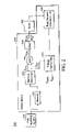
- FIG. 2 is a schematic diagram of recovering image system 200 according to an embodiment of the invention.
- Recovering image system 200 comprises data inputting device 210 , a driver device 250 and panel 280 .
- the drive device 250 can be a drive IC.
- Panel 280 can comprise a LCD panel and a touch panel.
- the touch panel provides signals to represent a push domain area.
- the touch panel is disposed on top of the LCD panel.
- Driver IC 250 comprises memory 252 , refresh data unit 254 , timing control unit 255 , AND logic circuit 256 , digital to analog converter (DAC) 258 and Push Domain Detection unit 259 .
- Data inputting device 210 directly outputs digital data signals to refresh data unit 254 or indirectly outputs digital data signals through memory 252 to refresh data unit 254 .
- Refresh data unit 254 outputs digital signals to AND logic circuit 256 .
- AND logic circuit 256 receives digital signals S 254 and timing control signal S 255 and outputs logic circuit signal S 256 according to digital signals S 254 and timing control signal S 255 .
- Digital to analog converter (DAC) 258 receives logic circuit signal S 256 from AND logic circuit 256 .
- Digital to analog converter 258 converts logic circuit signal S 256 into analog data signals S 258 or reset data signals S 259 for panel 280 .
- Panel 280 receives analog data signals S 258 to display normal images when timing control signal S 255 is disabled. Otherwise, panel 280 receives reset data signals S 259 to display reset images when timing control signal S 255 is enabled.
- one frame can comprise normal images, reset images or both. The detail is discussed in following embodiments of the invention in FIGS. 3 , 4 and 5 .
- Timing control unit 255 outputs timing control signal S 255 according to reset enable signal S enable and reset rate signal S rate .
- Reset signal S enable can control driver IC 250 to reset panel 280 or not.
- Reset rate signal S rate can control the reset rate of panel 280 and is adjustable by another controller (not shown).
- timing control signal S 255 is low voltage level (logic 0)
- logic circuit signal S 256 is low voltage level when digital signals S 254 is high or low voltage level.
- panel 280 is reset. After resetting panel 280 , the panel will show the normal images again.
- Timing control circuit unit 255 can output timing control signal S 255 to reset panel 280 at variable reset rates according to reset rate signal S rate .
- panel 280 turns black. The luminance of panel 280 drops according to the reset rate of reset rate signal S rate . By selecting an optimum reset rate, a balance can be found between the visibility of the push domain and the luminance loss.
- timing control unit 255 can output timing control signal S 255 to reset the push domain area of panel 280 according to the corresponding push domain control signal. Due to mechanical stress occurring on panel 280 , push domain Detection unit 259 can detect the push domain area of panel 280 to generate a corresponding push domain control signal for indicating locations of push domain areas of panel 280 . Timing control unit 255 can output timing control signal S 255 for resetting the push domain area of panel 280 according to the corresponding push domain control signals. Summarily, panel 280 can displays the reset images to restore the push domain areas of the panel. The detail is discussed as following.
- panel 280 can be the combination of the MVA (Multi-domain Vertical Alignment) panel and the touch panel. Since the MVA panel has a tendency for showing a domain disturbance for a long period of time after mechanical stress occurs on the touch panel (or MVA panel). According to the above embodiments, timing control circuit unit 255 can output timing control signal S 255 to reset panel 280 at variable reset rates according to reset rate signal S rate . After resetting panel 280 , the panel will show the normal images again and the disturbance will not appear on panel 280 for a long period of time. It makes MVA useful for touch panel applications.
- MVA Multi-domain Vertical Alignment
- FIG. 3 is a schematic diagram of a panel frame reset according to another embodiment of the invention.
- Panel 280 displays the reset images for n consecutive frames and the normal images for m consecutive frames.
- the reset images as shown in FIG. 3 , are blanked, meaning switching off panel 280 to display black images.
- FIG. 4 is a schematic diagram of a panel row reset according to another embodiment of the invention.
- Panel 280 displays reset images at certain rows of one frame for N consecutive frames according to a timing control signal.
- panel 280 displays the reset images on shifted rows of one frame for next N consecutive frames as shown in FIG. 4 .
- the reset images meaning to switch off pixels at certain rows of panel 280 , will scan all areas of panel 280 .
- panel 280 comprises a plurality of pixels at different rows and different columns to form a matrix (not shown).
- FIG. 5 is a schematic diagram of a panel area reset according to another embodiment of the invention.
- Panel 280 display the reset images at first area of one frame for N consecutive frames.
- panel 280 displays the reset images at second area of one frame for next N consecutive frames.
- the reset images meaning to switch off pixels at certain areas of panel 280 , will scan all areas of panel 280 .
- FIG. 6 schematically shows another embodiment of a system for displaying images which, in this case, is implemented as recovering image system 200 or electronic device 600 .
- recovering image system 200 comprises a driver IC 250 and panel 280 of FIG. 2 .
- Recovering image system 200 can form a portion of a variety of electronic devices (in this case, electronic device 600 ).
- electronic device 600 can comprise recovering image system 200 and power supply 700 .
- power supply 700 is operatively coupled to recovering image system 200 and provides power to recovering image system 200 .
- Electronic device 600 can be a mobile phone, digital camera, PDA (personal data assistant), notebook computer, desktop computer, television, GPS (global positioning system), automotive display, avionics display or portable DVD player, for example.
Landscapes
- Engineering & Computer Science (AREA)
- Theoretical Computer Science (AREA)
- General Engineering & Computer Science (AREA)
- Physics & Mathematics (AREA)
- General Physics & Mathematics (AREA)
- Human Computer Interaction (AREA)
- Crystallography & Structural Chemistry (AREA)
- Computer Hardware Design (AREA)
- Chemical & Material Sciences (AREA)
- Control Of Indicators Other Than Cathode Ray Tubes (AREA)
- Controls And Circuits For Display Device (AREA)
- Liquid Crystal (AREA)
- Liquid Crystal Display Device Control (AREA)
Abstract
Description
- 1. Field of the Invention
- The invention relates to a recovering image system, and in particular relates to a recovering image system for a LCD panel with touch panel.
- 2. Description of the Related Art
- The MVA (Multi-domain Vertical Alignment) panels have a tendency for showing a domain disturbance for a long period of time after mechanical stress occurs on the touch panel (or MVA panel). Accordingly, it makes the MVA panel less useful for touch panel applications since hand written information leaves undesired traces of push domains by the stylus. As long as the panel is only refreshed, this disturbance will not disappear.
- A detailed description is given in the following embodiments with reference to the accompanying drawings.
- An embodiment of a recovering image system is provided. The recovering image system comprises a data inputting device, a driver and a panel. The data inputting device outputs digital data signals. The driver device receives the digital data signals, converts the digital data signals into analog data signals, and outputs the analog data signals or resets data signals according to timing control signals. The panel receives the analog data signals or the reset data signals and displays normal images, reset images or both according to the analog data signals and the reset data signals.
- Another embodiment of a recovering image system is provided. The recovering image system comprises a data inputting device, a driver and a panel. The driver device comprises a refresh data unit, a AND logic circuit, a timing control unit and a digital to analog converter (DAC). The data inputting device outputs digital data signals. The refresh data unit receives the digital data signal from the data inputting device and outputs serial digital signals. The AND logic circuit receives the serial digital signals and the timing control signals to output logic circuit signals. The timing control unit outputs the timing control signals according to a reset enable signal and a reset rate signal. The digital to analog converter converts the logic circuit signals into the analog data signals or the reset data signals according to the timing control signals. The panel receives the analog data signals or the reset data signals to display normal images, reset images or both according to the analog data signals and the reset data signals. When the driver device outputs the reset data signals, the panel displays the reset images. When the driver device outputs the analog data signals, the panel displays the normal images.
- The invention can be more fully understood by reading the subsequent detailed description and examples with references made to the accompanying drawings, wherein:
-
FIG. 1 is a schematic diagram of an image system without recovering; and -
FIG. 2 is a schematic diagram of a recovering image system according to an embodiment of the invention; -
FIG. 3 is a schematic diagram of a panel frame reset according to another embodiment of the invention; -
FIG. 4 is a schematic diagram of a panel row reset according to another embodiment of the invention; -
FIG. 5 is a schematic diagram of a panel area reset according to another embodiment of the invention; and -
FIG. 6 schematically shows another embodiment of a system for displaying images. - The following description is of the best-contemplated mode of carrying out the invention. This description is made for the purpose of illustrating the general principles of the invention and should not be taken in a limiting sense. The scope of the invention is best determined by reference to the appended claims.
-
FIG. 1 is a schematic diagram of animage system 100 without recovering.Image system 100 comprisesdata inputting device 110, driver IC 150 andpanel 180.Panel 180 comprises a LCD panel and a touch panel. The touch panel is disposed on top of the LCD panel. Driver IC 150 comprisesmemory 152,refresh data unit 154 and digital to analog converter 158 (DAC).Data inputting device 110 directly outputs digital data signals to refreshdata unit 154 or indirectly outputs digital data signals throughmemory 152 to refreshdata unit 154. Refreshdata unit 154 outputs serial digital signals S154 to digital toanalog converter 158. Digital toanalog converter 158 converts serial digital signals S154 into analog data signals S158 for thepanel 180.Panel 180 receives analog data signals S158 to display normal images. -
FIG. 2 is a schematic diagram of recoveringimage system 200 according to an embodiment of the invention.Recovering image system 200 comprisesdata inputting device 210, adriver device 250 andpanel 280. Thedrive device 250 can be a drive IC.Panel 280 can comprise a LCD panel and a touch panel. The touch panel provides signals to represent a push domain area. The touch panel is disposed on top of the LCD panel. Driver IC 250 comprisesmemory 252,refresh data unit 254,timing control unit 255, ANDlogic circuit 256, digital to analog converter (DAC) 258 and PushDomain Detection unit 259.Data inputting device 210 directly outputs digital data signals to refreshdata unit 254 or indirectly outputs digital data signals throughmemory 252 to refreshdata unit 254. Refreshdata unit 254 outputs digital signals to ANDlogic circuit 256. ANDlogic circuit 256 receives digital signals S254 and timing control signal S255 and outputs logic circuit signal S256 according to digital signals S254 and timing control signal S255. Digital to analog converter (DAC) 258 receives logic circuit signal S256 fromAND logic circuit 256. Digital toanalog converter 258 converts logic circuit signal S256 into analog data signals S258 or reset data signals S259 forpanel 280.Panel 280 receives analog data signals S258 to display normal images when timing control signal S255 is disabled. Otherwise,panel 280 receives reset data signals S259 to display reset images when timing control signal S255 is enabled. In addition, one frame can comprise normal images, reset images or both. The detail is discussed in following embodiments of the invention inFIGS. 3 , 4 and 5. -
Timing control unit 255 outputs timing control signal S255 according to reset enable signal Senable and reset rate signal Srate. Reset signal Senable can control driver IC 250 to resetpanel 280 or not. Reset rate signal Srate can control the reset rate ofpanel 280 and is adjustable by another controller (not shown). - According to an embodiment of the invention, if timing control signal S255 is low voltage level (logic 0), logic circuit signal S256 is low voltage level when digital signals S254 is high or low voltage level. When logic circuit signal S256 is low voltage level,
panel 280 is reset. After resettingpanel 280, the panel will show the normal images again. Timingcontrol circuit unit 255 can output timing control signal S255 to resetpanel 280 at variable reset rates according to reset rate signal Srate. During resettingpanel 280,panel 280 turns black. The luminance ofpanel 280 drops according to the reset rate of reset rate signal Srate. By selecting an optimum reset rate, a balance can be found between the visibility of the push domain and the luminance loss. - According to another embodiment of the invention,
timing control unit 255 can output timing control signal S255 to reset the push domain area ofpanel 280 according to the corresponding push domain control signal. Due to mechanical stress occurring onpanel 280, pushdomain Detection unit 259 can detect the push domain area ofpanel 280 to generate a corresponding push domain control signal for indicating locations of push domain areas ofpanel 280.Timing control unit 255 can output timing control signal S255 for resetting the push domain area ofpanel 280 according to the corresponding push domain control signals. Summarily,panel 280 can displays the reset images to restore the push domain areas of the panel. The detail is discussed as following. - For example,
panel 280 can be the combination of the MVA (Multi-domain Vertical Alignment) panel and the touch panel. Since the MVA panel has a tendency for showing a domain disturbance for a long period of time after mechanical stress occurs on the touch panel (or MVA panel). According to the above embodiments, timingcontrol circuit unit 255 can output timing control signal S255 to resetpanel 280 at variable reset rates according to reset rate signal Srate. After resettingpanel 280, the panel will show the normal images again and the disturbance will not appear onpanel 280 for a long period of time. It makes MVA useful for touch panel applications. -
FIG. 3 is a schematic diagram of a panel frame reset according to another embodiment of the invention.Panel 280 displays the reset images for n consecutive frames and the normal images for m consecutive frames. The reset images, as shown inFIG. 3 , are blanked, meaning switching offpanel 280 to display black images. -
FIG. 4 is a schematic diagram of a panel row reset according to another embodiment of the invention.Panel 280 displays reset images at certain rows of one frame for N consecutive frames according to a timing control signal. Next,panel 280 displays the reset images on shifted rows of one frame for next N consecutive frames as shown inFIG. 4 . The reset images, meaning to switch off pixels at certain rows ofpanel 280, will scan all areas ofpanel 280. In addition,panel 280 comprises a plurality of pixels at different rows and different columns to form a matrix (not shown). -
FIG. 5 is a schematic diagram of a panel area reset according to another embodiment of the invention.Panel 280 display the reset images at first area of one frame for N consecutive frames. Next,panel 280 displays the reset images at second area of one frame for next N consecutive frames. The reset images, meaning to switch off pixels at certain areas ofpanel 280, will scan all areas ofpanel 280. -
FIG. 6 schematically shows another embodiment of a system for displaying images which, in this case, is implemented as recoveringimage system 200 orelectronic device 600. As shown inFIG. 6 , recoveringimage system 200 comprises adriver IC 250 andpanel 280 ofFIG. 2 . Recoveringimage system 200 can form a portion of a variety of electronic devices (in this case, electronic device 600). Generally,electronic device 600 can comprise recoveringimage system 200 andpower supply 700. Further,power supply 700 is operatively coupled to recoveringimage system 200 and provides power to recoveringimage system 200.Electronic device 600 can be a mobile phone, digital camera, PDA (personal data assistant), notebook computer, desktop computer, television, GPS (global positioning system), automotive display, avionics display or portable DVD player, for example. - While the invention has been described by way of example and in terms of preferred embodiment, it is to be understood that the invention is not limited to thereto. To the contrary, it is intended to cover various modifications and similar arrangements (as would be apparent to those skilled in the art). Therefore, the scope of the appended claims should be accorded the broadest interpretation so as to encompass all such modifications and similar arrangements.
Claims (20)
Priority Applications (3)
| Application Number | Priority Date | Filing Date | Title |
|---|---|---|---|
| US11/894,217 US8154522B2 (en) | 2007-08-20 | 2007-08-20 | Recovering image system |
| TW097127600A TWI393109B (en) | 2007-08-20 | 2008-07-21 | Recovering image system |
| CN2008101353787A CN101373288B (en) | 2007-08-20 | 2008-07-30 | restore image system |
Applications Claiming Priority (1)
| Application Number | Priority Date | Filing Date | Title |
|---|---|---|---|
| US11/894,217 US8154522B2 (en) | 2007-08-20 | 2007-08-20 | Recovering image system |
Publications (2)
| Publication Number | Publication Date |
|---|---|
| US20090051663A1 true US20090051663A1 (en) | 2009-02-26 |
| US8154522B2 US8154522B2 (en) | 2012-04-10 |
Family
ID=40381700
Family Applications (1)
| Application Number | Title | Priority Date | Filing Date |
|---|---|---|---|
| US11/894,217 Active 2030-07-06 US8154522B2 (en) | 2007-08-20 | 2007-08-20 | Recovering image system |
Country Status (3)
| Country | Link |
|---|---|
| US (1) | US8154522B2 (en) |
| CN (1) | CN101373288B (en) |
| TW (1) | TWI393109B (en) |
Cited By (1)
| Publication number | Priority date | Publication date | Assignee | Title |
|---|---|---|---|---|
| US11282908B2 (en) | 2017-07-13 | 2022-03-22 | Kunshan Go-Visionox Opto-Electronics Co., Ltd. | Control methods and control devices for display power supply |
Citations (5)
| Publication number | Priority date | Publication date | Assignee | Title |
|---|---|---|---|---|
| US20050140634A1 (en) * | 2003-12-26 | 2005-06-30 | Nec Corporation | Liquid crystal display device, and method and circuit for driving liquid crystal display device |
| US6922183B2 (en) * | 2002-11-01 | 2005-07-26 | Chin-Lung Ting | Multi-domain vertical alignment liquid crystal display and driving method thereof |
| US20050168434A1 (en) * | 2004-01-30 | 2005-08-04 | Chi Mei Optoelectronics Corp. | Driving method of a multi-domain vertical alignment liquid crystal display |
| US20070001980A1 (en) * | 2005-06-30 | 2007-01-04 | Samsung Electronics Co., Ltd. | Timing controllers for display devices, display devices and methods of controlling the same |
| US20070013640A1 (en) * | 2005-07-12 | 2007-01-18 | Che-Li Lin | Source driver and the data switching circuit thereof |
Family Cites Families (3)
| Publication number | Priority date | Publication date | Assignee | Title |
|---|---|---|---|---|
| TW518552B (en) * | 2000-08-18 | 2003-01-21 | Semiconductor Energy Lab | Liquid crystal display device, method of driving the same, and method of driving a portable information device having the liquid crystal display device |
| DE10228523B4 (en) * | 2001-11-14 | 2017-09-21 | Lg Display Co., Ltd. | touch tablet |
| KR101222949B1 (en) * | 2005-09-06 | 2013-01-17 | 엘지디스플레이 주식회사 | A driving circuit of liquid crystal display device and a method for driving the same |
-
2007
- 2007-08-20 US US11/894,217 patent/US8154522B2/en active Active
-
2008
- 2008-07-21 TW TW097127600A patent/TWI393109B/en not_active IP Right Cessation
- 2008-07-30 CN CN2008101353787A patent/CN101373288B/en active Active
Patent Citations (5)
| Publication number | Priority date | Publication date | Assignee | Title |
|---|---|---|---|---|
| US6922183B2 (en) * | 2002-11-01 | 2005-07-26 | Chin-Lung Ting | Multi-domain vertical alignment liquid crystal display and driving method thereof |
| US20050140634A1 (en) * | 2003-12-26 | 2005-06-30 | Nec Corporation | Liquid crystal display device, and method and circuit for driving liquid crystal display device |
| US20050168434A1 (en) * | 2004-01-30 | 2005-08-04 | Chi Mei Optoelectronics Corp. | Driving method of a multi-domain vertical alignment liquid crystal display |
| US20070001980A1 (en) * | 2005-06-30 | 2007-01-04 | Samsung Electronics Co., Ltd. | Timing controllers for display devices, display devices and methods of controlling the same |
| US20070013640A1 (en) * | 2005-07-12 | 2007-01-18 | Che-Li Lin | Source driver and the data switching circuit thereof |
Cited By (1)
| Publication number | Priority date | Publication date | Assignee | Title |
|---|---|---|---|---|
| US11282908B2 (en) | 2017-07-13 | 2022-03-22 | Kunshan Go-Visionox Opto-Electronics Co., Ltd. | Control methods and control devices for display power supply |
Also Published As
| Publication number | Publication date |
|---|---|
| TW200910314A (en) | 2009-03-01 |
| CN101373288A (en) | 2009-02-25 |
| TWI393109B (en) | 2013-04-11 |
| US8154522B2 (en) | 2012-04-10 |
| CN101373288B (en) | 2012-09-05 |
Similar Documents
| Publication | Publication Date | Title |
|---|---|---|
| KR102651651B1 (en) | Display Device and Driving Method Thereof | |
| US10896645B2 (en) | Foldable display device | |
| US20060201931A1 (en) | Touch sensible display device, and driving apparatus and method thereof | |
| US8803780B2 (en) | Liquid crystal display having a function of selecting dot inversion and method of selecting dot inversion thereof | |
| US20080303770A1 (en) | Liquid Crystal Display Device | |
| US9349334B2 (en) | Polarity inversion signal converting method, apparatus and display | |
| US20150325200A1 (en) | Source driver and display device including the same | |
| KR20170111788A (en) | Display driving circuit and display device comprising thereof | |
| US20140015819A1 (en) | Method for Driving Display Device and Display Device | |
| US20080165099A1 (en) | Lcds and methods for driving same | |
| JP2006047847A (en) | Gate line driving circuit | |
| KR20150031967A (en) | Display apparatus and drving method thereof | |
| CN101236722A (en) | Display device and driving method thereof | |
| US7639245B2 (en) | Electro-optical device having both partial and entire screen display modes, and method of driving the same | |
| US10482834B2 (en) | Pixel circuit, display device, display apparatus and driving method | |
| KR101957970B1 (en) | Display device and control method thoreof | |
| US8154522B2 (en) | Recovering image system | |
| US8624815B2 (en) | Liquid crystal display device | |
| US20120026137A1 (en) | Driving apparatus and driving method of display device | |
| KR20190041055A (en) | Display device and driving method thereof | |
| US20080055342A1 (en) | Method for displaying a low-resolution image on a high-resolution display device | |
| US8564521B2 (en) | Data processing device, method of driving the same and display device having the same | |
| US7091942B2 (en) | Electrooptic device and driving method thereof | |
| KR20160113855A (en) | Display apparatus and driving board | |
| US20080012817A1 (en) | Driving method capable of generating AC-converting signals for a display panel by setting pin levels of driving circuits and related apparatus |
Legal Events
| Date | Code | Title | Description |
|---|---|---|---|
| AS | Assignment |
Owner name: TPO DISPLAYS CORP., TAIWAN Free format text: ASSIGNMENT OF ASSIGNORS INTEREST;ASSIGNOR:LINSSEN, RONALD MARIE WILLEM;REEL/FRAME:019782/0321 Effective date: 20070612 |
|
| AS | Assignment |
Owner name: CHIMEI INNOLUX CORPORATION, TAIWAN Free format text: MERGER;ASSIGNOR:TPO DISPLAYS CORP.;REEL/FRAME:025584/0198 Effective date: 20100318 |
|
| STCF | Information on status: patent grant |
Free format text: PATENTED CASE |
|
| AS | Assignment |
Owner name: INNOLUX CORPORATION, TAIWAN Free format text: CHANGE OF NAME;ASSIGNOR:CHIMEI INNOLUX CORPORATION;REEL/FRAME:032621/0718 Effective date: 20121219 |
|
| FPAY | Fee payment |
Year of fee payment: 4 |
|
| MAFP | Maintenance fee payment |
Free format text: PAYMENT OF MAINTENANCE FEE, 8TH YEAR, LARGE ENTITY (ORIGINAL EVENT CODE: M1552); ENTITY STATUS OF PATENT OWNER: LARGE ENTITY Year of fee payment: 8 |
|
| MAFP | Maintenance fee payment |
Free format text: PAYMENT OF MAINTENANCE FEE, 12TH YEAR, LARGE ENTITY (ORIGINAL EVENT CODE: M1553); ENTITY STATUS OF PATENT OWNER: LARGE ENTITY Year of fee payment: 12 |