US20080122064A1 - Semiconductor device - Google Patents
Semiconductor device Download PDFInfo
- Publication number
- US20080122064A1 US20080122064A1 US11/943,142 US94314207A US2008122064A1 US 20080122064 A1 US20080122064 A1 US 20080122064A1 US 94314207 A US94314207 A US 94314207A US 2008122064 A1 US2008122064 A1 US 2008122064A1
- Authority
- US
- United States
- Prior art keywords
- memory chip
- pads
- memory
- power supply
- chip
- Prior art date
- Legal status (The legal status is an assumption and is not a legal conclusion. Google has not performed a legal analysis and makes no representation as to the accuracy of the status listed.)
- Granted
Links
Images


Classifications
-
- H—ELECTRICITY
- H10—SEMICONDUCTOR DEVICES; ELECTRIC SOLID-STATE DEVICES NOT OTHERWISE PROVIDED FOR
- H10W—GENERIC PACKAGES, INTERCONNECTIONS, CONNECTORS OR OTHER CONSTRUCTIONAL DETAILS OF DEVICES COVERED BY CLASS H10
- H10W72/00—Interconnections or connectors in packages
-
- H—ELECTRICITY
- H10—SEMICONDUCTOR DEVICES; ELECTRIC SOLID-STATE DEVICES NOT OTHERWISE PROVIDED FOR
- H10W—GENERIC PACKAGES, INTERCONNECTIONS, CONNECTORS OR OTHER CONSTRUCTIONAL DETAILS OF DEVICES COVERED BY CLASS H10
- H10W72/00—Interconnections or connectors in packages
- H10W72/90—Bond pads, in general
-
- H—ELECTRICITY
- H10—SEMICONDUCTOR DEVICES; ELECTRIC SOLID-STATE DEVICES NOT OTHERWISE PROVIDED FOR
- H10W—GENERIC PACKAGES, INTERCONNECTIONS, CONNECTORS OR OTHER CONSTRUCTIONAL DETAILS OF DEVICES COVERED BY CLASS H10
- H10W90/00—Package configurations
-
- H—ELECTRICITY
- H10—SEMICONDUCTOR DEVICES; ELECTRIC SOLID-STATE DEVICES NOT OTHERWISE PROVIDED FOR
- H10W—GENERIC PACKAGES, INTERCONNECTIONS, CONNECTORS OR OTHER CONSTRUCTIONAL DETAILS OF DEVICES COVERED BY CLASS H10
- H10W72/00—Interconnections or connectors in packages
- H10W72/01—Manufacture or treatment
-
- H—ELECTRICITY
- H10—SEMICONDUCTOR DEVICES; ELECTRIC SOLID-STATE DEVICES NOT OTHERWISE PROVIDED FOR
- H10W—GENERIC PACKAGES, INTERCONNECTIONS, CONNECTORS OR OTHER CONSTRUCTIONAL DETAILS OF DEVICES COVERED BY CLASS H10
- H10W72/00—Interconnections or connectors in packages
- H10W72/071—Connecting or disconnecting
- H10W72/075—Connecting or disconnecting of bond wires
-
- H—ELECTRICITY
- H10—SEMICONDUCTOR DEVICES; ELECTRIC SOLID-STATE DEVICES NOT OTHERWISE PROVIDED FOR
- H10W—GENERIC PACKAGES, INTERCONNECTIONS, CONNECTORS OR OTHER CONSTRUCTIONAL DETAILS OF DEVICES COVERED BY CLASS H10
- H10W72/00—Interconnections or connectors in packages
- H10W72/20—Bump connectors, e.g. solder bumps or copper pillars; Dummy bumps; Thermal bumps
- H10W72/29—Bond pads specially adapted therefor
-
- H—ELECTRICITY
- H10—SEMICONDUCTOR DEVICES; ELECTRIC SOLID-STATE DEVICES NOT OTHERWISE PROVIDED FOR
- H10W—GENERIC PACKAGES, INTERCONNECTIONS, CONNECTORS OR OTHER CONSTRUCTIONAL DETAILS OF DEVICES COVERED BY CLASS H10
- H10W72/00—Interconnections or connectors in packages
- H10W72/50—Bond wires
- H10W72/541—Dispositions of bond wires
- H10W72/547—Dispositions of multiple bond wires
- H10W72/5473—Dispositions of multiple bond wires multiple bond wires connected to a common bond pad
-
- H—ELECTRICITY
- H10—SEMICONDUCTOR DEVICES; ELECTRIC SOLID-STATE DEVICES NOT OTHERWISE PROVIDED FOR
- H10W—GENERIC PACKAGES, INTERCONNECTIONS, CONNECTORS OR OTHER CONSTRUCTIONAL DETAILS OF DEVICES COVERED BY CLASS H10
- H10W72/00—Interconnections or connectors in packages
- H10W72/50—Bond wires
- H10W72/551—Materials of bond wires
- H10W72/552—Materials of bond wires comprising metals or metalloids, e.g. silver
- H10W72/5522—Materials of bond wires comprising metals or metalloids, e.g. silver comprising gold [Au]
-
- H—ELECTRICITY
- H10—SEMICONDUCTOR DEVICES; ELECTRIC SOLID-STATE DEVICES NOT OTHERWISE PROVIDED FOR
- H10W—GENERIC PACKAGES, INTERCONNECTIONS, CONNECTORS OR OTHER CONSTRUCTIONAL DETAILS OF DEVICES COVERED BY CLASS H10
- H10W72/00—Interconnections or connectors in packages
- H10W72/50—Bond wires
- H10W72/59—Bond pads specially adapted therefor
-
- H—ELECTRICITY
- H10—SEMICONDUCTOR DEVICES; ELECTRIC SOLID-STATE DEVICES NOT OTHERWISE PROVIDED FOR
- H10W—GENERIC PACKAGES, INTERCONNECTIONS, CONNECTORS OR OTHER CONSTRUCTIONAL DETAILS OF DEVICES COVERED BY CLASS H10
- H10W72/00—Interconnections or connectors in packages
- H10W72/90—Bond pads, in general
- H10W72/931—Shapes of bond pads
- H10W72/932—Plan-view shape, i.e. in top view
-
- H—ELECTRICITY
- H10—SEMICONDUCTOR DEVICES; ELECTRIC SOLID-STATE DEVICES NOT OTHERWISE PROVIDED FOR
- H10W—GENERIC PACKAGES, INTERCONNECTIONS, CONNECTORS OR OTHER CONSTRUCTIONAL DETAILS OF DEVICES COVERED BY CLASS H10
- H10W72/00—Interconnections or connectors in packages
- H10W72/90—Bond pads, in general
- H10W72/951—Materials of bond pads
-
- H—ELECTRICITY
- H10—SEMICONDUCTOR DEVICES; ELECTRIC SOLID-STATE DEVICES NOT OTHERWISE PROVIDED FOR
- H10W—GENERIC PACKAGES, INTERCONNECTIONS, CONNECTORS OR OTHER CONSTRUCTIONAL DETAILS OF DEVICES COVERED BY CLASS H10
- H10W90/00—Package configurations
- H10W90/20—Configurations of stacked chips
-
- H—ELECTRICITY
- H10—SEMICONDUCTOR DEVICES; ELECTRIC SOLID-STATE DEVICES NOT OTHERWISE PROVIDED FOR
- H10W—GENERIC PACKAGES, INTERCONNECTIONS, CONNECTORS OR OTHER CONSTRUCTIONAL DETAILS OF DEVICES COVERED BY CLASS H10
- H10W90/00—Package configurations
- H10W90/20—Configurations of stacked chips
- H10W90/231—Configurations of stacked chips the stacked chips being on both top and bottom sides of an auxiliary carrier having no electrical connection structure
-
- H—ELECTRICITY
- H10—SEMICONDUCTOR DEVICES; ELECTRIC SOLID-STATE DEVICES NOT OTHERWISE PROVIDED FOR
- H10W—GENERIC PACKAGES, INTERCONNECTIONS, CONNECTORS OR OTHER CONSTRUCTIONAL DETAILS OF DEVICES COVERED BY CLASS H10
- H10W90/00—Package configurations
- H10W90/20—Configurations of stacked chips
- H10W90/24—Configurations of stacked chips at least one of the stacked chips being laterally offset from a neighbouring stacked chip, e.g. chip stacks having a staircase shape
-
- H—ELECTRICITY
- H10—SEMICONDUCTOR DEVICES; ELECTRIC SOLID-STATE DEVICES NOT OTHERWISE PROVIDED FOR
- H10W—GENERIC PACKAGES, INTERCONNECTIONS, CONNECTORS OR OTHER CONSTRUCTIONAL DETAILS OF DEVICES COVERED BY CLASS H10
- H10W90/00—Package configurations
- H10W90/701—Package configurations characterised by the relative positions of pads or connectors relative to package parts
- H10W90/751—Package configurations characterised by the relative positions of pads or connectors relative to package parts of bond wires
- H10W90/752—Package configurations characterised by the relative positions of pads or connectors relative to package parts of bond wires between stacked chips
-
- H—ELECTRICITY
- H10—SEMICONDUCTOR DEVICES; ELECTRIC SOLID-STATE DEVICES NOT OTHERWISE PROVIDED FOR
- H10W—GENERIC PACKAGES, INTERCONNECTIONS, CONNECTORS OR OTHER CONSTRUCTIONAL DETAILS OF DEVICES COVERED BY CLASS H10
- H10W90/00—Package configurations
- H10W90/701—Package configurations characterised by the relative positions of pads or connectors relative to package parts
- H10W90/751—Package configurations characterised by the relative positions of pads or connectors relative to package parts of bond wires
- H10W90/754—Package configurations characterised by the relative positions of pads or connectors relative to package parts of bond wires between a chip and a stacked insulating package substrate, interposer or RDL
Definitions
- the present invention relates to a semiconductor device, and more particularly to a multichip package.
- MCP multichip package
- a memory chip e.g., a random access memory (RAM) or a flash memory and a controller chip thereof are packaged based on the MCP technology
- the plurality of memory chips are laminated in many cases.
- electroconductive pads are respectively provided on a package substrate, a memory chip, and a controller chip, these members are electrically connected with each other by connecting their pads through bonding wires.
- each chip is laminated while assuring a space where wire bonding can be effected near the pad provided on each chip.
- the memory chips to be laminated since the memory chips to be laminated usually have substantially the same size, when these memory chips are simply laminated, the pad on a chip that is arranged on a lower layer side is not exposed, and wire bonding cannot be performed.
- the plurality of memory chips are laminated while being staggered in the same direction so that a pad region of each chip is exposed, a package size becomes large in a staggering direction.
- An aspect of a semiconductor device comprising: a package substrate which has a plurality of pads to which a power supply voltage is supplied on an upper surface thereof; a first memory chip which is arranged on the package substrate and has a first power supply pad provided on a first side and a second power supply pad provided on a second side perpendicular to the first side; and a second memory chip which is translated in a direction along which the first and second power supply pads of the first memory chip are exposed, and arranged on the first memory chip, wherein the first and second power supply pads are provided at diagonal corners of the first memory chip, respectively.
- An aspect of a semiconductor device comprising: a package substrate which has a plurality of pads to which a power supply voltage is supplied on an upper surface thereof; a first memory chip which is arranged on the package substrate and has a first power supply pad provided on a first side and a second power supply pad provided on a second side perpendicular to the first side; a second memory chip which is translated in a direction along which the first and second power supply pads of the first memory chip are exposed, and arranged on the first memory chip; and a third memory chip which is translated in a direction opposite to the translating direction of the second memory chip, and arranged on the second memory chip through a spacer at a position where it overlaps the first memory chip, wherein the first and second power supply pads are provided at diagonal corners of the first memory chip, respectively.
- An aspect of a semiconductor device comprising: a package substrate; a first memory chip which is arranged on the package substrate and has a first power supply pad provided on a first side and a second power supply pad provided on a second side perpendicular to the first side; a second memory chip which is opposite to the first memory chip in a lateral direction, translated in a direction along which the first and second power supply pads of the first memory chip are exposed, and arranged on the first memory chip; and a third memory chip which is translated in a direction opposite to the translating direction of the second memory chip and arranged on the second memory chip, wherein the first and second power supply pads are provided at diagonal corners of the first memory chip, respectively.
- FIG. 1 is a plan view of a multichip package showing a basic configuration of a first embodiment
- FIG. 2 is a cross-sectional view taken along a line II-II in FIG. 1 ;
- FIG. 3 is a plan view of a multichip package showing an application example of the first embodiment
- FIG. 4 is a cross-sectional view taken along a line IV-IV in FIG. 3 ;
- FIG. 5 is a plan view of a multichip package showing a configuration of a second embodiment
- FIG. 6 is a cross-sectional view taken along a line VI-VI in FIG. 5 ;
- FIG. 7 is a plan view of a multichip package showing a basic configuration of a third embodiment
- FIG. 8 is a cross-sectional view taken along a line VIII-VIII in FIG. 7 ;
- FIG. 9 is a plan view showing a configuration depicted in FIG. 7 in stages
- FIG. 10 is a plan view showing the configuration depicted in FIG. 7 in stages
- FIG. 11 is a plan view showing the configuration depicted in FIG. 7 in stages
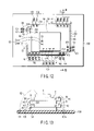
- FIG. 12 is a plan view of a multichip package showing an example of the third embodiment.
- FIG. 13 is a cross-sectional view taken along a line XIII-XIII in FIG. 12 .
- a semiconductor device relates to a multichip package in which a plurality of memory chips are laminated.
- the plurality of memory chip have, e.g., the same structure, and power supply pads, ground pads, and memory pads are provided along two sides (a first side and a second side) perpendicular to each other in four sides of an upper surface of each rectangular or square memory chip.
- At least one power supply pad is provided along each of the first side and the second side, and the single power supply pad on each side is arranged at each diagonal corner of the chip upper surface facing a diagonal line direction.
- the memory chip on an upper layer side is translated and laminated on an upper surface of the memory chip on a lower layer side in such a manner that the respective pads provided on the two sides perpendicular to each other are exposed, i.e., the power supply pad of the memory chip on the lower layer side is not hidden behind the memory chip on the upper layer side as seen from the upper side of the chips.
- the multichip package according to the example of the present invention can avoid a reduction in performance and suppress an increase in a package size of the multichip package.
- FIG. 1 is a plan view of a multichip package according to the first embodiment. Additionally, FIG. 2 is a cross-sectional view taken along a line II-II in FIG. 1 .
- a package substrate 100 is, e.g., an insulating substrate having an electroconductive wiring layer formed on a surface thereof.
- substrate power supply pads 101 On the surface of the package substrate 100 are provided substrate power supply pads 101 , substrate ground pads 102 , substrate memory pads 103 , and substrate controller pads 104 , respectively.
- external terminals are provided at an outer edge portion or on a rear surface of the package substrate 100 , but they are omitted in the drawing in this embodiment.
- the external terminals are, e.g., a lead frame electrically connected with the outer edge portion, a ball grid array (BGA) electrically connected with the rear surface of the package substrate 1 , and others.
- BGA ball grid array
- a wiring layer that connects the external terminals with respective pads 101 , 102 , 103 , and 104 on the package substrate 100 is also provided on the surface of the package substrate 100 , but this layer is also omitted in the drawing like the external terminals.
- a first memory chip 1 is arranged on the package substrate (the insulating substrate) 100 .
- Power supply pads 11 A and 11 B, ground pads 12 A and 12 B, and a plurality of memory pads 13 are arranged on an upper surface of the first memory chip 1 . These pads 11 A, 11 B, 12 A, 12 B, and 13 are formed of an electroconductive material.
- At least one power supply pad 11 A or 11 B is provided on the upper surface of the first memory chip 1 along each of first and second sides A 1 and B 1 of the upper side of the first memory chip perpendicular to each other. It is to be noted that first side A 1 is, e.g., a side whose length is longer that a length of second side B 1 .
- the two power supply pads 11 A and 11 B are arranged at diagonal corners of the upper surface of the memory chip 1 , respectively. Moreover, power supply pads 11 A and 11 B supply a power supply voltage that is required to drive the first memory chip 1 .
- Ground pads 12 A and 12 B are arranged at the diagonal corners of the upper surface of the memory chip 1 in such a manner that they are adjacent to power supply pads 11 A and 11 B along first side A 1 and second side B 1 , respectively. Ground pads 12 A and 12 B supply a ground voltage serving as a reference potential.
- power supply pad 11 A and ground pad 12 A may be provided on the memory chip 1 in such a manner that they are arranged in an opposite pattern. This can be likewise applied to power supply pad 11 B and ground pad 12 B.
- the plurality of memory pads 13 are arranged along, e.g., first side A 1 .
- the memory pads 13 are constituted of a control signal pad, an input/output signal pad, and an address pad, and they are arranged in an arbitrary pattern. It is to be noted that the memory pads 13 may be provided along side B 1 .
- a second memory chip 2 is arranged on the first memory chip 1 .
- the second memory chip 2 is, e.g., a memory chip having substantially the same configuration as the first memory chip 1 . Therefore, on an upper surface of the second memory chip 2 are provided power supply pads 21 A and 21 B, ground pads 22 A and 22 B, and a plurality of memory pads 23 in the same arrangement as the respective pads on the first memory chip 1 along first and second sides A 2 and B 2 of the second memory chip 2 .
- a controller chip 8 is arranged on the second memory chip.
- a size of the controller chip 8 is smaller than sizes of the first and second memory chips 1 and 2 .
- controller pads 81 for a control signal, a data input/output signal, and a power supply/ground voltage.
- the memory chips 1 and 2 and the controller chip 8 are laminated on the package substrate 100 through thin insulating layers (not shown), e.g., an insulating adhesive.
- controller chip 8 does not have to be provided at the uppermost part of the laminate chips, and a multichip package including the memory chips 1 and 2 alone may be adopted.
- FIG. 2 also shows pads and wires on a near side or a far side apart from a cross section taken along a line II-II and these members are indicated by broken lines.
- the substrate power supply pads 101 are connected with power supply pads 11 A and 11 B of the first memory chip 1 and power supply pads 21 A and 21 B of the second memory chip based on wire bonding using wires 14 and 24 , e.g., Au thin lines.
- the substrate ground pads 102 are connected with ground pads 12 A and 12 B of the first memory chip and ground pads 22 A and 22 B of the second memory chip based on wire bonding.
- the substrate memory pads 103 are connected with the memory pads 13 of the first memory chip 1 and the memory pads 23 of the second memory chip 2 based on wire bonding.
- each pad of the second memory chip 2 is connected with each corresponding pad of the first memory chip through the wire 24 to be electrically connected with each pad of the package substrate 100 through the wire 14 extending from the first memory chip as shown in FIGS. 1 and 2 .
- the controller pads 104 are connected with the controller pads 81 through wires 82 .
- the substrate controller pads 104 are constituted of a control signal pad, a data input/output pad, and a power supply pad. It is to be noted that the pads for the power supply and the ground on the controller chip 8 are connected with the pads 104 different from the substrate power supply pads 101 and the substrate ground pads 102 connected with the first and second memory chips as explained in this embodiment. That is because the controller chip 8 operates and a reduction in the power supply voltage and an increase in the ground voltage thereby occur when the power supply and ground pads of the controller chip 8 are connected with pads 101 and 102 as common pads for the first and second memory chips, which adversely affects the operations of the memory chips.
- the number of the pads on the package substrate 100 can be reduced. According to this structure, a pitch between the pads can be widened, and short circuit can be prevented from occurring between the pads or between the wires.
- the second memory chip 2 on the upper layer side is translated and laminated on the first memory chip 1 in such a manner that the first side A 1 and the second side B 1 of the upper surface of the first memory chip 1 on the lower layer side perpendicular to each other are exposed. Therefore, the two chips can be laminated so that the respective pads provided along first and second sides A 1 and B 1 of the first memory chip 1 are exposed.
- wire bonding can be effected along the two sides of each memory chip.
- a direction along which the second memory chip is translated is, e.g., a diagonal direction with respect to the upper surface of the first memory chip 1 . It is to be noted that this translating direction is not restricted to the diagonal direction and it may be a direction along which the first and second sides of the first memory chip on the lower layer side are exposed. Further, a size of a space that is exposed when the second memory chip is translated is a size which enables assuring a space required to perform wire bonding with respect to the pads.
- At least one power supply pad 11 A or 11 B provided on the first memory chip is disposed along each of sides A 1 and B 1 , and the single power supply pad 11 A or 11 B along each side A 1 or B 1 is arranged at each diagonal corner of the upper surface of the memory chip 1 .
- ground pads 12 A and 12 B are arranged to be adjacent to power supply pads 11 A and 11 B, respectively. When ground pads 12 A and 12 B are arranged at the respective diagonal corners on the chip, an increase in the ground voltage can be suppressed.
- the memory chip on the upper layer side is arranged on the memory chip on the lower layer side in such a manner that the two sides of the memory chip on the lower layer side perpendicular to each other are exposed. Therefore, the pads of the memory chip on the lower layer side can be provided along the exposed two sides.
- the power supply pads and the ground pads that supply the power supply voltage and the ground voltage can be provided at the diagonal corners of the upper surface of the memory chip.
- FIGS. 3 and 4 are views showing an example of this embodiment. It is to be noted that like reference numerals denote members equal to those in the basic structure, thereby omitting a detailed explanation thereof.
- respective pads are provided on upper surfaces of first and second memory chips 1 and 2 along their first sides A 1 and A 2 and second sides B 1 and B 2 , respectively.
- the second memory chip 2 is translated with respect to the upper surface of the first memory chip and laminated on the first memory chip 1 in such a manner that the respective pads of the first memory chip provided along sides A 1 and B 1 are exposed.
- first and second memory chips 1 and 2 are, e.g., flash memories.
- This example further includes third and fourth memory chips 3 and 4 besides the first and second memory chips.
- Each of the third and fourth memory chips 3 and 4 is a non-volatile semiconductor memory, e.g., a dynamic random access memory (DRAM).
- DRAM dynamic random access memory
- Respective pads of the third and fourth memory chips 3 and 4 are provided on upper surfaces of the respective chips along two sides perpendicular to each other like the first and second memory chips 1 and 2 .
- power supply pads 31 A and 31 B, ground pads 32 A and 32 B, and a plurality of memory pads 33 are provided on an upper surface of the third memory chip 3 .
- At least one power supply pad 31 A or 31 B is provided on the upper surface of the chip 3 along each of sides A 3 and B 3 . Further, the single power supply pad 31 A or 31 B on each of sides A 3 and B 3 is provided at each diagonal corner of the upper surface of the memory chip 3 .
- Ground pads 32 A and 32 B are provided to be adjacent to power supply pads 31 A and 31 B along sides A 3 and B 3 , respectively.
- the plurality of memory pads 33 are provided on the upper surface of the chip 3 along side A 3 of the third memory chip.
- the fourth memory chip 4 has the same structure as the third memory chip 3 , and power supply pads 41 A and 41 B, ground pads 42 A and 42 B, and memory pads 43 are provided on an upper surface of the chip 4 along sides A 4 and B 4 , respectively.
- each of the third and fourth memory chips 3 and 4 may be a flash memory like the first and second memory chips.
- the memory chips are electrically connected with a package substrate 100 through the respective memory chips on a lower layer side.
- the third memory chip 3 is laminated on the second memory chip in such a manner that the respective pads provided on the upper surface of the second memory chip along the two side shown in FIGS. 1 and 2 are exposed.
- the fourth memory chip 4 is laminated on the third memory chip 3 in such a manner that the respective pads on the upper surface of the third memory chip along the two sides A 3 and B 3 are exposed.
- the memory chips in two or more layers can be laminated. Therefore, the storage capacity of the multichip package can be increased.
- the storage capacity of the multichip package can be increased.
- the order of laminating the memory chips is not restricted to the above-explained order, and a volatile memory chip may be arranged on the lower layer side of a non-volatile memory chip.
- the memory chips may be laminated in four or more layers.
- the plurality of memory chips are laminated in this example, a plurality of LSI chips may be laminated, or both memory chips and LSI chips may be laminated.
- the memory chip on the upper layer side in the plurality of memory chips constituting the multichip package is translated and laminated in such a manner that the two sides of the upper surface of the memory chip on the lower layer side perpendicular to each other are exposed.
- arranging the power supply pads of the memory chip at the diagonal corners of the chip upper surface enables avoiding degradation in performance of the chip due to the internal wiring resistance.
- the memory chips according to this embodiment have the same structure as the memory chips explained in the first embodiment, and the same effect as that described above can be obtained. Further, like reference numerals denote like members, thereby omitting a detailed explanation thereof.
- a second memory chip 2 is laminated on a first memory chip 1 in such a manner that respective pads of the first memory chip 1 provided along a side A 1 and a side B 1 are exposed.
- a spacer 9 formed of an insulator is provided on the second memory chip 2 .
- a thickness of this spacer 9 is a thickness that enables assuring a space in a thickness direction for wire bonding of the second memory chip 2 .
- a third memory chip 3 is arranged on the second memory chip 2 through the spacer 9 .
- This third memory chip 3 is translated with respect to the second memory chip 2 in a direction opposite to a translating direction of the second memory chip 2 .
- the third memory chip 3 is arranged at a position where it substantially overlaps the first memory chip 1 . Specifically, the third memory chip 3 is arranged at a position where a first side A 3 of the memory chip 3 substantially overlaps the first side A 1 of the first memory chip 1 and a second side B 3 of the memory chip 3 substantially overlaps the second side B 1 of the first memory chip 1 .
- a fourth memory chip 4 is translated in such a manner that respective pads of the third memory chip 3 provided along the side A 3 and the side B 3 are exposed. Moreover, the fourth memory chip 4 is arranged at a position where it substantially overlaps the second memory chip 2 .
- the memory chip (the fourth memory chip 4 ) in the uppermost layer is translated for the same distance as the second memory chip.
- wire bonding of the above-explained structure is carried out as follows.
- the respective pads of the first memory chip 1 are connected with a package substrate 100 through wires 14 .
- the respective pads of the second memory chip 2 are connected with the pads of the first memory chip through wires 24 .
- the respective pads of the third memory chip 3 are connected with the package substrate 100 through wires 34 .
- the respective pads of the fourth memory chip 4 are connected with the respective pads of the third memory chip through wires 44 .
- the second memory chip 2 is connected with the package substrate 100 through the first memory chip 1 . Further, the fourth memory chip 4 is connected with the package substrate 100 via the third memory chip 3 .
- a size of the multichip package can be set within a size including the translated second memory chip 2 .
- the multichip package according to this embodiment can be manufactured in a size including the translated second memory chip 2 even if the plurality of memory chips are laminated.
- the multichip package in which the four memory chips are laminated has been explained in this embodiment.
- the present invention is not restricted thereto, and it is possible to adopt a structure where the three memory chips are laminated without laminating the fourth memory chip or a structure where a spacer is further provided on the fourth memory chip and another memory chip is further laminated thereon.
- using the spacer suppresses a size of the multichip package in a plane direction from being increased in the translating direction of the memory chip when laminating the plurality of memory chips to increase a capacity.
- the spacer assures a space in a thickness direction required for wire bonding of the chip provided on the lower layer side of this spacer. Therefore, in the second embodiment, the thickness of this spacer increases the thickness of the multichip package.
- FIGS. 7 and 8 are views showing a structure of a multichip package according to this embodiment. It is to be noted that memory chips according to this embodiment have the same structures as the memory chips according to the first embodiment, thereby obtaining the same effect. Furthermore, like reference numerals denote like members, thus omitting a detailed explanation thereof.
- a plurality of memory chips 1 , 2 , and 3 and a controller chip 8 are laminated on a package substrate 100 . That is, the second memory chip 2 is arranged between the first memory chip 1 and the third memory chip 3 .
- This second memory chip 2 is symmetrical in a lateral direction with respect to the first and third memory chips 1 and 3 , translated on an upper surface of the first memory chip 1 in such a manner that two sides A 1 and B 1 on which pads of the first memory chip 1 are provided are exposed, and arranged on the memory chip 1 .
- FIGS. 7 and 8 The structure depicted in FIGS. 7 and 8 will now be explained in stages with reference to FIGS. 9 and 11 . It is to be noted that wires will be omitted in the drawings.
- the first memory chip 1 is provided on a package substrate 100 .
- the second memory chip 2 is rotated 180° with respect to the first memory chip 1 , and arranged to be flipped horizontally. Specifically, a first side A 2 where pads of the second memory chip 2 are provided is placed to be opposed to a position of a first side A 1 where pads of the first memory chip 1 are provided. Furthermore, a second side B 2 where pads of the second memory chip 2 are provided is placed to be opposed to a position of a second side B 1 where pads of the first memory chip 1 are provided.
- the second memory chip 2 is translated and arranged with respect to an upper surface of the first memory chip 1 in such a manner that the respective pads provided on upper surfaces of the first memory chip 1 along the two sides A 1 and B 2 perpendicular to each other are exposed.
- the third memory chip 3 is opposite to the second memory chip 2 in the lateral direction, and it is translated on an upper surface of the second memory chip 2 in a direction opposite to the translating direction of the second memory chip 2 and arranged on the second memory chip 2 .
- the third memory chip 3 is arranged at a position where side A 3 of the third memory chip 3 substantially overlaps side A 1 of the first memory chip 1 and side B 3 of the third memory chip 3 substantially overlaps side B 1 of the first memory chip 1 .
- substrate power supply pads 101 , substrate ground pads 102 , and memory pads 103 are provided on the package substrate 100 along first sides A 1 and A 3 and second sides B 1 and B 3 of memory chips 1 and 3 and first side A 2 and second side B 2 of memory chip 2 . That is, these pads 101 , 102 , and 103 are arranged on the package substrate 100 to surround the peripheries of laminated memory chips 1 , 2 , and 3 , and wire bonding between the pads of the respective memory chips is formed without becoming complicated.
- a fourth memory chip 4 is arranged on the third memory chip 3 .
- each of the first to fourth memory chips 1 , 2 , 3 and 4 may be either a volatile semiconductor memory chip or a non-volatile semiconductor memory chip, or both the volatile memory chip and the non-volatile memory chip may be used.
- the fourth memory chip 4 has the same configuration as the first to third memory chips 1 , 2 , and 3 , and has pads arranged thereon.
- two pairs of power supply pads 41 A and 41 B are provided on an upper surface of the fourth memory chip 4 along side A 4 and side B 4 , respectively.
- the two pairs of power supply pads 41 A and 41 B are arranged at diagonal corners of the upper surface of the memory chip 4 .
- a plurality of memory pads 43 are provided on the upper surface of the fourth memory chip 4 along first side A 1 of the fourth memory chip 4 .
- the fourth memory chip 4 is opposite to the third memory chip 3 in a lateral direction, and it is translated in a direction opposite to the translating direction of the third memory chip 3 in such a manner that the respective pads provided along the two sides A 3 , B 3 of the third memory chip 3 perpendicular to each other are exposed.
- the fourth memory chip 4 is arranged at a position where side A 4 of the fourth memory chip 4 substantially overlaps side A 2 of the second memory chip 2 and side B 4 of the fourth memory chip 4 substantially overlaps side B 2 of the second memory chip 2 .
- the plurality of memory chips can be laminated, an increase in the multipackage size caused due to a spacer can be avoided, and a storage capacity can be increased.
- the multichip package having the four-layer structure has been explained in this example, but the memory chips may be laminated in four or more layers. Furthermore, although the plurality of memory chips are laminated in this example, a plurality of LSI chips may be laminated, or both memory chips and LSI memory chips may be laminated.
- the semiconductor device according to the examples of the present invention is applied to portable electronic devices, e.g., a mobile phone or a digital camera.
- the examples of the present invention can avoid degradation of performance of the memory chips constituting the multichip package and suppress an increase in the size of the package.
Landscapes
- Semiconductor Memories (AREA)
- Dram (AREA)
Abstract
Description
- This application is based upon and claims the benefit of priority from prior Japanese Patent Application No. 2006-317523, filed Nov. 24, 2006, the entire contents of which are incorporated herein by reference.
- 1. Field of the Invention
- The present invention relates to a semiconductor device, and more particularly to a multichip package.
- 2. Description of the Related Art
- For example, a demand for miniaturization of a package of a portable electronic device as typified by a mobile phone has been swiftly increased because of its characteristics.
- Therefore, a multichip package (MCP) technology of laminating a plurality of semiconductor chips on an insulating substrate to be formed as one package is used.
- In particular, when a memory chip, e.g., a random access memory (RAM) or a flash memory and a controller chip thereof are packaged based on the MCP technology, since a higher capacity of a memory is preferable, the plurality of memory chips are laminated in many cases.
- Since electroconductive pads are respectively provided on a package substrate, a memory chip, and a controller chip, these members are electrically connected with each other by connecting their pads through bonding wires.
- Therefore, each chip is laminated while assuring a space where wire bonding can be effected near the pad provided on each chip.
- In the multichip package, since the memory chips to be laminated usually have substantially the same size, when these memory chips are simply laminated, the pad on a chip that is arranged on a lower layer side is not exposed, and wire bonding cannot be performed.
- Therefore, a multichip package in which pads are provided along one or two sides of each memory chip and the chips are laminated in a zigzag pattern so that the pads on the respective chips are exposed has been proposed (see, e.g., JP-A 2004-221215 [KOKAI]).
- However, when a power supply pad that supplies a power supply voltage or a ground pad that supplies a ground voltage is arranged while being biased to one side of each memory chip surface, a voltage distribution in each chip becomes non-uniform. That is because a power supply voltage and a ground voltage are supplied to a region apart from the pad of such a chip through wiring lines in each chip, an internal wiring resistance thereof is generally large, and an influence of a drop in voltage becomes larger as distanced from the pad.
- Therefore, when a consumption current is increased, a reduction in the power supply voltage and an increase in the ground voltage in the region apart from the bonded pad cannot be suppressed because of the internal wiring resistance, thereby decreasing performance of each memory chip.
- Further, since the plurality of memory chips are laminated while being staggered in the same direction so that a pad region of each chip is exposed, a package size becomes large in a staggering direction.
- An aspect of a semiconductor device comprising: a package substrate which has a plurality of pads to which a power supply voltage is supplied on an upper surface thereof; a first memory chip which is arranged on the package substrate and has a first power supply pad provided on a first side and a second power supply pad provided on a second side perpendicular to the first side; and a second memory chip which is translated in a direction along which the first and second power supply pads of the first memory chip are exposed, and arranged on the first memory chip, wherein the first and second power supply pads are provided at diagonal corners of the first memory chip, respectively.
- An aspect of a semiconductor device comprising: a package substrate which has a plurality of pads to which a power supply voltage is supplied on an upper surface thereof; a first memory chip which is arranged on the package substrate and has a first power supply pad provided on a first side and a second power supply pad provided on a second side perpendicular to the first side; a second memory chip which is translated in a direction along which the first and second power supply pads of the first memory chip are exposed, and arranged on the first memory chip; and a third memory chip which is translated in a direction opposite to the translating direction of the second memory chip, and arranged on the second memory chip through a spacer at a position where it overlaps the first memory chip, wherein the first and second power supply pads are provided at diagonal corners of the first memory chip, respectively.
- An aspect of a semiconductor device comprising: a package substrate; a first memory chip which is arranged on the package substrate and has a first power supply pad provided on a first side and a second power supply pad provided on a second side perpendicular to the first side; a second memory chip which is opposite to the first memory chip in a lateral direction, translated in a direction along which the first and second power supply pads of the first memory chip are exposed, and arranged on the first memory chip; and a third memory chip which is translated in a direction opposite to the translating direction of the second memory chip and arranged on the second memory chip, wherein the first and second power supply pads are provided at diagonal corners of the first memory chip, respectively.
-
FIG. 1 is a plan view of a multichip package showing a basic configuration of a first embodiment; -
FIG. 2 is a cross-sectional view taken along a line II-II inFIG. 1 ; -
FIG. 3 is a plan view of a multichip package showing an application example of the first embodiment; -
FIG. 4 is a cross-sectional view taken along a line IV-IV inFIG. 3 ; -
FIG. 5 is a plan view of a multichip package showing a configuration of a second embodiment; -
FIG. 6 is a cross-sectional view taken along a line VI-VI inFIG. 5 ; -
FIG. 7 is a plan view of a multichip package showing a basic configuration of a third embodiment; -
FIG. 8 is a cross-sectional view taken along a line VIII-VIII inFIG. 7 ; -
FIG. 9 is a plan view showing a configuration depicted inFIG. 7 in stages; -
FIG. 10 is a plan view showing the configuration depicted inFIG. 7 in stages; -
FIG. 11 is a plan view showing the configuration depicted inFIG. 7 in stages; -
FIG. 12 is a plan view of a multichip package showing an example of the third embodiment; and -
FIG. 13 is a cross-sectional view taken along a line XIII-XIII inFIG. 12 . - Several embodiments for carrying out the present invention will now be explained hereinafter in detail with reference to the accompanying drawings.
- A semiconductor device according to an example of the present invention relates to a multichip package in which a plurality of memory chips are laminated.
- The plurality of memory chip have, e.g., the same structure, and power supply pads, ground pads, and memory pads are provided along two sides (a first side and a second side) perpendicular to each other in four sides of an upper surface of each rectangular or square memory chip.
- Furthermore, at least one power supply pad is provided along each of the first side and the second side, and the single power supply pad on each side is arranged at each diagonal corner of the chip upper surface facing a diagonal line direction.
- When such a memory chip is laminated, the following basic structure is provided. That is, the memory chip on an upper layer side is translated and laminated on an upper surface of the memory chip on a lower layer side in such a manner that the respective pads provided on the two sides perpendicular to each other are exposed, i.e., the power supply pad of the memory chip on the lower layer side is not hidden behind the memory chip on the upper layer side as seen from the upper side of the chips.
- As a result, a voltage drop due to an internal wiring resistance of each chip can be alleviated.
- Therefore, the multichip package according to the example of the present invention can avoid a reduction in performance and suppress an increase in a package size of the multichip package.
- Moreover, a configuration of the multichip package based on the basic structure will be also explained hereinafter. Thus, a technology that can suppress an increase in the package size and increase a memory capacity of the multichip package is proposed.
-
FIG. 1 is a plan view of a multichip package according to the first embodiment. Additionally,FIG. 2 is a cross-sectional view taken along a line II-II inFIG. 1 . - A
package substrate 100 is, e.g., an insulating substrate having an electroconductive wiring layer formed on a surface thereof. - On the surface of the
package substrate 100 are provided substratepower supply pads 101,substrate ground pads 102,substrate memory pads 103, andsubstrate controller pads 104, respectively. It is to be noted that external terminals are provided at an outer edge portion or on a rear surface of thepackage substrate 100, but they are omitted in the drawing in this embodiment. The external terminals are, e.g., a lead frame electrically connected with the outer edge portion, a ball grid array (BGA) electrically connected with the rear surface of thepackage substrate 1, and others. - Further, although a wiring layer that connects the external terminals with
respective pads package substrate 100 is also provided on the surface of thepackage substrate 100, but this layer is also omitted in the drawing like the external terminals. - A
first memory chip 1 is arranged on the package substrate (the insulating substrate) 100. -
Power supply pads ground pads memory pads 13 are arranged on an upper surface of thefirst memory chip 1. Thesepads - At least one
power supply pad first memory chip 1 along each of first and second sides A1 and B1 of the upper side of the first memory chip perpendicular to each other. It is to be noted that first side A1 is, e.g., a side whose length is longer that a length of second side B1. - Furthermore, the two
power supply pads memory chip 1, respectively. Moreover,power supply pads first memory chip 1. -
Ground pads memory chip 1 in such a manner that they are adjacent topower supply pads Ground pads - It is to be noted that
power supply pad 11A andground pad 12A may be provided on thememory chip 1 in such a manner that they are arranged in an opposite pattern. This can be likewise applied topower supply pad 11B andground pad 12B. - Additionally, the plurality of
memory pads 13 are arranged along, e.g., first side A1. Thememory pads 13 are constituted of a control signal pad, an input/output signal pad, and an address pad, and they are arranged in an arbitrary pattern. It is to be noted that thememory pads 13 may be provided along side B1. - A
second memory chip 2 is arranged on thefirst memory chip 1. Thesecond memory chip 2 is, e.g., a memory chip having substantially the same configuration as thefirst memory chip 1. Therefore, on an upper surface of thesecond memory chip 2 are providedpower supply pads ground pads memory pads 23 in the same arrangement as the respective pads on thefirst memory chip 1 along first and second sides A2 and B2 of thesecond memory chip 2. - A
controller chip 8 is arranged on the second memory chip. A size of thecontroller chip 8 is smaller than sizes of the first andsecond memory chips - On a surface of the
controller chip 8 are providedcontroller pads 81 for a control signal, a data input/output signal, and a power supply/ground voltage. - The
memory chips controller chip 8 are laminated on thepackage substrate 100 through thin insulating layers (not shown), e.g., an insulating adhesive. - It is to be noted that the
controller chip 8 does not have to be provided at the uppermost part of the laminate chips, and a multichip package including thememory chips - The respective pads provided on the
package substrate 100, the first andsecond memory chips controller chip 8 are connected with each other as follows. It is to be noted thatFIG. 2 also shows pads and wires on a near side or a far side apart from a cross section taken along a line II-II and these members are indicated by broken lines. - The substrate
power supply pads 101 are connected withpower supply pads first memory chip 1 andpower supply pads bonding using wires - The
substrate ground pads 102 are connected withground pads ground pads - Moreover, the
substrate memory pads 103 are connected with thememory pads 13 of thefirst memory chip 1 and thememory pads 23 of thesecond memory chip 2 based on wire bonding. - It is to be noted that each pad of the
second memory chip 2 is connected with each corresponding pad of the first memory chip through thewire 24 to be electrically connected with each pad of thepackage substrate 100 through thewire 14 extending from the first memory chip as shown inFIGS. 1 and 2 . - When the chips are connected with each other in this manner, complicated wire bonding does not have to be carried out, and a parasitic capacitance of the wire bonded between pads having a large step can be suppressed.
- The
controller pads 104 are connected with thecontroller pads 81 throughwires 82. Thesubstrate controller pads 104 are constituted of a control signal pad, a data input/output pad, and a power supply pad. It is to be noted that the pads for the power supply and the ground on thecontroller chip 8 are connected with thepads 104 different from the substratepower supply pads 101 and thesubstrate ground pads 102 connected with the first and second memory chips as explained in this embodiment. That is because thecontroller chip 8 operates and a reduction in the power supply voltage and an increase in the ground voltage thereby occur when the power supply and ground pads of thecontroller chip 8 are connected withpads controller chip 8 are connected with the substratepower supply pads 101 and thesubstrate ground pads 102 connected with the first and second memory chips, the number of the pads on thepackage substrate 100 can be reduced. According to this structure, a pitch between the pads can be widened, and short circuit can be prevented from occurring between the pads or between the wires. - In the above-explained multichip package, as shown in
FIGS. 1 and 2 , thesecond memory chip 2 on the upper layer side is translated and laminated on thefirst memory chip 1 in such a manner that the first side A1 and the second side B1 of the upper surface of thefirst memory chip 1 on the lower layer side perpendicular to each other are exposed. Therefore, the two chips can be laminated so that the respective pads provided along first and second sides A1 and B1 of thefirst memory chip 1 are exposed. - Accordingly, wire bonding can be effected along the two sides of each memory chip.
- A direction along which the second memory chip is translated is, e.g., a diagonal direction with respect to the upper surface of the
first memory chip 1. It is to be noted that this translating direction is not restricted to the diagonal direction and it may be a direction along which the first and second sides of the first memory chip on the lower layer side are exposed. Further, a size of a space that is exposed when the second memory chip is translated is a size which enables assuring a space required to perform wire bonding with respect to the pads. - Furthermore, as explained above, at least one
power supply pad power supply pad memory chip 1. - For example, when
power supply pads first memory chip 1 becomes non-uniform, and performance of thememory chip 1 is decreased. - However, when the power supply pads are provided at the respective diagonal corners of the memory chip like this embodiment, an influence of a voltage drop due to the internal wiring resistance can be alleviated, and the power supply voltage can be supplied to provide a further uniform voltage distribution in the memory chip. Furthermore,
ground pads power supply pads ground pads - Therefore, a reduction in performance of the memory chip due to the internal wiring resistance of the memory chip can be avoided.
- As explained above, in the multichip package in which the plurality of memory chips are laminated, the memory chip on the upper layer side is arranged on the memory chip on the lower layer side in such a manner that the two sides of the memory chip on the lower layer side perpendicular to each other are exposed. Therefore, the pads of the memory chip on the lower layer side can be provided along the exposed two sides.
- Accordingly, the power supply pads and the ground pads that supply the power supply voltage and the ground voltage can be provided at the diagonal corners of the upper surface of the memory chip.
- Therefore, in a region apart from the pads, a reduction in the power supply voltage and an increase in the ground voltage due to the internal wiring resistance in each chip can be suppressed.
- Thus, a reduction in performance of the multichip package can be avoided.
-
FIGS. 3 and 4 are views showing an example of this embodiment. It is to be noted that like reference numerals denote members equal to those in the basic structure, thereby omitting a detailed explanation thereof. - As explained in the section of the basic structure, respective pads are provided on upper surfaces of first and
second memory chips - Additionally, the
second memory chip 2 is translated with respect to the upper surface of the first memory chip and laminated on thefirst memory chip 1 in such a manner that the respective pads of the first memory chip provided along sides A1 and B1 are exposed. - These first and
second memory chips - This example further includes third and
fourth memory chips - Each of the third and
fourth memory chips - Respective pads of the third and
fourth memory chips second memory chips - That is,
power supply pads ground pads memory pads 33 are provided on an upper surface of thethird memory chip 3. - At least one
power supply pad chip 3 along each of sides A3 and B3. Further, the singlepower supply pad memory chip 3. -
Ground pads power supply pads - Furthermore, the plurality of
memory pads 33 are provided on the upper surface of thechip 3 along side A3 of the third memory chip. - The
fourth memory chip 4 has the same structure as thethird memory chip 3, andpower supply pads ground pads memory pads 43 are provided on an upper surface of thechip 4 along sides A4 and B4, respectively. - It is to be noted that each of the third and
fourth memory chips - Moreover, the memory chips are electrically connected with a
package substrate 100 through the respective memory chips on a lower layer side. - As shown in
FIGS. 3 and 4 , thethird memory chip 3 is laminated on the second memory chip in such a manner that the respective pads provided on the upper surface of the second memory chip along the two side shown inFIGS. 1 and 2 are exposed. - Additionally, the
fourth memory chip 4 is laminated on thethird memory chip 3 in such a manner that the respective pads on the upper surface of the third memory chip along the two sides A3 and B3 are exposed. - As shown in this example, the memory chips in two or more layers can be laminated. Therefore, the storage capacity of the multichip package can be increased.
- Accordingly, in addition to the effect explained in the section of the basic structure, the storage capacity of the multichip package can be increased.
- Further, it is possible to provide a multichip package in which different types of memory chips like a non-volatile memory and a volatile memory can be laminated and a plurality of different types of memory chips are included.
- It is to be noted that the order of laminating the memory chips is not restricted to the above-explained order, and a volatile memory chip may be arranged on the lower layer side of a non-volatile memory chip. Furthermore, although the multichip package having the four-layer structure has been explained in this example, the memory chips may be laminated in four or more layers. Moreover, although the plurality of memory chips are laminated in this example, a plurality of LSI chips may be laminated, or both memory chips and LSI chips may be laminated.
- In the first embodiment, the memory chip on the upper layer side in the plurality of memory chips constituting the multichip package is translated and laminated in such a manner that the two sides of the upper surface of the memory chip on the lower layer side perpendicular to each other are exposed.
- Additionally, arranging the power supply pads of the memory chip at the diagonal corners of the chip upper surface enables avoiding degradation in performance of the chip due to the internal wiring resistance.
- However, when the plurality of memory chips are laminated to increase a capacity of the memory, a size of the package becomes large in a direction along which the memory chip is translated.
- Thus, in the second embodiment, a structure of a multichip package that solves this problem will be explained. It is to be noted that the memory chips according to this embodiment have the same structure as the memory chips explained in the first embodiment, and the same effect as that described above can be obtained. Further, like reference numerals denote like members, thereby omitting a detailed explanation thereof.
- As shown in
FIGS. 5 and 6 , asecond memory chip 2 is laminated on afirst memory chip 1 in such a manner that respective pads of thefirst memory chip 1 provided along a side A1 and a side B1 are exposed. - A
spacer 9 formed of an insulator is provided on thesecond memory chip 2. A thickness of thisspacer 9 is a thickness that enables assuring a space in a thickness direction for wire bonding of thesecond memory chip 2. - A
third memory chip 3 is arranged on thesecond memory chip 2 through thespacer 9. Thisthird memory chip 3 is translated with respect to thesecond memory chip 2 in a direction opposite to a translating direction of thesecond memory chip 2. - Furthermore, the
third memory chip 3 is arranged at a position where it substantially overlaps thefirst memory chip 1. Specifically, thethird memory chip 3 is arranged at a position where a first side A3 of thememory chip 3 substantially overlaps the first side A1 of thefirst memory chip 1 and a second side B3 of thememory chip 3 substantially overlaps the second side B1 of thefirst memory chip 1. - A
fourth memory chip 4 is translated in such a manner that respective pads of thethird memory chip 3 provided along the side A3 and the side B3 are exposed. Moreover, thefourth memory chip 4 is arranged at a position where it substantially overlaps thesecond memory chip 2. - That is, the memory chip (the fourth memory chip 4) in the uppermost layer is translated for the same distance as the second memory chip.
- Additionally, wire bonding of the above-explained structure is carried out as follows.
- The respective pads of the
first memory chip 1 are connected with apackage substrate 100 throughwires 14. The respective pads of thesecond memory chip 2 are connected with the pads of the first memory chip throughwires 24. - The respective pads of the
third memory chip 3 are connected with thepackage substrate 100 throughwires 34. The respective pads of thefourth memory chip 4 are connected with the respective pads of the third memory chip throughwires 44. - That is, the
second memory chip 2 is connected with thepackage substrate 100 through thefirst memory chip 1. Further, thefourth memory chip 4 is connected with thepackage substrate 100 via thethird memory chip 3. - As explained above, in this embodiment, a size of the multichip package can be set within a size including the translated
second memory chip 2. - Therefore, the multichip package according to this embodiment can be manufactured in a size including the translated
second memory chip 2 even if the plurality of memory chips are laminated. - Accordingly, a reduction in performance of the multichip package can be avoided, and an increase in the package size of the multichip package can be suppressed. A storage capacity of the multichip package can be thereby increased.
- It is to be noted that the multichip package in which the four memory chips are laminated has been explained in this embodiment. However, the present invention is not restricted thereto, and it is possible to adopt a structure where the three memory chips are laminated without laminating the fourth memory chip or a structure where a spacer is further provided on the fourth memory chip and another memory chip is further laminated thereon.
- In the structure of the multichip package according to the second embodiment, using the spacer suppresses a size of the multichip package in a plane direction from being increased in the translating direction of the memory chip when laminating the plurality of memory chips to increase a capacity.
- However, adopting the spacer assures a space in a thickness direction required for wire bonding of the chip provided on the lower layer side of this spacer. Therefore, in the second embodiment, the thickness of this spacer increases the thickness of the multichip package.
- A structure of a multichip package that solves this problem will now be explained hereinafter.
-
FIGS. 7 and 8 are views showing a structure of a multichip package according to this embodiment. It is to be noted that memory chips according to this embodiment have the same structures as the memory chips according to the first embodiment, thereby obtaining the same effect. Furthermore, like reference numerals denote like members, thus omitting a detailed explanation thereof. - A plurality of
memory chips controller chip 8 are laminated on apackage substrate 100. That is, thesecond memory chip 2 is arranged between thefirst memory chip 1 and thethird memory chip 3. - This
second memory chip 2 is symmetrical in a lateral direction with respect to the first andthird memory chips first memory chip 1 in such a manner that two sides A1 and B1 on which pads of thefirst memory chip 1 are provided are exposed, and arranged on thememory chip 1. - The structure depicted in
FIGS. 7 and 8 will now be explained in stages with reference toFIGS. 9 and 11 . It is to be noted that wires will be omitted in the drawings. - As shown in
FIG. 9 , thefirst memory chip 1 is provided on apackage substrate 100. - Further, as shown in
FIG. 10 , thesecond memory chip 2 is rotated 180° with respect to thefirst memory chip 1, and arranged to be flipped horizontally. Specifically, a first side A2 where pads of thesecond memory chip 2 are provided is placed to be opposed to a position of a first side A1 where pads of thefirst memory chip 1 are provided. Furthermore, a second side B2 where pads of thesecond memory chip 2 are provided is placed to be opposed to a position of a second side B1 where pads of thefirst memory chip 1 are provided. - Moreover, the
second memory chip 2 is translated and arranged with respect to an upper surface of thefirst memory chip 1 in such a manner that the respective pads provided on upper surfaces of thefirst memory chip 1 along the two sides A1 and B2 perpendicular to each other are exposed. - As shown in
FIG. 11 , thethird memory chip 3 is opposite to thesecond memory chip 2 in the lateral direction, and it is translated on an upper surface of thesecond memory chip 2 in a direction opposite to the translating direction of thesecond memory chip 2 and arranged on thesecond memory chip 2. - Additionally, the
third memory chip 3 is arranged at a position where side A3 of thethird memory chip 3 substantially overlaps side A1 of thefirst memory chip 1 and side B3 of thethird memory chip 3 substantially overlaps side B1 of thefirst memory chip 1. - In case of the above-explained structure, substrate
power supply pads 101,substrate ground pads 102, andmemory pads 103 are provided on thepackage substrate 100 along first sides A1 and A3 and second sides B1 and B3 ofmemory chips memory chip 2. That is, thesepads package substrate 100 to surround the peripheries oflaminated memory chips - Therefore, using the above-explained basic structure enables eliminating a need for arrangement of a spacer between the memory chips to be laminated and suppressing an increase in a size of the multichip package in a thickness direction.
- An example of the above-explained structure will now be explained.
- It is to be noted that like reference numerals denote like members, thereby omitting a detailed explanation thereof.
- As shown in
FIGS. 12 and 13 , besides the multichip package explained in the section of the basic structure, afourth memory chip 4 is arranged on thethird memory chip 3. - It is to be noted that each of the first to
fourth memory chips - The
fourth memory chip 4 has the same configuration as the first tothird memory chips - Therefore, two pairs of
power supply pads fourth memory chip 4 along side A4 and side B4, respectively. - Additionally, the two pairs of
power supply pads memory chip 4. Further, a plurality ofmemory pads 43 are provided on the upper surface of thefourth memory chip 4 along first side A1 of thefourth memory chip 4. - The
fourth memory chip 4 is opposite to thethird memory chip 3 in a lateral direction, and it is translated in a direction opposite to the translating direction of thethird memory chip 3 in such a manner that the respective pads provided along the two sides A3, B3 of thethird memory chip 3 perpendicular to each other are exposed. - Furthermore, the
fourth memory chip 4 is arranged at a position where side A4 of thefourth memory chip 4 substantially overlaps side A2 of thesecond memory chip 2 and side B4 of thefourth memory chip 4 substantially overlaps side B2 of thesecond memory chip 2. - As explained above, in the structure according to this example, the plurality of memory chips can be laminated, an increase in the multipackage size caused due to a spacer can be avoided, and a storage capacity can be increased.
- Therefore, a reduction in performance of the multichip package can be avoided, and the package size of the multichip package can be suppressed from being increased. The storage capacity of the multichip package can be thereby increased.
- It is to be noted that the multichip package having the four-layer structure has been explained in this example, but the memory chips may be laminated in four or more layers. Furthermore, although the plurality of memory chips are laminated in this example, a plurality of LSI chips may be laminated, or both memory chips and LSI memory chips may be laminated.
- The semiconductor device according to the examples of the present invention is applied to portable electronic devices, e.g., a mobile phone or a digital camera.
- The examples of the present invention can avoid degradation of performance of the memory chips constituting the multichip package and suppress an increase in the size of the package.
- Additional advantages and modifications will readily occur to those skilled in the art. Therefore, the invention in its broader aspects is not limited to the specific details and representative embodiments shown and described herein. Accordingly, various modifications may be made without departing from the spirit or scope of the general inventive concept as defined by the appended claims and their equivalents.
Claims (20)
Applications Claiming Priority (2)
| Application Number | Priority Date | Filing Date | Title |
|---|---|---|---|
| JP2006317523A JP4921937B2 (en) | 2006-11-24 | 2006-11-24 | Semiconductor integrated circuit |
| JP2006-317523 | 2006-11-24 |
Publications (2)
| Publication Number | Publication Date |
|---|---|
| US20080122064A1 true US20080122064A1 (en) | 2008-05-29 |
| US7683491B2 US7683491B2 (en) | 2010-03-23 |
Family
ID=39462805
Family Applications (1)
| Application Number | Title | Priority Date | Filing Date |
|---|---|---|---|
| US11/943,142 Active 2027-11-25 US7683491B2 (en) | 2006-11-24 | 2007-11-20 | Semiconductor device |
Country Status (2)
| Country | Link |
|---|---|
| US (1) | US7683491B2 (en) |
| JP (1) | JP4921937B2 (en) |
Cited By (10)
| Publication number | Priority date | Publication date | Assignee | Title |
|---|---|---|---|---|
| US20100078790A1 (en) * | 2008-09-29 | 2010-04-01 | Hitachi, Ltd. | Semiconductor device |
| US20100117214A1 (en) * | 2008-11-10 | 2010-05-13 | Samsung Electronics Co., Ltd | Image forming apparatus, chip, and chip package |
| US20110045159A1 (en) * | 2008-02-26 | 2011-02-24 | Nestec S.A. | Oligosaccharide ingredient |
| US20110062581A1 (en) * | 2009-09-17 | 2011-03-17 | Hynix Semiconductor Inc. | Semiconductor package |
| US20130043601A1 (en) * | 2011-08-16 | 2013-02-21 | Seok-Joon MOON | Universal printed circuit board and memory card including the same |
| US9177863B2 (en) | 2010-03-18 | 2015-11-03 | Conversant Intellectual Property Management Inc. | Multi-chip package with offset die stacking and method of making same |
| CN105789164A (en) * | 2016-03-03 | 2016-07-20 | 北京兆易创新科技股份有限公司 | System-in-package structure |
| US10020289B2 (en) * | 2016-06-30 | 2018-07-10 | Micron Technology, Inc. | Layout of transmission vias for memory device |
| EP3923325A4 (en) * | 2019-11-26 | 2022-06-15 | Changxin Memory Technologies, Inc. | CHIP AND CHIP COMBINATION |
| US20230005884A1 (en) * | 2021-06-30 | 2023-01-05 | Samsung Electronics Co., Ltd. | Semiconductor package |
Families Citing this family (19)
| Publication number | Priority date | Publication date | Assignee | Title |
|---|---|---|---|---|
| JP5207868B2 (en) * | 2008-02-08 | 2013-06-12 | ルネサスエレクトロニクス株式会社 | Semiconductor device |
| JP2010021449A (en) * | 2008-07-11 | 2010-01-28 | Toshiba Corp | Semiconductor device |
| JP4776675B2 (en) * | 2008-10-31 | 2011-09-21 | 株式会社東芝 | Semiconductor memory card |
| JP5426966B2 (en) * | 2009-08-28 | 2014-02-26 | 学校法人慶應義塾 | Semiconductor integrated circuit device |
| US20130206843A1 (en) * | 2012-02-14 | 2013-08-15 | Texas Instruments Incorporated | Integrated circuit package |
| KR20140109134A (en) * | 2013-03-05 | 2014-09-15 | 삼성전자주식회사 | Semiconductor package having multi-channel and related electronic system |
| US8929169B1 (en) * | 2014-05-13 | 2015-01-06 | Sandisk Technologies Inc. | Power management for nonvolatile memory array |
| TWI553834B (en) * | 2014-07-10 | 2016-10-11 | 華邦電子股份有限公司 | Flash memory devices and methods for performing concurrent operations |
| US10381327B2 (en) * | 2016-10-06 | 2019-08-13 | Sandisk Technologies Llc | Non-volatile memory system with wide I/O memory die |
| KR102579877B1 (en) | 2016-11-22 | 2023-09-18 | 삼성전자주식회사 | Semiconductor package and method of manufacturing the same |
| US9899347B1 (en) * | 2017-03-09 | 2018-02-20 | Sandisk Technologies Llc | Wire bonded wide I/O semiconductor device |
| US11362063B2 (en) | 2018-09-26 | 2022-06-14 | Western Digital Technologies, Inc. | Semiconductor device with die-skipping wire bonds |
| CN112018093B (en) * | 2019-05-31 | 2025-03-28 | 桑迪士克科技股份有限公司 | Semiconductor device having a top die positioned to reduce die cracking |
| JP2021089932A (en) | 2019-12-03 | 2021-06-10 | キオクシア株式会社 | Semiconductor storage device |
| US11302645B2 (en) | 2020-06-30 | 2022-04-12 | Western Digital Technologies, Inc. | Printed circuit board compensation structure for high bandwidth and high die-count memory stacks |
| JP7699416B2 (en) * | 2021-12-10 | 2025-06-27 | キオクシア株式会社 | Semiconductor Device |
| KR20230143497A (en) | 2022-04-05 | 2023-10-12 | 삼성전자주식회사 | Semiconductor package and method for manufacturing the same |
| JP2024044223A (en) | 2022-09-20 | 2024-04-02 | キオクシア株式会社 | Semiconductor storage device and its manufacturing method |
| KR102830332B1 (en) * | 2022-12-09 | 2025-07-08 | 한국전자통신연구원 | Semiconductor package |
Citations (5)
| Publication number | Priority date | Publication date | Assignee | Title |
|---|---|---|---|---|
| US6605875B2 (en) * | 1999-12-30 | 2003-08-12 | Intel Corporation | Integrated circuit die having bond pads near adjacent sides to allow stacking of dice without regard to dice size |
| US6650008B2 (en) * | 2002-02-07 | 2003-11-18 | Macronix International Co., Ltd. | Stacked semiconductor packaging device |
| US20040145042A1 (en) * | 2003-01-14 | 2004-07-29 | Sadayuki Morita | Semiconductor device |
| US6900528B2 (en) * | 2001-06-21 | 2005-05-31 | Micron Technology, Inc. | Stacked mass storage flash memory package |
| US20060076690A1 (en) * | 2004-09-27 | 2006-04-13 | Formfactor, Inc. | Stacked Die Module |
Family Cites Families (4)
| Publication number | Priority date | Publication date | Assignee | Title |
|---|---|---|---|---|
| JPH09246481A (en) * | 1996-03-11 | 1997-09-19 | Hitachi Ltd | Semiconductor chip |
| JP3832170B2 (en) * | 2000-01-06 | 2006-10-11 | セイコーエプソン株式会社 | Multi-bare chip assembly |
| JP3818359B2 (en) * | 2000-07-18 | 2006-09-06 | セイコーエプソン株式会社 | Semiconductor device, circuit board and electronic equipment |
| JP2006140466A (en) * | 2005-10-21 | 2006-06-01 | Renesas Technology Corp | Semiconductor memory device |
-
2006
- 2006-11-24 JP JP2006317523A patent/JP4921937B2/en not_active Expired - Fee Related
-
2007
- 2007-11-20 US US11/943,142 patent/US7683491B2/en active Active
Patent Citations (5)
| Publication number | Priority date | Publication date | Assignee | Title |
|---|---|---|---|---|
| US6605875B2 (en) * | 1999-12-30 | 2003-08-12 | Intel Corporation | Integrated circuit die having bond pads near adjacent sides to allow stacking of dice without regard to dice size |
| US6900528B2 (en) * | 2001-06-21 | 2005-05-31 | Micron Technology, Inc. | Stacked mass storage flash memory package |
| US6650008B2 (en) * | 2002-02-07 | 2003-11-18 | Macronix International Co., Ltd. | Stacked semiconductor packaging device |
| US20040145042A1 (en) * | 2003-01-14 | 2004-07-29 | Sadayuki Morita | Semiconductor device |
| US20060076690A1 (en) * | 2004-09-27 | 2006-04-13 | Formfactor, Inc. | Stacked Die Module |
Cited By (16)
| Publication number | Priority date | Publication date | Assignee | Title |
|---|---|---|---|---|
| US20110045159A1 (en) * | 2008-02-26 | 2011-02-24 | Nestec S.A. | Oligosaccharide ingredient |
| US7834440B2 (en) * | 2008-09-29 | 2010-11-16 | Hitachi, Ltd. | Semiconductor device with stacked memory and processor LSIs |
| US20100078790A1 (en) * | 2008-09-29 | 2010-04-01 | Hitachi, Ltd. | Semiconductor device |
| US7977781B2 (en) | 2008-09-29 | 2011-07-12 | Hitachi, Ltd. | Semiconductor device |
| US8884423B2 (en) * | 2008-11-10 | 2014-11-11 | Samsung Electronics Co., Ltd. | Image forming apparatus, chip, and chip package |
| US20100117214A1 (en) * | 2008-11-10 | 2010-05-13 | Samsung Electronics Co., Ltd | Image forming apparatus, chip, and chip package |
| US9484295B2 (en) | 2008-11-10 | 2016-11-01 | Samsung Electronics Co., Ltd. | Image forming apparatus, chip, and chip package to reduce cross-talk between signals |
| US20110062581A1 (en) * | 2009-09-17 | 2011-03-17 | Hynix Semiconductor Inc. | Semiconductor package |
| US8390114B2 (en) * | 2009-09-17 | 2013-03-05 | SK Hynix Inc. | Semiconductor package |
| US9177863B2 (en) | 2010-03-18 | 2015-11-03 | Conversant Intellectual Property Management Inc. | Multi-chip package with offset die stacking and method of making same |
| US20130043601A1 (en) * | 2011-08-16 | 2013-02-21 | Seok-Joon MOON | Universal printed circuit board and memory card including the same |
| CN105789164A (en) * | 2016-03-03 | 2016-07-20 | 北京兆易创新科技股份有限公司 | System-in-package structure |
| US10020289B2 (en) * | 2016-06-30 | 2018-07-10 | Micron Technology, Inc. | Layout of transmission vias for memory device |
| EP3923325A4 (en) * | 2019-11-26 | 2022-06-15 | Changxin Memory Technologies, Inc. | CHIP AND CHIP COMBINATION |
| US20230005884A1 (en) * | 2021-06-30 | 2023-01-05 | Samsung Electronics Co., Ltd. | Semiconductor package |
| US12237304B2 (en) * | 2021-06-30 | 2025-02-25 | Samsung Electronics Co., Ltd. | Semiconductor package |
Also Published As
| Publication number | Publication date |
|---|---|
| JP4921937B2 (en) | 2012-04-25 |
| US7683491B2 (en) | 2010-03-23 |
| JP2008130998A (en) | 2008-06-05 |
Similar Documents
| Publication | Publication Date | Title |
|---|---|---|
| US7683491B2 (en) | Semiconductor device | |
| US10460771B2 (en) | Semiconductor chip module and semiconductor package including the same | |
| US10522522B2 (en) | Package substrate comprising side pads on edge, chip stack, semiconductor package, and memory module comprising same | |
| US9985002B2 (en) | Thin stack packages | |
| US10971479B2 (en) | Semiconductor package including stacked semiconductor chips | |
| US7777348B2 (en) | Semiconductor device | |
| US10115708B2 (en) | Semiconductor package having a redistribution line structure | |
| US11380651B2 (en) | Semiconductor package including stacked semiconductor chips | |
| US10998294B2 (en) | Semiconductor packages having stacked chip structure | |
| CN104795386A (en) | Semiconductor package including stepwise stacked chips | |
| JP2007066922A (en) | Semiconductor integrated circuit device | |
| CN110047821B (en) | Semiconductor package including chip stack | |
| CN106409775A (en) | Stack package and method for manufacturing the stack package | |
| US11462511B2 (en) | Semiconductor package including stacked semiconductor chips | |
| US20250210581A1 (en) | Bond pad connection layout | |
| US20100237484A1 (en) | Semiconductor package | |
| US20090057916A1 (en) | Semiconductor package and apparatus using the same | |
| CN111883489B (en) | Package-on-package including fan-out subpackages | |
| KR101672967B1 (en) | Semiconductor stack package having side pad on the edge thereof, high density memory module, electronic circuit device | |
| US11270958B2 (en) | Semiconductor package including capacitor | |
| US7656039B2 (en) | Multi chip module | |
| CN112951811B (en) | Chipset and Chip | |
| JP4384143B2 (en) | Module for electronic equipment having IC chip laminated structure |
Legal Events
| Date | Code | Title | Description |
|---|---|---|---|
| AS | Assignment |
Owner name: KABUSHIKI KAISHA TOSHIBA, JAPAN Free format text: ASSIGNMENT OF ASSIGNORS INTEREST;ASSIGNORS:ITOH, MIKIHIKO;KOYANAGI, MASARU;REEL/FRAME:020365/0466 Effective date: 20071203 Owner name: KABUSHIKI KAISHA TOSHIBA,JAPAN Free format text: ASSIGNMENT OF ASSIGNORS INTEREST;ASSIGNORS:ITOH, MIKIHIKO;KOYANAGI, MASARU;REEL/FRAME:020365/0466 Effective date: 20071203 |
|
| STCF | Information on status: patent grant |
Free format text: PATENTED CASE |
|
| FEPP | Fee payment procedure |
Free format text: PAYOR NUMBER ASSIGNED (ORIGINAL EVENT CODE: ASPN); ENTITY STATUS OF PATENT OWNER: LARGE ENTITY |
|
| FPAY | Fee payment |
Year of fee payment: 4 |
|
| AS | Assignment |
Owner name: TOSHIBA MEMORY CORPORATION, JAPAN Free format text: ASSIGNMENT OF ASSIGNORS INTEREST;ASSIGNOR:KABUSHIKI KAISHA TOSHIBA;REEL/FRAME:043709/0035 Effective date: 20170706 |
|
| MAFP | Maintenance fee payment |
Free format text: PAYMENT OF MAINTENANCE FEE, 8TH YEAR, LARGE ENTITY (ORIGINAL EVENT CODE: M1552) Year of fee payment: 8 |
|
| AS | Assignment |
Owner name: K.K. PANGEA, JAPAN Free format text: MERGER;ASSIGNOR:TOSHIBA MEMORY CORPORATION;REEL/FRAME:055659/0471 Effective date: 20180801 Owner name: KIOXIA CORPORATION, JAPAN Free format text: CHANGE OF NAME AND ADDRESS;ASSIGNOR:TOSHIBA MEMORY CORPORATION;REEL/FRAME:055669/0001 Effective date: 20191001 Owner name: TOSHIBA MEMORY CORPORATION, JAPAN Free format text: CHANGE OF NAME AND ADDRESS;ASSIGNOR:K.K. PANGEA;REEL/FRAME:055669/0401 Effective date: 20180801 |
|
| MAFP | Maintenance fee payment |
Free format text: PAYMENT OF MAINTENANCE FEE, 12TH YEAR, LARGE ENTITY (ORIGINAL EVENT CODE: M1553); ENTITY STATUS OF PATENT OWNER: LARGE ENTITY Year of fee payment: 12 |