US20080098244A1 - Power controller, a method of operating the power controller and a semiconductor memory system employing the same - Google Patents
Power controller, a method of operating the power controller and a semiconductor memory system employing the same Download PDFInfo
- Publication number
- US20080098244A1 US20080098244A1 US11/876,600 US87660007A US2008098244A1 US 20080098244 A1 US20080098244 A1 US 20080098244A1 US 87660007 A US87660007 A US 87660007A US 2008098244 A1 US2008098244 A1 US 2008098244A1
- Authority
- US
- United States
- Prior art keywords
- memory
- access
- active state
- recited
- retain
- Prior art date
- Legal status (The legal status is an assumption and is not a legal conclusion. Google has not performed a legal analysis and makes no representation as to the accuracy of the status listed.)
- Granted
Links
- 238000000034 method Methods 0.000 title claims abstract description 27
- 239000004065 semiconductor Substances 0.000 title claims abstract description 12
- 230000015654 memory Effects 0.000 claims abstract description 157
- 230000014759 maintenance of location Effects 0.000 claims abstract description 33
- 230000001351 cycling effect Effects 0.000 claims description 3
- 238000010586 diagram Methods 0.000 description 6
- 230000009467 reduction Effects 0.000 description 2
- 238000007792 addition Methods 0.000 description 1
- 230000009286 beneficial effect Effects 0.000 description 1
- 230000008901 benefit Effects 0.000 description 1
- 238000013500 data storage Methods 0.000 description 1
- 238000012217 deletion Methods 0.000 description 1
- 230000037430 deletion Effects 0.000 description 1
- 230000003292 diminished effect Effects 0.000 description 1
- 238000012986 modification Methods 0.000 description 1
- 230000004048 modification Effects 0.000 description 1
- 238000012545 processing Methods 0.000 description 1
- 238000011084 recovery Methods 0.000 description 1
- 230000003068 static effect Effects 0.000 description 1
- 238000006467 substitution reaction Methods 0.000 description 1
- 230000007704 transition Effects 0.000 description 1
Images

Classifications
-
- G—PHYSICS
- G11—INFORMATION STORAGE
- G11C—STATIC STORES
- G11C5/00—Details of stores covered by group G11C11/00
- G11C5/14—Power supply arrangements, e.g. power down, chip selection or deselection, layout of wirings or power grids, or multiple supply levels
- G11C5/147—Voltage reference generators, voltage or current regulators; Internally lowered supply levels; Compensation for voltage drops
Definitions
- the present disclosure is directed, in general, to memory systems and, more specifically, to a power controller, a method of operating a power controller and a semiconductor memory system employing the controller or the method.
- CMOS circuits can play a dominant role in such devices, which are often integrated to the point of having a complete system on a chip (SoC). Even though these devices are smaller in size, power requirements typically have not diminished due to the demand for increased functionality. Additionally, applications require memories that can offer low leakage currents while still providing fast access and cycle times. Although current devices are providing acceptable performance, further improvements would prove beneficial in the art.
- Embodiments of the present disclosure provide a power controller, a method of operating a power controller and a semiconductor memory system.
- the power controller is for use with a memory and includes an access module configured to provide an active state of the memory to allow memory access.
- the power controller also includes a retain-till-access module configured to cycle a portion of the memory between the active state and a low leakage data retention state of the memory.
- the power controller further includes an expanded retain-till-access module configured to extend the active state of the memory for a specified period of time before returning the memory to the low leakage data retention state.
- the present disclosure provides a method of operating a power controller for use with a memory.
- the method includes providing an active state of the memory that allows memory access and cycling a portion of the memory between the active state and a low leakage data retention state of the memory.
- the method also includes extending the active state of the memory for a specified period of time before returning the memory to the low leakage data retention state.
- the present disclosure also provides, in yet another aspect, a semiconductor memory system.
- the semiconductor memory system includes a plurality of memory blocks, a power supply coupled to the plurality of memory blocks and a power controller coupled to the power supply.
- the power controller has an input module that receives first and second memory mode signals and provides mutually exclusive access, retain-till-access and expanded retain-till-access control signals.
- the power controller also has an access module, coupled to the access output control signal, which provides an active state of the memory to allow memory access.
- the power controller additionally has a retain-till-access module, coupled to the retain-till-access control signal, which cycles a portion of the memory between the active state and a low leakage data retention state of the memory.
- the power controller further has an expanded retain-till-access module, coupled to the expanded retain-till-access control signal, which extends the active state of the memory for a specified period of time before returning the memory to the low leakage data retention state.
- the power controller still further has an output module that provides an output status signal corresponding to extending the active state.
- FIG. 1 illustrates a block diagram of a semiconductor memory system as provided by one embodiment of the disclosure
- FIG. 2 illustrates a diagram of memory power states as provided by one embodiment of the disclosure.
- FIG. 3 illustrates a flow diagram of a method of operating a power controller carried out according to the principles of the present disclosure.
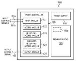
- FIG. 1 illustrates a block diagram of a semiconductor memory system 100 as provided by one embodiment of the disclosure.
- the semiconductor memory system 100 includes a plurality of memory blocks 105 , a power supply 110 coupled to the plurality of memory blocks 105 , and a power controller 120 coupled to the power supply 110 .
- the semiconductor memory system 100 also includes first and second input memory mode signals 101 a , 101 b and an output status signal 103 .
- the power controller 120 includes an input module 121 , an access module 122 , a retain-till-access module 123 , an expanded retain-till-access module 124 and an output module 125 .
- the plurality of memory blocks 105 employ static random access memory (SRAM) cells, in the illustrated embodiment.
- the power supply provides each memory block with positive and negative supply voltages.
- the positive and negative supply voltages are scalable in voltage value as directed by the power controller 120 . This scalability allows each of the memory blocks to range between a fully powered supply voltage that is needed for memory access and a retention supply voltage employed to retain data storage while reducing active leakage current in the plurality of memory blocks 105 .
- the input module 121 receives the first and second input memory mode signals 101 a , 101 b , which determine an operating mode for the memory blocks 105 .
- the input module 121 then provides mutually exclusive access, retain-till-access and expanded retain-till-access control signals for the power controller 120 .
- the access module 122 is controlled by the access control signal and provides an active state of the memory blocks 105 that allows memory access, when enabled by the access control signal. In this operating mode, all of the memory blocks 105 are fully powered allowing minimum access and cycle times for memory reading and writing.
- the retain-till-access module 123 is controlled by the retain-till-access control signal and, when enabled, cycles a memory block 105 a between the active state and a low leakage data retention state that is employed for all of the memory blocks 105 .
- a memory block 105 a In this operating mode, only the memory block 105 a is allowed to be fully powered to provide minimum access and cycle times for memory reading and writing.
- the low leakage data retention state provides a minimum powered leakage for all of the memory blocks 105 .
- the memory block 105 a is a representative portion of the memory blocks 105 wherein it corresponds to a memory block controlled by a group of 32 word lines, in the illustrated embodiment. Of course, any grouping of word lines may define a memory block as deemed appropriate to a particular memory application.
- the expanded retain-till-access module 124 is controlled by the expanded retain-till-access control signal.
- This operating mode extends the active state of all of the memory blocks 105 for a specified period of time before returning all of them to the low leakage data retention state.
- the specified period of time restarts after each memory access that occurs during the extended active state.
- the specified period of time may correspond to a selected number of clock cycles employing a control counter. Alternatively, the specified period of time may be determined independent of the number of clock cycles. In either case, the specified period of time may be programmable.
- the output module 125 provides an output status signal that corresponds to extending the active state. This indicates that the memory blocks 105 are still in the active state that allows minimum access and cycle times for memory reading and writing.
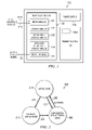
- FIG. 2 illustrates a diagram of memory power states 200 as provided by one embodiment of the disclosure.
- the memory power states 200 include a low leakage data retention state 205 , an active state 210 and an extended active state 215 . These states may be determined by a power controller such as the power controller 120 for a memory such as the plurality of memory blocks 105 of FIG. 1 .
- the low leakage data retention state 205 is applied to the entire memory when at least a portion of the memory is not residing in another state. In the low leakage data retention state 205 , the supply voltage across the memory is reduced to provide the smallest powered or active leakage current for the memory.
- the active state 210 corresponds to the largest leakage current of the memory.
- a cycle of operating states for the entire memory is different than one employed when only a portion of the memory is accessed.
- a cycle path 206 , 211 , 216 is employed for the entire memory. Transitioning from the low leakage data retention state 205 to the active state 210 for the entire memory typically produces an access latency period of at least one clock cycle. This allows time for the entire memory to become fully active from its having been in a retention mode or “sleep mode”. After this latency period, the entire memory may be accessed at minimum access and cycle times for reading or writing. At the completion of a memory access, the entire memory transitions to the extended active state 215 .
- the entire memory may still be accessed at minimum access and cycle times, without latency.
- the extended active state 215 continues until either another memory access occurs within a pre-selected, specified period of time, or the time period expires without memory access.
- the time period expires without memory access, the entire memory returns to the low leakage data retention state 205 , thereby completing a memory cycle.
- a cycle path 206 , 207 is employed when only a portion of the memory is activated for reading or writing. Transitioning the portion of the memory from the low leakage data retention state 205 to the active state 210 typically does not produce an access latency period large enough to prohibit the memory portion from being accessed during the same clock cycle. This occurs since the capacitances associated with the memory portion selected are typically small enough to allow recovery to full power quickly. The memory portion is returned to the low leakage data retention state 205 after each memory access. This allows the entire memory or a portion of the memory to be activated for another memory access.
- FIG. 3 illustrates a flow diagram of a method of operating a power controller 300 carried out according to the principles of the present disclosure.
- the method 300 is for use with a memory in a powered state and starts in a step 305 .
- a first decisional step 310 it is determined if an access mode of the memory has been selected by an enabling access control signal. If the access mode has been selected, a fully active state is provided that allows access for reading from and writing to all of the memory, in a step 315 .
- a second decisional step 320 determines if the memory is still in the powered state. If the memory is still in the powered state and the access mode of the first decisional step 310 is still enabled, the method 300 returns to the step 315 for the next memory access.
- the method 300 continues to the third decisional step 325 wherein it is determined if a retain-till-access mode of the memory has been selected by an enabling retain-till-access control signal. If the retain-till-access mode has been selected, the fully active state is provided for a portion of the memory thereby allowing the memory portion to be accessed, in a step 330 . Correspondingly, the remainder of the memory resides in a low leakage data retention state, which provides a minimum active leakage current for the remainder of the memory. In the fully active state, the portion of the memory is accessed only once before it cycles to the low leakage data retention state. This places all of the memory in the low leakage data retention state.
- the second decisional step 320 determines if the memory is still in the powered state. If the memory is still powered, and the first and third decisional steps 310 , 325 determine that the access mode is not enabled and the retain-till-access mode is still enabled, the method 300 returns to the step 330 for the next access of the portion of the memory.
- step 335 is an expanded retain-till-access mode.
- An expanded retain-till-access control signal enables the expanded retain-till-access mode, wherein all of the memory is initially placed in the low leakage data retention state thereby providing the minimum active leakage current for the memory. The fully active state is provided for all of the memory when it is accessed.
- the fully active state of the memory is extended for a specified period of time before the memory is returned to the low leakage data retention state.
- extending the fully active state restarts after each memory access during the specified period of time.
- the specified period of time may correspond to a preset timer or to a selected number of clock cycles that may be measured by a control counter. In either of these cases, the specified period of time may be programmable.
- a fully active state status signal is provided during the specified period of time to indicate that memory access is immediately available.
- the second decisional step 320 again determines if the memory is still in the powered state. If the memory is still powered, and the first and third decisional steps 310 , 325 determine that the access and the retain-till-access modes are not enabled, the method 300 returns to the step 335 for the next memory access. In this manner, the method 300 continues to select an appropriate mode as long as the memory remains in the powered state. If the second decisional step 320 determines that the memory is not in the powered state, the method 300 ends in a step 340 .
Landscapes
- Engineering & Computer Science (AREA)
- Power Engineering (AREA)
- Static Random-Access Memory (AREA)
Abstract
Description
- This application claims the benefit of U.S. Provisional Application No. 60/862,705 entitled “Leakage Reduction Modes for Semiconductor Memories” to Michael P. Clinton, et al., filed on Oct. 24, 2006, which is incorporated herein by reference in its entirety.
- The present disclosure is directed, in general, to memory systems and, more specifically, to a power controller, a method of operating a power controller and a semiconductor memory system employing the controller or the method.
- Portable electronic devices are increasingly more feature-rich, often requiring wireless communications and multimedia processing. These devices are also trending toward smaller physical size and increased computing power. CMOS circuits can play a dominant role in such devices, which are often integrated to the point of having a complete system on a chip (SoC). Even though these devices are smaller in size, power requirements typically have not diminished due to the demand for increased functionality. Additionally, applications require memories that can offer low leakage currents while still providing fast access and cycle times. Although current devices are providing acceptable performance, further improvements would prove beneficial in the art.
- Embodiments of the present disclosure provide a power controller, a method of operating a power controller and a semiconductor memory system. In one embodiment, the power controller is for use with a memory and includes an access module configured to provide an active state of the memory to allow memory access. The power controller also includes a retain-till-access module configured to cycle a portion of the memory between the active state and a low leakage data retention state of the memory. The power controller further includes an expanded retain-till-access module configured to extend the active state of the memory for a specified period of time before returning the memory to the low leakage data retention state.
- In another aspect, the present disclosure provides a method of operating a power controller for use with a memory. The method includes providing an active state of the memory that allows memory access and cycling a portion of the memory between the active state and a low leakage data retention state of the memory. The method also includes extending the active state of the memory for a specified period of time before returning the memory to the low leakage data retention state.
- The present disclosure also provides, in yet another aspect, a semiconductor memory system. The semiconductor memory system includes a plurality of memory blocks, a power supply coupled to the plurality of memory blocks and a power controller coupled to the power supply. The power controller has an input module that receives first and second memory mode signals and provides mutually exclusive access, retain-till-access and expanded retain-till-access control signals. The power controller also has an access module, coupled to the access output control signal, which provides an active state of the memory to allow memory access. The power controller additionally has a retain-till-access module, coupled to the retain-till-access control signal, which cycles a portion of the memory between the active state and a low leakage data retention state of the memory. The power controller further has an expanded retain-till-access module, coupled to the expanded retain-till-access control signal, which extends the active state of the memory for a specified period of time before returning the memory to the low leakage data retention state. The power controller still further has an output module that provides an output status signal corresponding to extending the active state.
- The foregoing has outlined preferred and alternative features of the present disclosure so that those skilled in the art may better understand the detailed description of the disclosure that follows. Additional features of the disclosure will be described hereinafter that form the subject of the claims of the disclosure. Those skilled in the art will appreciate that they can readily use the disclosed conception and specific embodiment as a basis for designing or modifying other structures for carrying out the same purposes of the present disclosure.
- For a more complete understanding of the present disclosure, reference is now made to the following descriptions taken in conjunction with the accompanying drawings, in which:
-
FIG. 1 illustrates a block diagram of a semiconductor memory system as provided by one embodiment of the disclosure; -
FIG. 2 illustrates a diagram of memory power states as provided by one embodiment of the disclosure; and -
FIG. 3 illustrates a flow diagram of a method of operating a power controller carried out according to the principles of the present disclosure. - In systems, including SoC designs, there are often many memories that are used in varied ways. Some require fast access and cycle time and do not need low leakage current. Others may need a low leakage current and can suffer slightly lower access and cycle times that are required to get the low leakage current. Still other memories need good leakage current reduction with the fastest possible access and cycle time. Embodiments of the present disclosure provide solutions that address these various memory requirements.
-
FIG. 1 illustrates a block diagram of asemiconductor memory system 100 as provided by one embodiment of the disclosure. Thesemiconductor memory system 100 includes a plurality ofmemory blocks 105, apower supply 110 coupled to the plurality ofmemory blocks 105, and apower controller 120 coupled to thepower supply 110. Thesemiconductor memory system 100 also includes first and second inputmemory mode signals output status signal 103. Thepower controller 120 includes aninput module 121, anaccess module 122, a retain-till-access module 123, an expanded retain-till-access module 124 and anoutput module 125. - The plurality of
memory blocks 105 employ static random access memory (SRAM) cells, in the illustrated embodiment. The power supply provides each memory block with positive and negative supply voltages. The positive and negative supply voltages are scalable in voltage value as directed by thepower controller 120. This scalability allows each of the memory blocks to range between a fully powered supply voltage that is needed for memory access and a retention supply voltage employed to retain data storage while reducing active leakage current in the plurality ofmemory blocks 105. - The
input module 121 receives the first and second inputmemory mode signals memory blocks 105. Theinput module 121 then provides mutually exclusive access, retain-till-access and expanded retain-till-access control signals for thepower controller 120. Theaccess module 122 is controlled by the access control signal and provides an active state of thememory blocks 105 that allows memory access, when enabled by the access control signal. In this operating mode, all of thememory blocks 105 are fully powered allowing minimum access and cycle times for memory reading and writing. - The retain-till-
access module 123 is controlled by the retain-till-access control signal and, when enabled, cycles amemory block 105 a between the active state and a low leakage data retention state that is employed for all of thememory blocks 105. In this operating mode, only thememory block 105 a is allowed to be fully powered to provide minimum access and cycle times for memory reading and writing. The low leakage data retention state provides a minimum powered leakage for all of thememory blocks 105. Thememory block 105 a is a representative portion of thememory blocks 105 wherein it corresponds to a memory block controlled by a group of 32 word lines, in the illustrated embodiment. Of course, any grouping of word lines may define a memory block as deemed appropriate to a particular memory application. - The expanded retain-till-
access module 124 is controlled by the expanded retain-till-access control signal. This operating mode extends the active state of all of thememory blocks 105 for a specified period of time before returning all of them to the low leakage data retention state. In one embodiment, the specified period of time restarts after each memory access that occurs during the extended active state. The specified period of time may correspond to a selected number of clock cycles employing a control counter. Alternatively, the specified period of time may be determined independent of the number of clock cycles. In either case, the specified period of time may be programmable. Theoutput module 125 provides an output status signal that corresponds to extending the active state. This indicates that thememory blocks 105 are still in the active state that allows minimum access and cycle times for memory reading and writing. -
FIG. 2 illustrates a diagram of memory power states 200 as provided by one embodiment of the disclosure. The memory power states 200 include a low leakagedata retention state 205, anactive state 210 and an extendedactive state 215. These states may be determined by a power controller such as thepower controller 120 for a memory such as the plurality of memory blocks 105 ofFIG. 1 . The low leakagedata retention state 205 is applied to the entire memory when at least a portion of the memory is not residing in another state. In the low leakagedata retention state 205, the supply voltage across the memory is reduced to provide the smallest powered or active leakage current for the memory. Alternatively, theactive state 210 corresponds to the largest leakage current of the memory. - A cycle of operating states for the entire memory is different than one employed when only a portion of the memory is accessed. A
cycle path data retention state 205 to theactive state 210 for the entire memory typically produces an access latency period of at least one clock cycle. This allows time for the entire memory to become fully active from its having been in a retention mode or “sleep mode”. After this latency period, the entire memory may be accessed at minimum access and cycle times for reading or writing. At the completion of a memory access, the entire memory transitions to the extendedactive state 215. - In the extended
active state 215, the entire memory may still be accessed at minimum access and cycle times, without latency. The extendedactive state 215 continues until either another memory access occurs within a pre-selected, specified period of time, or the time period expires without memory access. When the time period expires without memory access, the entire memory returns to the low leakagedata retention state 205, thereby completing a memory cycle. - A
cycle path data retention state 205 to theactive state 210 typically does not produce an access latency period large enough to prohibit the memory portion from being accessed during the same clock cycle. This occurs since the capacitances associated with the memory portion selected are typically small enough to allow recovery to full power quickly. The memory portion is returned to the low leakagedata retention state 205 after each memory access. This allows the entire memory or a portion of the memory to be activated for another memory access. -
FIG. 3 illustrates a flow diagram of a method of operating apower controller 300 carried out according to the principles of the present disclosure. Themethod 300 is for use with a memory in a powered state and starts in astep 305. Then, in a firstdecisional step 310, it is determined if an access mode of the memory has been selected by an enabling access control signal. If the access mode has been selected, a fully active state is provided that allows access for reading from and writing to all of the memory, in astep 315. After each memory access in thestep 315, a seconddecisional step 320 determines if the memory is still in the powered state. If the memory is still in the powered state and the access mode of the firstdecisional step 310 is still enabled, themethod 300 returns to thestep 315 for the next memory access. - If the first
decisional step 310 determines that the access mode is not enabled, themethod 300 continues to the thirddecisional step 325 wherein it is determined if a retain-till-access mode of the memory has been selected by an enabling retain-till-access control signal. If the retain-till-access mode has been selected, the fully active state is provided for a portion of the memory thereby allowing the memory portion to be accessed, in astep 330. Correspondingly, the remainder of the memory resides in a low leakage data retention state, which provides a minimum active leakage current for the remainder of the memory. In the fully active state, the portion of the memory is accessed only once before it cycles to the low leakage data retention state. This places all of the memory in the low leakage data retention state. - As before, the second
decisional step 320 determines if the memory is still in the powered state. If the memory is still powered, and the first and thirddecisional steps method 300 returns to thestep 330 for the next access of the portion of the memory. - If the first and third
decisional steps method 300 continues to astep 335, which is an expanded retain-till-access mode. An expanded retain-till-access control signal enables the expanded retain-till-access mode, wherein all of the memory is initially placed in the low leakage data retention state thereby providing the minimum active leakage current for the memory. The fully active state is provided for all of the memory when it is accessed. - In this mode, the fully active state of the memory is extended for a specified period of time before the memory is returned to the low leakage data retention state. In one embodiment, extending the fully active state restarts after each memory access during the specified period of time. Additionally, the specified period of time may correspond to a preset timer or to a selected number of clock cycles that may be measured by a control counter. In either of these cases, the specified period of time may be programmable. A fully active state status signal is provided during the specified period of time to indicate that memory access is immediately available.
- After the memory is returned to the low leakage data retention state, the second
decisional step 320 again determines if the memory is still in the powered state. If the memory is still powered, and the first and thirddecisional steps method 300 returns to thestep 335 for the next memory access. In this manner, themethod 300 continues to select an appropriate mode as long as the memory remains in the powered state. If the seconddecisional step 320 determines that the memory is not in the powered state, themethod 300 ends in astep 340. - While the method disclosed herein has been described and shown with reference to particular steps performed in a particular order, it will be understood that these steps may be combined, subdivided, or reordered to form an equivalent method without departing from the teachings of the present disclosure. Accordingly, unless specifically indicated herein, the order or the grouping of the steps is not a limitation of the present disclosure.
- Those skilled in the art to which the disclosure relates will appreciate that other and further additions, deletions, substitutions and modifications may be made to the described example embodiments without departing from the disclosure.
Claims (20)
Priority Applications (1)
| Application Number | Priority Date | Filing Date | Title |
|---|---|---|---|
| US11/876,600 US8266464B2 (en) | 2006-10-24 | 2007-10-22 | Power controller, a method of operating the power controller and a semiconductor memory system employing the same |
Applications Claiming Priority (2)
| Application Number | Priority Date | Filing Date | Title |
|---|---|---|---|
| US86270506P | 2006-10-24 | 2006-10-24 | |
| US11/876,600 US8266464B2 (en) | 2006-10-24 | 2007-10-22 | Power controller, a method of operating the power controller and a semiconductor memory system employing the same |
Publications (2)
| Publication Number | Publication Date |
|---|---|
| US20080098244A1 true US20080098244A1 (en) | 2008-04-24 |
| US8266464B2 US8266464B2 (en) | 2012-09-11 |
Family
ID=39319466
Family Applications (1)
| Application Number | Title | Priority Date | Filing Date |
|---|---|---|---|
| US11/876,600 Active 2029-10-06 US8266464B2 (en) | 2006-10-24 | 2007-10-22 | Power controller, a method of operating the power controller and a semiconductor memory system employing the same |
Country Status (1)
| Country | Link |
|---|---|
| US (1) | US8266464B2 (en) |
Cited By (5)
| Publication number | Priority date | Publication date | Assignee | Title |
|---|---|---|---|---|
| US20090172449A1 (en) * | 2007-12-26 | 2009-07-02 | Ming Zhang | System-driven techniques to reduce memory operating voltage |
| US20100250980A1 (en) * | 2009-03-30 | 2010-09-30 | Mediatek Inc. | Methods for reducing power consumption and devices using the same |
| US8766707B1 (en) | 2013-03-15 | 2014-07-01 | Seagate Technology Llc | Integrated always on power island for low power mode operation |
| US9335809B2 (en) | 2013-03-15 | 2016-05-10 | Seagate Technology Llc | Volatile memory storing system data during low power mode operation and monitoring the voltage supplied to the memory during low power mode |
| US9411394B2 (en) | 2013-03-15 | 2016-08-09 | Seagate Technology Llc | PHY based wake up from low power mode operation |
Citations (11)
| Publication number | Priority date | Publication date | Assignee | Title |
|---|---|---|---|---|
| US5524248A (en) * | 1993-07-06 | 1996-06-04 | Dell Usa, L.P. | Random access memory power management system |
| US5615162A (en) * | 1995-01-04 | 1997-03-25 | Texas Instruments Incorporated | Selective power to memory |
| US5699309A (en) * | 1996-05-13 | 1997-12-16 | Motorola, Inc. | Method and apparatus for providing user selectable low power and high performance memory access modes |
| US5835435A (en) * | 1997-12-02 | 1998-11-10 | Intel Corporation | Method and apparatus for dynamically placing portions of a memory in a reduced power consumtion state |
| US5898235A (en) * | 1996-12-31 | 1999-04-27 | Stmicroelectronics, Inc. | Integrated circuit with power dissipation control |
| US6118719A (en) * | 1998-05-20 | 2000-09-12 | International Business Machines Corporation | Self-initiated self-refresh mode for memory modules |
| US20010018726A1 (en) * | 1996-05-13 | 2001-08-30 | Mitsuo Tabo | Memory refreshing system |
| US20050018528A1 (en) * | 2003-07-23 | 2005-01-27 | Frank Hellwig | Memory arrangement for processing data, and method |
| US20050094473A1 (en) * | 1993-01-07 | 2005-05-05 | Takeshi Sakata | Semiconductor integrated circuits with power reduction mechanism |
| US20050135175A1 (en) * | 2003-12-22 | 2005-06-23 | Texas Instruments Incorporated | SRAM with temperature-dependent voltage control in sleep mode |
| US20060259791A1 (en) * | 2005-05-10 | 2006-11-16 | Dockser Kenneth A | Idle-element prediction circuitry and anti-thrashing logic |
-
2007
- 2007-10-22 US US11/876,600 patent/US8266464B2/en active Active
Patent Citations (11)
| Publication number | Priority date | Publication date | Assignee | Title |
|---|---|---|---|---|
| US20050094473A1 (en) * | 1993-01-07 | 2005-05-05 | Takeshi Sakata | Semiconductor integrated circuits with power reduction mechanism |
| US5524248A (en) * | 1993-07-06 | 1996-06-04 | Dell Usa, L.P. | Random access memory power management system |
| US5615162A (en) * | 1995-01-04 | 1997-03-25 | Texas Instruments Incorporated | Selective power to memory |
| US5699309A (en) * | 1996-05-13 | 1997-12-16 | Motorola, Inc. | Method and apparatus for providing user selectable low power and high performance memory access modes |
| US20010018726A1 (en) * | 1996-05-13 | 2001-08-30 | Mitsuo Tabo | Memory refreshing system |
| US5898235A (en) * | 1996-12-31 | 1999-04-27 | Stmicroelectronics, Inc. | Integrated circuit with power dissipation control |
| US5835435A (en) * | 1997-12-02 | 1998-11-10 | Intel Corporation | Method and apparatus for dynamically placing portions of a memory in a reduced power consumtion state |
| US6118719A (en) * | 1998-05-20 | 2000-09-12 | International Business Machines Corporation | Self-initiated self-refresh mode for memory modules |
| US20050018528A1 (en) * | 2003-07-23 | 2005-01-27 | Frank Hellwig | Memory arrangement for processing data, and method |
| US20050135175A1 (en) * | 2003-12-22 | 2005-06-23 | Texas Instruments Incorporated | SRAM with temperature-dependent voltage control in sleep mode |
| US20060259791A1 (en) * | 2005-05-10 | 2006-11-16 | Dockser Kenneth A | Idle-element prediction circuitry and anti-thrashing logic |
Cited By (8)
| Publication number | Priority date | Publication date | Assignee | Title |
|---|---|---|---|---|
| US20090172449A1 (en) * | 2007-12-26 | 2009-07-02 | Ming Zhang | System-driven techniques to reduce memory operating voltage |
| US8589706B2 (en) * | 2007-12-26 | 2013-11-19 | Intel Corporation | Data inversion based approaches for reducing memory power consumption |
| US9720484B2 (en) | 2007-12-26 | 2017-08-01 | Intel Corporation | Apparatus and method to reduce memory power consumption by inverting data |
| US20100250980A1 (en) * | 2009-03-30 | 2010-09-30 | Mediatek Inc. | Methods for reducing power consumption and devices using the same |
| US8127167B2 (en) * | 2009-03-30 | 2012-02-28 | Mediatek Inc. | Methods for reducing power consumption and devices using the same |
| US8766707B1 (en) | 2013-03-15 | 2014-07-01 | Seagate Technology Llc | Integrated always on power island for low power mode operation |
| US9335809B2 (en) | 2013-03-15 | 2016-05-10 | Seagate Technology Llc | Volatile memory storing system data during low power mode operation and monitoring the voltage supplied to the memory during low power mode |
| US9411394B2 (en) | 2013-03-15 | 2016-08-09 | Seagate Technology Llc | PHY based wake up from low power mode operation |
Also Published As
| Publication number | Publication date |
|---|---|
| US8266464B2 (en) | 2012-09-11 |
Similar Documents
| Publication | Publication Date | Title |
|---|---|---|
| CN1811986B (en) | Semiconductor device, semiconductor memory device and method for applying memory cell power voltage | |
| US11488645B2 (en) | Methods for reading data from a storage buffer including delaying activation of a column select | |
| KR100437610B1 (en) | A low power semiconductor memory device with normal mode and partial array self refresh mode | |
| CN101465151B (en) | Memory system and control method for memory | |
| US9189052B2 (en) | Voltage regulation for data retention in a volatile memory | |
| US7523373B2 (en) | Minimum memory operating voltage technique | |
| US20140149773A1 (en) | Latch circuit and data processing system | |
| JP2009543267A (en) | Integrated circuit having memory for reading / writing operation at low voltage | |
| KR20150107891A (en) | Write driver for write assistance in memory device | |
| US8266464B2 (en) | Power controller, a method of operating the power controller and a semiconductor memory system employing the same | |
| US11264060B2 (en) | Voltage regulation system for memory bit cells | |
| JP2007122437A (en) | Semiconductor integrated circuit device | |
| DE102005011424B4 (en) | Clock stop detector | |
| KR20100087362A (en) | Systems and methods for low power, high yield memory | |
| US20030084235A1 (en) | Synchronous DRAM controller and control method for the same | |
| US9360922B2 (en) | Data processing system, microcontroller and semiconductor device | |
| JP5591621B2 (en) | Semiconductor device and control method thereof | |
| US9348770B1 (en) | Non-volatile semiconductor memory device with temporary data retention cells and control method thereof | |
| US7869244B2 (en) | Digital memory with controllable input/output terminals | |
| JP2003022670A (en) | Semiconductor integrated circuit | |
| KR100702124B1 (en) | Internal voltage supply circuit | |
| JP2017085256A (en) | Electronic circuit and control method and device of electronic circuit | |
| JP2003228982A5 (en) | ||
| US20010017810A1 (en) | Semiconductor memory device | |
| KR100745072B1 (en) | Internal voltage discharge circuit |
Legal Events
| Date | Code | Title | Description |
|---|---|---|---|
| AS | Assignment |
Owner name: TEXAS INSTRUMENTS INC., TEXAS Free format text: ASSIGNMENT OF ASSIGNORS INTEREST;ASSIGNORS:CLINTON, MICHAEL P.;HERAGU, KEERTHINARAYAN P.;KO, UMING U.;REEL/FRAME:020001/0197;SIGNING DATES FROM 20071019 TO 20071022 Owner name: TEXAS INSTRUMENTS INC., TEXAS Free format text: ASSIGNMENT OF ASSIGNORS INTEREST;ASSIGNORS:CLINTON, MICHAEL P.;HERAGU, KEERTHINARAYAN P.;KO, UMING U.;SIGNING DATES FROM 20071019 TO 20071022;REEL/FRAME:020001/0197 |
|
| STCF | Information on status: patent grant |
Free format text: PATENTED CASE |
|
| FPAY | Fee payment |
Year of fee payment: 4 |
|
| MAFP | Maintenance fee payment |
Free format text: PAYMENT OF MAINTENANCE FEE, 8TH YEAR, LARGE ENTITY (ORIGINAL EVENT CODE: M1552); ENTITY STATUS OF PATENT OWNER: LARGE ENTITY Year of fee payment: 8 |
|
| MAFP | Maintenance fee payment |
Free format text: PAYMENT OF MAINTENANCE FEE, 12TH YEAR, LARGE ENTITY (ORIGINAL EVENT CODE: M1553); ENTITY STATUS OF PATENT OWNER: LARGE ENTITY Year of fee payment: 12 |