US20080098166A1 - Data storage device and data controlling method - Google Patents
Data storage device and data controlling method Download PDFInfo
- Publication number
- US20080098166A1 US20080098166A1 US11/974,771 US97477107A US2008098166A1 US 20080098166 A1 US20080098166 A1 US 20080098166A1 US 97477107 A US97477107 A US 97477107A US 2008098166 A1 US2008098166 A1 US 2008098166A1
- Authority
- US
- United States
- Prior art keywords
- logical
- space
- logical space
- storage device
- data storage
- Prior art date
- Legal status (The legal status is an assumption and is not a legal conclusion. Google has not performed a legal analysis and makes no representation as to the accuracy of the status listed.)
- Abandoned
Links
Images


Classifications
-
- G—PHYSICS
- G06—COMPUTING OR CALCULATING; COUNTING
- G06F—ELECTRIC DIGITAL DATA PROCESSING
- G06F12/00—Accessing, addressing or allocating within memory systems or architectures
- G06F12/02—Addressing or allocation; Relocation
- G06F12/0223—User address space allocation, e.g. contiguous or non contiguous base addressing
- G06F12/023—Free address space management
- G06F12/0238—Memory management in non-volatile memory, e.g. resistive RAM or ferroelectric memory
- G06F12/0246—Memory management in non-volatile memory, e.g. resistive RAM or ferroelectric memory in block erasable memory, e.g. flash memory
-
- G—PHYSICS
- G06—COMPUTING OR CALCULATING; COUNTING
- G06F—ELECTRIC DIGITAL DATA PROCESSING
- G06F3/00—Input arrangements for transferring data to be processed into a form capable of being handled by the computer; Output arrangements for transferring data from processing unit to output unit, e.g. interface arrangements
- G06F3/06—Digital input from, or digital output to, record carriers, e.g. RAID, emulated record carriers or networked record carriers
- G06F3/0601—Interfaces specially adapted for storage systems
- G06F3/0602—Interfaces specially adapted for storage systems specifically adapted to achieve a particular effect
- G06F3/0614—Improving the reliability of storage systems
- G06F3/0619—Improving the reliability of storage systems in relation to data integrity, e.g. data losses, bit errors
-
- G—PHYSICS
- G06—COMPUTING OR CALCULATING; COUNTING
- G06F—ELECTRIC DIGITAL DATA PROCESSING
- G06F3/00—Input arrangements for transferring data to be processed into a form capable of being handled by the computer; Output arrangements for transferring data from processing unit to output unit, e.g. interface arrangements
- G06F3/06—Digital input from, or digital output to, record carriers, e.g. RAID, emulated record carriers or networked record carriers
- G06F3/0601—Interfaces specially adapted for storage systems
- G06F3/0628—Interfaces specially adapted for storage systems making use of a particular technique
- G06F3/0638—Organizing or formatting or addressing of data
- G06F3/064—Management of blocks
-
- G—PHYSICS
- G06—COMPUTING OR CALCULATING; COUNTING
- G06F—ELECTRIC DIGITAL DATA PROCESSING
- G06F3/00—Input arrangements for transferring data to be processed into a form capable of being handled by the computer; Output arrangements for transferring data from processing unit to output unit, e.g. interface arrangements
- G06F3/06—Digital input from, or digital output to, record carriers, e.g. RAID, emulated record carriers or networked record carriers
- G06F3/0601—Interfaces specially adapted for storage systems
- G06F3/0628—Interfaces specially adapted for storage systems making use of a particular technique
- G06F3/0638—Organizing or formatting or addressing of data
- G06F3/0644—Management of space entities, e.g. partitions, extents, pools
-
- G—PHYSICS
- G06—COMPUTING OR CALCULATING; COUNTING
- G06F—ELECTRIC DIGITAL DATA PROCESSING
- G06F3/00—Input arrangements for transferring data to be processed into a form capable of being handled by the computer; Output arrangements for transferring data from processing unit to output unit, e.g. interface arrangements
- G06F3/06—Digital input from, or digital output to, record carriers, e.g. RAID, emulated record carriers or networked record carriers
- G06F3/0601—Interfaces specially adapted for storage systems
- G06F3/0668—Interfaces specially adapted for storage systems adopting a particular infrastructure
- G06F3/0671—In-line storage system
- G06F3/0673—Single storage device
- G06F3/0679—Non-volatile semiconductor memory device, e.g. flash memory, one time programmable memory [OTP]
Definitions
- the present invention contains subject matter related to Japanese Patent Application JP 2006-285297 filed in the Japan Patent Office on Oct. 19, 2006, the entire contents of which being incorporated herein by reference.
- the present invention relates to a data storage device and a data controlling method that can divide a logical space within a memory.
- Patent Document 1 Japanese Patent No. 3699890 describes a nonvolatile semiconductor storage device that can simultaneously perform erasure, writing, and reading in partition units.
- This Patent Document 1 includes a description to the effect that a partition used in the nonvolatile semiconductor storage device includes a plurality of memory blocks, and that the number of memory blocks included in one partition can be changed by external command control.
- partitions can be set only in a memory initialized to become a completely free space, and partition configuration cannot be changed in a state in which data is written in the memory.
- the present invention is proposed in view of such an actual situation, and it is desirable to provide a data storage device and a data controlling method that can divide a logical space into a plurality of logical spaces according to a request of a user even in a memory area in which data is written.
- a data storage device detachably connected to a host device, the data storage device including: a memory having a logical space composed of at least one logical unit; a logical space managing table for managing the logical space; and controlling means for controlling a managing operation of the logical space managing table, and when the host device makes a request to divide the logical space, searching the logical space for unused logical blocks, dividing a logical space composed of the unused logical blocks from the logical space, and performing control to manage a plurality of the obtained logical spaces as different logical units, respectively.
- a data controlling method for use by a data storage device including a memory having a logical space composed of at least one logical unit and being detachably connected to a host device, the data controlling method including: controlling a managing operation of a logical space managing table for managing the logical space, and when the host device makes a request to divide the logical space, searching the logical space for unused logical blocks, dividing a logical space composed of the unused logical blocks from the logical space, and performing control to manage a plurality of the obtained logical spaces as different logical units, respectively.
- FIG. 1 is a diagram showing a configuration of a data communication system according to an embodiment to which the present invention is applied;
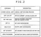
- FIG. 2 is a diagram showing an example of commands issued by an application executed by a host device
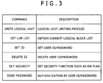
- FIG. 3 is a diagram showing an example of commands issued by an application executed by the host device
- FIG. 4 is a diagram showing a physical space and a logical space possessed by a flash memory
- FIG. 5 is a diagram showing an example of security functions set to logical units
- FIG. 6 is a flowchart of assistance in explaining an example of a process of dividing a logical space
- FIG. 7 is a diagram showing an initial state of the memory
- FIGS. 8A and 8B are diagrams representing an example of the logical space dividing process
- FIGS. 9A and 9B are diagrams representing an example of the logical space dividing process
- FIG. 10 is a flowchart of assistance in explaining an example of a process of uniting logical spaces
- FIGS. 11A and 11B are diagrams representing an example of the logical space uniting process.
- FIGS. 12A and 12B are diagrams representing an example of the logical space uniting process.
- a nonvolatile semiconductor storage device is applied as a data storage device according to the embodiment of the present invention.
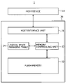
- FIG. 1 is a diagram showing a configuration of a data communication system 1 according to an embodiment to which the present invention is applied.
- the data communication system 1 includes a host device 10 and a nonvolatile semiconductor storage device 20 detachably connectable to the host device 10 .
- the host device 10 can be for example a CE (Consumer Electronics) device such as a digital camera or the like, or a personal computer.
- the host device 10 has an internal configuration of an ordinary information processing device in which a CPU (Central Processing Unit), a ROM (Read Only Memory), and a RAM (Random Access Memory) are connected to an internal bus.
- a CPU Central Processing Unit
- ROM Read Only Memory
- RAM Random Access Memory
- the host device 10 transmits and receives data and commands to and from the nonvolatile semiconductor storage device 20 using SCSI (Small Computer System Interface).
- SCSI Small Computer System Interface
- the nonvolatile semiconductor storage device 20 includes a host interface unit 21 , a flash memory 22 , and a memory controlling unit 23 for controlling the flash memory 22 .
- the nonvolatile semiconductor storage device 20 includes a CPU, a ROM, a RAM and the like (not shown).
- the CPU reads a program stored in the ROM, expands the program into the RAM, and executes the program, thereby controlling data processing in general.
- the RAM manages a logical block list including information indicating current use states (a used state, an unused state or the like) of logical blocks, and has a logical space managing table 24 for associating logical block addresses and physical block addresses with each other, and managing the logical block addresses and the physical block addresses.
- An application program for dividing a logical space or uniting logical spaces in the flash memory 22 is written to the ROM provided in the nonvolatile semiconductor storage device 20 .
- This application program is expanded and executed in the RAM of the host device 10 .
- this application may be installed onto the host device 10 by a user and then executed.
- the application issues a command for the dividing process, a command for the uniting process, and a command for setting a security function for a logical unit as shown in FIG. 2 and FIG. 3 , for example.
- a command for the dividing process a command for the uniting process
- a command for setting a security function for a logical unit as shown in FIG. 2 and FIG. 3 , for example.
- the host interface unit 21 transmits and receives data to and from the host device 10 .
- the host interface unit 21 receives a command issued by the application being executed by the host device 10 , and notifies the description of the command to the memory controlling unit 23 .
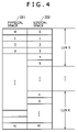
- the flash memory 22 has a physical space 221 composed of N+1 physical blocks and a logical space 222 composed of N+1 logical blocks.
- the physical blocks forming the physical space 221 are a physical space in which data is stored.
- the logical blocks forming the logical space 222 are a space in which data to be processed is written when the host device 10 performs a process of for example overwriting or reading the data.
- a logical block address ( 0 , 1 , . . . , M) as an index value in a virtual memory of the nonvolatile semiconductor storage device 20 is given to each logical block.
- a logical space composed of a predetermined number of logical blocks is set as one logical unit.
- Logical unit numbers (LUNs) such as LUN 0 , LUN 1 , and LUNK in order are given to respective logical units.
- LUNs Logical unit numbers
- a logical space composed of a logical block 0 , a logical block 1 , . . . , and a logical block 5 shown in FIG. 4 is managed as LUN 0 .
- the memory controlling unit 23 searches the logical space 222 for logical blocks in which data is not written, that is, unused logical blocks on the basis of a predetermined command issued by the application, divides a logical space composed of the unused logical blocks from the original logical space, and manages the plurality of logical spaces obtained by this dividing process as different logical units (LUN 0 , LUN 1 , . . . , and LUNK) within the logical space managing table 24 .
- logical units LUN 0 , LUN 1 , . . . , and LUNK
- the logical space managing table 24 manages, as a logical space list, information on the number of logical blocks in which data is written, that is, used logical blocks, the number of unused logical blocks, correspondences between logical block addresses ( 0 , 1 , . . . , and M) and LUNs (LUN 0 , LUN 1 , . . . , and LUNK), the number of logical units, logical unit numbers (LUN), a used space of the logical space, a free space of the logical space, and the like.
- the logical space managing table 24 associates the logical block addresses given to the logical blocks 222 as objects of data processing with the physical block addresses given to the physical blocks 221 , and manages the logical block addresses and the physical block addresses.
- the memory controlling unit 23 controls the managing operation of such a logical space managing table 24 . For example, when the memory controlling unit 23 receives a command (Get LUN List) requesting obtainment of a logical block list within the flash memory 22 from the host device 10 via the host interface unit 21 , the memory controlling unit 23 transmits information of the logical block list to the host device 10 .
- a command Get LUN List
- the memory controlling unit 23 transmits information of the logical block list to the host device 10 .
- the memory controlling unit 23 When the memory controlling unit 23 receives a command requesting reading, writing, erasing or the like of data stored in the flash memory 22 from the host device 10 via the host interface unit 21 , the memory controlling unit 23 refers to the logical space managing table 24 , converts the logical block address of a logical block in which the data to be read, written, or erased, for example, is stored into a physical block address, and identifies a physical block that has the physical block address and in which the data is stored. The memory controlling unit 23 then performs the reading, writing, erasing or the like of the data.
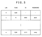
- the memory controlling unit 23 can set security functions such as a flag, an ID, and a password to each logical unit indicated by LUN 0 , . . . , LUNn.
- security functions such as a flag, an ID, and a password to each logical unit indicated by LUN 0 , . . . , LUNn.
- a flag R indicates that only a reading process is allowed.
- a flag W indicates that only a writing process is allowed.
- a flag R/W indicates that reading and writing are both allowed.
- An ID and a password play a role of lock release, which is necessary when each logical unit is accessed.
- a user can access the logical unit LUN 0 without inputting an ID or a password, and perform both a reading process and a writing process on the logical unit LUN 0 .
- the user can access the logical unit LUN 1 by inputting an ID 0001 and a password abcd, and perform only a reading process on the logical unit LUN 1 .
- the user can access the logical unit LUNn by inputting an ID 1111 and a password vwxy, and perform both a reading process and a writing process on the logical unit LUNn.
- FIG. 6 is a flowchart of assistance in explaining an example of the process of dividing a logical space in the nonvolatile semiconductor storage device 20 .
- step S 1 the host device 10 starts an application.
- the application issues a command for the dividing process, a command for setting security functions to a logical unit, and the like.
- the host device 10 transmits a command (Get LUN List) to the nonvolatile semiconductor storage device 20 .
- the memory controlling unit 23 receives the command (Get LUN List) via the host interface unit 21 , the memory controlling unit 23 transmits, to the host device 10 , information on the number of used logical blocks, the number of unused logical blocks, correspondences between logical block addresses ( 0 , 1 , and M) and LUNs (LUN 0 , LUN 1 , .
- LUN logical unit numbers
- step S 2 when the application requests obtainment of a divisible maximum size of a logical space, the host device 10 transmits a command (Get Max Size) to the nonvolatile semiconductor storage device 20 . Receiving the command (Get Max Size) via the host interface unit 21 , the memory controlling unit 23 calculates the divisible maximum size of a logical space by searching the logical space 222 for unused logical blocks. The memory controlling unit 23 then transmits the divisible maximum size of the logical space 222 to the host device 10 . In step S 2 , the memory controlling unit 23 searches even a logical unit having logical blocks in which data is written for a free space composed of unused logical blocks.
- step S 3 when the user specifies a desired size referring to the divisible maximum size on the application, the host device 10 transmits the size specified by the user to the nonvolatile semiconductor storage device 20 .
- step S 4 the host device 10 transmits a command (Divide Logical Unit) for dividing a logical space of the size specified by the user on the application to the nonvolatile semiconductor storage device 20 .
- the memory controlling unit 23 receives the command (Divide Logical Unit) via the host interface unit 21 , the memory controlling unit 23 obtains a free space of the size specified by the user from the logical space 222 possessed by the flash memory 22 . Then, the memory controlling unit 23 divides the obtained logical space composed of unused logical blocks from the logical space 222 .
- the memory controlling unit 23 manages the plurality of logical spaces obtained by this dividing process as new separate logical units, respectively.
- step S 5 the memory controlling unit 23 formats each of the logical units obtained by the dividing process in step S 4 .
- step S 6 the memory controlling unit 23 determines whether to set security functions to the newly set logical units (LUN 0 , LUN 1 , . . . ) according to contents input by the user.
- step S 7 the memory controlling unit 23 sets security functions such as a flag, an ID, and a password to the newly set logical units.
- the memory controlling unit 23 compares the divisible maximum size of the logical space 222 with the size specified by the user in advance, and the divisible maximum size of the logical space 222 is equal to or larger than the size specified by the user, a logical space of the size specified by the user which logical space is composed of unused logical blocks is obtained by the above-described dividing process, and when the divisible maximum size of the logical space 222 is smaller than the size specified by the user, the above-described dividing process may be prevented from being performed.
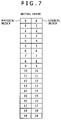
- FIG. 7 is a diagram showing an example of an initial state of the memory having a physical space formed by unused physical blocks (a physical block 0 , . . . , and a physical block 19 ) and a logical space formed by unused logical blocks (a logical block 0 , . . . , and a logical block 19 ).
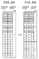
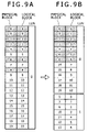
- FIGS. 8A , 8 B, 9 A, and 9 B are diagrams showing examples of dividing the logical space in a state in which some of the physical blocks and the logical blocks shown in FIG. 7 are used.
- FIG. 8A when a logical space composed of the logical block 13 , . . . , and the logical block 19 corresponding to the physical block 13 , . . . , and the physical block 19 , respectively, is divided from the original logical space, as shown in FIG. 8B , the logical blocks corresponding to the physical block 13 , . . . , and the physical block 19 obtained by the dividing process are given logical block numbers 0 , . . . , and 6 in order, and a logical space formed of the newly obtained logical blocks 0 , . . . , and 6 is given a logical unit number LUN 1 and managed.
- the logical block 5 corresponding to the physical block 5 when the logical block 5 corresponding to the physical block 5 , the logical block 7 corresponding to the physical block 7 , and the logical block 9 , . . . , and the logical block 13 corresponding to the physical block 9 , . . . , and the physical block 13 , respectively, are grouped together and divided from the original logical space
- the logical blocks corresponding to the physical block 5 , . . . , and the physical block 13 obtained by the dividing process are given logical block numbers 0 , . . . , and 6 in order, and a logical space formed of the newly obtained logical blocks 0 , . . . , and 6 is given a logical unit number LUN 1 and managed.
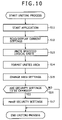
- FIG. 10 is a flowchart of assistance in explaining an example of the process of uniting logical spaces in the nonvolatile semiconductor storage device 20 .
- step S 11 the host device 10 starts an application.
- the application issues commands shown in FIG. 3 , for example.
- step S 12 after the host device 10 transmits a command (Get LUN List) to the nonvolatile semiconductor storage device 20 , the memory controlling unit 23 transmits, to the host device 10 , information on the number of logical units existing in the flash memory 22 , logical unit numbers (LUN), a used space of the logical units, a free space of the logical units, and the like.
- the host device 10 presents these pieces of information obtained from the nonvolatile semiconductor storage device 20 to the user on the application.
- step S 13 after the user specifies logical units to be united referring to the information presented on the application, the host device 10 transmits a command (Unite Logical Unit) requesting a process of uniting the logical units to be united to the nonvolatile semiconductor storage device 20 .
- the memory controlling unit 23 performs the process of uniting the logical units to be united.
- step S 14 the memory controlling unit 23 formats a logical space obtained by the uniting process.
- the memory controlling unit 23 manages each logical space as a logical unit (LUN 0 , LUN 1 , . . . ).
- step S 15 information on the logical unit obtained by the uniting process is updated, and various function settings for the logical unit are changed.
- step S 16 the memory controlling unit 23 determines whether to set security functions to the newly set logical unit (LUN 0 , LUN 1 , . . . ) according to contents input by the user.
- step S 16 the process proceeds to step S 17 , where the memory controlling unit 23 sets security functions such as a flag, an ID, and a password to the newly set logical unit.
- step S 16 the series of uniting processes is ended.
- FIGS. 11A , 11 B, 12 A, and 12 B are diagrams showing examples of uniting logical spaces in a state in which some of the physical blocks and the logical blocks shown in FIG. 7 are used.
- the logical space is divided into logical spaces LUN 0 , LUN 1 , and LUN 2
- data stored in the physical block 6 and the physical block 8 in the logical space LUN 1 as shown in FIG. 11A may be erased, and thereafter the logical spaces LUN 0 and LUN 1 may be united as shown in FIG. 11B so that a new logical space composed of the logical spaces LUN 0 and LUN 1 is obtained.
- the logical spaces LUN 1 and LUN 2 may be united as shown in FIG. 12B to obtain a logical space composed of new logical spaces LUN 0 and LUN 1 .
- the logical space within the flash memory 22 is logically divided by the control of the memory controlling unit 23 provided in the nonvolatile semiconductor storage device 20 . Therefore the host device 10 does not perform a special process, and a risk of data being destroyed accidentally by the user can be avoided.
- the nonvolatile semiconductor storage device 20 can set security functions such as a flag, an ID, and a password to each logical space.
- security functions such as a flag, an ID, and a password
- the nonvolatile semiconductor storage device 20 divides or unites logical spaces within the flash memory 22 according to a request of the user. Therefore one memory area can be used differently for various purposes.
Landscapes
- Engineering & Computer Science (AREA)
- Theoretical Computer Science (AREA)
- Physics & Mathematics (AREA)
- General Engineering & Computer Science (AREA)
- General Physics & Mathematics (AREA)
- Human Computer Interaction (AREA)
- Computer Security & Cryptography (AREA)
- Information Retrieval, Db Structures And Fs Structures Therefor (AREA)
- Storage Device Security (AREA)
- Memory System (AREA)
Abstract
A data storage device detachably connected to a host device, the data storage device including: a memory having a logical space composed of at least one logical unit; a logical space managing table for managing the logical space; and a controlling section configured to control a managing operation of the logical space managing table, and when the host device makes a request to divide the logical space, searching the logical space for unused logical blocks, dividing a logical space composed of the unused logical blocks from the logical space, and performing control to manage a plurality of the obtained logical spaces as different logical units, respectively.
Description
- The present invention contains subject matter related to Japanese Patent Application JP 2006-285297 filed in the Japan Patent Office on Oct. 19, 2006, the entire contents of which being incorporated herein by reference.
- 1. Field of the Invention
- The present invention relates to a data storage device and a data controlling method that can divide a logical space within a memory.
- 2. Description of the Related Art
- There is an existing technology for dividing a logical space into a predetermined number of areas in a storage device or the like to use the memory areas for different purposes.
- For example, the following Patent Document 1 (Japanese Patent No. 3699890) describes a nonvolatile semiconductor storage device that can simultaneously perform erasure, writing, and reading in partition units. This
Patent Document 1 includes a description to the effect that a partition used in the nonvolatile semiconductor storage device includes a plurality of memory blocks, and that the number of memory blocks included in one partition can be changed by external command control. - However, in general, when a memory is divided by partitions, partitions can be set only in a memory initialized to become a completely free space, and partition configuration cannot be changed in a state in which data is written in the memory.
- The present invention is proposed in view of such an actual situation, and it is desirable to provide a data storage device and a data controlling method that can divide a logical space into a plurality of logical spaces according to a request of a user even in a memory area in which data is written.
- According to an embodiment of the present invention, there is provided a data storage device detachably connected to a host device, the data storage device including: a memory having a logical space composed of at least one logical unit; a logical space managing table for managing the logical space; and controlling means for controlling a managing operation of the logical space managing table, and when the host device makes a request to divide the logical space, searching the logical space for unused logical blocks, dividing a logical space composed of the unused logical blocks from the logical space, and performing control to manage a plurality of the obtained logical spaces as different logical units, respectively.
- According to an embodiment of the present invention, there is provided a data controlling method for use by a data storage device, the data storage device including a memory having a logical space composed of at least one logical unit and being detachably connected to a host device, the data controlling method including: controlling a managing operation of a logical space managing table for managing the logical space, and when the host device makes a request to divide the logical space, searching the logical space for unused logical blocks, dividing a logical space composed of the unused logical blocks from the logical space, and performing control to manage a plurality of the obtained logical spaces as different logical units, respectively.
- According to the present invention, even a logical unit in which data is written is searched for a free space corresponding to a memory space requested by a command. It is thereby possible to make effective use of a memory area according to purposes of the user.
-
FIG. 1 is a diagram showing a configuration of a data communication system according to an embodiment to which the present invention is applied; -
FIG. 2 is a diagram showing an example of commands issued by an application executed by a host device; -
FIG. 3 is a diagram showing an example of commands issued by an application executed by the host device; -
FIG. 4 is a diagram showing a physical space and a logical space possessed by a flash memory; -
FIG. 5 is a diagram showing an example of security functions set to logical units; -
FIG. 6 is a flowchart of assistance in explaining an example of a process of dividing a logical space; -
FIG. 7 is a diagram showing an initial state of the memory; -
FIGS. 8A and 8B are diagrams representing an example of the logical space dividing process; -
FIGS. 9A and 9B are diagrams representing an example of the logical space dividing process; -
FIG. 10 is a flowchart of assistance in explaining an example of a process of uniting logical spaces; -
FIGS. 11A and 11B are diagrams representing an example of the logical space uniting process; and -
FIGS. 12A and 12B are diagrams representing an example of the logical space uniting process. - A concrete embodiment to which the present invention is applied will hereinafter be described in detail with reference to the drawings. In the present embodiment, a nonvolatile semiconductor storage device is applied as a data storage device according to the embodiment of the present invention.
-
FIG. 1 is a diagram showing a configuration of adata communication system 1 according to an embodiment to which the present invention is applied. Thedata communication system 1 includes ahost device 10 and a nonvolatilesemiconductor storage device 20 detachably connectable to thehost device 10. - The
host device 10 can be for example a CE (Consumer Electronics) device such as a digital camera or the like, or a personal computer. Thehost device 10 has an internal configuration of an ordinary information processing device in which a CPU (Central Processing Unit), a ROM (Read Only Memory), and a RAM (Random Access Memory) are connected to an internal bus. - The
host device 10 transmits and receives data and commands to and from the nonvolatilesemiconductor storage device 20 using SCSI (Small Computer System Interface). - The nonvolatile
semiconductor storage device 20 includes ahost interface unit 21, aflash memory 22, and amemory controlling unit 23 for controlling theflash memory 22. In addition, the nonvolatilesemiconductor storage device 20 includes a CPU, a ROM, a RAM and the like (not shown). The CPU reads a program stored in the ROM, expands the program into the RAM, and executes the program, thereby controlling data processing in general. In addition, the RAM manages a logical block list including information indicating current use states (a used state, an unused state or the like) of logical blocks, and has a logical space managing table 24 for associating logical block addresses and physical block addresses with each other, and managing the logical block addresses and the physical block addresses. - An application program for dividing a logical space or uniting logical spaces in the
flash memory 22 is written to the ROM provided in the nonvolatilesemiconductor storage device 20. This application program is expanded and executed in the RAM of thehost device 10. Incidentally, this application may be installed onto thehost device 10 by a user and then executed. - In order to perform a process of dividing a logical space or uniting logical spaces in the
flash memory 22 provided in the nonvolatilesemiconductor storage device 20 on the basis of a request by the user, the application issues a command for the dividing process, a command for the uniting process, and a command for setting a security function for a logical unit as shown inFIG. 2 andFIG. 3 , for example. Incidentally, details of the process of dividing a logical space or the process of uniting logical spaces on the basis of these commands will be described later. - The
host interface unit 21 transmits and receives data to and from thehost device 10. In addition, thehost interface unit 21 receives a command issued by the application being executed by thehost device 10, and notifies the description of the command to thememory controlling unit 23. - As shown in
FIG. 4 , theflash memory 22 has aphysical space 221 composed of N+1 physical blocks and alogical space 222 composed of N+1 logical blocks. - The physical blocks forming the
physical space 221 are a physical space in which data is stored. A physical block address n (n=0, 1, . . . , N) is given to each physical block. - The logical blocks forming the
logical space 222 are a space in which data to be processed is written when thehost device 10 performs a process of for example overwriting or reading the data. A logical block address (0, 1, . . . , M) as an index value in a virtual memory of the nonvolatilesemiconductor storage device 20 is given to each logical block. In thelogical space 222, a logical space composed of a predetermined number of logical blocks is set as one logical unit. Logical unit numbers (LUNs) such as LUN0, LUN1, and LUNK in order are given to respective logical units. For example, a logical space composed of alogical block 0, alogical block 1, . . . , and alogical block 5 shown inFIG. 4 is managed as LUN0. - The
memory controlling unit 23 searches thelogical space 222 for logical blocks in which data is not written, that is, unused logical blocks on the basis of a predetermined command issued by the application, divides a logical space composed of the unused logical blocks from the original logical space, and manages the plurality of logical spaces obtained by this dividing process as different logical units (LUN0, LUN1, . . . , and LUNK) within the logical space managing table 24. - The logical space managing table 24 manages, as a logical space list, information on the number of logical blocks in which data is written, that is, used logical blocks, the number of unused logical blocks, correspondences between logical block addresses (0, 1, . . . , and M) and LUNs (LUN0, LUN1, . . . , and LUNK), the number of logical units, logical unit numbers (LUN), a used space of the logical space, a free space of the logical space, and the like. In addition, the logical space managing table 24 associates the logical block addresses given to the
logical blocks 222 as objects of data processing with the physical block addresses given to thephysical blocks 221, and manages the logical block addresses and the physical block addresses. - The
memory controlling unit 23 controls the managing operation of such a logical space managing table 24. For example, when thememory controlling unit 23 receives a command (Get LUN List) requesting obtainment of a logical block list within theflash memory 22 from thehost device 10 via thehost interface unit 21, thememory controlling unit 23 transmits information of the logical block list to thehost device 10. When thememory controlling unit 23 receives a command requesting reading, writing, erasing or the like of data stored in theflash memory 22 from thehost device 10 via thehost interface unit 21, thememory controlling unit 23 refers to the logical space managing table 24, converts the logical block address of a logical block in which the data to be read, written, or erased, for example, is stored into a physical block address, and identifies a physical block that has the physical block address and in which the data is stored. Thememory controlling unit 23 then performs the reading, writing, erasing or the like of the data. - In addition, as shown in
FIG. 5 , for example, thememory controlling unit 23 can set security functions such as a flag, an ID, and a password to each logical unit indicated by LUN0, . . . , LUNn. In this case, a flag R indicates that only a reading process is allowed. A flag W indicates that only a writing process is allowed. A flag R/W indicates that reading and writing are both allowed. An ID and a password play a role of lock release, which is necessary when each logical unit is accessed. - For example, a user can access the logical unit LUN0 without inputting an ID or a password, and perform both a reading process and a writing process on the logical unit LUN0. The user can access the logical unit LUN1 by inputting an
ID 0001 and a password abcd, and perform only a reading process on the logical unit LUN1. The user can access the logical unit LUNn by inputting anID 1111 and a password vwxy, and perform both a reading process and a writing process on the logical unit LUNn. - Description will next be made of the process of dividing a
logical space 222 and the process of unitinglogical spaces 222 in the nonvolatilesemiconductor storage device 20. -
FIG. 6 is a flowchart of assistance in explaining an example of the process of dividing a logical space in the nonvolatilesemiconductor storage device 20. - When the dividing process is initiated, in step S1, the
host device 10 starts an application. As shown inFIG. 2 ; for example, the application issues a command for the dividing process, a command for setting security functions to a logical unit, and the like. When the application requests obtainment of a logical space list, thehost device 10 transmits a command (Get LUN List) to the nonvolatilesemiconductor storage device 20. Receiving the command (Get LUN List) via thehost interface unit 21, thememory controlling unit 23 transmits, to thehost device 10, information on the number of used logical blocks, the number of unused logical blocks, correspondences between logical block addresses (0, 1, and M) and LUNs (LUN0, LUN1, . . . , and LUNK), the number of logical units, logical unit numbers (LUN), a used space of the logical space, a free space of the logical space, and the like entered in the logical space list stored in the logical space managing table 24. - In step S2, when the application requests obtainment of a divisible maximum size of a logical space, the
host device 10 transmits a command (Get Max Size) to the nonvolatilesemiconductor storage device 20. Receiving the command (Get Max Size) via thehost interface unit 21, thememory controlling unit 23 calculates the divisible maximum size of a logical space by searching thelogical space 222 for unused logical blocks. Thememory controlling unit 23 then transmits the divisible maximum size of thelogical space 222 to thehost device 10. In step S2, thememory controlling unit 23 searches even a logical unit having logical blocks in which data is written for a free space composed of unused logical blocks. - In step S3, when the user specifies a desired size referring to the divisible maximum size on the application, the
host device 10 transmits the size specified by the user to the nonvolatilesemiconductor storage device 20. - In step S4, the
host device 10 transmits a command (Divide Logical Unit) for dividing a logical space of the size specified by the user on the application to the nonvolatilesemiconductor storage device 20. Receiving the command (Divide Logical Unit) via thehost interface unit 21, thememory controlling unit 23 obtains a free space of the size specified by the user from thelogical space 222 possessed by theflash memory 22. Then, thememory controlling unit 23 divides the obtained logical space composed of unused logical blocks from thelogical space 222. Thememory controlling unit 23 manages the plurality of logical spaces obtained by this dividing process as new separate logical units, respectively. - In step S5, the
memory controlling unit 23 formats each of the logical units obtained by the dividing process in step S4. - In step S6, the
memory controlling unit 23 determines whether to set security functions to the newly set logical units (LUN0, LUN1, . . . ) according to contents input by the user. When it is determined in step S6 that security functions are to be set, the process proceeds to step S7, where thememory controlling unit 23 sets security functions such as a flag, an ID, and a password to the newly set logical units. When it is determined in step S6 that security functions are not to be set, on the other hand, the series of dividing processes is ended. - Incidentally, in the present embodiment, when the
host device 10 transmits a command requesting a size specified by the user in advance to the nonvolatilesemiconductor storage device 20, thememory controlling unit 23 compares the divisible maximum size of thelogical space 222 with the size specified by the user in advance, and the divisible maximum size of thelogical space 222 is equal to or larger than the size specified by the user, a logical space of the size specified by the user which logical space is composed of unused logical blocks is obtained by the above-described dividing process, and when the divisible maximum size of thelogical space 222 is smaller than the size specified by the user, the above-described dividing process may be prevented from being performed. -
FIG. 7 is a diagram showing an example of an initial state of the memory having a physical space formed by unused physical blocks (aphysical block 0, . . . , and a physical block 19) and a logical space formed by unused logical blocks (alogical block 0, . . . , and a logical block 19). -
FIGS. 8A , 8B, 9A, and 9B are diagrams showing examples of dividing the logical space in a state in which some of the physical blocks and the logical blocks shown inFIG. 7 are used. For example, as shown inFIG. 8A , when a logical space composed of thelogical block 13, . . . , and thelogical block 19 corresponding to thephysical block 13, . . . , and thephysical block 19, respectively, is divided from the original logical space, as shown inFIG. 8B , the logical blocks corresponding to thephysical block 13, . . . , and thephysical block 19 obtained by the dividing process are givenlogical block numbers 0, . . . , and 6 in order, and a logical space formed of the newly obtainedlogical blocks 0, . . . , and 6 is given a logical unit number LUN1 and managed. - For example, as shown in
FIG. 9A , when thelogical block 5 corresponding to thephysical block 5, thelogical block 7 corresponding to thephysical block 7, and thelogical block 9, . . . , and thelogical block 13 corresponding to thephysical block 9, . . . , and thephysical block 13, respectively, are grouped together and divided from the original logical space, as shown inFIG. 9B , the logical blocks corresponding to thephysical block 5, . . . , and thephysical block 13 obtained by the dividing process are givenlogical block numbers 0, . . . , and 6 in order, and a logical space formed of the newly obtainedlogical blocks 0, . . . , and 6 is given a logical unit number LUN1 and managed. -
FIG. 10 is a flowchart of assistance in explaining an example of the process of uniting logical spaces in the nonvolatilesemiconductor storage device 20. - When the uniting process is initiated, in step S11, the
host device 10 starts an application. The application issues commands shown inFIG. 3 , for example. - In step S12, after the
host device 10 transmits a command (Get LUN List) to the nonvolatilesemiconductor storage device 20, thememory controlling unit 23 transmits, to thehost device 10, information on the number of logical units existing in theflash memory 22, logical unit numbers (LUN), a used space of the logical units, a free space of the logical units, and the like. Thehost device 10 presents these pieces of information obtained from the nonvolatilesemiconductor storage device 20 to the user on the application. - In step S13, after the user specifies logical units to be united referring to the information presented on the application, the
host device 10 transmits a command (Unite Logical Unit) requesting a process of uniting the logical units to be united to the nonvolatilesemiconductor storage device 20. Thememory controlling unit 23 performs the process of uniting the logical units to be united. - In step S14, the
memory controlling unit 23 formats a logical space obtained by the uniting process. Thememory controlling unit 23 manages each logical space as a logical unit (LUN0, LUN1, . . . ). - In step S15, information on the logical unit obtained by the uniting process is updated, and various function settings for the logical unit are changed.
- In step S16, the
memory controlling unit 23 determines whether to set security functions to the newly set logical unit (LUN0, LUN1, . . . ) according to contents input by the user. When it is determined in step S16 that security functions are to be set, the process proceeds to step S17, where thememory controlling unit 23 sets security functions such as a flag, an ID, and a password to the newly set logical unit. When it is determined in step S16 that security functions are not to be set, on the other hand, the series of uniting processes is ended. -
FIGS. 11A , 11B, 12A, and 12B are diagrams showing examples of uniting logical spaces in a state in which some of the physical blocks and the logical blocks shown inFIG. 7 are used. For example, when the logical space is divided into logical spaces LUN0, LUN1, and LUN2, according to a command indicating a request of the user, data stored in thephysical block 6 and thephysical block 8 in the logical space LUN1 as shown inFIG. 11A may be erased, and thereafter the logical spaces LUN0 and LUN1 may be united as shown inFIG. 11B so that a new logical space composed of the logical spaces LUN0 and LUN1 is obtained. In addition, according to a command indicating a request of the user, without erasing data stored in thephysical block 6 and thephysical block 8 in the logical space LUN1 as shown inFIG. 12A , the logical spaces LUN1 and LUN2 may be united as shown inFIG. 12B to obtain a logical space composed of new logical spaces LUN0 and LUN1. - Thus, in the
data communication system 1 according to one embodiment to which the present invention is applied, the logical space within theflash memory 22 is logically divided by the control of thememory controlling unit 23 provided in the nonvolatilesemiconductor storage device 20. Therefore thehost device 10 does not perform a special process, and a risk of data being destroyed accidentally by the user can be avoided. - In addition, in the
data communication system 1, the nonvolatilesemiconductor storage device 20 can set security functions such as a flag, an ID, and a password to each logical space. Thus, a high level of security can be maintained even when one nonvolatile semiconductor storage device is used by a plurality of users. - Further, in the
data communication system 1, the nonvolatilesemiconductor storage device 20 divides or unites logical spaces within theflash memory 22 according to a request of the user. Therefore one memory area can be used differently for various purposes. - It is to be noted that the present invention is not limited to only the above-described embodiments, and that various changes can of course be made without departing from the spirit of the present invention.
- It should be understood by those skilled in the art that various modifications, combinations, sub-combinations and alterations may occur depending on design requirements and other factors insofar as they are within the scope of the appended claims or the equivalents thereof.
Claims (8)
1. A data storage device detachably connected to a host device, said data storage device comprising:
a memory having a logical space composed of at least one logical unit;
a logical space managing table for managing said logical space; and
controlling means for controlling a managing operation of said logical space managing table, and when said host device makes a request to divide said logical space, searching said logical space for unused logical blocks, dividing a logical space composed of said unused logical blocks from said logical space, and performing control to manage a plurality of the obtained logical spaces as different logical units, respectively.
2. The data storage device according to claim 1 , wherein when said host device makes a request to unite said logical units, a plurality of said logical units obtained by a dividing process are united.
3. The data storage device according to claim 1 , wherein even a logical unit in which data is written is searched for said unused logical block.
4. The data storage device according to claim 1 , wherein when said controlling means receives a command requesting obtainment of a divisible maximum size of said logical space from said host device, said controlling means calculates the divisible maximum size of said logical space by searching said logical space for unused logical blocks, and presents the divisible maximum size of said logical space to said host device.
5. The data storage device according to claim 1 , wherein when said host device makes a request to divide a logical space of a size specified by a user, said controlling means compares the size specified by said user with a divisible maximum size in said logical space, said controlling means divides a logical space composed of unused said logical blocks corresponding to the size specified by said user from said logical space in a case where the divisible maximum size in said logical space is equal to or larger than the size specified by said user, and said controlling means refrains from performing a dividing process in a case where the divisible maximum size in said logical space is smaller than the size specified by said user.
6. The data storage device according to claim 1 , wherein said controlling means sets a flag allowing reading and/or writing to said logical units.
7. The data storage device according to claim 1 , wherein said controlling means sets an ID and/or a password to said logical units.
8. A data controlling method for use by a data storage device, said data storage device including a memory having a logical space composed of at least one logical unit and being detachably connected to a host device, said data controlling method comprising:
controlling a managing operation of a logical space managing table for managing said logical space, and when said host device makes a request to divide said logical space, searching said logical space for unused logical blocks, dividing a logical space composed of said unused logical blocks from said logical space, and performing control to manage a plurality of the obtained logical spaces as different logical units, respectively.
Applications Claiming Priority (2)
| Application Number | Priority Date | Filing Date | Title |
|---|---|---|---|
| JPP2006-285297 | 2006-10-19 | ||
| JP2006285297A JP2008102774A (en) | 2006-10-19 | 2006-10-19 | Data storage device and data control method |
Publications (1)
| Publication Number | Publication Date |
|---|---|
| US20080098166A1 true US20080098166A1 (en) | 2008-04-24 |
Family
ID=39319413
Family Applications (1)
| Application Number | Title | Priority Date | Filing Date |
|---|---|---|---|
| US11/974,771 Abandoned US20080098166A1 (en) | 2006-10-19 | 2007-10-16 | Data storage device and data controlling method |
Country Status (3)
| Country | Link |
|---|---|
| US (1) | US20080098166A1 (en) |
| JP (1) | JP2008102774A (en) |
| CN (1) | CN101165661A (en) |
Cited By (3)
| Publication number | Priority date | Publication date | Assignee | Title |
|---|---|---|---|---|
| US20100262765A1 (en) * | 2009-04-08 | 2010-10-14 | Samsung Electronics Co., Ltd. | Storage apparatus, computer system having the same, and methods thereof |
| US20100318760A1 (en) * | 2008-01-30 | 2010-12-16 | Hirokazu So | Memory controller, nonvolatile storage device, and nonvolatile storage system |
| US20120060203A1 (en) * | 2010-09-07 | 2012-03-08 | Susumu Aikawa | Logical unit number management device, logical unit number management method, and program therefor |
Families Citing this family (3)
| Publication number | Priority date | Publication date | Assignee | Title |
|---|---|---|---|---|
| JP2013058179A (en) * | 2011-08-18 | 2013-03-28 | Yuji Oishi | External storage device and control method thereof |
| CN106294603B (en) * | 2016-07-29 | 2019-07-23 | 北京奇虎科技有限公司 | File memory method and device |
| GB2570143B (en) * | 2018-01-12 | 2020-04-08 | Garrison Tech Ltd | Secure sharing of storage resources |
Citations (3)
| Publication number | Priority date | Publication date | Assignee | Title |
|---|---|---|---|---|
| US20050177698A1 (en) * | 2002-06-01 | 2005-08-11 | Mao-Yuan Ku | Method for partitioning memory mass storage device |
| US20070168292A1 (en) * | 2004-12-21 | 2007-07-19 | Fabrice Jogand-Coulomb | Memory system with versatile content control |
| US7343465B2 (en) * | 2005-05-27 | 2008-03-11 | Hitachi, Ltd. | Storage system |
Family Cites Families (4)
| Publication number | Priority date | Publication date | Assignee | Title |
|---|---|---|---|---|
| JP4078736B2 (en) * | 1997-11-28 | 2008-04-23 | ソニー株式会社 | Tape cassette, tape recording and / or playback device |
| JPH11167508A (en) * | 1997-12-02 | 1999-06-22 | Canon Inc | Information recording method |
| JP4279699B2 (en) * | 2003-01-31 | 2009-06-17 | パナソニック株式会社 | Semiconductor memory card, control program. |
| CN101908106B (en) * | 2004-12-21 | 2013-06-05 | 桑迪士克股份有限公司 | Memory system with versatile content control |
-
2006
- 2006-10-19 JP JP2006285297A patent/JP2008102774A/en active Pending
-
2007
- 2007-10-16 US US11/974,771 patent/US20080098166A1/en not_active Abandoned
- 2007-10-19 CN CNA2007101816040A patent/CN101165661A/en active Pending
Patent Citations (3)
| Publication number | Priority date | Publication date | Assignee | Title |
|---|---|---|---|---|
| US20050177698A1 (en) * | 2002-06-01 | 2005-08-11 | Mao-Yuan Ku | Method for partitioning memory mass storage device |
| US20070168292A1 (en) * | 2004-12-21 | 2007-07-19 | Fabrice Jogand-Coulomb | Memory system with versatile content control |
| US7343465B2 (en) * | 2005-05-27 | 2008-03-11 | Hitachi, Ltd. | Storage system |
Cited By (5)
| Publication number | Priority date | Publication date | Assignee | Title |
|---|---|---|---|---|
| US20100318760A1 (en) * | 2008-01-30 | 2010-12-16 | Hirokazu So | Memory controller, nonvolatile storage device, and nonvolatile storage system |
| US20100262765A1 (en) * | 2009-04-08 | 2010-10-14 | Samsung Electronics Co., Ltd. | Storage apparatus, computer system having the same, and methods thereof |
| US8412909B2 (en) | 2009-04-08 | 2013-04-02 | Samsung Electronics Co., Ltd. | Defining and changing spare space and user space in a storage apparatus |
| US20120060203A1 (en) * | 2010-09-07 | 2012-03-08 | Susumu Aikawa | Logical unit number management device, logical unit number management method, and program therefor |
| US8799996B2 (en) * | 2010-09-07 | 2014-08-05 | Nec Corporation | Logical unit number management device, logical unit number management method, and program therefor |
Also Published As
| Publication number | Publication date |
|---|---|
| CN101165661A (en) | 2008-04-23 |
| JP2008102774A (en) | 2008-05-01 |
Similar Documents
| Publication | Publication Date | Title |
|---|---|---|
| US11120081B2 (en) | Key-value storage device and method of operating key-value storage device | |
| JP6553566B2 (en) | Memory system and control method | |
| US20200089619A1 (en) | Data storage device and method of deleting namespace thereof | |
| KR20210108107A (en) | Memory system and operating method thereof | |
| EP2869203B1 (en) | Computer system, and arrangement of data control method | |
| US20130311704A1 (en) | Data storage device and method for flash block management | |
| US20080098166A1 (en) | Data storage device and data controlling method | |
| US20170075614A1 (en) | Memory system and host apparatus | |
| TWI710905B (en) | Data storage device and method for loading logical-to-physical mapping table | |
| US20160253257A1 (en) | Data processing system and operating method thereof | |
| JPWO2005106673A1 (en) | Nonvolatile storage device and data writing method | |
| US20130103893A1 (en) | System comprising storage device and related methods of operation | |
| US20170090794A1 (en) | Method and Apparatus for Providing a Shared Nonvolatile Memory System Using a Distributed FTL Scheme | |
| US8898414B2 (en) | Storage devices and methods of driving storage devices | |
| US10162833B2 (en) | Wireless access device and wireless access system | |
| US8954692B2 (en) | File protecting method and system, and memory controller and memory storage apparatus thereof | |
| KR102276912B1 (en) | Storage system and operating method thereof | |
| CN112988060A (en) | Key value storage device and method for operating key value storage device | |
| JP2018160189A (en) | Memory system | |
| JP2011175632A (en) | Semiconductor storage device, and method for controlling the same | |
| TW201220047A (en) | Method for performing automatic boundary alignment and related non-volatile memory device | |
| US20190065395A1 (en) | Storage device and data arrangement method | |
| KR101465460B1 (en) | Execution method for trim and data managing apparatus | |
| JP4807683B2 (en) | Data storage | |
| US11954368B2 (en) | Memory system controlling nonvolatile memory |
Legal Events
| Date | Code | Title | Description |
|---|---|---|---|
| AS | Assignment |
Owner name: SONY CORPORATION, JAPAN Free format text: ASSIGNMENT OF ASSIGNORS INTEREST;ASSIGNORS:NAKANISHI, KENICHI;NAKAJIMA, DAISUKE;OKUBO, HIDEAKI;REEL/FRAME:021227/0541 Effective date: 20070919 |
|
| STCB | Information on status: application discontinuation |
Free format text: ABANDONED -- FAILURE TO RESPOND TO AN OFFICE ACTION |