US20080098164A1 - SRAM Cache & Flash Micro-Controller with Differential Packet Interface - Google Patents
SRAM Cache & Flash Micro-Controller with Differential Packet Interface Download PDFInfo
- Publication number
- US20080098164A1 US20080098164A1 US11/876,251 US87625107A US2008098164A1 US 20080098164 A1 US20080098164 A1 US 20080098164A1 US 87625107 A US87625107 A US 87625107A US 2008098164 A1 US2008098164 A1 US 2008098164A1
- Authority
- US
- United States
- Prior art keywords
- flash
- differential
- host
- boot
- data
- Prior art date
- Legal status (The legal status is an assumption and is not a legal conclusion. Google has not performed a legal analysis and makes no representation as to the accuracy of the status listed.)
- Granted
Links
Images


Classifications
-
- G—PHYSICS
- G06—COMPUTING OR CALCULATING; COUNTING
- G06F—ELECTRIC DIGITAL DATA PROCESSING
- G06F12/00—Accessing, addressing or allocating within memory systems or architectures
- G06F12/02—Addressing or allocation; Relocation
- G06F12/08—Addressing or allocation; Relocation in hierarchically structured memory systems, e.g. virtual memory systems
- G06F12/0802—Addressing of a memory level in which the access to the desired data or data block requires associative addressing means, e.g. caches
- G06F12/0866—Addressing of a memory level in which the access to the desired data or data block requires associative addressing means, e.g. caches for peripheral storage systems, e.g. disk cache
-
- G—PHYSICS
- G06—COMPUTING OR CALCULATING; COUNTING
- G06F—ELECTRIC DIGITAL DATA PROCESSING
- G06F2212/00—Indexing scheme relating to accessing, addressing or allocation within memory systems or architectures
- G06F2212/20—Employing a main memory using a specific memory technology
- G06F2212/202—Non-volatile memory
- G06F2212/2022—Flash memory
-
- G—PHYSICS
- G06—COMPUTING OR CALCULATING; COUNTING
- G06F—ELECTRIC DIGITAL DATA PROCESSING
- G06F2212/00—Indexing scheme relating to accessing, addressing or allocation within memory systems or architectures
- G06F2212/25—Using a specific main memory architecture
- G06F2212/251—Local memory within processor subsystem
- G06F2212/2515—Local memory within processor subsystem being configurable for different purposes, e.g. as cache or non-cache memory
Definitions
- This invention relates to flash micro-controllers, and more particularly to flash microcontrollers with a cache SRAM for booting an external device over a differential interface.
- Flash memories use non-volatile memory cells such as electrically-erasable programmable read-only memory, (EEPROM), but are not randomly accessible at the byte level. Instead, whole pages or sectors of 512 bytes or more are read or written together as a single page.
- EEPROM electrically-erasable programmable read-only memory
- NAND flash memory is commonly used for data storage of blocks. Pages in the same block may have to be erased together, and limitations on writing may exist, such as only being allowed to write each page once between erases.
- Program code is often stored in randomly-accessible memory such as a ROM or a NOR flash memory. Since NOR flash memory is byte-addressable, NOR flash can store code that can be executed. Byte-addressing is needed to execute code, since branch and jump instructions may have a target that is at a random location that must be fetched next. The target may be byte-addressable. Since boot routines execute instructions one at a time, rather than a whole page at a time, randomly-accessible memory is needed for boot-code execution.
- Small portable devices such as personal digital assistants (PDA), multi-function cell phones, digital cameras, music players, etc. have a central processing unit (CPU) or microcontroller that must be booted just as a PC or host CPU must be booted. These small devices are often quite cost and size sensitive. Having a NOR flash or ROM may increase the size and cost of these portable devices.
- PDA personal digital assistants
- CPU central processing unit
- NOR flash or ROM may increase the size and cost of these portable devices.
- NAND flash memory is less expensive than NOR flash memory, and thus preferable from a cost standpoint. NAND flash memory may already be present on some devices such as cell phones or music players as the primary mass storage memory. It is thus desirable to use NAND flash memory to store boot code.
- Computers once required a complex series of steps to initialize and make them ready to run programs. Instructions for bootstrapping the computer were loaded into the computer after power-on, such as by manually toggling switches representing the 1's and 0's of bootstrap instructions on the front panel. The computer was brought from a dead state into a useful state, like lifting the computer up by its own bootstraps.
- OS operating system
- the initial instructions may reside in a read-only memory (ROM), along with a personal computer's Basic Input-Output System (BIOS).
- BIOS Basic Input-Output System
- the operating system such as Windows may be loaded from the hard disk, and when booting is complete the OS can execute user programs.
- Various system checks such as peripheral device and memory detection and sizing can be performed during booting.
- Both the flash device and the host must be booted at some point in time.
- the host is booted from its hard disk before the flash device is inserted into the host.
- the flash device is then booted when power from the host reaches the flash device.
- Cache memories are commonly used by host computers.
- a cache of the flash memory is desirable. Using this cache memory for booting both the flash-memory device and the external host is also desirable.
- flash-memory microcontroller that is bootable from boot code stored in flash memory. It is further desired to boot both the flash microcontroller and the host.
- a flash microcontroller with a differential interface to the external host that is used to transfer boot code to the external host is also desired.
- FIG. 1 is a block diagram of a flash microcontroller with a differential interface to an external host that receives host boot code from a boot-loader SRAM for dual-device booting.
- FIG. 2 shows a flash device in more detail.
- FIG. 3 shows a flash memory
- FIG. 4 shows a differential serial interface for a flash microcontroller in more detail.
- FIG. 5 shows the differential receive path in more detail.
- FIG. 6 shows the differential transmit path in more detail.
- FIGS. 7 A-B are flowcharts of read cache operations of the SRAM buffer.
- FIGS. 8 A-B are flowcharts of write cache operations of the SRAM buffer.
- FIG. 9 is a block diagram of a Secure-Digital (SD) flash microcontroller.
- SD Secure-Digital
- FIG. 10 is a diagram showing multiple flash devices ganged together in a solid-state-disk array.
- the present invention relates to an improvement in flash microcontrollers.
- the following description is presented to enable one of ordinary skill in the art to make and use the invention as provided in the context of a particular application and its requirements.
- Various modifications to the preferred embodiment will be apparent to those with skill in the art, and the general principles defined herein may be applied to other embodiments. Therefore, the present invention is not intended to be limited to the particular embodiments shown and described, but is to be accorded the widest scope consistent with the principles and novel features herein disclosed.
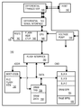
- FIG. 1 is a block diagram of a flash microcontroller with a differential interface to an external host that receives host boot code from a boot-loader SRAM for dual-device booting. Flash device 140 is plugged into host 142 and powers up when plugged in.
- Flash device 140 generates internal supply voltages from an external power supply input using voltage pump 144 .
- Central Processing Unit (CPU) 146 processes commands from host 142 which update operating registers 162 which control operation of flash memory controller 148 .
- Operating registers 162 , CPU 146 , and flash memory controller 148 may be part of microcontroller 168 .
- a high-speed differential interface is placed between host 142 and flash device 140 .
- Commands, addresses, and data are received as serial data by differential transceiver 145 , and responses and data are sent back to host 142 by differential transceiver 145 .
- Differential serial interface 143 receives a serial stream of data from differential transceiver 145 and extracts commands, data, and addresses from packets sent over the differential interface, and performs transaction handshaking or other requirements of the differential protocol. Differential serial interface 143 also generates headers, checksums, and divides data into multiple packets for transmission over the differential interface to host 142 by differential transceiver 145 .
- Flash interface 150 provides a lower-level memory interface to multi-level-cell MLC flash memory 152 , which may contain one or more flash-memory chips, and to SRAM.
- SRAM buffer 154 may contain block and page buffers of data that is stored in MLC flash memory 152 , such as boot code. SRAM buffer 154 stores both blocks and smaller pages. Pages are stored in page buffer 160 .
- Flash interface 150 generates signals for address, data, and command buses and associated control signals to the physical memory devices, both flash and SRAM.
- a SRAM cache of the data in MLC flash memory 152 is also provided by SRAM data cache 158 , with its associated tags stored in SRAM tags 156 . Requests that match SRAM tags 156 may be accessed in SRAM data cache 158 , which has a faster access time than MLC flash memory 152 .
- FIG. 2 shows a flash device in more detail.
- Microcontroller 168 receives high-level requests from a host using a bus protocol and generates lower-level memory-access commands that are sent to flash interface 150 .
- Flash interface reads, writes, and erases flash memory in MLC flash memory 152 , but can also access data more quickly using SRAM buffers 154 .
- SRAM buffers 154 is an array of SRAM that can be partitioned into a cache with SRAM tags 156 and SRAM data cache 158 .
- SRAM buffers 154 can also include buffers used to store boot code that is read from MLC flash memory 152 .
- Blocks A, B, C can store blocks of boot or operating system (OS) code read from MLC flash memory 152 .
- boot-loader state machine 172 can be activated. Boot-loader state machine 172 configures flash interface 150 by reading parameters from a flash ID and programming these flash parameters into flash parameter registers 166 for use by flash interface 150 .
- flash parameters are device-specific, and include device specifications such as the density and width of MLC flash memory 152 , the number of cycles needed for access, and other timing requirements that must be met.
- boot-loader state machine 172 configures flash interface 150
- boot-loader state machine 172 activates flash interface 150 to read the first page of the first block from MLC flash memory 152 .
- This first page contains system pointers to boot code in the flash. These pointers are flowed to locate instructions to jump to in the initial boot code, or in extended boot code. Additional boot code, control programs, and OS images are successively read from MLC flash memory 152 and loaded into SRAM buffers 154 for execution by the CPU in microcontroller 168 . Once this CPU is booted and running its OS, more boot code for the external host may be read from MLC flash memory 152 and sent to the host, so that the host can be booted.
- mappings from host (logical) addresses to flash (physical) addresses may be stored in mapping table 170 .
- Flash interface 150 uses these mappings in mapping table 170 to locate physical pages in MLC flash memory 152 that correspond to the logical addresses from host requests.
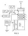
- FIG. 3 shows a flash memory.
- Flash memory 152 may include some or all of the blocks shown in FIG. 3 , and other blocks, or some of the functions may be performed by a separate flash controller. Flash memory 152 may be a separate flash chip or may be integrated with the flash microcontroller.
- Flash-memory MLC cells 110 is an array of rows and columns of multi-level cell (MLC) EEPROM transistors that can store multiple bits of data in each memory cell using different voltage levels.
- MLC cell's voltage levels are sensed by sense amplifiers 134 when a read current is drawn through a selected row of MLC cells.
- Word line drivers 128 drives one row or word line in MLC cells 110 while the other rows are disabled.
- a row portion of an address applied to address decoder 112 is further decoded by X decoder 124 to select which row to activate using word line drivers 128 .
- a column portion of the address applied to address decoder 112 is further decoded by Y decoder 132 to select a group of bit lines for data access.
- Data buffers 126 may be a limited width, such as 64 bits, while MLC cells may have a larger number of bit lines, such as 8 ⁇ 64 columns. One of the 8 columns may be selected by Y decoder 132 for connection to data buffers 126 .
- write drivers 136 During writing, external data is collected by data buffers 126 and applied to write drivers 136 .
- Write drivers 136 generate voltages or currents so that the set currents are applied to bit lines for MLC cells that are to be written with a 1, while reset currents are applied to bit lines for MLC cells to be reset to 0.
- State machines 122 can activate control logic 120 to enable and disable write drivers 136 after programming or erasure. State machines 122 can generate various internal control signals at appropriate times, such as strobes to pre-charge bit lines and latch sensed data into data buffers 126 .
- Command register 114 can receive commands that are decoded and processed by control logic 120 . External control signals such as read/write, data strobes, and byte enables may also be received in some embodiments. Command register 114 may be replaced by a command decoder in some embodiments. Power management unit 116 can power down blocks to reduce power consumption, such as when the MLC flash memory is de-selected. Since MLC cells 110 are non-volatile, data is retained when power is disconnected.
- An array-select portion of the address can be decoded by address decoders 112 to enable one of the many arrays or blocks on the MLC flash memory or chip.
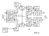
- FIG. 4 shows a differential serial interface for a flash microcontroller in more detail.
- Host serializing unit 36 connects to differential transceiver 145 ( FIG. 1 ) while receive hold register 58 and transmit hold register 68 connect to microcontroller 168 .
- Differential serial interface 143 operates between differential transceiver 145 to host 144 , and microcontroller 168 .
- Host serializing unit 36 includes receive deserializer 44 which forms parallel data from the serial data stream received from the host, and transmit serializer 48 , which converts parallel data into a serial data stream for differential transmission to the host.
- Status and control registers 46 controls and reports the status of operation of host serializing unit 36 .
- External crystal 30 provides a clock signal to clock mux 40 , which selects a clock to apply to delay line phase-locked loop (PLL) 42 .
- PLL 42 generates a clock to read FIFO 50 , which stores the deserialized data from receive deserializer 44 .
- Parallel data is also clocked out of write FIFO 60 to transmit serializer 48 by the clock from PLL 42 .
- Receive data is processed by NRZI decoder 51 to remove not-return-to-zero decoding of the differential data.
- Bit unstuffer 52 removes stuff bits that were added by the host to fill packets or frames.
- Receive shift register 56 then shifts the decoded, unstuffed data into receive hold register 58 for use by microcontroller 168 .
- Receive state control logic 54 controls operation of the receive path.
- Transmit state control logic 64 controls operation of the transmit path.
- Data from microcontroller 168 is latched into transmit hold register 68 and then shifted through transmit shift register 66 to bit stuffer 62 , which adds stuffing bits as needed to fill out packets or frames to the protocol-specified size.
- NRZI encoder 61 converts the data to not-return-to-zero encoding as differential data. The NRZI data is then stored in write FIFO 60 for later transmission as differential data.
- NRZI decoder 51 and NRZI encoder 61 can be an 8-10 bit encoder/decoder in some embodiments. Other modifications to NRZI decoder 51 and NRZI encoder 61 can be made for use with other protocols such as PCIE, USB 3.0, etc.
- FIG. 5 shows the differential receive path in more detail.
- a serial stream of data from differential transceiver 145 is amplified from a small-swing signal to a larger swing by differential detector 802 and converted to parallel data words by converter 804 .
- the clock is extracted or recovered from the data stream by clock separator 806 .
- Read-FIFO adjuster 810 adjusts the timing of data as it is stored into the read FIFO.
- Sync packet detector 812 searches for the packet's sync pattern while end of packet detector 814 searches for end-of-packet markers in the data stream.
- Frame detector 816 searches for frame markers.
- Command and data separator 818 locates commands in the data stream and separates these commands from the data.
- Data recovery unit 820 recovers the protocol data within the data stream, while checksum unit 822 generates a running checksum or cyclical-redundancy-check (CRC) of the recovered data and compares the checksum to a transmitted checksum to verify the data transmission.
- CRC cyclical-redundancy-check
- the parallel data may then be sent to microcontroller 168 for use by the flash interface.
- This parallel data may include addresses, flash commands, and data for the flash interface.
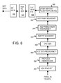
- FIG. 6 shows the differential transmit path in more detail.
- Parallel transmit data from microcontroller 168 is latched and a sync packet marker is added by sync packet unit 854 .
- Commands and data are mixed together according to the differential protocol by protocol mixer 852 .
- Data redundancy such as a CRC or checksum is added by checksum unit 850 .
- the CRC or checksum is generated by CRC generator 848 .
- Packet boundaries are added by packetizer 846 , while frame boundaries are added by frame boundary unit 842 after frames are checked and any frame redundancy or stuff bits are added by frame checker 844 .
- Dual-port write FIFO 840 buffers the data stream and adjusts the flow for stream synchronization.
- a transmit clock is mixed in with the data stream, and encoding such as NRZI decoding is added by clock mixer 836 .
- the parallel data words are converted to serial data by sterilizer 834 and the serial data is further formatted in the differential, serial format by differential converter 832 , which creates a small-voltage-swing analog signal for transmission.
- FIGS. 7 A-B are flowcharts of read cache operations of the SRAM buffer.
- the SRAM buffer can be used for blocks of boot code read by the local CPU or the external host CPU during booting. Once booting is completed, some or all of this boot code may not longer be needed.
- the SRAM buffer could then be used for caching data from the flash memory. Alternately, the size of the SRAM buffer could be large enough for both a cache and for boot-code blocks for boot code storage.
- a read request of the flash memory is received from the host.
- the host address is a logical address
- the logical block index (LBI) is extracted from the host logical address, step 402 .
- the last 6 bits of the LBI are extracted as the page index, step 404 .
- the logical sector index (LSI) which is the lower part of the logical address that does not include the LBI, selects one of the tags in the cache, step 406 , while the page index selects the row within the cache.
- the selected tag has a stored tag address that corresponds to the LBI without the page index, and this stored tag is compared to the LBI without the page index, step 408 , to determine whether an address match has been found.
- step 410 When the address matches, and a valid bit indicates that the cached data is valid, a hit occurs, step 410 . Then the requested data is read from the data portion of the cache in the SRAM buffer for that page index and selected sector (LSI), step 412 . The requested data is sent by the microcontroller to the host over the differential interface, and a ready signal is returned to the host, step 414 .
- LSI page index and selected sector
- mapping table 170 ( FIG. 2 ) is consulted with the logical address to find the physical address in the flash memory, step 422 . Any old data in the cache line is written back to flash memory, step 430 . The physical address from mapping table 170 is used to fetch data from the flash memory, step 424 . This fetched data is written into the data fields of the cache line, step 426 and is returned to the host along with the ready signal.
- the tag address can be updated with the new address using the LBI without the page index, since the page index selects the line within the cache.
- the LSI selects which sector-tag within the line to update, step 428 .
- FIGS. 8 A-B are flowcharts of write cache operations of the SRAM buffer.
- a write request of the flash memory is received from the host.
- the host address is a logical sector address
- the logical block index (LBI) is extracted from the host logical address, step 442 .
- the last 6 bits of the LBI are extracted as the page index, step 444 .
- the logical sector index (LSI) which is the lower part of the logical address that does not include the LBI, selects one of 8 tags in the cache, step 446 , while the page index selects the row within the cache.
- the selected tag has a stored tag address that corresponds to the LBI without the page index, and this stored tag is compared to the LBI without the page index, step 448 , to determine whether an address match has been found.
- step 450 the host data is written to the data portion of the cache in the SRAM buffer for that page index and selected sector (LSI), step 452 .
- the ready signal is returned to the host, step 454 .
- mapping table 170 ( FIG. 2 ) is consulted with the logical address to find the physical address in the flash memory, step 462 . Any old data in the cache line is written back to flash memory, step 470 , using this physical address from mapping table 170 .
- the host data is written into the data fields of the cache line, step 466 .
- the tag address can be updated with the new address using the LBI without the page index, since the page index selects the line within the cache.
- the LSI selects which sector-tag within the line to update, step 468 .
- FIG. 9 is a block diagram of a Secure-Digital (SD) flash microcontroller.
- SD flash microcontroller 100 can be booted from external flash memory.
- Internal bus 96 connects CPU 82 with SRAM 86 , FIFO data buffer 94 , direct-memory access (DMA) engine 88 , and flash-memory controller 90 .
- CPU 82 executes instructions read from SRAM 86 , using cache 79 to cache instructions and/or data.
- DMA direct-memory access
- DMA engine 88 can be programmed to transfer data between FIFO data buffer 94 and flash-memory controller 90 .
- CPU 82 can operate on or modify the data by reading the data over bus 96 .
- Cache 79 and external RAM can store instructions for execution by the CPU and data operated on by the CPU.
- SD transceiver 84 connects to the clock CLK and parallel data lines D 0 : 3 of SD bus 16 and contains both a clocked receiver and a transmitter.
- An interrupt to CPU 82 can be generated when a new command is detected on SD bus 16 .
- CPU 82 can then execute a routine to handle the interrupt and process the new command.
- SD operating registers 80 include the protocol registers required by the SD specification. Registers may include a data-port, write-protect, flash select, flash status, interrupt, and identifier registers. Other extension registers may also be present.
- Command decode and validator 89 detects, decodes, and validates commands received over SD bus 16 .
- Valid commands may alter bus-cycle sequencing by bus state machine 83 , and may cause response generator 87 to generate a response, such as an acknowledgement or other reply.
- Different routines can be executed by CPU 82 or different transfer lengths can be performed by DMA engine 88 in response to the byte or sector capacity detected by command decode and validator 89 .
- the transmit and receive data from SD engine 81 is stored in FIFO data buffer 94 , perhaps before or after passing through a data-port register in SD operating registers 80 .
- Commands and addresses from the SD transactions can also be stored in FIFO data buffer 94 , to be read by CPU 82 to determine what operation to perform.
- Flash-memory controller 90 may also include a flash data buffer, which may contain the commands, addresses, and data sent over flash bus 18 to one or more flash mass-storage chips. Data can be arranged to match the bus width of flash bus 18 , such as in 32 or 94-bit words. DMA engine 88 can be programmed by CPU 82 to transfer a block of data between flash bus 18 and FIFO data buffer 94 .
- Flash-specific registers in flash control registers 93 may include a data port register, interrupt, flash command and selection registers, flash-address and block-length registers, and cycle registers.
- Error-corrector 92 can read parity or error-correction code (ECC) from flash mass storage chips and perform data corrections.
- ECC error-correction code
- the parity or ECC bits for data in that is being written to flash mass storage chips can be generated by error-corrector 92 .
- Flash programming engine 97 can be a state machine that is activated on power-up reset. Flash programming engine 97 programs DMA engine 88 with the address of the boot loader code in the first page of the external flash mass-storage chip, and the first address in cache 79 or in another local RAM, or in SRAM 86 . Then flash programming engine 97 commands DMA engine 88 to transfer the boot loader from the flash mass storage chip to cache 79 or the other SRAM buffer, or to the external RAM. CPU 82 is then brought out of reset, executing the boot loader program starting from the first address in cache 79 or the SRAM buffer. The boot loader program can contain instructions to move a larger control program from the flash mass storage chip to SRAM 86 . Thus SD flash microcontroller 100 is booted without an internal ROM on internal bus 96 .
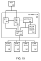
- FIG. 10 is a diagram showing multiple flash devices ganged together in a solid-state-disk array.
- Each of multiple flash devices 140 , 140 ′ contains differential transceiver 145 , microcontroller 168 , flash interface 150 , SRAM buffer 154 , flash memory 152 , etc. as shown earlier in FIGS. 1-4 .
- Host 142 is able to access a much larger amount of flash memory by ganging multiple flash devices 140 , 140 ′ together using SSD array controller 520 .
- each flash device has its own control unit to cover first-level booting as well as wear-leveling and other housekeeping work, such as bad-block management. It is more efficient for a SSD array to adopt this cluster approach as to decentralize the heavy load of microcontroller 168 described earlier.
- a differential interface is preferred in this application; however, other non-differential interfaces such as SD, MMC etc, may also be applicable in this clustering SSD-array approach.
- SSD array controller 520 is a solid-state-disk array controller that receives commands from host 142 and dispatches these commands to one of multiple flash devices 140 , 140 ′ using dispatch unit 502 .
- CPU 506 and controller 508 control operation of SSD array controller 520 , processing host commands in disk command register 504 .
- Sector buffer memory 512 temporarily stores sectors of data from host 142 that have not yet been dispatched to one of multiple flash devices 140 , 140 ′ by dispatch unit 502 .
- USB Universal-Serial Bus
- PCI Express Peripheral Component Interconnect Express
- PCI express pins include a transmit differential pair PET+, PET ⁇ , and a receive differential pair PER+, PER ⁇ of data pins.
- a multi-bus-protocol chip could have an additional personality pin to select which serial-bus interface to use, or could have programmable registers.
- ExpressCard has both the USB and the PCI Express bus, so either or both buses could be present on an ExpressCard device.
- SD, MicroSD, MMC, or microMMC interfaces can also be applied in this invention.
- other buses may be used such as Memory Stick (MS), Compact Flash (CF), IDE bus, etc.
- Additional pins can be added or substituted for the SD data pins.
- a multi-bus-protocol chip could have an additional personality pin to select which bus interface to use, or could have programmable registers.
- a Memory Stick microcontroller could be substituted, for use with a memory-stick interface, etc.
- a non-differential interface such as SD, MMC etc, serves as the link between an SSD array controller and each individual flash device. This may be more efficient for handling first-level controller booting as well as local management tasks which relieve the load of a SSD array controller.
- Flash blocks may have 4 pages, 8 pages, 64 pages, or some other number, depending on the physical flash chips and arrangement used.
- SD may be considered an extension of MMC, or a particular type of MMC, rather than a separate type of bus.
- ROM read-only memory
- ROM Read-wired gates that are tied to power or ground may also function as a read-only memory. While such ROM may be present, ROM is not required for storing boot code or booting instructions. A few bytes or more of ROM may be thus present for other purposes.
- Mode logic could sense the state of a pin only at power-on rather than sense the state of a dedicated pin.
- a certain combination or sequence of states of pins could be used to initiate a mode change, or an internal register such as a configuration register could set the mode.
- microcontroller and SD components such as the bus interface, DMA, flash-memory controller, transaction manager, and other controllers and functions can be implemented in a variety of ways. Functions can be programmed and executed by the CPU or other processor, or can be implemented in dedicated hardware, firmware, or in some combination. Many partitioning of the functions can be substituted.
- Data and commands may be routed in a variety of ways, such as through data-port registers, FIFO or other buffers, the CPU's registers and buffers, DMA registers and buffers, and flash registers and buffers. Some buffers may be bypassed or eliminated while others are used or present. Virtual or logical buffers rather than physical ones may also be used. Data may be formatted in a wide variety of ways.
- the host can transfer standard SD commands and data transactions to the SD transceiver during a transaction.
- Other transaction types or variations of these types can be defined for special purposes. These transactions may include a flash-controller-request, a flash-controller-reply, a boot-loader-request, a boot-loader-reply, a control-program-request, a control-program-reply, a flash-memory-request, and a flash-memory-reply.
- the flash-memory request/reply may further include the following request/reply pairs: flash ID, read, write, erase, copy-back, reset, page-write, cache-write and read-status.
- the host may be a personal computer (PC), a portable computing device, a digital camera, a phone, a personal digital assistant (PDA), or other electronic device.
- PC personal computer
- PDA personal digital assistant
- the partition of SRAM among various functions could change over time.
- Wider or narrower data buses and flash-memory blocks could be substituted, such as 4, 5, 8, 16, 32, 64, 128, 256-bit, or some other width data channels.
- Alternate bus architectures with nested or segmented buses could be used internal or external to the microcontroller. Two or more internal and flash buses can be used in the SD flash microcontroller to increase throughput. More complex switch fabrics can be substituted for the internal buses.
- the flash mass storage chips or blocks can be constructed from any flash technology including multi-level-logic (MLC) memory cells.
- Data striping could be used with the flash mass storage blocks in a variety of ways, as can parity and error-correction code (ECC). Data re-ordering can be adjusted depending on the data arrangement used to prevent re-ordering for overlapping memory locations.
- An SD/MMC switch could be integrated with other components or could be a stand-alone chip.
- the SD/MMC switch could also be integrated with the SD single-chip flash device. While a single-chip device has been described, separate packaged chips or die may be stacked together while sharing I/O pins, or modules may be used.
- the background of the invention section may contain background information about the problem or environment of the invention rather than describe prior art by others. Thus inclusion of material in the background section is not an admission of prior art by the Applicant.
- Tangible results generated may include reports or other machine-generated displays on display devices such as computer monitors, projection devices, audio-generating devices, and related media devices, and may include hardcopy printouts that are also machine-generated.
- Computer control of other machines is another a tangible result.
Landscapes
- Engineering & Computer Science (AREA)
- Theoretical Computer Science (AREA)
- Physics & Mathematics (AREA)
- General Engineering & Computer Science (AREA)
- General Physics & Mathematics (AREA)
- Read Only Memory (AREA)
Abstract
Description
- This application is a continuation-in-part (CIP) of the co-pending application Ser. No. 11/773,830 filed Jul. 5, 2007, for “Molding Method to Manufacture Single-Chip On-Board Device”, which is a CIP of U.S. patent application for “Single Chip Multi-Media Card/Secure Digital (MMC/SD) Controller Reading Power-on Boot Code from Integrated Flash Memory for User Storage”, U.S. application Ser. No. 11/309,594 filed Aug. 28, 2006, which is a CIP of “Single-Chip USB Controller Reading Power-on Boot Code from Integrated Flash Memory for User Storage”, U.S. application Ser. No. 10/707,277, filed Dec. 2, 2003, now U.S. Pat. No. 7,103,684.
- This is also a continuation-in-part (CIP) of the co-pending application for “Electronic Data Storage Medium with Fingerprint Verification Capability”, U.S. Ser. No. 11/624,667 filed Jan. 18, 2007, which is a divisional application of U.S. patent application Ser. No. 09/478,720, filed on Jan. 6, 2000, which has been petitioned to claim the benefit of CIP status of one of inventor's earlier U.S. patent applications for “Integrated Circuit Card with Fingerprint Verification Capability”, U.S. application Ser. No. 09/366,976, filed Aug. 4, 1999, now issued as U.S. Pat. No. 6,547,130.
- This application is related to “Flash memory device and architecture with multi level cells”, U.S. Ser. No. 10/800,228, filed Mar. 12, 2004, now U.S. Pat. No. 7,082,056, and “Flash drive/reader with serial-port controller and flash-memory controller mastering a second RAM-buffer bus parallel to a CPU bus”, U.S. Ser. No. 10/605,140, filed Sep. 10, 2003, now U.S. Pat. No. 6,874,044.
- This invention relates to flash micro-controllers, and more particularly to flash microcontrollers with a cache SRAM for booting an external device over a differential interface.
- Hard disks and other mass storage devices are being replaced or supplemented with solid-state mass storage such as flash memories. Flash memories use non-volatile memory cells such as electrically-erasable programmable read-only memory, (EEPROM), but are not randomly accessible at the byte level. Instead, whole pages or sectors of 512 bytes or more are read or written together as a single page. NAND flash memory is commonly used for data storage of blocks. Pages in the same block may have to be erased together, and limitations on writing may exist, such as only being allowed to write each page once between erases.
- Program code is often stored in randomly-accessible memory such as a ROM or a NOR flash memory. Since NOR flash memory is byte-addressable, NOR flash can store code that can be executed. Byte-addressing is needed to execute code, since branch and jump instructions may have a target that is at a random location that must be fetched next. The target may be byte-addressable. Since boot routines execute instructions one at a time, rather than a whole page at a time, randomly-accessible memory is needed for boot-code execution.
- Small portable devices such as personal digital assistants (PDA), multi-function cell phones, digital cameras, music players, etc. have a central processing unit (CPU) or microcontroller that must be booted just as a PC or host CPU must be booted. These small devices are often quite cost and size sensitive. Having a NOR flash or ROM may increase the size and cost of these portable devices.
- NAND flash memory is less expensive than NOR flash memory, and thus preferable from a cost standpoint. NAND flash memory may already be present on some devices such as cell phones or music players as the primary mass storage memory. It is thus desirable to use NAND flash memory to store boot code.
- Computers once required a complex series of steps to initialize and make them ready to run programs. Instructions for bootstrapping the computer were loaded into the computer after power-on, such as by manually toggling switches representing the 1's and 0's of bootstrap instructions on the front panel. The computer was brought from a dead state into a useful state, like lifting the computer up by its own bootstraps.
- More recently, computers still execute a complex sequence of instructions after power-on to boot the computer and load its operating system (OS). The initial instructions may reside in a read-only memory (ROM), along with a personal computer's Basic Input-Output System (BIOS). The operating system such as Windows may be loaded from the hard disk, and when booting is complete the OS can execute user programs. Various system checks such as peripheral device and memory detection and sizing can be performed during booting.
- Both the flash device and the host must be booted at some point in time. Typically, the host is booted from its hard disk before the flash device is inserted into the host. The flash device is then booted when power from the host reaches the flash device.
- Cache memories are commonly used by host computers. A cache of the flash memory is desirable. Using this cache memory for booting both the flash-memory device and the external host is also desirable.
- What is desired is a flash-memory microcontroller that is bootable from boot code stored in flash memory. It is further desired to boot both the flash microcontroller and the host. A flash microcontroller with a differential interface to the external host that is used to transfer boot code to the external host is also desired.
-
FIG. 1 is a block diagram of a flash microcontroller with a differential interface to an external host that receives host boot code from a boot-loader SRAM for dual-device booting. -
FIG. 2 shows a flash device in more detail. -
FIG. 3 shows a flash memory. -
FIG. 4 shows a differential serial interface for a flash microcontroller in more detail. -
FIG. 5 shows the differential receive path in more detail. -
FIG. 6 shows the differential transmit path in more detail. - FIGS. 7A-B are flowcharts of read cache operations of the SRAM buffer.
- FIGS. 8A-B are flowcharts of write cache operations of the SRAM buffer.
-
FIG. 9 is a block diagram of a Secure-Digital (SD) flash microcontroller. -
FIG. 10 is a diagram showing multiple flash devices ganged together in a solid-state-disk array. - The present invention relates to an improvement in flash microcontrollers. The following description is presented to enable one of ordinary skill in the art to make and use the invention as provided in the context of a particular application and its requirements. Various modifications to the preferred embodiment will be apparent to those with skill in the art, and the general principles defined herein may be applied to other embodiments. Therefore, the present invention is not intended to be limited to the particular embodiments shown and described, but is to be accorded the widest scope consistent with the principles and novel features herein disclosed.
-
FIG. 1 is a block diagram of a flash microcontroller with a differential interface to an external host that receives host boot code from a boot-loader SRAM for dual-device booting.Flash device 140 is plugged intohost 142 and powers up when plugged in. -
Flash device 140 generates internal supply voltages from an external power supply input usingvoltage pump 144. Central Processing Unit (CPU) 146 processes commands fromhost 142 which update operatingregisters 162 which control operation offlash memory controller 148. Operating registers 162,CPU 146, andflash memory controller 148 may be part ofmicrocontroller 168. - A high-speed differential interface is placed between
host 142 andflash device 140. Commands, addresses, and data are received as serial data bydifferential transceiver 145, and responses and data are sent back to host 142 bydifferential transceiver 145. - Differential
serial interface 143 receives a serial stream of data fromdifferential transceiver 145 and extracts commands, data, and addresses from packets sent over the differential interface, and performs transaction handshaking or other requirements of the differential protocol. Differentialserial interface 143 also generates headers, checksums, and divides data into multiple packets for transmission over the differential interface to host 142 bydifferential transceiver 145. -
Flash interface 150 provides a lower-level memory interface to multi-level-cellMLC flash memory 152, which may contain one or more flash-memory chips, and to SRAM.SRAM buffer 154 may contain block and page buffers of data that is stored inMLC flash memory 152, such as boot code.SRAM buffer 154 stores both blocks and smaller pages. Pages are stored inpage buffer 160. -
Flash interface 150 generates signals for address, data, and command buses and associated control signals to the physical memory devices, both flash and SRAM. A SRAM cache of the data inMLC flash memory 152 is also provided bySRAM data cache 158, with its associated tags stored in SRAM tags 156. Requests that match SRAM tags 156 may be accessed inSRAM data cache 158, which has a faster access time thanMLC flash memory 152. -
FIG. 2 shows a flash device in more detail.Microcontroller 168 receives high-level requests from a host using a bus protocol and generates lower-level memory-access commands that are sent toflash interface 150. Flash interface reads, writes, and erases flash memory inMLC flash memory 152, but can also access data more quickly using SRAM buffers 154. SRAM buffers 154 is an array of SRAM that can be partitioned into a cache withSRAM tags 156 andSRAM data cache 158. - SRAM buffers 154 can also include buffers used to store boot code that is read from
MLC flash memory 152. Blocks A, B, C can store blocks of boot or operating system (OS) code read fromMLC flash memory 152. When power-on is detected by power-on reset circuit 164, boot-loader state machine 172 can be activated. Boot-loader state machine 172 configuresflash interface 150 by reading parameters from a flash ID and programming these flash parameters into flash parameter registers 166 for use byflash interface 150. These flash parameters are device-specific, and include device specifications such as the density and width ofMLC flash memory 152, the number of cycles needed for access, and other timing requirements that must be met. Once boot-loader state machine 172 configuresflash interface 150, boot-loader state machine 172 activatesflash interface 150 to read the first page of the first block fromMLC flash memory 152. This first page contains system pointers to boot code in the flash. These pointers are flowed to locate instructions to jump to in the initial boot code, or in extended boot code. Additional boot code, control programs, and OS images are successively read fromMLC flash memory 152 and loaded intoSRAM buffers 154 for execution by the CPU inmicrocontroller 168. Once this CPU is booted and running its OS, more boot code for the external host may be read fromMLC flash memory 152 and sent to the host, so that the host can be booted. - Once the host is booted, mappings from host (logical) addresses to flash (physical) addresses may be stored in mapping table 170.
Flash interface 150 uses these mappings in mapping table 170 to locate physical pages inMLC flash memory 152 that correspond to the logical addresses from host requests. -
FIG. 3 shows a flash memory.Flash memory 152 may include some or all of the blocks shown inFIG. 3 , and other blocks, or some of the functions may be performed by a separate flash controller.Flash memory 152 may be a separate flash chip or may be integrated with the flash microcontroller. - Flash-
memory MLC cells 110 is an array of rows and columns of multi-level cell (MLC) EEPROM transistors that can store multiple bits of data in each memory cell using different voltage levels. The MLC cell's voltage levels are sensed bysense amplifiers 134 when a read current is drawn through a selected row of MLC cells.Word line drivers 128 drives one row or word line inMLC cells 110 while the other rows are disabled. A row portion of an address applied to addressdecoder 112 is further decoded byX decoder 124 to select which row to activate usingword line drivers 128. - A column portion of the address applied to address
decoder 112 is further decoded byY decoder 132 to select a group of bit lines for data access. Data buffers 126 may be a limited width, such as 64 bits, while MLC cells may have a larger number of bit lines, such as 8×64 columns. One of the 8 columns may be selected byY decoder 132 for connection to data buffers 126. - During writing, external data is collected by
data buffers 126 and applied to writedrivers 136.Write drivers 136 generate voltages or currents so that the set currents are applied to bit lines for MLC cells that are to be written with a 1, while reset currents are applied to bit lines for MLC cells to be reset to 0. -
State machines 122 can activatecontrol logic 120 to enable and disablewrite drivers 136 after programming or erasure.State machines 122 can generate various internal control signals at appropriate times, such as strobes to pre-charge bit lines and latch sensed data into data buffers 126. -
Command register 114 can receive commands that are decoded and processed bycontrol logic 120. External control signals such as read/write, data strobes, and byte enables may also be received in some embodiments.Command register 114 may be replaced by a command decoder in some embodiments.Power management unit 116 can power down blocks to reduce power consumption, such as when the MLC flash memory is de-selected. SinceMLC cells 110 are non-volatile, data is retained when power is disconnected. - There may be several arrays of
MLC cells 110 and associated logic on a large MLC flash chip. An array-select portion of the address can be decoded byaddress decoders 112 to enable one of the many arrays or blocks on the MLC flash memory or chip. -
FIG. 4 shows a differential serial interface for a flash microcontroller in more detail.Host serializing unit 36 connects to differential transceiver 145 (FIG. 1 ) while receivehold register 58 and transmithold register 68 connect tomicrocontroller 168. Differentialserial interface 143 operates betweendifferential transceiver 145 to host 144, andmicrocontroller 168. -
Host serializing unit 36 includes receivedeserializer 44 which forms parallel data from the serial data stream received from the host, and transmitserializer 48, which converts parallel data into a serial data stream for differential transmission to the host. Status and control registers 46 controls and reports the status of operation ofhost serializing unit 36. -
External crystal 30 provides a clock signal toclock mux 40, which selects a clock to apply to delay line phase-locked loop (PLL) 42.PLL 42 generates a clock to readFIFO 50, which stores the deserialized data from receivedeserializer 44. Parallel data is also clocked out ofwrite FIFO 60 to transmitserializer 48 by the clock fromPLL 42. - Receive data is processed by
NRZI decoder 51 to remove not-return-to-zero decoding of the differential data.Bit unstuffer 52 removes stuff bits that were added by the host to fill packets or frames. Receiveshift register 56 then shifts the decoded, unstuffed data into receivehold register 58 for use bymicrocontroller 168. Receivestate control logic 54 controls operation of the receive path. - Transmit
state control logic 64 controls operation of the transmit path. Data frommicrocontroller 168 is latched into transmithold register 68 and then shifted through transmitshift register 66 to bit stuffer 62, which adds stuffing bits as needed to fill out packets or frames to the protocol-specified size.NRZI encoder 61 converts the data to not-return-to-zero encoding as differential data. The NRZI data is then stored inwrite FIFO 60 for later transmission as differential data.NRZI decoder 51 andNRZI encoder 61 can be an 8-10 bit encoder/decoder in some embodiments. Other modifications toNRZI decoder 51 andNRZI encoder 61 can be made for use with other protocols such as PCIE, USB 3.0, etc. -
FIG. 5 shows the differential receive path in more detail. A serial stream of data fromdifferential transceiver 145 is amplified from a small-swing signal to a larger swing bydifferential detector 802 and converted to parallel data words byconverter 804. The clock is extracted or recovered from the data stream byclock separator 806. Read-FIFO adjuster 810 adjusts the timing of data as it is stored into the read FIFO.Sync packet detector 812 searches for the packet's sync pattern while end ofpacket detector 814 searches for end-of-packet markers in the data stream.Frame detector 816 searches for frame markers. - Command and
data separator 818 locates commands in the data stream and separates these commands from the data.Data recovery unit 820 recovers the protocol data within the data stream, whilechecksum unit 822 generates a running checksum or cyclical-redundancy-check (CRC) of the recovered data and compares the checksum to a transmitted checksum to verify the data transmission. The parallel data may then be sent tomicrocontroller 168 for use by the flash interface. This parallel data may include addresses, flash commands, and data for the flash interface. -
FIG. 6 shows the differential transmit path in more detail. Parallel transmit data frommicrocontroller 168 is latched and a sync packet marker is added bysync packet unit 854. Commands and data are mixed together according to the differential protocol byprotocol mixer 852. Data redundancy such as a CRC or checksum is added bychecksum unit 850. The CRC or checksum is generated byCRC generator 848. - Packet boundaries are added by
packetizer 846, while frame boundaries are added byframe boundary unit 842 after frames are checked and any frame redundancy or stuff bits are added byframe checker 844. Dual-port write FIFO 840 buffers the data stream and adjusts the flow for stream synchronization. A transmit clock is mixed in with the data stream, and encoding such as NRZI decoding is added byclock mixer 836. The parallel data words are converted to serial data bysterilizer 834 and the serial data is further formatted in the differential, serial format bydifferential converter 832, which creates a small-voltage-swing analog signal for transmission. - FIGS. 7A-B are flowcharts of read cache operations of the SRAM buffer. The SRAM buffer can be used for blocks of boot code read by the local CPU or the external host CPU during booting. Once booting is completed, some or all of this boot code may not longer be needed. The SRAM buffer could then be used for caching data from the flash memory. Alternately, the size of the SRAM buffer could be large enough for both a cache and for boot-code blocks for boot code storage.
- In
FIG. 7A , a read request of the flash memory is received from the host. The host address is a logical address, and the logical block index (LBI) is extracted from the host logical address,step 402. The last 6 bits of the LBI are extracted as the page index,step 404. The logical sector index (LSI), which is the lower part of the logical address that does not include the LBI, selects one of the tags in the cache,step 406, while the page index selects the row within the cache. The selected tag has a stored tag address that corresponds to the LBI without the page index, and this stored tag is compared to the LBI without the page index,step 408, to determine whether an address match has been found. - When the address matches, and a valid bit indicates that the cached data is valid, a hit occurs,
step 410. Then the requested data is read from the data portion of the cache in the SRAM buffer for that page index and selected sector (LSI),step 412. The requested data is sent by the microcontroller to the host over the differential interface, and a ready signal is returned to the host,step 414. - When a hit does not occur,
step 410, then a cache miss occurs. InFIG. 7B , mapping table 170 (FIG. 2 ) is consulted with the logical address to find the physical address in the flash memory,step 422. Any old data in the cache line is written back to flash memory,step 430. The physical address from mapping table 170 is used to fetch data from the flash memory,step 424. This fetched data is written into the data fields of the cache line,step 426 and is returned to the host along with the ready signal. - Once the write back of the old cache line is completed,
step 432, then the tag address can be updated with the new address using the LBI without the page index, since the page index selects the line within the cache. The LSI selects which sector-tag within the line to update,step 428. - FIGS. 8A-B are flowcharts of write cache operations of the SRAM buffer. In
FIG. 8A , a write request of the flash memory is received from the host. The host address is a logical sector address, and the logical block index (LBI) is extracted from the host logical address,step 442. The last 6 bits of the LBI are extracted as the page index,step 444. The logical sector index (LSI), which is the lower part of the logical address that does not include the LBI, selects one of 8 tags in the cache,step 446, while the page index selects the row within the cache. The selected tag has a stored tag address that corresponds to the LBI without the page index, and this stored tag is compared to the LBI without the page index,step 448, to determine whether an address match has been found. - When the address matches,
step 450, then the host data is written to the data portion of the cache in the SRAM buffer for that page index and selected sector (LSI),step 452. The ready signal is returned to the host,step 454. - When a hit does not occur,
step 450, then a cache miss occurs. InFIG. 8B , mapping table 170 (FIG. 2 ) is consulted with the logical address to find the physical address in the flash memory,step 462. Any old data in the cache line is written back to flash memory,step 470, using this physical address from mapping table 170. - The host data is written into the data fields of the cache line,
step 466. Once the write back of the old cache line is completed,step 472, then the tag address can be updated with the new address using the LBI without the page index, since the page index selects the line within the cache. The LSI selects which sector-tag within the line to update,step 468. -
FIG. 9 is a block diagram of a Secure-Digital (SD) flash microcontroller.SD flash microcontroller 100 can be booted from external flash memory. -
Internal bus 96 connectsCPU 82 withSRAM 86,FIFO data buffer 94, direct-memory access (DMA)engine 88, and flash-memory controller 90.CPU 82 executes instructions read fromSRAM 86, usingcache 79 to cache instructions and/or data. -
DMA engine 88 can be programmed to transfer data betweenFIFO data buffer 94 and flash-memory controller 90.CPU 82 can operate on or modify the data by reading the data overbus 96.Cache 79 and external RAM can store instructions for execution by the CPU and data operated on by the CPU. -
SD transceiver 84 connects to the clock CLK and parallel data lines D0:3 ofSD bus 16 and contains both a clocked receiver and a transmitter. An interrupt toCPU 82 can be generated when a new command is detected onSD bus 16.CPU 82 can then execute a routine to handle the interrupt and process the new command. - SD operating registers 80 include the protocol registers required by the SD specification. Registers may include a data-port, write-protect, flash select, flash status, interrupt, and identifier registers. Other extension registers may also be present.
- Command decode and
validator 89 detects, decodes, and validates commands received overSD bus 16. Valid commands may alter bus-cycle sequencing bybus state machine 83, and may causeresponse generator 87 to generate a response, such as an acknowledgement or other reply. Different routines can be executed byCPU 82 or different transfer lengths can be performed byDMA engine 88 in response to the byte or sector capacity detected by command decode andvalidator 89. - The transmit and receive data from
SD engine 81 is stored inFIFO data buffer 94, perhaps before or after passing through a data-port register in SD operating registers 80. Commands and addresses from the SD transactions can also be stored inFIFO data buffer 94, to be read byCPU 82 to determine what operation to perform. - Flash-
memory controller 90 may also include a flash data buffer, which may contain the commands, addresses, and data sent overflash bus 18 to one or more flash mass-storage chips. Data can be arranged to match the bus width offlash bus 18, such as in 32 or 94-bit words.DMA engine 88 can be programmed byCPU 82 to transfer a block of data betweenflash bus 18 andFIFO data buffer 94. - Flash-specific registers in flash control registers 93 may include a data port register, interrupt, flash command and selection registers, flash-address and block-length registers, and cycle registers.
- Error-
corrector 92 can read parity or error-correction code (ECC) from flash mass storage chips and perform data corrections. The parity or ECC bits for data in that is being written to flash mass storage chips can be generated by error-corrector 92. -
Flash programming engine 97 can be a state machine that is activated on power-up reset.Flash programming engine 97programs DMA engine 88 with the address of the boot loader code in the first page of the external flash mass-storage chip, and the first address incache 79 or in another local RAM, or inSRAM 86. Thenflash programming engine 97commands DMA engine 88 to transfer the boot loader from the flash mass storage chip tocache 79 or the other SRAM buffer, or to the external RAM.CPU 82 is then brought out of reset, executing the boot loader program starting from the first address incache 79 or the SRAM buffer. The boot loader program can contain instructions to move a larger control program from the flash mass storage chip toSRAM 86. ThusSD flash microcontroller 100 is booted without an internal ROM oninternal bus 96. -
FIG. 10 is a diagram showing multiple flash devices ganged together in a solid-state-disk array. Each ofmultiple flash devices differential transceiver 145,microcontroller 168,flash interface 150,SRAM buffer 154,flash memory 152, etc. as shown earlier inFIGS. 1-4 .Host 142 is able to access a much larger amount of flash memory by gangingmultiple flash devices SSD array controller 520. - As the density of flash devices grows rapidly, each flash device has its own control unit to cover first-level booting as well as wear-leveling and other housekeeping work, such as bad-block management. It is more efficient for a SSD array to adopt this cluster approach as to decentralize the heavy load of
microcontroller 168 described earlier. A differential interface is preferred in this application; however, other non-differential interfaces such as SD, MMC etc, may also be applicable in this clustering SSD-array approach. -
SSD array controller 520 is a solid-state-disk array controller that receives commands fromhost 142 and dispatches these commands to one ofmultiple flash devices dispatch unit 502.CPU 506 andcontroller 508 control operation ofSSD array controller 520, processing host commands indisk command register 504.Sector buffer memory 512 temporarily stores sectors of data fromhost 142 that have not yet been dispatched to one ofmultiple flash devices dispatch unit 502. - Several other embodiments are contemplated by the inventors. Universal-Serial Bus (USB) and other serial buses may be used such as PCI Express, ExpressCard, Firewire (IEEE 1394), serial ATA, serial attached small-computer system interface (SAS), etc., as the interface used between the host and flash device. For example, when PCI Express is used, additional pins for the PCI Express interface can be added or substituted for the USB differential data pins. PCI express pins include a transmit differential pair PET+, PET−, and a receive differential pair PER+, PER− of data pins. A multi-bus-protocol chip could have an additional personality pin to select which serial-bus interface to use, or could have programmable registers. ExpressCard has both the USB and the PCI Express bus, so either or both buses could be present on an ExpressCard device.
- Instead of USB or other differential buses mentioned above, SD, MicroSD, MMC, or microMMC interfaces can also be applied in this invention. Rather than use SD buses, other buses may be used such as Memory Stick (MS), Compact Flash (CF), IDE bus, etc. Additional pins can be added or substituted for the SD data pins. A multi-bus-protocol chip could have an additional personality pin to select which bus interface to use, or could have programmable registers. Rather than have a SD microcontroller, a Memory Stick microcontroller could be substituted, for use with a memory-stick interface, etc.
- A non-differential interface such as SD, MMC etc, serves as the link between an SSD array controller and each individual flash device. This may be more efficient for handling first-level controller booting as well as local management tasks which relieve the load of a SSD array controller.
- Rather than write the initial boot sequence to address 0 in the SRAM, it can be written to another address in SRAM when the CPU can be configured to execute from an address other than address 0.
- While a sector size of 512 bytes has been described, the page size may have another size, such as 1K, 2K, 4K, 8K, etc. Flash blocks may have 4 pages, 8 pages, 64 pages, or some other number, depending on the physical flash chips and arrangement used.
- While the invention has been described using an SD controller, a MMC controller may be substituted. A combined controller that can function for both MMC and SD may also be substituted. SD may be considered an extension of MMC, or a particular type of MMC, rather than a separate type of bus.
- While the invention has been described as not requiring ROM for booting, some ROM may still be present on the chip. For example, a revision number may be included in a small ROM. Hard-wired gates that are tied to power or ground may also function as a read-only memory. While such ROM may be present, ROM is not required for storing boot code or booting instructions. A few bytes or more of ROM may be thus present for other purposes.
- Mode logic could sense the state of a pin only at power-on rather than sense the state of a dedicated pin. A certain combination or sequence of states of pins could be used to initiate a mode change, or an internal register such as a configuration register could set the mode.
- The microcontroller and SD components such as the bus interface, DMA, flash-memory controller, transaction manager, and other controllers and functions can be implemented in a variety of ways. Functions can be programmed and executed by the CPU or other processor, or can be implemented in dedicated hardware, firmware, or in some combination. Many partitioning of the functions can be substituted.
- Data and commands may be routed in a variety of ways, such as through data-port registers, FIFO or other buffers, the CPU's registers and buffers, DMA registers and buffers, and flash registers and buffers. Some buffers may be bypassed or eliminated while others are used or present. Virtual or logical buffers rather than physical ones may also be used. Data may be formatted in a wide variety of ways.
- The host can transfer standard SD commands and data transactions to the SD transceiver during a transaction. Other transaction types or variations of these types can be defined for special purposes. These transactions may include a flash-controller-request, a flash-controller-reply, a boot-loader-request, a boot-loader-reply, a control-program-request, a control-program-reply, a flash-memory-request, and a flash-memory-reply. The flash-memory request/reply may further include the following request/reply pairs: flash ID, read, write, erase, copy-back, reset, page-write, cache-write and read-status.
- The host may be a personal computer (PC), a portable computing device, a digital camera, a phone, a personal digital assistant (PDA), or other electronic device. The partition of SRAM among various functions could change over time.
- Wider or narrower data buses and flash-memory blocks could be substituted, such as 4, 5, 8, 16, 32, 64, 128, 256-bit, or some other width data channels. Alternate bus architectures with nested or segmented buses could be used internal or external to the microcontroller. Two or more internal and flash buses can be used in the SD flash microcontroller to increase throughput. More complex switch fabrics can be substituted for the internal buses.
- The flash mass storage chips or blocks can be constructed from any flash technology including multi-level-logic (MLC) memory cells. Data striping could be used with the flash mass storage blocks in a variety of ways, as can parity and error-correction code (ECC). Data re-ordering can be adjusted depending on the data arrangement used to prevent re-ordering for overlapping memory locations. An SD/MMC switch could be integrated with other components or could be a stand-alone chip. The SD/MMC switch could also be integrated with the SD single-chip flash device. While a single-chip device has been described, separate packaged chips or die may be stacked together while sharing I/O pins, or modules may be used.
- The background of the invention section may contain background information about the problem or environment of the invention rather than describe prior art by others. Thus inclusion of material in the background section is not an admission of prior art by the Applicant.
- Any methods or processes described herein are machine-implemented or computer-implemented and are intended to be performed by machine, computer, or other device and are not intended to be performed solely by humans without such machine assistance. Tangible results generated may include reports or other machine-generated displays on display devices such as computer monitors, projection devices, audio-generating devices, and related media devices, and may include hardcopy printouts that are also machine-generated. Computer control of other machines is another a tangible result.
- Any advantages and benefits described may not apply to all embodiments of the invention. When the word “means” is recited in a claim element, Applicant intends for the claim element to fall under 35 USC Sect. 112,
paragraph 6. Often a label of one or more words precedes the word “means”. The word or words preceding the word “means” is a label intended to ease referencing of claim elements and is not intended to convey a structural limitation. Such means-plus-function claims are intended to cover not only the structures described herein for performing the function and their structural equivalents, but also equivalent structures. For example, although a nail and a screw have different structures, they are equivalent structures since they both perform the function of fastening. Claims that do not use the word “means” are not intended to fall under 35 USC Sect. 112,paragraph 6. Signals are typically electronic signals, but may be optical signals such as can be carried over a fiber optic line. - The foregoing description of the embodiments of the invention has been presented for the purposes of illustration and description. It is not intended to be exhaustive or to limit the invention to the precise form disclosed. Many modifications and variations are possible in light of the above teaching. It is intended that the scope of the invention be limited not by this detailed description, but rather by the claims appended hereto.
Claims (20)
Priority Applications (1)
| Application Number | Priority Date | Filing Date | Title |
|---|---|---|---|
| US11/876,251 US7707354B2 (en) | 1999-08-04 | 2007-10-22 | SRAM cache and flash micro-controller with differential packet interface |
Applications Claiming Priority (6)
| Application Number | Priority Date | Filing Date | Title |
|---|---|---|---|
| US09/366,976 US6547130B1 (en) | 1999-06-03 | 1999-08-04 | Integrated circuit card with fingerprint verification capability |
| US09/478,720 US7257714B1 (en) | 1999-10-19 | 2000-01-06 | Electronic data storage medium with fingerprint verification capability |
| US10/707,277 US7103684B2 (en) | 2003-12-02 | 2003-12-02 | Single-chip USB controller reading power-on boot code from integrated flash memory for user storage |
| US11/309,594 US7383362B2 (en) | 2003-12-02 | 2006-08-28 | Single-chip multi-media card/secure digital (MMC/SD) controller reading power-on boot code from integrated flash memory for user storage |
| US11/624,667 US20070130436A1 (en) | 1999-10-19 | 2007-01-18 | Electronic Data Storage Medium With Fingerprint Verification Capability |
| US11/876,251 US7707354B2 (en) | 1999-08-04 | 2007-10-22 | SRAM cache and flash micro-controller with differential packet interface |
Related Parent Applications (5)
| Application Number | Title | Priority Date | Filing Date |
|---|---|---|---|
| US09/366,976 Continuation-In-Part US6547130B1 (en) | 1999-06-03 | 1999-08-04 | Integrated circuit card with fingerprint verification capability |
| US09/478,720 Continuation-In-Part US7257714B1 (en) | 1999-08-04 | 2000-01-06 | Electronic data storage medium with fingerprint verification capability |
| US10/707,277 Continuation-In-Part US7103684B2 (en) | 1999-08-04 | 2003-12-02 | Single-chip USB controller reading power-on boot code from integrated flash memory for user storage |
| US11/309,594 Continuation-In-Part US7383362B2 (en) | 1999-08-04 | 2006-08-28 | Single-chip multi-media card/secure digital (MMC/SD) controller reading power-on boot code from integrated flash memory for user storage |
| US11/624,667 Continuation-In-Part US20070130436A1 (en) | 1999-08-04 | 2007-01-18 | Electronic Data Storage Medium With Fingerprint Verification Capability |
Publications (2)
| Publication Number | Publication Date |
|---|---|
| US20080098164A1 true US20080098164A1 (en) | 2008-04-24 |
| US7707354B2 US7707354B2 (en) | 2010-04-27 |
Family
ID=39319412
Family Applications (1)
| Application Number | Title | Priority Date | Filing Date |
|---|---|---|---|
| US11/876,251 Expired - Fee Related US7707354B2 (en) | 1999-08-04 | 2007-10-22 | SRAM cache and flash micro-controller with differential packet interface |
Country Status (1)
| Country | Link |
|---|---|
| US (1) | US7707354B2 (en) |
Cited By (49)
| Publication number | Priority date | Publication date | Assignee | Title |
|---|---|---|---|---|
| US20070131767A1 (en) * | 2005-12-07 | 2007-06-14 | Neil Morrow | System and method for media card communication |
| US20070198767A1 (en) * | 2006-02-23 | 2007-08-23 | Samsung Electronics Co., Ltd. | Apparatus and method for controlling flash memory |
| US20070260813A1 (en) * | 2006-01-23 | 2007-11-08 | Chih-Jung Lin | Apparatus for controlling access to non-volatile memory |
| US20080320214A1 (en) * | 2003-12-02 | 2008-12-25 | Super Talent Electronics Inc. | Multi-Level Controller with Smart Storage Transfer Manager for Interleaving Multiple Single-Chip Flash Memory Devices |
| US20090037652A1 (en) * | 2003-12-02 | 2009-02-05 | Super Talent Electronics Inc. | Command Queuing Smart Storage Transfer Manager for Striping Data to Raw-NAND Flash Modules |
| US20090193184A1 (en) * | 2003-12-02 | 2009-07-30 | Super Talent Electronics Inc. | Hybrid 2-Level Mapping Tables for Hybrid Block- and Page-Mode Flash-Memory System |
| US20090204872A1 (en) * | 2003-12-02 | 2009-08-13 | Super Talent Electronics Inc. | Command Queuing Smart Storage Transfer Manager for Striping Data to Raw-NAND Flash Modules |
| US20090240873A1 (en) * | 2003-12-02 | 2009-09-24 | Super Talent Electronics Inc. | Multi-Level Striping and Truncation Channel-Equalization for Flash-Memory System |
| US20090273977A1 (en) * | 2008-02-22 | 2009-11-05 | Doo Gon Kim | Multilayered nonvolatile memory with adaptive control |
| US20090327535A1 (en) * | 2008-06-30 | 2009-12-31 | Liu Tz-Yi | Adjustable read latency for memory device in page-mode access |
| US20100058311A1 (en) * | 2008-09-02 | 2010-03-04 | Fujitsu Network Communications, Inc. | Providing Code To A Programmable Device |
| US20100174849A1 (en) * | 2009-01-07 | 2010-07-08 | Siliconsystems, Inc. | Systems and methods for improving the performance of non-volatile memory operations |
| US20100250793A1 (en) * | 2009-03-24 | 2010-09-30 | Western Digital Technologies, Inc. | Adjusting access of non-volatile semiconductor memory based on access time |
| KR20100112290A (en) * | 2009-04-09 | 2010-10-19 | 삼성전자주식회사 | Booting method of computer system |
| US20100268869A1 (en) * | 2009-04-20 | 2010-10-21 | Samsung Electronics Co., Ltd. | Memory system comprising nonvolatile memory device and controller |
| US20100318734A1 (en) * | 2009-06-15 | 2010-12-16 | Microsoft Corporation | Application-transparent hybridized caching for high-performance storage |
| US20110047366A1 (en) * | 2009-08-21 | 2011-02-24 | Micron Technology, Inc. | Booting in systems having devices coupled in a chained configuration |
| US20110154008A1 (en) * | 2009-12-22 | 2011-06-23 | Hon Hai Precision Industry Co., Ltd. | Electronic device and method for booting up and shutting down the electronic device |
| US7970919B1 (en) * | 2007-08-13 | 2011-06-28 | Duran Paul A | Apparatus and system for object-based storage solid-state drive and method for configuring same |
| US20110202708A1 (en) * | 2010-02-17 | 2011-08-18 | International Business Machines Corporation | Integrating A Flash Cache Into Large Storage Systems |
| US20110213921A1 (en) * | 2003-12-02 | 2011-09-01 | Super Talent Electronics Inc. | Command Queuing Smart Storage Transfer Manager for Striping Data to Raw-NAND Flash Modules |
| US20120155171A1 (en) * | 2010-12-17 | 2012-06-21 | Komine Yuji | Memory system |
| US20120224614A1 (en) * | 2011-03-02 | 2012-09-06 | Nec Corporation | Differential signal transmission circuit, disk array controller, and differential signal transmission cable |
| US8321630B1 (en) * | 2010-01-28 | 2012-11-27 | Microsoft Corporation | Application-transparent hybridized caching for high-performance storage |
| US8429391B2 (en) | 2010-04-16 | 2013-04-23 | Micron Technology, Inc. | Boot partitions in memory devices and systems |
| US20130104004A1 (en) * | 2011-10-21 | 2013-04-25 | Lapis Semiconductor Co., Ltd. | Ram memory device |
| US20130318284A1 (en) * | 2012-05-24 | 2013-11-28 | Silicon Motion, Inc. | Data Storage Device and Flash Memory Control Method |
| US20140006537A1 (en) * | 2012-06-28 | 2014-01-02 | Wiliam H. TSO | High speed record and playback system |
| WO2014101498A1 (en) * | 2012-12-26 | 2014-07-03 | 华为技术有限公司 | Compressed memory access control method, apparatus and system |
| US8825940B1 (en) * | 2008-12-02 | 2014-09-02 | Siliconsystems, Inc. | Architecture for optimizing execution of storage access commands |
| US8930947B1 (en) | 2011-12-30 | 2015-01-06 | Emc Corporation | System and method for live migration of a virtual machine with dedicated cache |
| US20150026509A1 (en) * | 2013-07-22 | 2015-01-22 | Kabushiki Kaisha Toshiba | Storage device having a data stream converter |
| US9009416B1 (en) * | 2011-12-30 | 2015-04-14 | Emc Corporation | System and method for managing cache system content directories |
| US9053033B1 (en) * | 2011-12-30 | 2015-06-09 | Emc Corporation | System and method for cache content sharing |
| US9104529B1 (en) | 2011-12-30 | 2015-08-11 | Emc Corporation | System and method for copying a cache system |
| US9158578B1 (en) | 2011-12-30 | 2015-10-13 | Emc Corporation | System and method for migrating virtual machines |
| TWI514143B (en) * | 2009-09-15 | 2015-12-21 | Via Tech Inc | Transfer request block cache system and method |
| US9235524B1 (en) | 2011-12-30 | 2016-01-12 | Emc Corporation | System and method for improving cache performance |
| CN106790751A (en) * | 2016-12-16 | 2017-05-31 | 深圳鲲鹏无限科技有限公司 | A kind of method of the physical location information of communication system and its sub- equipment of acquisition |
| US9824006B2 (en) | 2007-08-13 | 2017-11-21 | Digital Kiva, Inc. | Apparatus and system for object-based storage solid-state device |
| US20170344260A1 (en) * | 2016-05-25 | 2017-11-30 | SK Hynix Inc. | Electronic device and operating method thereof |
| EP3236350A4 (en) * | 2016-03-28 | 2018-02-28 | CRRC Qingdao Sifang Rolling Stock Research Institute Co., Ltd. | Tigersharc series dsp start-up management chip and method |
| TWI673716B (en) * | 2018-10-09 | 2019-10-01 | 慧榮科技股份有限公司 | Flash memory controller, control method of flash memory controller and associated electronic device |
| US10942654B2 (en) * | 2018-11-01 | 2021-03-09 | EMC IP Holding Company LLC | Hash-based data recovery from remote storage system |
| US11237956B2 (en) * | 2007-08-13 | 2022-02-01 | Digital Kiva, Inc. | Apparatus and system for object-based storage solid-state device |
| CN114365097A (en) * | 2019-08-27 | 2022-04-15 | 美光科技公司 | Write buffer control in a managed memory system |
| US11322223B2 (en) * | 2019-05-31 | 2022-05-03 | Micron Technology, Inc. | JTAG based architecture allowing multi-core operation |
| CN119493597A (en) * | 2023-08-15 | 2025-02-21 | 苏州库瀚信息科技有限公司 | FPGA-based Flash Memory Controller |
| US20260072616A1 (en) * | 2022-06-13 | 2026-03-12 | Autochips Wuhan Co., Ltd. | Data writing method and data management method based on simulated eeprom |
Families Citing this family (9)
| Publication number | Priority date | Publication date | Assignee | Title |
|---|---|---|---|---|
| US8719652B2 (en) | 2009-05-12 | 2014-05-06 | Stec, Inc. | Flash storage device with read disturb mitigation |
| US20120059976A1 (en) * | 2010-09-07 | 2012-03-08 | Daniel L. Rosenband | Storage array controller for solid-state storage devices |
| US20150121003A1 (en) * | 2010-09-07 | 2015-04-30 | Daniel L. Rosenband | Storage controllers |
| US8990549B2 (en) | 2012-07-12 | 2015-03-24 | Freescale Semiconductor, Inc. | Method and system for booting electronic device from NAND flash memory |
| US20140164678A1 (en) * | 2012-12-12 | 2014-06-12 | Key Technology Corporation | Intelligent detection device of solid state hard disk combining a plurality of nand flash memory cards and detecting method for the same |
| US10846363B2 (en) | 2018-11-19 | 2020-11-24 | Microsoft Technology Licensing, Llc | Compression-encoding scheduled inputs for matrix computations |
| US11493985B2 (en) | 2019-03-15 | 2022-11-08 | Microsoft Technology Licensing, Llc | Selectively controlling memory power for scheduled computations |
| KR20220161852A (en) | 2021-05-31 | 2022-12-07 | 삼성전자주식회사 | Computing device for transmitting and receiving information through a plurality of buses, and operating method thereof |
| CN116257176A (en) | 2022-11-30 | 2023-06-13 | 平头哥(上海)半导体技术有限公司 | Data storage system, data storage method and storage medium |
Citations (1)
| Publication number | Priority date | Publication date | Assignee | Title |
|---|---|---|---|---|
| US5566110A (en) * | 1995-03-21 | 1996-10-15 | Texas Instruments Incorporated | Electrically erasable programmable read only memory and method of operation |
-
2007
- 2007-10-22 US US11/876,251 patent/US7707354B2/en not_active Expired - Fee Related
Patent Citations (1)
| Publication number | Priority date | Publication date | Assignee | Title |
|---|---|---|---|---|
| US5566110A (en) * | 1995-03-21 | 1996-10-15 | Texas Instruments Incorporated | Electrically erasable programmable read only memory and method of operation |
Cited By (82)
| Publication number | Priority date | Publication date | Assignee | Title |
|---|---|---|---|---|
| US20110213921A1 (en) * | 2003-12-02 | 2011-09-01 | Super Talent Electronics Inc. | Command Queuing Smart Storage Transfer Manager for Striping Data to Raw-NAND Flash Modules |
| US20090240873A1 (en) * | 2003-12-02 | 2009-09-24 | Super Talent Electronics Inc. | Multi-Level Striping and Truncation Channel-Equalization for Flash-Memory System |
| US8341332B2 (en) * | 2003-12-02 | 2012-12-25 | Super Talent Electronics, Inc. | Multi-level controller with smart storage transfer manager for interleaving multiple single-chip flash memory devices |
| US20080320214A1 (en) * | 2003-12-02 | 2008-12-25 | Super Talent Electronics Inc. | Multi-Level Controller with Smart Storage Transfer Manager for Interleaving Multiple Single-Chip Flash Memory Devices |
| US20090037652A1 (en) * | 2003-12-02 | 2009-02-05 | Super Talent Electronics Inc. | Command Queuing Smart Storage Transfer Manager for Striping Data to Raw-NAND Flash Modules |
| US20090193184A1 (en) * | 2003-12-02 | 2009-07-30 | Super Talent Electronics Inc. | Hybrid 2-Level Mapping Tables for Hybrid Block- and Page-Mode Flash-Memory System |
| US20090204872A1 (en) * | 2003-12-02 | 2009-08-13 | Super Talent Electronics Inc. | Command Queuing Smart Storage Transfer Manager for Striping Data to Raw-NAND Flash Modules |
| US8037234B2 (en) * | 2003-12-02 | 2011-10-11 | Super Talent Electronics, Inc. | Command queuing smart storage transfer manager for striping data to raw-NAND flash modules |
| US8266367B2 (en) * | 2003-12-02 | 2012-09-11 | Super Talent Electronics, Inc. | Multi-level striping and truncation channel-equalization for flash-memory system |
| US8176238B2 (en) * | 2003-12-02 | 2012-05-08 | Super Talent Electronics, Inc. | Command queuing smart storage transfer manager for striping data to raw-NAND flash modules |
| US20070131767A1 (en) * | 2005-12-07 | 2007-06-14 | Neil Morrow | System and method for media card communication |
| US20070260813A1 (en) * | 2006-01-23 | 2007-11-08 | Chih-Jung Lin | Apparatus for controlling access to non-volatile memory |
| US20070198767A1 (en) * | 2006-02-23 | 2007-08-23 | Samsung Electronics Co., Ltd. | Apparatus and method for controlling flash memory |
| US7809878B2 (en) * | 2006-02-23 | 2010-10-05 | Samsung Electronics Co., Ltd. | Apparatus and method for controlling flash memory |
| US20110225352A1 (en) * | 2007-08-13 | 2011-09-15 | Duran Paul A | Apparatus and system for object-based storage solid-state drive |
| US20180322043A1 (en) * | 2007-08-13 | 2018-11-08 | Digital Kiva, Inc. | Apparatus and system for object-based storage solid-state device |
| US10025705B2 (en) | 2007-08-13 | 2018-07-17 | Digital Kiva Inc. | Apparatus and system for object-based storage solid-state device |
| US9824006B2 (en) | 2007-08-13 | 2017-11-21 | Digital Kiva, Inc. | Apparatus and system for object-based storage solid-state device |
| US8402152B2 (en) * | 2007-08-13 | 2013-03-19 | Paul A Duran | Apparatus and system for object-based storage solid-state drive |
| US7970919B1 (en) * | 2007-08-13 | 2011-06-28 | Duran Paul A | Apparatus and system for object-based storage solid-state drive and method for configuring same |
| US20220164145A1 (en) * | 2007-08-13 | 2022-05-26 | Digital Kiva, Inc. | Apparatus and system for object-based storage solid-state device |
| US10769059B2 (en) * | 2007-08-13 | 2020-09-08 | Digital Kiva, Inc. | Apparatus and system for object-based storage solid-state device |
| US11237956B2 (en) * | 2007-08-13 | 2022-02-01 | Digital Kiva, Inc. | Apparatus and system for object-based storage solid-state device |
| US8144517B2 (en) * | 2008-02-22 | 2012-03-27 | Samsung Electronics Co., Ltd. | Multilayered nonvolatile memory with adaptive control |
| US20090273977A1 (en) * | 2008-02-22 | 2009-11-05 | Doo Gon Kim | Multilayered nonvolatile memory with adaptive control |
| US20090327535A1 (en) * | 2008-06-30 | 2009-12-31 | Liu Tz-Yi | Adjustable read latency for memory device in page-mode access |
| US20100058311A1 (en) * | 2008-09-02 | 2010-03-04 | Fujitsu Network Communications, Inc. | Providing Code To A Programmable Device |
| US9495250B2 (en) * | 2008-09-02 | 2016-11-15 | Fujitsu Limited | Providing code to a programmable device |
| US8825940B1 (en) * | 2008-12-02 | 2014-09-02 | Siliconsystems, Inc. | Architecture for optimizing execution of storage access commands |
| US9176859B2 (en) | 2009-01-07 | 2015-11-03 | Siliconsystems, Inc. | Systems and methods for improving the performance of non-volatile memory operations |
| US20100174849A1 (en) * | 2009-01-07 | 2010-07-08 | Siliconsystems, Inc. | Systems and methods for improving the performance of non-volatile memory operations |
| US20100250793A1 (en) * | 2009-03-24 | 2010-09-30 | Western Digital Technologies, Inc. | Adjusting access of non-volatile semiconductor memory based on access time |
| US10079048B2 (en) | 2009-03-24 | 2018-09-18 | Western Digital Technologies, Inc. | Adjusting access of non-volatile semiconductor memory based on access time |
| KR20100112290A (en) * | 2009-04-09 | 2010-10-19 | 삼성전자주식회사 | Booting method of computer system |
| KR101702390B1 (en) * | 2009-04-09 | 2017-02-06 | 삼성전자주식회사 | Booting method of computer system |
| US20100268869A1 (en) * | 2009-04-20 | 2010-10-21 | Samsung Electronics Co., Ltd. | Memory system comprising nonvolatile memory device and controller |
| KR101573722B1 (en) | 2009-04-20 | 2015-12-03 | 삼성전자주식회사 | Memory system including nonvolatile memory device and controller |
| US8589618B2 (en) * | 2009-04-20 | 2013-11-19 | Samsung Electronics Co., Ltd. | Memory system comprising nonvolatile memory device and controller |
| US20100318734A1 (en) * | 2009-06-15 | 2010-12-16 | Microsoft Corporation | Application-transparent hybridized caching for high-performance storage |
| US10664166B2 (en) * | 2009-06-15 | 2020-05-26 | Microsoft Technology Licensing, Llc | Application-transparent hybridized caching for high-performance storage |
| US20150309729A1 (en) * | 2009-06-15 | 2015-10-29 | Microsoft Technology Licensing, Llc | Application-transparent hybridized caching for high-performance storage |
| US9110783B1 (en) | 2009-06-15 | 2015-08-18 | Microsoft Technology Licensing, Llc | Application-transparent hybridized caching for high-performance storage |
| US20110047366A1 (en) * | 2009-08-21 | 2011-02-24 | Micron Technology, Inc. | Booting in systems having devices coupled in a chained configuration |
| US8543802B2 (en) | 2009-08-21 | 2013-09-24 | Micron Technology, Inc. | Booting in systems having devices coupled in a chained configuration |
| US8245024B2 (en) | 2009-08-21 | 2012-08-14 | Micron Technology, Inc. | Booting in systems having devices coupled in a chained configuration |
| US9037842B2 (en) | 2009-08-21 | 2015-05-19 | Micron Technology, Inc. | Booting in systems having devices coupled in a chained configuration |
| TWI514143B (en) * | 2009-09-15 | 2015-12-21 | Via Tech Inc | Transfer request block cache system and method |
| US20110154008A1 (en) * | 2009-12-22 | 2011-06-23 | Hon Hai Precision Industry Co., Ltd. | Electronic device and method for booting up and shutting down the electronic device |
| US8321630B1 (en) * | 2010-01-28 | 2012-11-27 | Microsoft Corporation | Application-transparent hybridized caching for high-performance storage |
| US9785561B2 (en) | 2010-02-17 | 2017-10-10 | International Business Machines Corporation | Integrating a flash cache into large storage systems |
| US20110202708A1 (en) * | 2010-02-17 | 2011-08-18 | International Business Machines Corporation | Integrating A Flash Cache Into Large Storage Systems |
| US8429391B2 (en) | 2010-04-16 | 2013-04-23 | Micron Technology, Inc. | Boot partitions in memory devices and systems |
| US8762703B2 (en) | 2010-04-16 | 2014-06-24 | Micron Technology, Inc. | Boot partitions in memory devices and systems |
| US9342371B2 (en) | 2010-04-16 | 2016-05-17 | Micron Technology, Inc. | Boot partitions in memory devices and systems |
| US20120155171A1 (en) * | 2010-12-17 | 2012-06-21 | Komine Yuji | Memory system |
| US20120224614A1 (en) * | 2011-03-02 | 2012-09-06 | Nec Corporation | Differential signal transmission circuit, disk array controller, and differential signal transmission cable |
| US9509421B2 (en) * | 2011-03-02 | 2016-11-29 | Nec Corporation | Differential signal transmission circuit, disk array controller, and differential signal transmission cable |
| US20130104004A1 (en) * | 2011-10-21 | 2013-04-25 | Lapis Semiconductor Co., Ltd. | Ram memory device |
| US9256556B2 (en) * | 2011-10-21 | 2016-02-09 | Lapis Semiconductor Co., Ltd. | RAM memory device capable of simultaneously accepting multiple accesses |
| US9009416B1 (en) * | 2011-12-30 | 2015-04-14 | Emc Corporation | System and method for managing cache system content directories |
| US8930947B1 (en) | 2011-12-30 | 2015-01-06 | Emc Corporation | System and method for live migration of a virtual machine with dedicated cache |
| US9235524B1 (en) | 2011-12-30 | 2016-01-12 | Emc Corporation | System and method for improving cache performance |
| US9158578B1 (en) | 2011-12-30 | 2015-10-13 | Emc Corporation | System and method for migrating virtual machines |
| US9053033B1 (en) * | 2011-12-30 | 2015-06-09 | Emc Corporation | System and method for cache content sharing |
| US9104529B1 (en) | 2011-12-30 | 2015-08-11 | Emc Corporation | System and method for copying a cache system |
| US20130318284A1 (en) * | 2012-05-24 | 2013-11-28 | Silicon Motion, Inc. | Data Storage Device and Flash Memory Control Method |
| US20140006537A1 (en) * | 2012-06-28 | 2014-01-02 | Wiliam H. TSO | High speed record and playback system |
| WO2014101498A1 (en) * | 2012-12-26 | 2014-07-03 | 华为技术有限公司 | Compressed memory access control method, apparatus and system |
| US20150026509A1 (en) * | 2013-07-22 | 2015-01-22 | Kabushiki Kaisha Toshiba | Storage device having a data stream converter |
| EP3236350A4 (en) * | 2016-03-28 | 2018-02-28 | CRRC Qingdao Sifang Rolling Stock Research Institute Co., Ltd. | Tigersharc series dsp start-up management chip and method |
| US10203962B2 (en) * | 2016-03-28 | 2019-02-12 | Crrc Qingdao Sifang Rolling Stock Research Institute Co., Ltd. | Tigersharc DSP boot management chip and method |
| US20170344260A1 (en) * | 2016-05-25 | 2017-11-30 | SK Hynix Inc. | Electronic device and operating method thereof |
| CN106790751A (en) * | 2016-12-16 | 2017-05-31 | 深圳鲲鹏无限科技有限公司 | A kind of method of the physical location information of communication system and its sub- equipment of acquisition |
| TWI673716B (en) * | 2018-10-09 | 2019-10-01 | 慧榮科技股份有限公司 | Flash memory controller, control method of flash memory controller and associated electronic device |
| US10942654B2 (en) * | 2018-11-01 | 2021-03-09 | EMC IP Holding Company LLC | Hash-based data recovery from remote storage system |
| US11830563B2 (en) * | 2019-05-31 | 2023-11-28 | Micron Technology, Inc. | JTAG based architecture allowing multi-core operation |
| US11322223B2 (en) * | 2019-05-31 | 2022-05-03 | Micron Technology, Inc. | JTAG based architecture allowing multi-core operation |
| US20220254438A1 (en) * | 2019-05-31 | 2022-08-11 | Micron Technology, Inc. | Jtag based architecture allowing multi-core operation |
| CN114365097A (en) * | 2019-08-27 | 2022-04-15 | 美光科技公司 | Write buffer control in a managed memory system |
| US12572283B2 (en) | 2019-08-27 | 2026-03-10 | Micron Technology, Inc. | Write buffer control in managed memory system |
| US20260072616A1 (en) * | 2022-06-13 | 2026-03-12 | Autochips Wuhan Co., Ltd. | Data writing method and data management method based on simulated eeprom |
| CN119493597A (en) * | 2023-08-15 | 2025-02-21 | 苏州库瀚信息科技有限公司 | FPGA-based Flash Memory Controller |
Also Published As
| Publication number | Publication date |
|---|---|
| US7707354B2 (en) | 2010-04-27 |
Similar Documents
| Publication | Publication Date | Title |
|---|---|---|
| US7707354B2 (en) | SRAM cache and flash micro-controller with differential packet interface | |
| US7761653B2 (en) | Flash micro-controller with shadow boot-loader SRAM for dual-device booting of micro-controller and host | |
| US20100146256A1 (en) | Mixed-Mode ROM/RAM Booting Using an Integrated Flash Controller with NAND-Flash, RAM, and SD Interfaces | |
| US8296467B2 (en) | Single-chip flash device with boot code transfer capability | |
| US20070233955A1 (en) | Mixed-Mode ROM/RAM Booting Using an Integrated Flash Controller with NAND-Flash, RAM, and SD Interfaces | |
| US7383362B2 (en) | Single-chip multi-media card/secure digital (MMC/SD) controller reading power-on boot code from integrated flash memory for user storage | |
| US7103684B2 (en) | Single-chip USB controller reading power-on boot code from integrated flash memory for user storage | |
| US7552251B2 (en) | Single-chip multi-media card/secure digital (MMC/SD) controller reading power-on boot code from integrated flash memory for user storage | |
| US8341332B2 (en) | Multi-level controller with smart storage transfer manager for interleaving multiple single-chip flash memory devices | |
| US8452912B2 (en) | Flash-memory system with enhanced smart-storage switch and packed meta-data cache for mitigating write amplification by delaying and merging writes until a host read | |
| US20080256352A1 (en) | Methods and systems of booting of an intelligent non-volatile memory microcontroller from various sources | |
| US8112574B2 (en) | Swappable sets of partial-mapping tables in a flash-memory system with a command queue for combining flash writes | |
| US5937423A (en) | Register interface for flash EEPROM memory arrays | |
| US6279069B1 (en) | Interface for flash EEPROM memory arrays | |
| US8370603B2 (en) | Architecture for address mapping of managed non-volatile memory | |
| US7483329B2 (en) | Flash card and controller with integrated voltage converter for attachment to a bus that can operate at either of two power-supply voltages | |
| US8812784B2 (en) | Command executing method, memory controller and memory storage apparatus | |
| US20070168614A1 (en) | Secure-Digital (SD) Flash Card with Auto-Adaptive Protocol and Capacity | |
| US7136986B2 (en) | Apparatus and method for controlling flash memories | |
| US20110066920A1 (en) | Single-Chip Multi-Media Card/Secure Digital (MMC/SD) Controller Reading Power-On Boot Code from Integrated Flash Memory for User Storage | |
| Eshghi et al. | Ssd architecture and pci express interface | |
| TW202318204A (en) | Mapping information recording method, memory control circuit unit and memory storage device | |
| US20080201553A1 (en) | Non-volatile memory system | |
| US7865630B2 (en) | Single-chip multi-media card/secure digital (MMC/SD) controller reading power-on boot code from integrated flash memory for user storage | |
| US12056390B2 (en) | Memory controller, storage device, and host device |
Legal Events
| Date | Code | Title | Description |
|---|---|---|---|
| AS | Assignment |
Owner name: SUPER TALENT ELECTRONICS, INC., CALIFORNIA Free format text: ASSIGNMENT OF ASSIGNORS INTEREST;ASSIGNORS:YU, FRANK;MA, ABRAHAM C.;LEE, CHARLES C.;AND OTHERS;REEL/FRAME:020208/0198;SIGNING DATES FROM 20071031 TO 20071105 Owner name: SUPER TALENT ELECTRONICS, INC.,CALIFORNIA Free format text: ASSIGNMENT OF ASSIGNORS INTEREST;ASSIGNORS:YU, FRANK;MA, ABRAHAM C.;LEE, CHARLES C.;AND OTHERS;SIGNING DATES FROM 20071031 TO 20071105;REEL/FRAME:020208/0198 |
|
| FPAY | Fee payment |
Year of fee payment: 4 |
|
| AS | Assignment |
Owner name: SUPER TALENT TECHNOLOGY, CORP., CALIFORNIA Free format text: CHANGE OF NAME;ASSIGNOR:SUPER TALENT ELECTRONIC, INC.;REEL/FRAME:032540/0565 Effective date: 20050124 |
|
| FEPP | Fee payment procedure |
Free format text: MAINTENANCE FEE REMINDER MAILED (ORIGINAL EVENT CODE: REM.) |
|
| LAPS | Lapse for failure to pay maintenance fees |
Free format text: PATENT EXPIRED FOR FAILURE TO PAY MAINTENANCE FEES (ORIGINAL EVENT CODE: EXP.) |
|
| STCH | Information on status: patent discontinuation |
Free format text: PATENT EXPIRED DUE TO NONPAYMENT OF MAINTENANCE FEES UNDER 37 CFR 1.362 |
|
| FP | Lapsed due to failure to pay maintenance fee |
Effective date: 20180427 |