US20070228551A1 - Optical semiconductor element and optical semiconductor device - Google Patents
Optical semiconductor element and optical semiconductor device Download PDFInfo
- Publication number
- US20070228551A1 US20070228551A1 US11/730,260 US73026007A US2007228551A1 US 20070228551 A1 US20070228551 A1 US 20070228551A1 US 73026007 A US73026007 A US 73026007A US 2007228551 A1 US2007228551 A1 US 2007228551A1
- Authority
- US
- United States
- Prior art keywords
- optical waveguide
- waveguide region
- region
- optical
- metal pattern
- Prior art date
- Legal status (The legal status is an assumption and is not a legal conclusion. Google has not performed a legal analysis and makes no representation as to the accuracy of the status listed.)
- Granted
Links
Images

Classifications
-
- H—ELECTRICITY
- H01—ELECTRIC ELEMENTS
- H01S—DEVICES USING THE PROCESS OF LIGHT AMPLIFICATION BY STIMULATED EMISSION OF RADIATION [LASER] TO AMPLIFY OR GENERATE LIGHT; DEVICES USING STIMULATED EMISSION OF ELECTROMAGNETIC RADIATION IN WAVE RANGES OTHER THAN OPTICAL
- H01S5/00—Semiconductor lasers
- H01S5/06—Arrangements for controlling the laser output parameters, e.g. by operating on the active medium
- H01S5/062—Arrangements for controlling the laser output parameters, e.g. by operating on the active medium by varying the potential of the electrodes
- H01S5/0625—Arrangements for controlling the laser output parameters, e.g. by operating on the active medium by varying the potential of the electrodes in multi-section lasers
- H01S5/06255—Controlling the frequency of the radiation
- H01S5/06256—Controlling the frequency of the radiation with DBR-structure
-
- H—ELECTRICITY
- H01—ELECTRIC ELEMENTS
- H01S—DEVICES USING THE PROCESS OF LIGHT AMPLIFICATION BY STIMULATED EMISSION OF RADIATION [LASER] TO AMPLIFY OR GENERATE LIGHT; DEVICES USING STIMULATED EMISSION OF ELECTROMAGNETIC RADIATION IN WAVE RANGES OTHER THAN OPTICAL
- H01S5/00—Semiconductor lasers
- H01S5/06—Arrangements for controlling the laser output parameters, e.g. by operating on the active medium
- H01S5/0607—Arrangements for controlling the laser output parameters, e.g. by operating on the active medium by varying physical parameters other than the potential of the electrodes, e.g. by an electric or magnetic field, mechanical deformation, pressure, light, temperature
- H01S5/0612—Arrangements for controlling the laser output parameters, e.g. by operating on the active medium by varying physical parameters other than the potential of the electrodes, e.g. by an electric or magnetic field, mechanical deformation, pressure, light, temperature controlled by temperature
-
- H—ELECTRICITY
- H01—ELECTRIC ELEMENTS
- H01S—DEVICES USING THE PROCESS OF LIGHT AMPLIFICATION BY STIMULATED EMISSION OF RADIATION [LASER] TO AMPLIFY OR GENERATE LIGHT; DEVICES USING STIMULATED EMISSION OF ELECTROMAGNETIC RADIATION IN WAVE RANGES OTHER THAN OPTICAL
- H01S5/00—Semiconductor lasers
- H01S5/06—Arrangements for controlling the laser output parameters, e.g. by operating on the active medium
- H01S5/062—Arrangements for controlling the laser output parameters, e.g. by operating on the active medium by varying the potential of the electrodes
- H01S5/0625—Arrangements for controlling the laser output parameters, e.g. by operating on the active medium by varying the potential of the electrodes in multi-section lasers
- H01S5/06255—Controlling the frequency of the radiation
- H01S5/06258—Controlling the frequency of the radiation with DFB-structure
-
- H—ELECTRICITY
- H01—ELECTRIC ELEMENTS
- H01S—DEVICES USING THE PROCESS OF LIGHT AMPLIFICATION BY STIMULATED EMISSION OF RADIATION [LASER] TO AMPLIFY OR GENERATE LIGHT; DEVICES USING STIMULATED EMISSION OF ELECTROMAGNETIC RADIATION IN WAVE RANGES OTHER THAN OPTICAL
- H01S5/00—Semiconductor lasers
- H01S5/02—Structural details or components not essential to laser action
- H01S5/022—Mountings; Housings
- H01S5/0233—Mounting configuration of laser chips
- H01S5/02345—Wire-bonding
-
- H—ELECTRICITY
- H01—ELECTRIC ELEMENTS
- H01S—DEVICES USING THE PROCESS OF LIGHT AMPLIFICATION BY STIMULATED EMISSION OF RADIATION [LASER] TO AMPLIFY OR GENERATE LIGHT; DEVICES USING STIMULATED EMISSION OF ELECTROMAGNETIC RADIATION IN WAVE RANGES OTHER THAN OPTICAL
- H01S5/00—Semiconductor lasers
- H01S5/02—Structural details or components not essential to laser action
- H01S5/026—Monolithically integrated components, e.g. waveguides, monitoring photo-detectors, drivers
- H01S5/0265—Intensity modulators
-
- H—ELECTRICITY
- H01—ELECTRIC ELEMENTS
- H01S—DEVICES USING THE PROCESS OF LIGHT AMPLIFICATION BY STIMULATED EMISSION OF RADIATION [LASER] TO AMPLIFY OR GENERATE LIGHT; DEVICES USING STIMULATED EMISSION OF ELECTROMAGNETIC RADIATION IN WAVE RANGES OTHER THAN OPTICAL
- H01S5/00—Semiconductor lasers
- H01S5/02—Structural details or components not essential to laser action
- H01S5/028—Coatings ; Treatment of the laser facets, e.g. etching, passivation layers or reflecting layers
-
- H—ELECTRICITY
- H01—ELECTRIC ELEMENTS
- H01S—DEVICES USING THE PROCESS OF LIGHT AMPLIFICATION BY STIMULATED EMISSION OF RADIATION [LASER] TO AMPLIFY OR GENERATE LIGHT; DEVICES USING STIMULATED EMISSION OF ELECTROMAGNETIC RADIATION IN WAVE RANGES OTHER THAN OPTICAL
- H01S5/00—Semiconductor lasers
- H01S5/10—Construction or shape of the optical resonator, e.g. extended or external cavity, coupled cavities, bent-guide, varying width, thickness or composition of the active region
- H01S5/12—Construction or shape of the optical resonator, e.g. extended or external cavity, coupled cavities, bent-guide, varying width, thickness or composition of the active region the resonator having a periodic structure, e.g. in distributed feedback [DFB] lasers
- H01S5/1206—Construction or shape of the optical resonator, e.g. extended or external cavity, coupled cavities, bent-guide, varying width, thickness or composition of the active region the resonator having a periodic structure, e.g. in distributed feedback [DFB] lasers having a non constant or multiplicity of periods
- H01S5/1209—Sampled grating
-
- H—ELECTRICITY
- H10—SEMICONDUCTOR DEVICES; ELECTRIC SOLID-STATE DEVICES NOT OTHERWISE PROVIDED FOR
- H10W—GENERIC PACKAGES, INTERCONNECTIONS, CONNECTORS OR OTHER CONSTRUCTIONAL DETAILS OF DEVICES COVERED BY CLASS H10
- H10W72/00—Interconnections or connectors in packages
- H10W72/50—Bond wires
- H10W72/541—Dispositions of bond wires
- H10W72/5445—Dispositions of bond wires being orthogonal to a side surface of the chip, e.g. parallel arrangements
Definitions
- This invention generally relates to an optical semiconductor element and an optical semiconductor device.
- a wavelength-tunable semiconductor laser has a gain for a laser emission and can select a wavelength of the laser.
- the methods include a method of changing a resonant wavelength of loss or gain by changing a refractive index or angle of a diffractive grating or an etalon provided in a laser cavity.
- the methods include a method of changing a resonant wavelength of the laser cavity by changing an optical length in the laser cavity (refractive index or a physical length of the laser cavity).
- the method of changing the refractive index has an advantage in reliability or manufacturing cost, because a mechanical operating portion is not necessary being different from the method of changing the angle or length.
- the refractive index changing method includes changing a temperature of an optical waveguide, changing a carrier density in the optical waveguide by providing a current, and so on.
- a semiconductor laser having a Sampled Grating Distributed Reflector (SG-DR) is supposed as a wavelength tunable semiconductor laser that changes a temperature of an optical waveguide, where the SG-DR has a wavelength selection function.
- this semiconductor laser if a reflection spectrum of a plurality of SG-DR regions (reflection region) is controlled preferably, a predetermined wavelength can be selected with a vernier effect. That is, this semiconductor laser emits a laser at a wavelength where reflection peaks of two SG-DR regions are overlapped with each other. It is therefore possible to select the lasing wavelength by controlling each of the reflection peaks of the SG-DR regions.
- a heater is provided on a surface of one of the SG-DR regions. It is possible to change the temperature of an optical waveguide of the SG-DR region where the heater is provided, with heat generated by the heater. As a result, a refractive index of the optical waveguide is changed. Accordingly, it is possible to select a reflection peak wavelength of the SG-DR region where the heater is provided, by controlling the heating value of the heater.
- Japanese Patent Application Publication No. 9-92934 discloses a method of controlling a lasing wavelength of the semiconductor laser by providing an electrical power to a heater and a temperature control device separately.
- the temperature of an SG-DR region not having a heater is changed, when heating value of the heater is large.
- the lasing wavelength is off from a desirable one.
- an active region (a gain region) and a DBR region (a reflecting region) having a heater are adjacent to each other.
- the heating value of the heater is large, the temperature of the active region not having the heater is changed. Therefore, the lasing wavelength is off from a desirable one in the semiconductor laser disclosed in Document 1.
- the present invention provides an optical semiconductor element and an optical semiconductor device that can control a lasing wavelength accurately.
- an optical semiconductor device including an optical semiconductor element, a metal pattern and at least one thermal conductive material.
- the optical semiconductor element has a first optical waveguide region and a second optical waveguide region.
- the second optical waveguide region is optically coupled to the first optical waveguide region and has a heater for changing a refractive index of the second optical waveguide region.
- the metal pattern is provided on an area to be thermally coupled to a temperature control device.
- the thermal conductive material couples the metal pattern with an upper face of the first optical waveguide region of the optical semiconductor element.
- the thermal conductive material is electrically separated from the first optical waveguide region.
- heat is conducted to the first optical waveguide region through the thermal conductive material from the metal pattern that is provided on the area to be thermally coupled to the temperature control device.
- the first optical waveguide region is heated from a connecting point with the thermal conductive material and from the area to be thermally coupled to the temperature control device. It is therefore possible to control the temperature of the first optical waveguide region effectively in the optical semiconductor device, being less subjected to the heat of the heater. Accordingly, it is possible to control a lasing wavelength.
- an optical semiconductor device including an optical semiconductor element, a metal pattern and at least one thermal conductive material.
- the optical semiconductor element has a first optical waveguide region and a second optical waveguide region.
- the second optical waveguide region is optically coupled to the first optical waveguide region and has a heater for changing a refractive index of the second optical waveguide region.
- the metal pattern is provided on an area to be thermally coupled to a temperature control device.
- the thermal conductive material couples the metal pattern with an upper face of the first optical waveguide region of the optical semiconductor element.
- the thermal conductive material is electrically coupled to the first optical waveguide region.
- heat is conducted to the first optical waveguide region through the thermal conductive material from the metal pattern that is provided on the area to be thermally coupled to the temperature control device.
- the first optical waveguide region is heated from a connecting point with the thermal conductive material and from the area to be thermally coupled to the temperature control device. It is therefore possible to control the temperature of the first optical waveguide region effectively in the optical semiconductor device, being less subjected to the heat of the heater. Accordingly, it is possible to control a lasing wavelength.
- an optical semiconductor device including an optical semiconductor element, a metal pattern and a plurality of thermal conductive material.
- the optical semiconductor element has a first optical waveguide region and a second optical waveguide region.
- the second optical waveguide region is optically coupled to the first optical waveguide region and has a heater for changing a refractive index of the second optical waveguide region.
- the metal pattern is provided on an area to be thermally coupled to a temperature control device.
- the thermal conductive material couples the metal pattern with an upper face of the first optical waveguide region of the optical semiconductor element.
- the thermal conductive material is electrically coupled to the first optical waveguide region.
- heat is conducted to the first optical waveguide region through the thermal conductive material from the metal pattern that is provided on the area to be thermally coupled to the temperature control device.
- the first optical waveguide region is heated from a connecting point with the thermal conductive material and from the area to be thermally coupled to the temperature control device. It is therefore possible to control the temperature of the first optical waveguide region effectively in the optical semiconductor device, being less subjected to the heat of the heater. Accordingly, it is possible to control a lasing wavelength.
- an optical semiconductor device including an optical semiconductor element, a metal pattern and at least one thermal conductive material.
- the optical semiconductor element has a first optical waveguide region and a second optical waveguide region.
- the second optical waveguide region is optically coupled to the first optical waveguide region and has a heater for changing a refractive index of the second optical waveguide region.
- the metal pattern is provided on an area to be thermally coupled to a temperature control device.
- the thermal conductive material couples the metal pattern with an upper face of the first optical waveguide region of the optical semiconductor element.
- the thermal conductive material is at the second optical waveguide region side with respect to a center of the first optical waveguide region.
- heat is conducted to the first optical waveguide region through the thermal conductive material from the metal pattern that is provided on the area to be thermally coupled to the temperature control device.
- the first optical waveguide region is heated from a connecting point with the thermal conductive material and from the area to be thermally coupled to the temperature control device. It is therefore possible to control the temperature of the first optical waveguide region effectively in the optical semiconductor device, being less subjected to the heat of the heater. Accordingly, it is possible to-control a lasing wavelength.
- an optical semiconductor element including a first optical waveguide region, a second optical waveguide region and a metal pattern.
- the second optical waveguide region is optically coupled to the first optical waveguide region and has a heater for changing a refractive index of the second optical waveguide region.
- the metal pattern is provided on an upper face of the first optical waveguide region and has a length larger than half of that of the first optical waveguide region in an optical axis direction of the first optical waveguide region.
- heat is conducted to the first optical waveguide region from a heating portion such as a temperature control device when the metal pattern is thermally coupled to the heating portion.
- the first optical waveguide region is heated from the connecting points and the heating portion. It is therefore possible to control the temperature of the first optical waveguide region effectively in the optical semiconductor element, being less subjected to the heat of the heater. Accordingly, it is possible to control a lasing wavelength accurately.
- an optical semiconductor element including a first optical waveguide region, a second optical waveguide region and a metal pattern.
- the second optical waveguide region is optically coupled to the first optical waveguide region and has a heater for changing a refractive index of the second optical waveguide region.
- the metal pattern is provided on an upper face of the first optical waveguide region at the second optical waveguide region side with respect to a center of the first optical waveguide region.
- heat is conducted to the first optical waveguide region from a heating portion such as a temperature control device when the metal pattern is thermally coupled to the heating portion.
- the first optical waveguide region is heated from the connecting points and the heating portion. It is therefore possible to control the temperature of the first optical waveguide region effectively in the optical semiconductor element, being less subjected to the heat of the heater. Accordingly, it is possible to control a lasing wavelength accurately. In addition, it is possible to control the temperature of an area of the first optical waveguide region subjected to the heat of the heater.
- FIG. 1A and FIG. 1B illustrate a laser module in accordance with a first embodiment of the present invention
- FIG. 2 illustrates an overall structure of a laser module in accordance with a second embodiment of the present invention
- FIG. 3 illustrates an overall structure of a laser module in accordance with a third embodiment of the present invention
- FIG. 4 illustrates an overall structure of a laser module in accordance with a fourth embodiment of the present invention
- FIG. 5 illustrates an overall structure of a laser module in accordance with a fifth embodiment of the present invention
- FIG. 6 illustrates an overall structure of a laser module in accordance with a sixth embodiment of the present invention
- FIG. 7 illustrates an overall structure of a laser module in accordance with a seventh embodiment of the present invention.
- FIG. 8 illustrates an example where the present invention is applied to another optical semiconductor element.
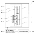
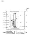
- FIG. 1A and FIG. 1B illustrate a laser module 100 in accordance with a first embodiment of the present invention.
- FIG. 1A illustrates a top view of the laser module 100 .
- FIG. 1B illustrates a cross sectional view taken along a line A-A of FIG. 1A .
- the laser module 100 has a temperature control device 20 , a mount carrier 30 and a wavelength-tunable semiconductor laser chip 40 .
- the mount carrier 30 may be a heat sink, a subcarrier, a submount or the like.
- a controller 200 and an electrical power supply 300 are provided out of the laser module 100 .
- the controller 200 controls an operation of the laser module 100 .
- the electrical power supply provides an electrical power to the laser module 100 .
- the controller 200 has a central processing unit (CPU), a read only memory (ROM), a random access memory (RAM) and so on.
- the laser module 100 , the controller 200 and the electrical power supply 300 are collectively referred to as a laser device.
- the temperature control device 20 controls the temperature of the wavelength-tunable semiconductor laser chip 40 .
- the temperature control device 20 is coupled to the electrical power supply 300 through a control terminal or the like (not shown).
- the temperature control device 20 controls the temperature of the wavelength-tunable semiconductor laser chip 40 by changing the temperature of the surface thereof according to an electrical power provided from the electrical power supply 300 .
- the mount carrier 30 is mounted on the temperature control device 20 .
- An electrode 31 and the wavelength-tunable semiconductor laser chip 40 are mounted on the mount carrier 30 .
- the electrode 31 is a metal pattern composed of a metal such as Au.
- An electrode 8 of the wavelength-tunable semiconductor laser chip 40 and the electrode 31 are coupled to each other with a plurality of wires 32 .
- the wire 32 is composed of a metal such as Au.
- the wire 32 has a diameter of approximately 20 ⁇ m.
- the electrode 31 is coupled to the electrical power supply 300 through a control terminal or the like (not shown).
- the wavelength-tunable semiconductor laser chip 40 has a structure in which a Sampled Grating Distributed Reflector (SG-DR) region A, a Sampled Grating Distributed Feedback (SG-DFB) region B and a Power Control (PC) region C are coupled in order.
- SG-DR Sampled Grating Distributed Reflector
- SG-DFB Sampled Grating Distributed Feedback
- PC Power Control
- the SG-DR region A has a structure in which an optical waveguide layer 3 , a cladding layer 5 and an insulating layer 6 are laminated on a substrate 1 in order and a heater 9 , a power electrode 10 and a ground electrode 11 are laminated on the insulating layer 6 .
- the SG-DFB region B has a structure in which an optical waveguide layer 4 , the cladding layer 5 , a contact layer 7 and the electrode 8 are laminated on the substrate 1 in order.
- the PC region C has a structure in which an optical waveguide layer 12 , the cladding layer 5 , a contact layer 13 and an electrode 14 are laminated on the substrate 1 in order.
- the substrate 1 and the cladding layer 5 of the SG-DR region A, the SG-DFB region B and the PC region C are a single layer formed as a unit respectively.
- the optical waveguide layers 3 , 4 and 12 are formed on a same plane and are optically coupled to each other.
- a low reflecting coating 15 is formed on end facet of the substrate 1 , the optical waveguide layer 3 and the cladding layer 5 at the SG-DR region A side.
- a low reflecting coating 16 is formed on end facet of the substrate 1 , the optical waveguide layer 12 and the cladding layer 5 at the PC region C side.
- Diffractive gratings 2 are formed at an interval in the optical waveguide layers 3 and 4 . The sampled grating is thus formed.
- the insulating layer 6 is further formed between the electrode 8 and the electrode 14 .
- the substrate 1 is, for example, a semiconductor substrate composed of InP.
- the optical waveguide layer 3 is, for example, composed of InGaAsP crystal having an absorption edge wavelength at shorter wavelengths side compared to the lasing wavelength.
- PL wavelength of the optical waveguide layer 3 is approximately 1.3 ⁇ m.
- the optical waveguide layer 4 is, for example, an active layer composed of InGaAsP crystal for amplifying a light of a desirable wavelength of a laser emission.
- the PL wavelength of the optical waveguide layer 4 is approximately 1.57 ⁇ m.
- the optical waveguide layer 12 is, for example, composed of InGaAsP crystal for changing the output of the emitted light by absorbing or amplifying a light.
- the PL wavelength of the optical waveguide layer 12 is approximately 1.57 ⁇ m.
- SG-DR segments are formed in the optical waveguide layer 3 .
- Other SG-DR segments are formed in the optical waveguide layer 4 .
- Three SG-DR segments are formed in the optical waveguide layer 3 and in the optical waveguide layer 4 respectively, in the embodiment.
- the SG-DR segment is a region in which one region having the diffractive grating 2 and one space region not having the diffractive grating 2 are combined in the optical waveguide layers 3 and 4 .
- the cladding layer 5 is composed of InP.
- the cladding layer 5 confines a laser light traveling in the optical waveguide layers 3 , 4 and 12 .
- the contact layers 7 and 13 are composed of InGaAsP crystal.
- the insulating layer 6 is a passivation film composed of an insulator such as SiN.
- the low reflecting coatings 15 and 16 are, for example, composed of a dielectric film including MgF 2 and TiON. The reflectivity of the low reflecting coatings 15 and 16 are, for example, less than 0.3%.
- the heater 9 is composed of such as NiCr and is provided above the SG-DR segment of the optical waveguide layer 3 .
- the power electrode 10 and the ground electrode 11 are coupled to the heater 9 .
- the power electrode 10 , the ground electrode 11 , the electrode 8 and the electrode 14 are composed of a conductive material such as Au.
- the power electrode 10 and the electrode 14 are coupled to the electrical power supply 300 through a control terminal or the like (not shown).
- the controller 200 controls the electrical power supply 300 so that a current is provided to the electrode 8 through the electrode 31 and the wires 32 .
- a light is generated in the optical waveguide layer 4 .
- the controller 200 controls the electrical power supply 300 so that a current is provided to the electrode 14 .
- the light propagates in the optical waveguide layers 3 and 4 , and is reflected and amplified repeatedly. Then, it causes lasing oscillation. A part of the emitted light is amplified or absorbed in the optical waveguide layer 12 and is emitted through the low reflecting coating 16 .
- the controller 200 can keep the output of the emitted light of the wavelength-tunable semiconductor laser chip 40 constant by controlling the current to be provided to the electrode 14 .
- the controller 200 controls the electrical power supply 300 so that a current is provided to the heater 9 .
- the controller 200 can control the temperature of the SG-DR segment of the SG-DR region A according to the current to be provided to the heater 9 .
- the refractive index of the SG-segment of the SG-DR region A is changed.
- a reflection peak wavelength of the optical waveguide layer 3 is changed. Accordingly, a laser light is emitted at a wavelength where the reflection peak wavelength of the SG-DR region A and the reflection peak wavelength of the SG-DFB region B are overlapped to each other. That is, it is possible to select a lasing wavelength of the wavelength-tunable semiconductor laser chip 40 .
- the controller 200 controls the electrical power supply 300 so that a current is provided to the temperature control device 20 .
- the controller 200 can control both temperatures of the optical waveguide layer 3 and the optical waveguide layer 4 according to the current to be provided to the temperature control device 20 .
- the refractive index of the optical waveguide layers 3 and 4 is changed.
- both of the reflection peak wavelengths of the optical waveguide layers 3 and 4 are changed. It is therefore possible to control the lasing wavelength of the wavelength-tunable semiconductor laser chip 40 . Accordingly, it is possible to control the lasing wavelength of the wavelength-tunable semiconductor laser chip 40 by controlling the current provided to the heater 9 and the temperature control device 20 .
- the temperature of the surface of the temperature control device 20 is substantially equal to that of the electrode 31 provided on the mount carrier 30 , because the mount carrier 30 is mounted on the temperature control device 20 .
- the heat generated in the temperature control device 20 is thus conducted to the electrode 8 from the electrode 31 through the wires 32 .
- the heat is conducted to the optical waveguide layer 4 from the electrode 8 .
- the optical waveguide layer 4 is heated from upper side and lower side thereof. Therefore, the temperature control device 20 can control the temperature of the optical waveguide layer 4 to be substantially constant.
- the temperature control device 20 can control the temperature of the optical waveguide layer 4 effectively, being less subjected to the heat of the heater 9 .
- connecting points between the wires 32 and the electrode 8 are at a substantially equal interval on the overall of the electrode 8 , because the thermal conductivity to the electrode 8 is improved in this case. It is preferable that the number of the wire 32 is larger.
- the wavelength-tunable semiconductor laser chip 40 corresponds to the optical semiconductor element.
- the mount carrier 30 corresponds to the area to be thermally conducted to the temperature control device.
- the wire 32 corresponds to the thermal conductive material.
- the SG-DFB region B corresponds to the first optical waveguide region.
- the SG-DR region A corresponds to the second optical waveguide region.
- the electrode 31 corresponds to the metal pattern.
- the area where the sampled diffractive grating 2 is formed in the optical waveguide layers 3 and 4 corresponds to the first region.
- the space region not having the sampled diffractive grating 2 corresponds to the second region.
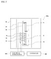
- FIG. 2 illustrates an overall structure of the laser module 100 a .
- the laser module 100 a differs from the laser module shown in FIG. 1A and FIG. 1B in a point that a thermal conductive portion 33 is provided on the mount carrier 30 .
- the same components have the same reference numerals in order to avoid a duplicated explanation.
- the thermal conductive portion 33 is composed of a material having a high thermal conductivity.
- the thermal conductive portion 33 may be composed of a conductive material or an insulating material. In the embodiment, the thermal conductive portion 33 is composed of a material such as Au.
- the thermal conductive portion 33 is not coupled to the electrical power supply 300 .
- the thermal conductive portion 33 does not provide electrical power to the electrode 8 but provides heat to the electrode 8 .
- the electrode 31 is coupled to the electrode 8 with at least one wire 32 .
- the thermal conductive portion 33 is coupled to the electrode 8 with at least one wire 32 .
- the heat is conducted to the electrode 8 from the electrode 31 and the thermal conductive portion 33 through the wires 32 .
- the temperature control device 20 can control the temperature of the optical waveguide layer 4 effectively.
- the wires 32 may not provide an electrical power to the electrode 8 .
- the effect of the present invention is obtained when the wire 32 conducts the heat generated in the temperature control device 20 to the electrode 8 .
- the thermal conductive portion 33 corresponds to the metal pattern.
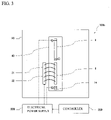
- FIG. 3 illustrates an overall structure of the laser module 100 b .
- the laser module 100 b differs from the laser module 100 shown in FIG. 1A and FIG. 1B in a point that the electrode 31 and the wavelength-tunable semiconductor laser chip 40 are mounted directly on the temperature control device 20 not through the mount carrier 30 .
- the same components have the same reference numerals in order to avoid a duplicated explanation.
- the heat generated in the temperature control device 20 is conducted directly to the wavelength-tunable semiconductor laser chip 40 . Further the heat is conducted directly to the electrode 31 , and is conducted to the electrode 8 through the wires 32 . And the temperature control device 20 can control the temperature of the optical waveguide layer 4 effectively.
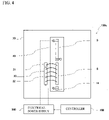
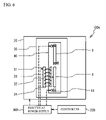
- FIG. 4 illustrates an overall structure of the laser module 100 c .
- the laser module 100 c differs from the laser module 100 shown in FIG. 1A and FIG. 1B in a point that the electrode 31 and the wavelength-tunable semiconductor laser chip 40 are mounted directly on the temperature control device 20 and the thermal conductive portion 33 is provided on the temperature control device 20 .
- the same components have the same reference numerals in order to avoid a duplicated explanation.
- the heat generated in the temperature control device 20 is conducted directly to the wavelength-tunable semiconductor laser chip 40 . Further the heat is conducted directly to the electrode 31 and the thermal conductive portion 33 , and is conducted to the electrode 8 through the wires 32 . And the temperature control device 20 can control the temperature of the optical waveguide layer 4 effectively.
- FIG. 5 illustrates an overall structure of the laser module 100 d .
- the laser module 100 d differs from the laser module 100 a shown in FIG. 2 in a point that a metal pattern 34 is provided on an upper face of the SG-DFB region B.
- the metal pattern 34 is electrically coupled to the optical waveguide layer 4 .
- the metal pattern 34 is coupled to the thermal conductive portion 33 with one or more than one wire 32 .
- the same components have the same reference numerals in order to avoid a duplicated explanation.
- heat is conducted to the metal pattern 34 from the thermal conductive portion 33 through the wires 32 .
- the temperature control device 20 can control the temperature of the optical waveguide layer 4 effectively.
- the metal pattern 34 corresponds to the area electrically coupled to the first optical waveguide region.
- FIG. 6 illustrates an overall structure of the laser module 100 e .
- the laser module 100 e is different from the laser module 100 shown in FIG. 1A and FIG. 1B in a point that the metal pattern 34 is provided on the upper face of the SG-DFB region B and is electrically conducted to the electrode 8 .
- the metal pattern 34 is electrically coupled to the optical waveguide layer 4 .
- the metal pattern 34 is coupled to the thermal conductive portion 33 with the wires 32 .
- the same components have the same reference numerals in order to avoid a duplicated explanation.
- the metal pattern 34 has a length larger than half of that of the optical waveguide layer 4 in an optical axis direction of the optical waveguide layer 4 . It is possible to provide heat to the optical waveguide layer 4 because the length of the metal pattern 34 is sufficiently large.
- FIG. 7 illustrates an overall structure of the laser module 100 f .
- the laser module 100 f is different from the laser module 100 e shown in FIG. 6 in a point that the metal pattern 34 is arranged at the optical waveguide layer 3 side with respect to a center of the optical waveguide layer 4 .
- the same components have the same reference numerals in order to avoid a duplicated explanation. In this case, it is possible to control the temperature of an area that is subjected to the heat from the heater 9 .
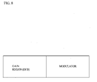
- the optical semiconductor device in accordance with the present invention is not limited to the SG-DR region or the SG-DFB region, although the SG-DR region and the SG-DFB region are an example of the optical semiconductor device in the above embodiments.
- the present invention may be applied to other optical semiconductor device that has a heater controlling a temperature of an optical waveguide layer.
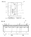
- FIG. 8 illustrates an example where the present invention is applied to a modulator. As shown in FIG. 8 , it is possible to provide heat to an upper face of the modulator of an optical semiconductor element from a heating portion such as a temperature control device through a wire, the optical semiconductor element having a gain portion and the modulator, the gain portion having a heater on a surface thereof, the modulator not having a heater on a surface thereof.
- a heating portion such as a temperature control device
Landscapes
- Physics & Mathematics (AREA)
- Condensed Matter Physics & Semiconductors (AREA)
- General Physics & Mathematics (AREA)
- Electromagnetism (AREA)
- Optics & Photonics (AREA)
- Semiconductor Lasers (AREA)
Abstract
Description
- 1. Field of the Invention
- This invention generally relates to an optical semiconductor element and an optical semiconductor device.
- 2. Description of the Related Art
- Generally, a wavelength-tunable semiconductor laser has a gain for a laser emission and can select a wavelength of the laser. There are some methods of selecting a-wavelength. For example, the methods include a method of changing a resonant wavelength of loss or gain by changing a refractive index or angle of a diffractive grating or an etalon provided in a laser cavity. And the methods include a method of changing a resonant wavelength of the laser cavity by changing an optical length in the laser cavity (refractive index or a physical length of the laser cavity).
- The method of changing the refractive index has an advantage in reliability or manufacturing cost, because a mechanical operating portion is not necessary being different from the method of changing the angle or length. The refractive index changing method includes changing a temperature of an optical waveguide, changing a carrier density in the optical waveguide by providing a current, and so on. A semiconductor laser having a Sampled Grating Distributed Reflector (SG-DR) is supposed as a wavelength tunable semiconductor laser that changes a temperature of an optical waveguide, where the SG-DR has a wavelength selection function.
- In this semiconductor laser, if a reflection spectrum of a plurality of SG-DR regions (reflection region) is controlled preferably, a predetermined wavelength can be selected with a vernier effect. That is, this semiconductor laser emits a laser at a wavelength where reflection peaks of two SG-DR regions are overlapped with each other. It is therefore possible to select the lasing wavelength by controlling each of the reflection peaks of the SG-DR regions.
- Generally, a heater is provided on a surface of one of the SG-DR regions. It is possible to change the temperature of an optical waveguide of the SG-DR region where the heater is provided, with heat generated by the heater. As a result, a refractive index of the optical waveguide is changed. Accordingly, it is possible to select a reflection peak wavelength of the SG-DR region where the heater is provided, by controlling the heating value of the heater.
- And it is possible to control the lasing wavelength to be a desirable one by controlling the refractive index of the optical waveguide of the SG-DR segments, with use of a temperature control device providing heat to whole of a semiconductor laser. And so, Japanese Patent Application Publication No. 9-92934 (hereinafter referred to as Document 1) discloses a method of controlling a lasing wavelength of the semiconductor laser by providing an electrical power to a heater and a temperature control device separately.
- However, it is apprehended that the temperature of an SG-DR region not having a heater is changed, when heating value of the heater is large. In this case, the lasing wavelength is off from a desirable one. In the semiconductor laser disclosed in
Document 1, an active region (a gain region) and a DBR region (a reflecting region) having a heater are adjacent to each other. As is the case of the conventional art, if the heating value of the heater is large, the temperature of the active region not having the heater is changed. Therefore, the lasing wavelength is off from a desirable one in the semiconductor laser disclosed inDocument 1. - The present invention provides an optical semiconductor element and an optical semiconductor device that can control a lasing wavelength accurately.
- According to an aspect of the present invention, preferably, there is provided an optical semiconductor device including an optical semiconductor element, a metal pattern and at least one thermal conductive material. The optical semiconductor element has a first optical waveguide region and a second optical waveguide region. The second optical waveguide region is optically coupled to the first optical waveguide region and has a heater for changing a refractive index of the second optical waveguide region. The metal pattern is provided on an area to be thermally coupled to a temperature control device. The thermal conductive material couples the metal pattern with an upper face of the first optical waveguide region of the optical semiconductor element. The thermal conductive material is electrically separated from the first optical waveguide region.
- With the above-mentioned configuration, heat is conducted to the first optical waveguide region through the thermal conductive material from the metal pattern that is provided on the area to be thermally coupled to the temperature control device. In this case, the first optical waveguide region is heated from a connecting point with the thermal conductive material and from the area to be thermally coupled to the temperature control device. It is therefore possible to control the temperature of the first optical waveguide region effectively in the optical semiconductor device, being less subjected to the heat of the heater. Accordingly, it is possible to control a lasing wavelength.
- According to another aspect of the present invention, preferably, there is provided an optical semiconductor device including an optical semiconductor element, a metal pattern and at least one thermal conductive material. The optical semiconductor element has a first optical waveguide region and a second optical waveguide region. The second optical waveguide region is optically coupled to the first optical waveguide region and has a heater for changing a refractive index of the second optical waveguide region. The metal pattern is provided on an area to be thermally coupled to a temperature control device. The thermal conductive material couples the metal pattern with an upper face of the first optical waveguide region of the optical semiconductor element. The thermal conductive material is electrically coupled to the first optical waveguide region.
- With the above-mentioned configuration, heat is conducted to the first optical waveguide region through the thermal conductive material from the metal pattern that is provided on the area to be thermally coupled to the temperature control device. In this case, the first optical waveguide region is heated from a connecting point with the thermal conductive material and from the area to be thermally coupled to the temperature control device. It is therefore possible to control the temperature of the first optical waveguide region effectively in the optical semiconductor device, being less subjected to the heat of the heater. Accordingly, it is possible to control a lasing wavelength.
- According to another aspect of the present invention, preferably, there is provided an optical semiconductor device including an optical semiconductor element, a metal pattern and a plurality of thermal conductive material. The optical semiconductor element has a first optical waveguide region and a second optical waveguide region. The second optical waveguide region is optically coupled to the first optical waveguide region and has a heater for changing a refractive index of the second optical waveguide region. The metal pattern is provided on an area to be thermally coupled to a temperature control device. The thermal conductive material couples the metal pattern with an upper face of the first optical waveguide region of the optical semiconductor element. The thermal conductive material is electrically coupled to the first optical waveguide region.
- With the above-mentioned configuration, heat is conducted to the first optical waveguide region through the thermal conductive material from the metal pattern that is provided on the area to be thermally coupled to the temperature control device. In this case, the first optical waveguide region is heated from a connecting point with the thermal conductive material and from the area to be thermally coupled to the temperature control device. It is therefore possible to control the temperature of the first optical waveguide region effectively in the optical semiconductor device, being less subjected to the heat of the heater. Accordingly, it is possible to control a lasing wavelength.
- According to another aspect of the present invention, preferably, there is provided an optical semiconductor device including an optical semiconductor element, a metal pattern and at least one thermal conductive material. The optical semiconductor element has a first optical waveguide region and a second optical waveguide region. The second optical waveguide region is optically coupled to the first optical waveguide region and has a heater for changing a refractive index of the second optical waveguide region. The metal pattern is provided on an area to be thermally coupled to a temperature control device. The thermal conductive material couples the metal pattern with an upper face of the first optical waveguide region of the optical semiconductor element. The thermal conductive material is at the second optical waveguide region side with respect to a center of the first optical waveguide region.
- With the above-mentioned configuration, heat is conducted to the first optical waveguide region through the thermal conductive material from the metal pattern that is provided on the area to be thermally coupled to the temperature control device. In this case, the first optical waveguide region is heated from a connecting point with the thermal conductive material and from the area to be thermally coupled to the temperature control device. It is therefore possible to control the temperature of the first optical waveguide region effectively in the optical semiconductor device, being less subjected to the heat of the heater. Accordingly, it is possible to-control a lasing wavelength.
- According to another aspect of the present invention, preferably, there is provided an optical semiconductor element including a first optical waveguide region, a second optical waveguide region and a metal pattern. The second optical waveguide region is optically coupled to the first optical waveguide region and has a heater for changing a refractive index of the second optical waveguide region. The metal pattern is provided on an upper face of the first optical waveguide region and has a length larger than half of that of the first optical waveguide region in an optical axis direction of the first optical waveguide region.
- With the above-mentioned configuration, heat is conducted to the first optical waveguide region from a heating portion such as a temperature control device when the metal pattern is thermally coupled to the heating portion. In this case, the first optical waveguide region is heated from the connecting points and the heating portion. It is therefore possible to control the temperature of the first optical waveguide region effectively in the optical semiconductor element, being less subjected to the heat of the heater. Accordingly, it is possible to control a lasing wavelength accurately. In addition, it is possible to conduct heat to the first optical waveguide region effectively because the metal pattern has a large length.
- According to another aspect of the present invention, preferably, there is provided an optical semiconductor element including a first optical waveguide region, a second optical waveguide region and a metal pattern. The second optical waveguide region is optically coupled to the first optical waveguide region and has a heater for changing a refractive index of the second optical waveguide region. The metal pattern is provided on an upper face of the first optical waveguide region at the second optical waveguide region side with respect to a center of the first optical waveguide region.
- With the above-mentioned configuration, heat is conducted to the first optical waveguide region from a heating portion such as a temperature control device when the metal pattern is thermally coupled to the heating portion. In this case, the first optical waveguide region is heated from the connecting points and the heating portion. It is therefore possible to control the temperature of the first optical waveguide region effectively in the optical semiconductor element, being less subjected to the heat of the heater. Accordingly, it is possible to control a lasing wavelength accurately. In addition, it is possible to control the temperature of an area of the first optical waveguide region subjected to the heat of the heater.
- Preferred embodiments of the present invention will be described in detail with reference to the following drawings, wherein:
-
FIG. 1A andFIG. 1B illustrate a laser module in accordance with a first embodiment of the present invention; -
FIG. 2 illustrates an overall structure of a laser module in accordance with a second embodiment of the present invention; -
FIG. 3 illustrates an overall structure of a laser module in accordance with a third embodiment of the present invention; -
FIG. 4 illustrates an overall structure of a laser module in accordance with a fourth embodiment of the present invention; -
FIG. 5 illustrates an overall structure of a laser module in accordance with a fifth embodiment of the present invention; -
FIG. 6 illustrates an overall structure of a laser module in accordance with a sixth embodiment of the present invention; -
FIG. 7 illustrates an overall structure of a laser module in accordance with a seventh embodiment of the present invention; and -
FIG. 8 illustrates an example where the present invention is applied to another optical semiconductor element. - A description will now be given, with reference to the accompanying drawings, of embodiments of the present invention.
-
FIG. 1A andFIG. 1B illustrate alaser module 100 in accordance with a first embodiment of the present invention.FIG. 1A illustrates a top view of thelaser module 100.FIG. 1B illustrates a cross sectional view taken along a line A-A ofFIG. 1A . As shown inFIG. 1A , thelaser module 100 has atemperature control device 20, amount carrier 30 and a wavelength-tunablesemiconductor laser chip 40. Themount carrier 30 may be a heat sink, a subcarrier, a submount or the like. Acontroller 200 and anelectrical power supply 300 are provided out of thelaser module 100. Thecontroller 200 controls an operation of thelaser module 100. The electrical power supply provides an electrical power to thelaser module 100. Thecontroller 200 has a central processing unit (CPU), a read only memory (ROM), a random access memory (RAM) and so on. Thelaser module 100, thecontroller 200 and theelectrical power supply 300 are collectively referred to as a laser device. - The
temperature control device 20 controls the temperature of the wavelength-tunablesemiconductor laser chip 40. Thetemperature control device 20 is coupled to theelectrical power supply 300 through a control terminal or the like (not shown). Thetemperature control device 20 controls the temperature of the wavelength-tunablesemiconductor laser chip 40 by changing the temperature of the surface thereof according to an electrical power provided from theelectrical power supply 300. Themount carrier 30 is mounted on thetemperature control device 20. Anelectrode 31 and the wavelength-tunablesemiconductor laser chip 40 are mounted on themount carrier 30. - The
electrode 31 is a metal pattern composed of a metal such as Au. Anelectrode 8 of the wavelength-tunablesemiconductor laser chip 40 and theelectrode 31 are coupled to each other with a plurality ofwires 32. Thewire 32 is composed of a metal such as Au. Thewire 32 has a diameter of approximately 20 μm. Theelectrode 31 is coupled to theelectrical power supply 300 through a control terminal or the like (not shown). - As shown in
FIG. 1B , the wavelength-tunablesemiconductor laser chip 40 has a structure in which a Sampled Grating Distributed Reflector (SG-DR) region A, a Sampled Grating Distributed Feedback (SG-DFB) region B and a Power Control (PC) region C are coupled in order. - The SG-DR region A has a structure in which an
optical waveguide layer 3, acladding layer 5 and an insulatinglayer 6 are laminated on asubstrate 1 in order and aheater 9, apower electrode 10 and aground electrode 11 are laminated on the insulatinglayer 6. The SG-DFB region B has a structure in which anoptical waveguide layer 4, thecladding layer 5, acontact layer 7 and theelectrode 8 are laminated on thesubstrate 1 in order. The PC region C has a structure in which anoptical waveguide layer 12, thecladding layer 5, a contact layer 13 and anelectrode 14 are laminated on thesubstrate 1 in order. Thesubstrate 1 and thecladding layer 5 of the SG-DR region A, the SG-DFB region B and the PC region C are a single layer formed as a unit respectively. Theoptical waveguide layers - A low reflecting
coating 15 is formed on end facet of thesubstrate 1, theoptical waveguide layer 3 and thecladding layer 5 at the SG-DR region A side. On the other hand, a low reflectingcoating 16 is formed on end facet of thesubstrate 1, theoptical waveguide layer 12 and thecladding layer 5 at the PC region C side.Diffractive gratings 2 are formed at an interval in theoptical waveguide layers layer 6 is further formed between theelectrode 8 and theelectrode 14. - The
substrate 1 is, for example, a semiconductor substrate composed of InP. Theoptical waveguide layer 3 is, for example, composed of InGaAsP crystal having an absorption edge wavelength at shorter wavelengths side compared to the lasing wavelength. PL wavelength of theoptical waveguide layer 3 is approximately 1.3 μm. Theoptical waveguide layer 4 is, for example, an active layer composed of InGaAsP crystal for amplifying a light of a desirable wavelength of a laser emission. The PL wavelength of theoptical waveguide layer 4 is approximately 1.57 μm. Theoptical waveguide layer 12 is, for example, composed of InGaAsP crystal for changing the output of the emitted light by absorbing or amplifying a light. The PL wavelength of theoptical waveguide layer 12 is approximately 1.57 μm. - SG-DR segments are formed in the
optical waveguide layer 3. Other SG-DR segments are formed in theoptical waveguide layer 4. Three SG-DR segments are formed in theoptical waveguide layer 3 and in theoptical waveguide layer 4 respectively, in the embodiment. Here, the SG-DR segment is a region in which one region having thediffractive grating 2 and one space region not having thediffractive grating 2 are combined in theoptical waveguide layers - The
cladding layer 5 is composed of InP. Thecladding layer 5 confines a laser light traveling in theoptical waveguide layers layer 6 is a passivation film composed of an insulator such as SiN. The low reflectingcoatings coatings - The
heater 9 is composed of such as NiCr and is provided above the SG-DR segment of theoptical waveguide layer 3. Thepower electrode 10 and theground electrode 11 are coupled to theheater 9. Thepower electrode 10, theground electrode 11, theelectrode 8 and theelectrode 14 are composed of a conductive material such as Au. Thepower electrode 10 and theelectrode 14 are coupled to theelectrical power supply 300 through a control terminal or the like (not shown). - Next, a description will be given of a controlling method of the
laser module 100. At first, thecontroller 200 controls theelectrical power supply 300 so that a current is provided to theelectrode 8 through theelectrode 31 and thewires 32. A light is generated in theoptical waveguide layer 4. And thecontroller 200 controls theelectrical power supply 300 so that a current is provided to theelectrode 14. The light propagates in theoptical waveguide layers optical waveguide layer 12 and is emitted through the low reflectingcoating 16. It is possible to control the gain or the absorptance of theoptical waveguide layer 12 with the current provided to theelectrode 14. Thecontroller 200 can keep the output of the emitted light of the wavelength-tunablesemiconductor laser chip 40 constant by controlling the current to be provided to theelectrode 14. - The
controller 200 controls theelectrical power supply 300 so that a current is provided to theheater 9. Thecontroller 200 can control the temperature of the SG-DR segment of the SG-DR region A according to the current to be provided to theheater 9. In this case, the refractive index of the SG-segment of the SG-DR region A is changed. And a reflection peak wavelength of theoptical waveguide layer 3 is changed. Accordingly, a laser light is emitted at a wavelength where the reflection peak wavelength of the SG-DR region A and the reflection peak wavelength of the SG-DFB region B are overlapped to each other. That is, it is possible to select a lasing wavelength of the wavelength-tunablesemiconductor laser chip 40. - The
controller 200 controls theelectrical power supply 300 so that a current is provided to thetemperature control device 20. Thecontroller 200 can control both temperatures of theoptical waveguide layer 3 and theoptical waveguide layer 4 according to the current to be provided to thetemperature control device 20. In this case, the refractive index of theoptical waveguide layers optical waveguide layers semiconductor laser chip 40. Accordingly, it is possible to control the lasing wavelength of the wavelength-tunablesemiconductor laser chip 40 by controlling the current provided to theheater 9 and thetemperature control device 20. - The temperature of the surface of the
temperature control device 20 is substantially equal to that of theelectrode 31 provided on themount carrier 30, because themount carrier 30 is mounted on thetemperature control device 20. The heat generated in thetemperature control device 20 is thus conducted to theelectrode 8 from theelectrode 31 through thewires 32. And the heat is conducted to theoptical waveguide layer 4 from theelectrode 8. Theoptical waveguide layer 4 is heated from upper side and lower side thereof. Therefore, thetemperature control device 20 can control the temperature of theoptical waveguide layer 4 to be substantially constant. Thetemperature control device 20 can control the temperature of theoptical waveguide layer 4 effectively, being less subjected to the heat of theheater 9. - It is preferable that connecting points between the
wires 32 and theelectrode 8 are at a substantially equal interval on the overall of theelectrode 8, because the thermal conductivity to theelectrode 8 is improved in this case. It is preferable that the number of thewire 32 is larger. - In the embodiment, the wavelength-tunable
semiconductor laser chip 40 corresponds to the optical semiconductor element. Themount carrier 30 corresponds to the area to be thermally conducted to the temperature control device. Thewire 32 corresponds to the thermal conductive material. The SG-DFB region B corresponds to the first optical waveguide region. The SG-DR region A corresponds to the second optical waveguide region. Theelectrode 31 corresponds to the metal pattern. The area where the sampleddiffractive grating 2 is formed in theoptical waveguide layers diffractive grating 2 corresponds to the second region. (Second embodiment) Next, a description will be given of alaser module 100 a in accordance with a second embodiment of the present invention.FIG. 2 illustrates an overall structure of thelaser module 100 a. As shown inFIG. 2 , thelaser module 100 a differs from the laser module shown inFIG. 1A andFIG. 1B in a point that a thermalconductive portion 33 is provided on themount carrier 30. The same components have the same reference numerals in order to avoid a duplicated explanation. - The thermal
conductive portion 33 is composed of a material having a high thermal conductivity. The thermalconductive portion 33 may be composed of a conductive material or an insulating material. In the embodiment, the thermalconductive portion 33 is composed of a material such as Au. The thermalconductive portion 33 is not coupled to theelectrical power supply 300. The thermalconductive portion 33 does not provide electrical power to theelectrode 8 but provides heat to theelectrode 8. Theelectrode 31 is coupled to theelectrode 8 with at least onewire 32. The thermalconductive portion 33 is coupled to theelectrode 8 with at least onewire 32. - In the embodiment, the heat is conducted to the
electrode 8 from theelectrode 31 and the thermalconductive portion 33 through thewires 32. Thetemperature control device 20 can control the temperature of theoptical waveguide layer 4 effectively. Thewires 32 may not provide an electrical power to theelectrode 8. The effect of the present invention is obtained when thewire 32 conducts the heat generated in thetemperature control device 20 to theelectrode 8. - In the embodiment, the thermal
conductive portion 33 corresponds to the metal pattern. - Next, a description will be given of a
laser module 100 b in accordance with a third embodiment of the present invention.FIG. 3 illustrates an overall structure of thelaser module 100 b. As shown inFIG. 3 , thelaser module 100 b differs from thelaser module 100 shown inFIG. 1A andFIG. 1B in a point that theelectrode 31 and the wavelength-tunablesemiconductor laser chip 40 are mounted directly on thetemperature control device 20 not through themount carrier 30. The same components have the same reference numerals in order to avoid a duplicated explanation. - In the embodiment, the heat generated in the
temperature control device 20 is conducted directly to the wavelength-tunablesemiconductor laser chip 40. Further the heat is conducted directly to theelectrode 31, and is conducted to theelectrode 8 through thewires 32. And thetemperature control device 20 can control the temperature of theoptical waveguide layer 4 effectively. - Next, a description will be given of a
laser module 100 c in accordance with a fourth embodiment of the present invention.FIG. 4 illustrates an overall structure of thelaser module 100 c. As shown inFIG. 4 , thelaser module 100 c differs from thelaser module 100 shown inFIG. 1A andFIG. 1B in a point that theelectrode 31 and the wavelength-tunablesemiconductor laser chip 40 are mounted directly on thetemperature control device 20 and the thermalconductive portion 33 is provided on thetemperature control device 20. The same components have the same reference numerals in order to avoid a duplicated explanation. - In the embodiment, the heat generated in the
temperature control device 20 is conducted directly to the wavelength-tunablesemiconductor laser chip 40. Further the heat is conducted directly to theelectrode 31 and the thermalconductive portion 33, and is conducted to theelectrode 8 through thewires 32. And thetemperature control device 20 can control the temperature of theoptical waveguide layer 4 effectively. - Next, a description will be given of a
laser module 100 d in accordance with a fifth embodiment of the present invention.FIG. 5 illustrates an overall structure of thelaser module 100 d. As shown inFIG. 5 , thelaser module 100 d differs from thelaser module 100 a shown inFIG. 2 in a point that ametal pattern 34 is provided on an upper face of the SG-DFB region B. Themetal pattern 34 is electrically coupled to theoptical waveguide layer 4. Themetal pattern 34 is coupled to the thermalconductive portion 33 with one or more than onewire 32. The same components have the same reference numerals in order to avoid a duplicated explanation. - In the embodiment, heat is conducted to the
metal pattern 34 from the thermalconductive portion 33 through thewires 32. And thetemperature control device 20 can control the temperature of theoptical waveguide layer 4 effectively. In the embodiment, themetal pattern 34 corresponds to the area electrically coupled to the first optical waveguide region. - Next, a description will be given of a
laser module 100 e in accordance with a sixth embodiment of the present invention.FIG. 6 illustrates an overall structure of thelaser module 100 e. As shown inFIG. 6 , thelaser module 100 e is different from thelaser module 100 shown inFIG. 1A andFIG. 1B in a point that themetal pattern 34 is provided on the upper face of the SG-DFB region B and is electrically conducted to theelectrode 8. Themetal pattern 34 is electrically coupled to theoptical waveguide layer 4. Themetal pattern 34 is coupled to the thermalconductive portion 33 with thewires 32. The same components have the same reference numerals in order to avoid a duplicated explanation. - In the embodiment, the
metal pattern 34 has a length larger than half of that of theoptical waveguide layer 4 in an optical axis direction of theoptical waveguide layer 4. It is possible to provide heat to theoptical waveguide layer 4 because the length of themetal pattern 34 is sufficiently large. - A description will be given of a
laser module 100 f in accordance with a seventh embodiment of the present invention.FIG. 7 illustrates an overall structure of thelaser module 100 f. As shown inFIG. 7 , thelaser module 100 f is different from thelaser module 100 e shown inFIG. 6 in a point that themetal pattern 34 is arranged at theoptical waveguide layer 3 side with respect to a center of theoptical waveguide layer 4. The same components have the same reference numerals in order to avoid a duplicated explanation. In this case, it is possible to control the temperature of an area that is subjected to the heat from theheater 9. - The optical semiconductor device in accordance with the present invention is not limited to the SG-DR region or the SG-DFB region, although the SG-DR region and the SG-DFB region are an example of the optical semiconductor device in the above embodiments. The present invention may be applied to other optical semiconductor device that has a heater controlling a temperature of an optical waveguide layer.
-
FIG. 8 illustrates an example where the present invention is applied to a modulator. As shown inFIG. 8 , it is possible to provide heat to an upper face of the modulator of an optical semiconductor element from a heating portion such as a temperature control device through a wire, the optical semiconductor element having a gain portion and the modulator, the gain portion having a heater on a surface thereof, the modulator not having a heater on a surface thereof. - While the above description constitutes the preferred embodiments of the present invention, it will be appreciated that the invention is susceptible of modification, variation and change without departing from the proper scope and fair meaning of the accompanying claims.
- The present invention is based on Japanese Patent Application No. 2006-100351 filed on Mar. 31, 2006, the entire disclosure of which is hereby incorporated by reference.
Claims (19)
Priority Applications (2)
| Application Number | Priority Date | Filing Date | Title |
|---|---|---|---|
| US12/314,350 US7656927B2 (en) | 2006-03-31 | 2008-12-09 | Optical semiconductor element and optical semiconductor device |
| US12/640,897 US20100091805A1 (en) | 2006-03-31 | 2009-12-17 | Optical semiconductor element and optical semiconductor device |
Applications Claiming Priority (2)
| Application Number | Priority Date | Filing Date | Title |
|---|---|---|---|
| JP2006-100351 | 2006-03-31 | ||
| JP2006100351A JP4772564B2 (en) | 2006-03-31 | 2006-03-31 | Optical semiconductor element and optical semiconductor device |
Related Child Applications (1)
| Application Number | Title | Priority Date | Filing Date |
|---|---|---|---|
| US12/314,350 Division US7656927B2 (en) | 2006-03-31 | 2008-12-09 | Optical semiconductor element and optical semiconductor device |
Publications (2)
| Publication Number | Publication Date |
|---|---|
| US20070228551A1 true US20070228551A1 (en) | 2007-10-04 |
| US7474684B2 US7474684B2 (en) | 2009-01-06 |
Family
ID=38557603
Family Applications (3)
| Application Number | Title | Priority Date | Filing Date |
|---|---|---|---|
| US11/730,260 Active US7474684B2 (en) | 2006-03-31 | 2007-03-30 | Optical semiconductor element and optical semiconductor device |
| US12/314,350 Expired - Fee Related US7656927B2 (en) | 2006-03-31 | 2008-12-09 | Optical semiconductor element and optical semiconductor device |
| US12/640,897 Abandoned US20100091805A1 (en) | 2006-03-31 | 2009-12-17 | Optical semiconductor element and optical semiconductor device |
Family Applications After (2)
| Application Number | Title | Priority Date | Filing Date |
|---|---|---|---|
| US12/314,350 Expired - Fee Related US7656927B2 (en) | 2006-03-31 | 2008-12-09 | Optical semiconductor element and optical semiconductor device |
| US12/640,897 Abandoned US20100091805A1 (en) | 2006-03-31 | 2009-12-17 | Optical semiconductor element and optical semiconductor device |
Country Status (2)
| Country | Link |
|---|---|
| US (3) | US7474684B2 (en) |
| JP (1) | JP4772564B2 (en) |
Cited By (2)
| Publication number | Priority date | Publication date | Assignee | Title |
|---|---|---|---|---|
| US10074959B2 (en) * | 2016-08-03 | 2018-09-11 | Emcore Corporation | Modulated laser source and methods of its fabrication and operation |
| US11479849B2 (en) * | 2019-06-03 | 2022-10-25 | Taiwan Semiconductor Manufacturing Company, Ltd. | Physical vapor deposition chamber with target surface morphology monitor |
Families Citing this family (3)
| Publication number | Priority date | Publication date | Assignee | Title |
|---|---|---|---|---|
| JP2007273644A (en) * | 2006-03-30 | 2007-10-18 | Eudyna Devices Inc | Optical semiconductor device, laser chip, and laser module |
| US20130070795A1 (en) * | 2011-09-16 | 2013-03-21 | Sumitomo Electric Industries, Ltd. | Method to switch emission wavelength of tunable laser diode |
| JP2014013823A (en) | 2012-07-04 | 2014-01-23 | Sumitomo Electric Ind Ltd | Method of controlling tunable semiconductor laser |
Citations (2)
| Publication number | Priority date | Publication date | Assignee | Title |
|---|---|---|---|---|
| US20020090011A1 (en) * | 2000-10-30 | 2002-07-11 | Bardia Pezeshki | Laser thermal tuning |
| US20030006225A1 (en) * | 2001-05-14 | 2003-01-09 | Fow-Sen Choa | Thermally tunable system |
Family Cites Families (11)
| Publication number | Priority date | Publication date | Assignee | Title |
|---|---|---|---|---|
| JPH05291693A (en) * | 1992-04-06 | 1993-11-05 | Mitsubishi Electric Corp | Heat dissipation method for semiconductor laser device |
| US5841799A (en) * | 1994-12-17 | 1998-11-24 | Canon Kabushiki Kaisha | Semiconductor laser, modulation method therefor and optical communication system using the same |
| JPH08172243A (en) * | 1994-12-17 | 1996-07-02 | Canon Inc | Optical transmitter and its modulating system |
| US5536085A (en) * | 1995-03-30 | 1996-07-16 | Northern Telecom Limited | Multi-wavelength gain-coupled distributed feedback laser array with fine tunability |
| JP2914248B2 (en) * | 1995-09-23 | 1999-06-28 | 日本電気株式会社 | Tunable semiconductor laser device |
| JPH10282373A (en) * | 1997-04-07 | 1998-10-23 | Oki Electric Ind Co Ltd | Optical module and method for forming optical module |
| JP3166836B2 (en) * | 1997-11-18 | 2001-05-14 | 日本電気株式会社 | Semiconductor laser |
| JP3618989B2 (en) * | 1997-12-24 | 2005-02-09 | 株式会社東芝 | Semiconductor laser device |
| JP2000312049A (en) * | 1999-04-27 | 2000-11-07 | Fuji Photo Film Co Ltd | Semiconductor optical function device |
| JP2001094200A (en) * | 1999-09-21 | 2001-04-06 | Hitachi Ltd | Semiconductor laser module |
| US7224708B2 (en) * | 2004-08-30 | 2007-05-29 | The Aerospace Corporation | Focused ion beam heater thermally tunable laser |
-
2006
- 2006-03-31 JP JP2006100351A patent/JP4772564B2/en not_active Expired - Lifetime
-
2007
- 2007-03-30 US US11/730,260 patent/US7474684B2/en active Active
-
2008
- 2008-12-09 US US12/314,350 patent/US7656927B2/en not_active Expired - Fee Related
-
2009
- 2009-12-17 US US12/640,897 patent/US20100091805A1/en not_active Abandoned
Patent Citations (2)
| Publication number | Priority date | Publication date | Assignee | Title |
|---|---|---|---|---|
| US20020090011A1 (en) * | 2000-10-30 | 2002-07-11 | Bardia Pezeshki | Laser thermal tuning |
| US20030006225A1 (en) * | 2001-05-14 | 2003-01-09 | Fow-Sen Choa | Thermally tunable system |
Cited By (3)
| Publication number | Priority date | Publication date | Assignee | Title |
|---|---|---|---|---|
| US10074959B2 (en) * | 2016-08-03 | 2018-09-11 | Emcore Corporation | Modulated laser source and methods of its fabrication and operation |
| US11479849B2 (en) * | 2019-06-03 | 2022-10-25 | Taiwan Semiconductor Manufacturing Company, Ltd. | Physical vapor deposition chamber with target surface morphology monitor |
| US12486566B2 (en) | 2019-06-03 | 2025-12-02 | Taiwan Semiconductor Manufacturing Company, Ltd. | Physical vapor deposition chamber with target surface morphology monitor |
Also Published As
| Publication number | Publication date |
|---|---|
| JP4772564B2 (en) | 2011-09-14 |
| US20090103585A1 (en) | 2009-04-23 |
| US7474684B2 (en) | 2009-01-06 |
| JP2007273883A (en) | 2007-10-18 |
| US20100091805A1 (en) | 2010-04-15 |
| US7656927B2 (en) | 2010-02-02 |
Similar Documents
| Publication | Publication Date | Title |
|---|---|---|
| US8563991B2 (en) | Optical semiconductor device, laser chip and laser module | |
| KR100799782B1 (en) | Tunable semiconductor laser device, manufacturing method thereof, and gas detecting device using same | |
| US7388894B2 (en) | Hybrid MOPA having narrowband oscillator and amplifier with integrated optical coupling | |
| US7515779B2 (en) | Optical semiconductor device | |
| US8194710B2 (en) | Semiconductor laser with heater | |
| US7656927B2 (en) | Optical semiconductor element and optical semiconductor device | |
| US7362782B2 (en) | Optical semiconductor device and controlling method of the same | |
| JP4629022B2 (en) | LASER DEVICE, LASER MODULE, AND SEMICONDUCTOR LASER | |
| US6901086B2 (en) | Stack-type diode laser device | |
| US9025628B2 (en) | Semiconductor laser | |
| CN101479897B (en) | Semiconductor light emitting element and variable wavelength laser light source | |
| JP2007273694A (en) | Optical semiconductor device | |
| JP5303580B2 (en) | Optical semiconductor device, laser chip and laser module | |
| JP5303581B2 (en) | Optical semiconductor device | |
| US10348055B2 (en) | Folded waveguide structure semiconductor laser |
Legal Events
| Date | Code | Title | Description |
|---|---|---|---|
| AS | Assignment |
Owner name: EUDYNA DEVICES INC., JAPAN Free format text: ASSIGNMENT OF ASSIGNORS INTEREST;ASSIGNORS:ISHIKAWA, TSUTOMU;FUJII, TAKUYA;REEL/FRAME:019195/0450 Effective date: 20070316 |
|
| FEPP | Fee payment procedure |
Free format text: PAYOR NUMBER ASSIGNED (ORIGINAL EVENT CODE: ASPN); ENTITY STATUS OF PATENT OWNER: LARGE ENTITY |
|
| STCF | Information on status: patent grant |
Free format text: PATENTED CASE |
|
| FPAY | Fee payment |
Year of fee payment: 4 |
|
| FPAY | Fee payment |
Year of fee payment: 8 |
|
| MAFP | Maintenance fee payment |
Free format text: PAYMENT OF MAINTENANCE FEE, 12TH YEAR, LARGE ENTITY (ORIGINAL EVENT CODE: M1553); ENTITY STATUS OF PATENT OWNER: LARGE ENTITY Year of fee payment: 12 |