US20070188198A1 - Device and system for controlling current to a load - Google Patents
Device and system for controlling current to a load Download PDFInfo
- Publication number
- US20070188198A1 US20070188198A1 US11/525,407 US52540706A US2007188198A1 US 20070188198 A1 US20070188198 A1 US 20070188198A1 US 52540706 A US52540706 A US 52540706A US 2007188198 A1 US2007188198 A1 US 2007188198A1
- Authority
- US
- United States
- Prior art keywords
- current
- load
- recited
- power sources
- parallel power
- Prior art date
- Legal status (The legal status is an assumption and is not a legal conclusion. Google has not performed a legal analysis and makes no representation as to the accuracy of the status listed.)
- Granted
Links
Images


Classifications
-
- G—PHYSICS
- G06—COMPUTING OR CALCULATING; COUNTING
- G06F—ELECTRIC DIGITAL DATA PROCESSING
- G06F1/00—Details not covered by groups G06F3/00 - G06F13/00 and G06F21/00
- G06F1/26—Power supply means, e.g. regulation thereof
- G06F1/263—Arrangements for using multiple switchable power supplies, e.g. battery and AC
-
- H—ELECTRICITY
- H03—ELECTRONIC CIRCUITRY
- H03K—PULSE TECHNIQUE
- H03K17/00—Electronic switching or gating, i.e. not by contact-making and –breaking
- H03K17/08—Modifications for protecting switching circuit against overcurrent or overvoltage
- H03K17/082—Modifications for protecting switching circuit against overcurrent or overvoltage by feedback from the output to the control circuit
- H03K17/0822—Modifications for protecting switching circuit against overcurrent or overvoltage by feedback from the output to the control circuit in field-effect transistor switches
-
- H—ELECTRICITY
- H03—ELECTRONIC CIRCUITRY
- H03K—PULSE TECHNIQUE
- H03K17/00—Electronic switching or gating, i.e. not by contact-making and –breaking
- H03K17/22—Modifications for ensuring a predetermined initial state when the supply voltage has been applied
Definitions
- a device and system for controlling load currents are disclosed and, more particularly, a device and system for controlling currents to a load from plural parallel power sources having hot swap capabilities.
- Hot swapping refers to the ability of an electronic system or network of electronic systems to continue operating without interrupting the delivery of power to the system or network of systems after modules or components of the system or network, e.g., a hard drive, a power supply, a CD-ROM drive, and the like, are removed and replaced.
- modules or components of the system or network e.g., a hard drive, a power supply, a CD-ROM drive, and the like.
- current to a load is ramped ON (or, alternatively, during extraction, current to a load is ramped OFF) in a controlled, linear manner to prevent disturbances on the power supply feed. This feature allows modules or components to be inserted into or extracted from a powered system without having to shut off power.
- Hot swap devices often include a current control function that prevents current to a load from exceeding a programmed maximum level. Thus, hot swapping reduces system down time and improves system availability.
- ATCA Advanced Telecom Computer Architecture
- the standardized ATCA hardware platform includes a plurality of interconnected circuit boards and a chassis portion, or card shelf. By convention, each card shelf provides 14 or 16 slots for cards.
- MicroTCA A scaled-down and less expensive version of the ATCA is the MicroTCA.
- MicroTCA supports smaller scale applications and is less powerful than ACTA but, otherwise, is similar in many respects.
- a major difference between the MicroTCA and the ATCA is that the MicroTCA does not include a carrier board.
- both the ATCA and the MicroTCA are compatible with Advanced Mezzanine Cards (“AMCs”).
- AMCs are designed to be installed and to operate in a MicroTCA chassis or, alternatively, in an ATCA carrier board.
- AMCs are fully-managed intelligent cards that require hotswap protection. Hotswap circuitry for AMCs, however, is not on the AMC boards but, rather, is part of the MicroTCA power module or, alternatively, is part of the ATCA carrier board.
- load current the maximum current available to the load
- the current level typically, is unacceptably large.
- conventional power sources are not coupled in parallel in conjunction with ATCAs, MicroTCAs, and/or AMCs.
- a device for controlling current from a plurality of parallel power sources to a load includes a load line for delivering a current to the load; a current sensing device, e.g., a low-impedance resistor or a current splitter, for measuring the current being delivered to the load; and a common sense element, e.g., a high-impedance resistor, for adjusting the current being delivered to the load by each of the plurality of parallel power sources.
- the load line is electrically coupled to and disposed between the output port of each of the plurality of parallel power sources and the load.
- the common sense element is electrically coupled to the current sense port of each of the plurality of parallel power sources.
- each of the power sources has a hot swap capability for delivering inrush currents and the load is an advanced mezzanine card (“AMC”) that is operationally associated with an Advanced Telecom Computer Architecture (“ATCA”) or a Micro Telecom Computer Architecture (“Micro TCA”).
- AMC advanced mezzanine card
- ATCA Advanced Telecom Computer Architecture
- Micro TCA Micro Telecom Computer Architecture
- the current sensing device includes an operating amplifier or other means that outputs a current to the common sense element via a current sense port.
- the current output by the operating amplifier or other means is directly proportional to the current being delivered to-the load by the respective power source.
- a system for controlling current to a load e.g., an AMC that is operationally associated with an ATCA or a Micro TCA, is also disclosed.
- the system includes a plurality of parallel power sources that deliver current to the load and the current-controlling device described above.
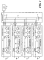
- FIG. 1 is a diagram of plural parallel power sources having internal inrush controllers and control systems in accordance with the present invention
- FIG. 2 is a circuit diagram of a current-sharing control system in accordance with the present invention.
- FIG. 3 is a circuit diagram of an alternative current-sharing control system in accordance with the present invention.
- a high-availability system for controlling the total load current from plural power sources having internal inrush controllers arranged in parallel to a load is disclosed.
- the system 10 is shown to include a current-controlling device 15 and plural parallel power sources 12 a to 12 d.
- the current-controlling device 15 is electrically-coupled to and disposed serially between the plural parallel power sources 12 a to 12 d and a load 19 , e.g., an AMC.
- the current-controlling device 15 includes plural input/output (“I/O”) interfaces 16 , or connections, and a high-impedance, common sense element 11 , e.g., a high-impedance, common sense resistor. More particularly, each I/O interface 16 includes at least two ports 16 a and 16 b. The first ports 16 a of each I/O interface are connected to the output ports 22 of each of the plural power sources 12 a to 12 d and to a load line 13 . The second ports 16 b of each I/O interface are connected to the current sense ports 24 of each of the plural power sources 12 a to 12 d and to a sense resistor line 17 .
- the load line 13 leads to the load 19 and the sense resistor line 17 leads to a high-impedance, e.g., 10 k ⁇ , common sense element 11 .
- Each of the plural power sources 12 a to 12 d includes a hot swap inrush current controller 25 , a current sensing device or current sensor 20 , and a switching or control device 28 .
- Hot swap inrush current controllers 25 are well known in the art and will not be discussed in detail herein.
- the current sensor 20 and/or the switching or control device 28 are described and shown herein as components of the power sources 12 a to 12 d, those skilled in the art will appreciate that the current sensor 20 and/or the switching or control device 28 , alternatively, can be external to the power sources 12 a to 12 d, which is to say they can be components of the current-controlling device 15 .
- a power source 12 with a current sensor 20 in accordance with the present invention will be described.
- the timing and amount of current delivery to the load 19 from each power source 12 is controlled by the switching or control device 28 , e.g., a field effect transistor (“FET”), a bi-polar junction transistor (“BJT”), a voltage OR diode, and the like.
- FET field effect transistor
- BJT bi-polar junction transistor
- voltage OR diode e.g., a voltage OR diode
- the switching device 28 of the invention e.g., a field effect transistor (“FET”), a bi-polar junction transistor (“BJT”), a voltage OR diode, and the like.
- FET field effect transistor
- BJT bi-polar junction transistor
- MOSFET metal-oxide semiconductor FET
- MOSFETs 28 are three-terminal switching devices having a gate (G) electrode, a drain (D) electrode, and a source (S) electrode. Representative MOSFETs 28 can be n-channel or p-channel switching devices. MOSFETs 28 include an input voltage port, e.g., between the gate (G) and source (S) electrodes, and an output voltage port, e.g., between the drain (D) and source (S) electrodes. The input voltage port controls the flow of current between the drain (D) and the source (S) electrodes.
- v gs when the gate-source input or biasing voltage (v gs ) is below a gate-source threshold voltage, there is no current flowing between the drain (D) and the source (S) electrodes. However, when the gate-source input or biasing voltage (v gs ) exceeds the threshold voltage, a controllable current (i d ) flows between the drain (D) and the source (S) electrodes. Once the gate-source input or biasing voltage (v gs ) saturates the MOSFET 28 , a steady, constant or nearly constant current (i d ) is delivered.
- the amount of current (i d ) flowing between the drain (D) and source (S) electrodes which is to say, the amount of current (id) flowing from the power source 12 to the load 19 , depends on the input or biasing voltage (v gs ) and on the output port voltage (v ds ).
- v gs input or biasing voltage
- v ds output port voltage
- current (i d ) passes through the switching device(s) 28 of the power source 12 , it first passes through a low-impedance, e.g., 7 m ⁇ , sense element 27 , e.g., a sense resistor in the current sensor 20 . Consistent with Ohm's law, current passing through a resistive element causes a voltage drop that is proportional to the current (in amperes) times the resistance (in ohms).
- the current sensor 20 is structured and arranged to compare the source voltage immediately upstream of the sense element 27 with the voltage immediately downstream of the sense element 27 , i.e., after the voltage drop.
- the voltage drop, or potential loss, through the relatively low-impedance, sense element 27 is proportional to the magnitude of the current passing through the sense element 27 .
- the greater the current passing through the sense element 27 the greater the voltage drop and vice versa.
- the current sensor 20 further includes a means, such as an operating amplifier (“OPAMP”) 29 , through which the upstream and downstream voltage levels are fed.
- OPAMP operating amplifier
- the upstream voltage level is input into the positive input port (+) of OPAMP 29 via current sensor input port 21 and the downstream voltage level is input into the negative input port ( ⁇ ) of OPAMP 29 via current sensor input port 23 .
- the OPAMP 29 determines the voltage change (drop or loss) across the sense element 27 , e.g., by subtracting the downstream voltage level at the negative input port ( ⁇ ) from the upstream voltage level at the positive input port (+).
- the OPAMP 29 outputs a current (I OUT ) that is proportional to the voltage drop, e.g., in milli-volts (“mV”) and, more specifically, that is proportional to the amount of current (i d ) that the particular power source 12 is delivering to the load 19 .
- a current (I OUT ) is proportional to the voltage drop, e.g., in milli-volts (“mV”) and, more specifically, that is proportional to the amount of current (i d ) that the particular power source 12 is delivering to the load 19 .
- the output current (I OUT ) is equal to 10 ⁇ A per mV.
- the output current (I OUT ) from the OPAMP 29 of each power source 12 is transmitted to ground via a current sense port 24 , the sense element line 17 , and the high-impedance, common sense element 11 .
- the current-controlling device 10 measures the voltage drop associated with the output currents (I OUT ) passing through the high-impedance common sense element 11 and adjusts the amount of current (i d ) from each power source 12 going to the load 19 , e.g., by increasing or decreasing the gate-source or biasing voltage (v gs ) of the switching device(s) 28 .
- a predetermined maximum allowable current (I MAX ) and/or a predetermined maximum allowable voltage (V MAX ) for the high-impedance common sense element 11 can be fixed.
- FIG. 3 Another system 10 having an alternative current sensor 30 is shown in FIG. 3 .
- the timing and amount of current (i d ) delivered to the load 19 from each power source 12 is controlled by a switching device 28 , e.g., a field effect transistor, a bi-polar junction transistor, a voltage OR diode, and the like.
- the alternative current sensor 30 includes a current splitter 35 .
- the current splitter 35 includes a relatively low-impedance, e.g., 7 m ⁇ , sense element 27 , which is structured and arranged in parallel with a relatively high-impedance, e.g., 10 k ⁇ , current-controlling element (R CL ) 32 .
- the impedance of the current-controlling element 32 is much greater than the impedance of the sense element 27 . Consequently, the amount of current (i d ) passing through sense element 27 is greater than the amount of current (i CL ) passing through the current-controlling element 32 .
- Whether or not current (i CL ) passes through the current-controlling resistor 32 is controlled by a switching or control device 38 , e.g., a FET, a BJT, a voltage OR diode, and the like, in the current sensor 30 .
- the current sensor 30 includes a means, such as an operating amplifier (“OPAMP”) or comparator 39 , that provides a gate-source input or biasing voltage (V GATE ) to the MOSFET 38 , to control the amount of current (i CL ) passing through the current-controlling element 32 vis-à-vis the amount of current passing through the sense element 27 to the load 19 .
- OPAMP operating amplifier
- V GATE gate-source input or biasing voltage
- the OPAMP 39 is structured and arranged to compare the line voltage at input port 31 , i.e., immediately after the current-controlling element 32 , with the voltage at input port 33 , i.e., immediately downstream of the sense element 27 . Instead of directly outputting current to the common sense element 11 , the OPAMP 39 , instead, outputs an input or biasing voltage (V GATE ) to the switching device 38 .
- V GATE input or biasing voltage
- the output current (I OUT ) from each power source 12 passes to ground via the current sense port 24 , the sense element line 17 , and the high-impedance common sense element 11 to ground.
- the current-controlling device 10 measures the voltage drop associated with the output currents (I OUT ) passing through the high-impedance common sense element 11 and adjusts the amount of current (i d ) from each power source 12 going to the load 19 , e.g., by increasing or decreasing the gate input or biasing voltage (v gs ) of the switching device 28 and/or by increasing or decreasing the gate input or biasing voltage (v gs ) of the switching device 38 in the current sensor 30 .
- a predetermined maximum allowable current (I MAX ) and/or a predetermined maximum allowable voltage (V MAX ) for the high-impedance common sense element 11 can be fixed.
Landscapes
- Engineering & Computer Science (AREA)
- Theoretical Computer Science (AREA)
- Power Engineering (AREA)
- Physics & Mathematics (AREA)
- General Engineering & Computer Science (AREA)
- General Physics & Mathematics (AREA)
- Control Of Voltage And Current In General (AREA)
Abstract
Description
- This application claims the benefit of U.S. provisional patent application No. 60/772,628 filed on Feb. 13, 2006.
- (Not Applicable)
- A device and system for controlling load currents are disclosed and, more particularly, a device and system for controlling currents to a load from plural parallel power sources having hot swap capabilities.
- “Hot swapping” refers to the ability of an electronic system or network of electronic systems to continue operating without interrupting the delivery of power to the system or network of systems after modules or components of the system or network, e.g., a hard drive, a power supply, a CD-ROM drive, and the like, are removed and replaced. Typically, during a hot swapping insertion, current to a load is ramped ON (or, alternatively, during extraction, current to a load is ramped OFF) in a controlled, linear manner to prevent disturbances on the power supply feed. This feature allows modules or components to be inserted into or extracted from a powered system without having to shut off power. Hot swap devices often include a current control function that prevents current to a load from exceeding a programmed maximum level. Thus, hot swapping reduces system down time and improves system availability.
- High availability (“HA”) systems are particularly desirable, especially in telecommunications. For example, the Advanced Telecom Computer Architecture (“ATCA”) provides a common, high availability hardware platform for telecommunications systems. The standardized ATCA hardware platform includes a plurality of interconnected circuit boards and a chassis portion, or card shelf. By convention, each card shelf provides 14 or 16 slots for cards.
- A scaled-down and less expensive version of the ATCA is the MicroTCA. MicroTCA supports smaller scale applications and is less powerful than ACTA but, otherwise, is similar in many respects. A major difference between the MicroTCA and the ATCA is that the MicroTCA does not include a carrier board.
- Advantageously, both the ATCA and the MicroTCA are compatible with Advanced Mezzanine Cards (“AMCs”). AMCs are designed to be installed and to operate in a MicroTCA chassis or, alternatively, in an ATCA carrier board. AMCs are fully-managed intelligent cards that require hotswap protection. Hotswap circuitry for AMCs, however, is not on the AMC boards but, rather, is part of the MicroTCA power module or, alternatively, is part of the ATCA carrier board.
- To improve the reliability of HA systems, redundant, parallel power sources are desirable. However, with plural power sources in parallel, the maximum current available to the load (“load current”) is the sum of the output currents of each of the plural power sources. If all power sources are delivering current, the current level, typically, is unacceptably large. As a result, conventional power sources are not coupled in parallel in conjunction with ATCAs, MicroTCAs, and/or AMCs.
- Therefore, it would be desirable to provide a system for controlling current levels from plural parallel power sources to a load and a device for the same. It would also be desirable to provide a device for use with plural parallel power sources that controls current rather than load shares. BRIEF SUMMARY OF THE INVENTION
- A device for controlling current from a plurality of parallel power sources to a load is disclosed. The device includes a load line for delivering a current to the load; a current sensing device, e.g., a low-impedance resistor or a current splitter, for measuring the current being delivered to the load; and a common sense element, e.g., a high-impedance resistor, for adjusting the current being delivered to the load by each of the plurality of parallel power sources. The load line is electrically coupled to and disposed between the output port of each of the plurality of parallel power sources and the load. The common sense element is electrically coupled to the current sense port of each of the plurality of parallel power sources.
- In one aspect, each of the power sources has a hot swap capability for delivering inrush currents and the load is an advanced mezzanine card (“AMC”) that is operationally associated with an Advanced Telecom Computer Architecture (“ATCA”) or a Micro Telecom Computer Architecture (“Micro TCA”).
- In another aspect, the current sensing device includes an operating amplifier or other means that outputs a current to the common sense element via a current sense port. The current output by the operating amplifier or other means is directly proportional to the current being delivered to-the load by the respective power source.
- A system for controlling current to a load, e.g., an AMC that is operationally associated with an ATCA or a Micro TCA, is also disclosed. The system includes a plurality of parallel power sources that deliver current to the load and the current-controlling device described above.
- The foregoing and other objects, features, and advantages of the invention will be apparent from the following Detailed Description of the Invention in conjunction with the Drawings of which:
-
FIG. 1 is a diagram of plural parallel power sources having internal inrush controllers and control systems in accordance with the present invention; -
FIG. 2 is a circuit diagram of a current-sharing control system in accordance with the present invention; and -
FIG. 3 is a circuit diagram of an alternative current-sharing control system in accordance with the present invention. - This application claims the benefit of U.S. provisional patent application No. 60/772,628 filed on Feb. 13, 2006, which is incorporated herein in its entirety by reference.
- A high-availability system for controlling the total load current from plural power sources having internal inrush controllers arranged in parallel to a load is disclosed. Referring to
FIG. 1 , the system 10 is shown to include a current-controlling device 15 and pluralparallel power sources 12 a to 12 d. The current-controlling device 15 is electrically-coupled to and disposed serially between the pluralparallel power sources 12 a to 12 d and aload 19, e.g., an AMC. - The current-controlling device 15 includes plural input/output (“I/O”)
interfaces 16, or connections, and a high-impedance,common sense element 11, e.g., a high-impedance, common sense resistor. More particularly, each I/O interface 16 includes at least twoports first ports 16 a of each I/O interface are connected to theoutput ports 22 of each of theplural power sources 12 a to 12 d and to aload line 13. Thesecond ports 16 b of each I/O interface are connected to thecurrent sense ports 24 of each of theplural power sources 12 a to 12 d and to asense resistor line 17. Theload line 13 leads to theload 19 and thesense resistor line 17 leads to a high-impedance, e.g., 10 kΩ,common sense element 11. - Each of the
plural power sources 12 a to 12 d includes a hot swap inrushcurrent controller 25, a current sensing device orcurrent sensor 20, and a switching orcontrol device 28. Hot swap inrushcurrent controllers 25 are well known in the art and will not be discussed in detail herein. Furthermore, although, thecurrent sensor 20 and/or the switching orcontrol device 28 are described and shown herein as components of thepower sources 12a to 12d, those skilled in the art will appreciate that thecurrent sensor 20 and/or the switching orcontrol device 28, alternatively, can be external to thepower sources 12 a to 12 d, which is to say they can be components of the current-controlling device 15. - Referring to
FIG. 2 , apower source 12 with acurrent sensor 20 in accordance with the present invention will be described. The timing and amount of current delivery to theload 19 from eachpower source 12 is controlled by the switching orcontrol device 28, e.g., a field effect transistor (“FET”), a bi-polar junction transistor (“BJT”), a voltage OR diode, and the like. For convenience, the remainder of this disclosure will describe theswitching device 28 of the invention as a FET or, more particularly, a metal-oxide semiconductor FET (“MOSFET”). -
MOSFETs 28 are three-terminal switching devices having a gate (G) electrode, a drain (D) electrode, and a source (S) electrode.Representative MOSFETs 28 can be n-channel or p-channel switching devices.MOSFETs 28 include an input voltage port, e.g., between the gate (G) and source (S) electrodes, and an output voltage port, e.g., between the drain (D) and source (S) electrodes. The input voltage port controls the flow of current between the drain (D) and the source (S) electrodes. - More specifically, when the gate-source input or biasing voltage (vgs) is below a gate-source threshold voltage, there is no current flowing between the drain (D) and the source (S) electrodes. However, when the gate-source input or biasing voltage (vgs) exceeds the threshold voltage, a controllable current (id) flows between the drain (D) and the source (S) electrodes. Once the gate-source input or biasing voltage (vgs) saturates the
MOSFET 28, a steady, constant or nearly constant current (id) is delivered. - The amount of current (id) flowing between the drain (D) and source (S) electrodes, which is to say, the amount of current (id) flowing from the
power source 12 to theload 19, depends on the input or biasing voltage (vgs) and on the output port voltage (vds). By increasing (or decreasing) the input or biasing voltage (vgs), one can increase (or decrease) the source current (id) from thepower source 12 to theload 19 until theMOSFET 28 becomes saturated. Here again, once the gate-source input or biasing voltage (vgs) saturates theMOSFET 28, a steady, constant or nearly constant current (id) is delivered. - As current (id) passes through the switching device(s) 28 of the
power source 12, it first passes through a low-impedance, e.g., 7 mΩ,sense element 27, e.g., a sense resistor in thecurrent sensor 20. Consistent with Ohm's law, current passing through a resistive element causes a voltage drop that is proportional to the current (in amperes) times the resistance (in ohms). Thecurrent sensor 20 is structured and arranged to compare the source voltage immediately upstream of thesense element 27 with the voltage immediately downstream of thesense element 27, i.e., after the voltage drop. - Consistent with Ohm's and Kirchoff's laws, the voltage drop, or potential loss, through the relatively low-impedance,
sense element 27 is proportional to the magnitude of the current passing through thesense element 27. Thus, the greater the current passing through thesense element 27, the greater the voltage drop and vice versa. - The
current sensor 20 further includes a means, such as an operating amplifier (“OPAMP”) 29, through which the upstream and downstream voltage levels are fed. For example, the upstream voltage level is input into the positive input port (+) ofOPAMP 29 via currentsensor input port 21 and the downstream voltage level is input into the negative input port (−) ofOPAMP 29 via currentsensor input port 23. TheOPAMP 29 determines the voltage change (drop or loss) across thesense element 27, e.g., by subtracting the downstream voltage level at the negative input port (−) from the upstream voltage level at the positive input port (+). - The
OPAMP 29 outputs a current (IOUT) that is proportional to the voltage drop, e.g., in milli-volts (“mV”) and, more specifically, that is proportional to the amount of current (id) that theparticular power source 12 is delivering to theload 19. For illustrative purposes only, inFIG. 2 , the output current (IOUT) is equal to 10 μA per mV. - The output current (IOUT) from the
OPAMP 29 of eachpower source 12 is transmitted to ground via acurrent sense port 24, thesense element line 17, and the high-impedance,common sense element 11. The current-controlling device 10 measures the voltage drop associated with the output currents (IOUT) passing through the high-impedancecommon sense element 11 and adjusts the amount of current (id) from eachpower source 12 going to theload 19, e.g., by increasing or decreasing the gate-source or biasing voltage (vgs) of the switching device(s) 28. To prevent over-current from being delivered to theload 19, a predetermined maximum allowable current (IMAX) and/or a predetermined maximum allowable voltage (VMAX) for the high-impedancecommon sense element 11 can be fixed. - Another system 10 having an alternative
current sensor 30 is shown inFIG. 3 . As with the previously describedcurrent sensor 20, the timing and amount of current (id) delivered to theload 19 from eachpower source 12 is controlled by aswitching device 28, e.g., a field effect transistor, a bi-polar junction transistor, a voltage OR diode, and the like. I In contrast with the previously describedcurrent sensor 20, the alternativecurrent sensor 30 includes a current splitter 35. The current splitter 35 includes a relatively low-impedance, e.g., 7 mΩ,sense element 27, which is structured and arranged in parallel with a relatively high-impedance, e.g., 10 kΩ, current-controlling element (RCL) 32. The impedance of the current-controllingelement 32 is much greater than the impedance of thesense element 27. Consequently, the amount of current (id) passing throughsense element 27 is greater than the amount of current (iCL) passing through the current-controllingelement 32. - As with
current sensor 20, when the input or biasing voltage between the gate (G) and source (S) electrodes (vgs) of theswitching device 28 exceeds the threshold voltage, current (id) passes through thesense element 27 to theload 19. The magnitude of the current (id) to theload 19 for eachpower source 12 is controllable, e.g., by controlling the magnitude of the gate-source input or biasing voltage (vgs). - As the name implies, with the current splitter 35, while a first portion of the total source current (id) passes through the
sense element 27 to theload 19, a second portion of the total source current (iCL) passes through the current-controllingresistor 32. Current (iCL) passing through the current-controllingelement 32 is output to thecommon sense element 11, e.g., via thecurrent sense port 24. - Whether or not current (iCL) passes through the current-controlling
resistor 32 is controlled by a switching orcontrol device 38, e.g., a FET, a BJT, a voltage OR diode, and the like, in thecurrent sensor 30. More particularly, thecurrent sensor 30 includes a means, such as an operating amplifier (“OPAMP”) orcomparator 39, that provides a gate-source input or biasing voltage (VGATE) to theMOSFET 38, to control the amount of current (iCL) passing through the current-controllingelement 32 vis-à-vis the amount of current passing through thesense element 27 to theload 19. - The
OPAMP 39 is structured and arranged to compare the line voltage atinput port 31, i.e., immediately after the current-controllingelement 32, with the voltage atinput port 33, i.e., immediately downstream of thesense element 27. Instead of directly outputting current to thecommon sense element 11, theOPAMP 39, instead, outputs an input or biasing voltage (VGATE) to theswitching device 38. - When the input or biasing voltage (VGATE) exceeds the threshold voltage of the
switching device 38, current (iCL) through the current-controllingelement 32 is delivered to thecommon sense element 11 to ground, e.g., via thecurrent sense port 24. TheOPAMP 39 will continue to provide gate voltages (VGATE) and theswitching device 38 will continue to deliver current (iCL) to thecommon sense element 11 until the voltage across thesense element 27 and the voltage across the current controllingelement 32 are equal. Moreover, the amount of current (iCL) to thecommon sense element 11 can be controlled by controlling the magnitude of the gate voltages (VGATE). - The output current (IOUT) from each
power source 12 passes to ground via thecurrent sense port 24, thesense element line 17, and the high-impedancecommon sense element 11 to ground. The current-controlling device 10 measures the voltage drop associated with the output currents (IOUT) passing through the high-impedancecommon sense element 11 and adjusts the amount of current (id) from eachpower source 12 going to theload 19, e.g., by increasing or decreasing the gate input or biasing voltage (vgs) of theswitching device 28 and/or by increasing or decreasing the gate input or biasing voltage (vgs) of theswitching device 38 in thecurrent sensor 30. To prevent over-current from being delivered to theload 19, a predetermined maximum allowable current (IMAX) and/or a predetermined maximum allowable voltage (VMAX) for the high-impedancecommon sense element 11 can be fixed. - It will be apparent to those of ordinary skill in the art that modifications to and variations of the above-described system and method may be made without departing from the inventive concepts described herein. Accordingly, the invention should not be controlled except by the scope and spirit of the appended claims.
Claims (27)
Priority Applications (1)
| Application Number | Priority Date | Filing Date | Title |
|---|---|---|---|
| US11/525,407 US7739525B2 (en) | 2006-02-13 | 2006-09-22 | Device and system for controlling parallel power sources coupled to a load |
Applications Claiming Priority (2)
| Application Number | Priority Date | Filing Date | Title |
|---|---|---|---|
| US77262806P | 2006-02-13 | 2006-02-13 | |
| US11/525,407 US7739525B2 (en) | 2006-02-13 | 2006-09-22 | Device and system for controlling parallel power sources coupled to a load |
Publications (2)
| Publication Number | Publication Date |
|---|---|
| US20070188198A1 true US20070188198A1 (en) | 2007-08-16 |
| US7739525B2 US7739525B2 (en) | 2010-06-15 |
Family
ID=38367729
Family Applications (1)
| Application Number | Title | Priority Date | Filing Date |
|---|---|---|---|
| US11/525,407 Active 2028-12-23 US7739525B2 (en) | 2006-02-13 | 2006-09-22 | Device and system for controlling parallel power sources coupled to a load |
Country Status (1)
| Country | Link |
|---|---|
| US (1) | US7739525B2 (en) |
Cited By (17)
| Publication number | Priority date | Publication date | Assignee | Title |
|---|---|---|---|---|
| US20100007217A1 (en) * | 2008-07-14 | 2010-01-14 | Texas Instruments Incorporated | Minimum loss and wiring circuit and method for paralleling hot swap controllers |
| CN101833295A (en) * | 2010-04-23 | 2010-09-15 | 烽火通信科技股份有限公司 | System for realizing thermal simulation and control of ATCA subframe |
| US20130286525A1 (en) * | 2012-04-27 | 2013-10-31 | Netapp, Inc. | Systems and Methods Providing Current Protection to an Electronic System |
| CN103713719A (en) * | 2012-10-09 | 2014-04-09 | 纬创资通股份有限公司 | Current distribution system, current distribution method and computer system thereof |
| US20140152280A1 (en) * | 2011-10-05 | 2014-06-05 | Analog Devices, Inc. | Apparatus and method for distributing power-up power dissipation |
| US20200133380A1 (en) * | 2018-10-31 | 2020-04-30 | Dell Products, Lp | Method and Apparatus to Distribute Current Indicator to Multiple End-Points |
| CN112134448A (en) * | 2020-08-04 | 2020-12-25 | 华为技术有限公司 | Servers and Data Centers |
| US10951051B2 (en) | 2018-10-30 | 2021-03-16 | Dell Products, L.P. | Method and apparatus to charge power assist unit |
| US10948959B2 (en) | 2018-10-31 | 2021-03-16 | Dell Products, L.P. | Method and apparatus to control power assist unit |
| US10983577B2 (en) | 2018-10-30 | 2021-04-20 | Dell Products L.P. | Method and apparatus to provide dynamic regulation of power assist unit output based on active profile |
| US10990149B2 (en) | 2018-10-31 | 2021-04-27 | Dell Products L.P. | Method and apparatus for providing peak optimized power supply unit |
| US11114838B2 (en) * | 2016-07-19 | 2021-09-07 | Abb Schweiz Ag | Ideal diode with active reverse voltage protection |
| US11126250B2 (en) | 2018-10-30 | 2021-09-21 | Dell Products L.P. | Method and apparatus for extending power hold-up with power assist unit |
| US11144105B2 (en) | 2018-10-30 | 2021-10-12 | Dell Products L.P. | Method and apparatus to provide platform power peak limiting based on charge of power assist unit |
| US11199894B2 (en) | 2018-10-30 | 2021-12-14 | Dell Products L.P. | Method and apparatus for providing high bandwidth capacitor circuit in power assist unit |
| US11228202B2 (en) * | 2019-02-06 | 2022-01-18 | Hewlett Packard Enterprise Development Lp | Synchronized standby startup of power supplies with current injection |
| US20240410793A1 (en) * | 2023-06-12 | 2024-12-12 | Shenzhen Fulian Fugui Precision Industry Co., Ltd. | Control method for heat dissipation verification device, heat dissipation verification device and system |
Families Citing this family (4)
| Publication number | Priority date | Publication date | Assignee | Title |
|---|---|---|---|---|
| US8654550B2 (en) * | 2010-06-17 | 2014-02-18 | Hewlett-Packard Development Company, L.P. | Circulating current detection for redundant power supply |
| DE202010010716U1 (en) | 2010-07-27 | 2010-12-16 | Zippy Technology Corp., Hsin-Tien | Adjustment system for multiple power sources |
| US8331117B2 (en) | 2010-08-04 | 2012-12-11 | Zippy Technology Corp. | Multiple power supplies balance system |
| CN111864722A (en) * | 2019-04-25 | 2020-10-30 | 康普技术有限责任公司 | Current sharing control circuit, power supply system and current sharing control method |
Citations (7)
| Publication number | Priority date | Publication date | Assignee | Title |
|---|---|---|---|---|
| US6055647A (en) * | 1997-08-15 | 2000-04-25 | Compaq Computer Corporation | Method and apparatus for determining computer system power supply redundancy level |
| US6421215B1 (en) * | 1999-10-08 | 2002-07-16 | Sun Microsystems, Inc. | Power overload protection for a system unit |
| US6448672B1 (en) * | 2000-02-29 | 2002-09-10 | 3Com Corporation | Intelligent power supply control for electronic systems requiring multiple voltages |
| US7030771B2 (en) * | 2003-03-12 | 2006-04-18 | Sun Microsystems, Inc. | System and method to provide hot-swap status indication in a computer system having redundant power supplies |
| US7170194B2 (en) * | 2002-10-15 | 2007-01-30 | Powerdsine, Ltd. | Configurable multiple power source system |
| US7265955B2 (en) * | 2002-10-24 | 2007-09-04 | Knorr-Bremse Systeme Fuer Nutzfahrzeuge Gmbh | Protective circuit for analog sensors |
| US7272733B2 (en) * | 2003-09-26 | 2007-09-18 | Hewlett-Packard Development Company, L.P. | Method of providing dynamic power redundancy based on a difference of current power units and currently needed power units |
-
2006
- 2006-09-22 US US11/525,407 patent/US7739525B2/en active Active
Patent Citations (7)
| Publication number | Priority date | Publication date | Assignee | Title |
|---|---|---|---|---|
| US6055647A (en) * | 1997-08-15 | 2000-04-25 | Compaq Computer Corporation | Method and apparatus for determining computer system power supply redundancy level |
| US6421215B1 (en) * | 1999-10-08 | 2002-07-16 | Sun Microsystems, Inc. | Power overload protection for a system unit |
| US6448672B1 (en) * | 2000-02-29 | 2002-09-10 | 3Com Corporation | Intelligent power supply control for electronic systems requiring multiple voltages |
| US7170194B2 (en) * | 2002-10-15 | 2007-01-30 | Powerdsine, Ltd. | Configurable multiple power source system |
| US7265955B2 (en) * | 2002-10-24 | 2007-09-04 | Knorr-Bremse Systeme Fuer Nutzfahrzeuge Gmbh | Protective circuit for analog sensors |
| US7030771B2 (en) * | 2003-03-12 | 2006-04-18 | Sun Microsystems, Inc. | System and method to provide hot-swap status indication in a computer system having redundant power supplies |
| US7272733B2 (en) * | 2003-09-26 | 2007-09-18 | Hewlett-Packard Development Company, L.P. | Method of providing dynamic power redundancy based on a difference of current power units and currently needed power units |
Cited By (24)
| Publication number | Priority date | Publication date | Assignee | Title |
|---|---|---|---|---|
| US20100007217A1 (en) * | 2008-07-14 | 2010-01-14 | Texas Instruments Incorporated | Minimum loss and wiring circuit and method for paralleling hot swap controllers |
| US8847438B2 (en) * | 2008-07-14 | 2014-09-30 | Texas Instruments Incorporated | Minimum loss and wiring circuit and method for paralleling hot swap controllers |
| CN101833295A (en) * | 2010-04-23 | 2010-09-15 | 烽火通信科技股份有限公司 | System for realizing thermal simulation and control of ATCA subframe |
| US20140152280A1 (en) * | 2011-10-05 | 2014-06-05 | Analog Devices, Inc. | Apparatus and method for distributing power-up power dissipation |
| US9405307B2 (en) * | 2011-10-05 | 2016-08-02 | Analog Devices, Inc. | Apparatus and method for distributing power-up power dissipation |
| US10185340B2 (en) | 2011-10-05 | 2019-01-22 | Analog Devices, Inc. | Apparatus and method for distributing power-up power dissipation |
| US20130286525A1 (en) * | 2012-04-27 | 2013-10-31 | Netapp, Inc. | Systems and Methods Providing Current Protection to an Electronic System |
| US9036314B2 (en) * | 2012-04-27 | 2015-05-19 | Netapp, Inc. | Systems and methods providing current protection to an electronic system |
| CN103713719A (en) * | 2012-10-09 | 2014-04-09 | 纬创资通股份有限公司 | Current distribution system, current distribution method and computer system thereof |
| US11114838B2 (en) * | 2016-07-19 | 2021-09-07 | Abb Schweiz Ag | Ideal diode with active reverse voltage protection |
| US10951051B2 (en) | 2018-10-30 | 2021-03-16 | Dell Products, L.P. | Method and apparatus to charge power assist unit |
| US11126250B2 (en) | 2018-10-30 | 2021-09-21 | Dell Products L.P. | Method and apparatus for extending power hold-up with power assist unit |
| US11199894B2 (en) | 2018-10-30 | 2021-12-14 | Dell Products L.P. | Method and apparatus for providing high bandwidth capacitor circuit in power assist unit |
| US11144105B2 (en) | 2018-10-30 | 2021-10-12 | Dell Products L.P. | Method and apparatus to provide platform power peak limiting based on charge of power assist unit |
| US10983577B2 (en) | 2018-10-30 | 2021-04-20 | Dell Products L.P. | Method and apparatus to provide dynamic regulation of power assist unit output based on active profile |
| US10990149B2 (en) | 2018-10-31 | 2021-04-27 | Dell Products L.P. | Method and apparatus for providing peak optimized power supply unit |
| US20200133380A1 (en) * | 2018-10-31 | 2020-04-30 | Dell Products, Lp | Method and Apparatus to Distribute Current Indicator to Multiple End-Points |
| US10948959B2 (en) | 2018-10-31 | 2021-03-16 | Dell Products, L.P. | Method and apparatus to control power assist unit |
| US10852808B2 (en) * | 2018-10-31 | 2020-12-01 | Dell Products, L.P. | Method and apparatus to distribute current indicator to multiple end-points |
| US11599182B2 (en) | 2018-10-31 | 2023-03-07 | Dell Products L.P. | Method and apparatus to distribute current indicator to multiple end-points |
| US11228202B2 (en) * | 2019-02-06 | 2022-01-18 | Hewlett Packard Enterprise Development Lp | Synchronized standby startup of power supplies with current injection |
| CN112134448A (en) * | 2020-08-04 | 2020-12-25 | 华为技术有限公司 | Servers and Data Centers |
| US20240410793A1 (en) * | 2023-06-12 | 2024-12-12 | Shenzhen Fulian Fugui Precision Industry Co., Ltd. | Control method for heat dissipation verification device, heat dissipation verification device and system |
| US12566109B2 (en) * | 2023-06-12 | 2026-03-03 | Shenzhen Fulian Fugui Precision Industry Co., Ltd. | Control method for heat dissipation verification device, heat dissipation verification device and system |
Also Published As
| Publication number | Publication date |
|---|---|
| US7739525B2 (en) | 2010-06-15 |
Similar Documents
| Publication | Publication Date | Title |
|---|---|---|
| US7739525B2 (en) | Device and system for controlling parallel power sources coupled to a load | |
| KR101336054B1 (en) | Method and system for voltage independent power supply load sharing | |
| JP5121850B2 (en) | DC high power distribution assembly | |
| CA2785593C (en) | Redundant module with symmetrical current paths | |
| US7636011B2 (en) | Controller for ORing field effect transistor | |
| US9917437B2 (en) | Hot swap controller with individually controlled parallel current paths | |
| US6807039B2 (en) | Inrush limiter circuit | |
| CN107612299B (en) | dynamic switching of current control devices in a load current controller | |
| TW200928984A (en) | CPU core voltage supply | |
| US8040647B2 (en) | System and method for protection against loss of battery in reverse battery protected devices | |
| US9787180B2 (en) | High side switch with current limit feedback | |
| US20200028345A1 (en) | Methods and apparatus to prevent undesired triggering of short circuit or over current protection | |
| JP2021502049A5 (en) | ||
| US20120182661A1 (en) | Overcurrent protection device | |
| US20090256616A1 (en) | Hot swap controller with zero loaded charge pump | |
| US20150061620A1 (en) | Current control circuit | |
| US7102338B2 (en) | Multi-sense voltage regulator | |
| US10164423B2 (en) | Method and system for ground plane isolation | |
| US10873327B2 (en) | Hot swap controller with multiple current limits | |
| US8582267B2 (en) | System and method to limit in-rush current | |
| JP2024541585A (en) | Technique for limiting overshoot after dropout condition in voltage regulators - Patents.com | |
| US6496345B1 (en) | Current regulation with low on resistance in overdriven mode | |
| CN120185336A (en) | Power input multiplexer | |
| KR101702220B1 (en) | Inrush current limiting circuit even for a load with power switch | |
| CN113726129A (en) | Power management circuit and electronic equipment |
Legal Events
| Date | Code | Title | Description |
|---|---|---|---|
| AS | Assignment |
Owner name: TEXAS INSTRUMENTS INCORPORATED, TEXAS Free format text: ASSIGNMENT OF ASSIGNORS INTEREST;ASSIGNOR:BIRD, JAMES G.;REEL/FRAME:018337/0194 Effective date: 20060915 Owner name: TEXAS INSTRUMENTS INCORPORATED,TEXAS Free format text: ASSIGNMENT OF ASSIGNORS INTEREST;ASSIGNOR:BIRD, JAMES G.;REEL/FRAME:018337/0194 Effective date: 20060915 |
|
| STCF | Information on status: patent grant |
Free format text: PATENTED CASE |
|
| FPAY | Fee payment |
Year of fee payment: 4 |
|
| MAFP | Maintenance fee payment |
Free format text: PAYMENT OF MAINTENANCE FEE, 8TH YEAR, LARGE ENTITY (ORIGINAL EVENT CODE: M1552) Year of fee payment: 8 |
|
| MAFP | Maintenance fee payment |
Free format text: PAYMENT OF MAINTENANCE FEE, 12TH YEAR, LARGE ENTITY (ORIGINAL EVENT CODE: M1553); ENTITY STATUS OF PATENT OWNER: LARGE ENTITY Year of fee payment: 12 |