US20070075884A1 - Calibration of a redundant number system successive approximation analog-to-digital converter - Google Patents
Calibration of a redundant number system successive approximation analog-to-digital converter Download PDFInfo
- Publication number
- US20070075884A1 US20070075884A1 US11/537,872 US53787206A US2007075884A1 US 20070075884 A1 US20070075884 A1 US 20070075884A1 US 53787206 A US53787206 A US 53787206A US 2007075884 A1 US2007075884 A1 US 2007075884A1
- Authority
- US
- United States
- Prior art keywords
- weight vector
- analog
- converter
- vector
- vectors
- Prior art date
- Legal status (The legal status is an assumption and is not a legal conclusion. Google has not performed a legal analysis and makes no representation as to the accuracy of the status listed.)
- Granted
Links
Images


Classifications
-
- H—ELECTRICITY
- H03—ELECTRONIC CIRCUITRY
- H03M—CODING; DECODING; CODE CONVERSION IN GENERAL
- H03M1/00—Analogue/digital conversion; Digital/analogue conversion
- H03M1/10—Calibration or testing
- H03M1/1009—Calibration
- H03M1/1033—Calibration over the full range of the converter, e.g. for correcting differential non-linearity
- H03M1/1038—Calibration over the full range of the converter, e.g. for correcting differential non-linearity by storing corrected or correction values in one or more digital look-up tables
-
- H—ELECTRICITY
- H03—ELECTRONIC CIRCUITRY
- H03M—CODING; DECODING; CODE CONVERSION IN GENERAL
- H03M1/00—Analogue/digital conversion; Digital/analogue conversion
- H03M1/10—Calibration or testing
- H03M1/1009—Calibration
- H03M1/1033—Calibration over the full range of the converter, e.g. for correcting differential non-linearity
-
- H—ELECTRICITY
- H03—ELECTRONIC CIRCUITRY
- H03M—CODING; DECODING; CODE CONVERSION IN GENERAL
- H03M1/00—Analogue/digital conversion; Digital/analogue conversion
- H03M1/06—Continuously compensating for, or preventing, undesired influence of physical parameters
- H03M1/0617—Continuously compensating for, or preventing, undesired influence of physical parameters characterised by the use of methods or means not specific to a particular type of detrimental influence
- H03M1/0675—Continuously compensating for, or preventing, undesired influence of physical parameters characterised by the use of methods or means not specific to a particular type of detrimental influence using redundancy
- H03M1/069—Continuously compensating for, or preventing, undesired influence of physical parameters characterised by the use of methods or means not specific to a particular type of detrimental influence using redundancy by range overlap between successive stages or steps
-
- H—ELECTRICITY
- H03—ELECTRONIC CIRCUITRY
- H03M—CODING; DECODING; CODE CONVERSION IN GENERAL
- H03M1/00—Analogue/digital conversion; Digital/analogue conversion
- H03M1/12—Analogue/digital converters
- H03M1/34—Analogue value compared with reference values
- H03M1/38—Analogue value compared with reference values sequentially only, e.g. successive approximation type
- H03M1/46—Analogue value compared with reference values sequentially only, e.g. successive approximation type with digital/analogue converter for supplying reference values to converter
- H03M1/466—Analogue value compared with reference values sequentially only, e.g. successive approximation type with digital/analogue converter for supplying reference values to converter using switched capacitors
- H03M1/468—Analogue value compared with reference values sequentially only, e.g. successive approximation type with digital/analogue converter for supplying reference values to converter using switched capacitors in which the input S/H circuit is merged with the feedback DAC array
-
- H—ELECTRICITY
- H03—ELECTRONIC CIRCUITRY
- H03M—CODING; DECODING; CODE CONVERSION IN GENERAL
- H03M1/00—Analogue/digital conversion; Digital/analogue conversion
- H03M1/66—Digital/analogue converters
- H03M1/74—Simultaneous conversion
- H03M1/80—Simultaneous conversion using weighted impedances
- H03M1/802—Simultaneous conversion using weighted impedances using capacitors, e.g. neuron-mos transistors, charge coupled devices
- H03M1/804—Simultaneous conversion using weighted impedances using capacitors, e.g. neuron-mos transistors, charge coupled devices with charge redistribution
Definitions
- the present invention relates in general to the field of signal processing, and more specifically, to a system and method for calibrating a redundant number system successive approximation analog-to-digital converter.
- Analog-to-digital converters convert analog signals into digital signals.
- ADCs find widespread use in many mixed signal applications. Converting analog audio signals into digital signals represents a common mixed signal application.
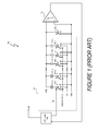
- Successive approximation register (SAR) ADCs represent a popular ADC technology particularly for medium to high resolution ADCs. Although the acronym “SAR” actually stands for Successive Approximation Register (the logic block that controls the conversion process), “SAR” is generally accepted as the acronym for the successive approximation analog-to-digital converter system itself.
- FIG. 1 depicts a general SAR ADC 100 that converts an analog input signal V in into a digital output signal y(n).
- SAR ADC 100 receives the analog input signal V in and employs a digital-to-analog converter (DAC) 101 and a comparator 106 to convert the analog input signal V in into the digital output signal y(n).
- the DAC 101 includes an array of 16 converter reference elements CAP 15 , CAP 14 , . . . , CAP 0 to develop a 16-bit conversion of the analog input signal V in .
- the values of the converter reference elements can be represented by a sixteen element weight vector W with the most significant bit in the initial position.
- the SAR ADC 100 has a resolution equal to one-half of the value of the least significant bit.
- the number of converter reference elements in DAC 101 can be increased or decreased to respectively increase or decrease the resolution of the SAR ADC 100 .
- SAR ADC 100 uses charge redistribution to convert the analog input signal V in into the digital output signal y(n).
- the 16 converter reference elements of CAP 15 , CAP 14 , . . . , CAP 0 are capacitors although other embodiments of SAR ADC 100 can use resistors or other circuit element types.
- the SAR logic 102 generates a successive approximation converter reference element vector C j where j is an updatable index reference.
- SAR ADC 100 begins the conversion process by switching the most significant bit (MSB) switch 104 . 15 to the V in node to charge the most significant bit (MSB) capacitor CAP 15 to a value proportional to a voltage level of the analog input signal V in .
- Switches for the remaining converter reference elements are set by vector C j to connect to the V REF node to charge the remaining converter reference elements to reference voltage V REF , which provides a bipolar offset from the input voltage V in .
- SAR logic 102 next updates the vector C j to change the position of switches 104 . 15 , 104 . 14 , . . . , 104 . 0 and successively move the total trapped charge between each of the converter reference elements in DAC 101 .
- Comparator 106 senses the voltage between the inverting ( ⁇ ) and non-inverting node (+) and provides a binary output that indicates which node has the higher voltage.
- SAR logic 102 initially samples by the analog input signal V in by setting vector C j so that each of switches 104 . 15 , . . . , 104 . 0 , 104 .GND are connected to ground.
- the sampled analog input voltage V in is held by setting vector C j so that element CAP 15 is connected to the reference voltage node V REF and the remaining elements are connected to ground GND.
- Switch 104 .GND is then opened allowing the voltage at the inverting terminal of comparator 106 to move in accordance with the settings of switches 104 . 15 , 104 . 14 , . . . , 104 . 0 . If all switches 104 . 15 , 104 . 14 , . . .
- the voltage at the comparator 106 inputs changes in accordance with the setting of switches 104 . 15 , 104 . 14 , . . . , 104 . 0 .
- the SAR logic 102 detects the voltage output of comparator 106 .
- the SAR logic 102 generates a vector C j and sets each element ⁇ CAP 15 , CAP 14 , . . . , CAP 0 ⁇ of the vector C j based upon the value of the current setting successive approximation converter reference element vector C j and corresponding output of comparator 106 .
- switch 104 . 15 is 1, i.e.
- SAR logic 102 determines each element of the vector C j .
- SAR logic 102 determines the digital value of the analog input signal V in by determining the dot product of an element weight vector W and converting the scalar result into a digital output value digital output signal y(n).
- SAR ADC 100 is configured and operates as described in U.S. Pat. No.
- the weight vector W ⁇ CAP 15 , CAP 14 , . . . , CAP 0 ⁇ .
- the values of CAP 15 , CAP 14 , . . . , CAP 0 can be based upon any radix.
- redundant number systems include binary number systems that include one or more repeating elements, for example ⁇ 1, 1 ⁇ 2, 1 ⁇ 4, 1 ⁇ 8, 1/16, 1/16, 1/32, 1/64, . . . ⁇ .
- the repeating elements are added to generate a desired amount of redundancy.
- the additional elements do not have to be the same.
- a binary sequence with inserted elements that are not power of 2 multiples can be used such as ⁇ 1, 1 ⁇ 2, 1 ⁇ 4, 1 ⁇ 8, 1/16, .75/16, 1/32, 1/64, . . . ⁇ .
- the converter reference elements of DAC 101 are generally fabricated as part of an integrated circuit. Although the values of converter reference elements are designed with specific values, the exact values of CAP 15 , CAP 14 , . . . , CAP 0 are generally unknown.
- a method of calibrating a redundant number system analog-to-digital converter wherein the RNS ADC includes N analog converter reference elements, each of the analog converter reference elements is associated with a weight in a weight vector W , and N is an integer greater than one includes successively approximating each of M distinct analog input signals twice to generate M respective pairs of successive approximation converter reference element vectors, C 1 j and C 2 j , that correspond to digital approximations of the input signals, wherein j ⁇ ⁇ 0, 1, . . . , M-1 ⁇ , wherein M is a positive integer.
- the method further includes using differences between converter reference element vectors of each of the M respective pairs to determine a final weight vector W B .
- a redundant number system, analog-to-digital converter in another embodiment, includes an input to receive an input signal.
- the redundant number system, analog-to-digital converter further includes N analog converter reference elements, coupled to the input, wherein each of the analog converter reference elements is associated with a weight in a weight vector W , and N is an integer greater than one.
- the redundant number system, analog-to-digital converter also includes conversion logic, coupled to the analog converter reference elements, to successively approximate each of M distinct analog input signals twice to generate M respective pairs of successive approximation converter reference element vectors, C 1 j and C 2 j , that correspond to digital approximations of the input signals, wherein j ⁇ ⁇ 0, 1, . . .
- the redundant number system, analog-to-digital converter further includes calibration logic, coupled to the conversion logic to use differences between converter reference element vectors of each of the M respective pairs to determine a final weight vector W B .
- a signal processing system includes a redundant number system successive approximation register (RNS ADC).
- RNS ADC includes a digital-to-analog converter, wherein the digital-to-analog converter includes N analog converter reference elements, each of the analog converter reference elements is represented as a weight in a weight vector W , and N is an integer greater than one.
- the RNS ADC further includes an input to receive a test analog input signal, wherein the analog input signal has a corresponding digital value within a conversion overlap region of the RNS ADC and a comparator, coupled to the input and digital-to-analog converter to generate a comparison signal.
- the RNS ADC also includes conversion logic, coupled to the analog reference signal generator, to receive the comparison signal and to cause the digital-to-analog converter to successively approximate each of M distinct analog input signals twice to generate M respective pairs of successive approximation converter reference element vectors, C 1 j and C 2 j , that correspond to digital approximations of the input signals, wherein j ⁇ ⁇ 0, 1, . . . , M-1 ⁇ , wherein M is a positive integer.
- the RNS ADC further includes calibration logic, coupled to the conversion logic, to use differences between converter reference element vectors of each of the M respective pairs to determine a final weight vector W B .
- an apparatus to calibrate a redundant number system successive approximation register wherein the RNS ADC includes N analog converter reference elements, each of the analog converter reference elements is represented as a weight in a weight vector W , and N is an integer greater than one includes means for successively approximating each of M distinct analog input signals twice to generate M respective pairs of successive approximation converter reference element vectors, C 1 j and C 2 j , that correspond to digital approximations of the input signals, wherein j ⁇ ⁇ 0, 1, . . . , M-1 ⁇ , wherein M is a positive integer.
- the apparatus also includes means for using differences between converter reference element vectors of each of the M respective pairs to determine a final weight vector W B .
- a method of calibrating a redundant number system, analog-to-digital converter includes selecting an input voltage, converting the input voltage into a first conversion, and forcing conversion of the input voltage into a second conversion, wherein the first conversion is different than the second conversion.
- the method also includes calibrating the redundant number system, analog-to-digital converter using the first and second conversions.
- a redundant number system, analog-to-digital converter in another embodiment, includes an input to receive an input voltage and a converter to convert the input voltage into a first conversion and to force conversion of the input voltage into a second conversion, wherein the first conversion is different than the second conversion.
- the converter further includes a calibrator to calibrate the redundant number system, analog-to-digital converter using the first and second conversions.
- FIG. 1 (labeled prior art) depicts a successive approximation register analog to digital converter.
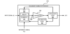
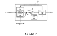
- FIG. 2 depicts a redundant number system analog-to-digital converter having calibration logic for redundant number system converter reference elements.
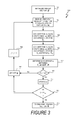
- FIG. 3 depicts an iterative calibration process to determine a final weight vector.
- FIG. 4 depicts conversion overlap regions.
- FIG. 5 depicts a group calibration process to determine a final weight vector.
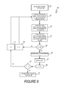
- FIG. 6 depicts a multiple group calibration process to determine a final weight vector.
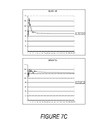
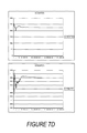
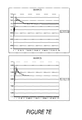
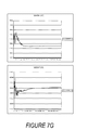
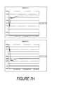
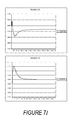
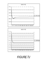
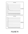
- FIGS. 7A-7K depict convergence of elements in a final weight vector during a calibration process to determine the final weight vector.
- a system and method calibrate a redundant number system analog-to-digital converter (RNS ADC) using successive approximations of multiple input signals and approximating each input signal at least twice.
- the RNS ADC includes N analog converter reference elements, each of the analog converter reference elements is associated with a weight in a weight vector W , and N is an integer greater than one.
- many input signals can correspond to at least two distinct converter reference element conversions.
- Each converter reference element conversion can be represented as a vector.
- the system and method successively approximate each of M distinct analog input signals twice to generate M respective pairs of successive approximation converter reference element vectors, C 1 j and C 2 j , that correspond to digital approximations of the input signals, wherein j ⁇ ⁇ 0, 1, . . . , M-1 ⁇ and M is a positive integer.
- the system and method utilize differences between the successive approximation converter reference element vectors C 1 j and C 2 j to determine a final weight vector W B .
- the difference between C 1 j ⁇ W B and C 2 j ⁇ W B can be used to determine the final weight vector W B .
- the RNS ADC 200 can function like a conventional SAR ADC 100 by multiplying a successive approximation converter reference element vector C j times the final weight vector W B , i.e. C j ⁇ W B , and converting the resultant scalar quantity into the digital output signal y(n). Additionally, the final weight vector W B can be determined to provide the best conversion values, which are not necessarily the actual values of the analog reference elements. Thus, in at least one embodiment the determination of the final weight vector W B can correct for non-ideal values of analog reference elements.
- speed and accuracy represent key RNS ADC calibration concerns.
- RNS ADC is designed to make the fewest possible tests to gather calibration data.
- only those analog input signal values that can cause significantly different conversion pairs should be used.
- the analog input signal values that can cause significantly different conversions are input signal values that can convert to a value in overlap regions.
- coarse calibration does not need the accuracy of fine calibration, so calibration speed optimization can be accomplished, for example, by doing fast initial conversions for a number of cycles, and slower, more accurate, conversions once the calibration has partially converged.
- the fast conversions can be accomplished by, for example, higher clock rate, truncated conversion, or by using the initial capacitor setting in a switched capacitor RNS ADC embodiment as one of the two corresponding conversion data values.
- FIG. 2 depicts a redundant number system analog-to-digital converter 200 that uses successive approximation and RNS calibration logic 202 to determine a calibrated reference element weight vector.
- the analog input signal x(t) to the RNS ADC 200 is an analog signal, and “t” represents a specific time at which the analog input signal x(t) has a specific value.
- the RNS ADC 200 converts the analog input signal x(t) into a digital output signal y(n).
- the RNS ADC 200 includes an input to receive an input voltage.
- the input voltage can be selected so that the input voltage converts to two conversions within a conversion overlap region of a redundant number system.
- the RNS ADC 200 also includes a converter, such as conversion logic 206 , to convert the input voltage into a first conversion and to force conversion of the input voltage into a second conversion, wherein the first conversion is different than the second conversion.
- the RNS ADC 200 also includes a calibrator, such as calibration logic 202 , to calibrate the redundant number system, analog-to-digital converter using the first and second conversions.
- the RNS ADC 200 repeats the process for multiple input signals, for example at least 100 repetitions, and uses the differences between each pair of conversions to determine a final weight vector W B that is used to convert input signals during normal operations of RNS ADC 200 .
- a redundant number system, analog-to-digital converter includes and The converter further includes a calibrator to calibrate the redundant number system, analog-to-digital converter using the first and second conversions.
- RNS ADC 200 is a switched capacitor SAR and, other than during calibration, converts analog input signal x(t) into a digital output signal y(n) in the same manner as SAR ADC 100 .
- the analog converter reference elements 204 of DAC 203 are capacitors.
- the RNS ADC 200 can be configured using any other type of analog converter reference elements, such as resistors, and convert the analog input signal analog input signal x(t) into the digital output signal y(n).
- the number of analog converter reference elements 204 is N, and N is a positive integer and equals, for example, twenty-two.
- the analog converter reference elements 204 implement a redundant number system.
- the values of the analog converter reference elements 204 utilize a redundant number system as described with reference to SAR ADC 100 .
- the analog converter reference elements 204 all have a radix ⁇ 2, duplicate reference element values are used, and/or at least two numerically adjacent weight elements differ by a power factor less than 2.
- RNS ADC 200 is calibrated in accordance with an iterative calibration process 300 .
- each weight w is associated with a value of a capacitor reference element in DAC 203.
- the weight vector W is initialized using the intended design values of each element in the analog converter reference elements 204 . As previously discussed, because of various factors, such as fabrication error and electrical characteristic change over time, the intended values generally do not match the actual values of analog converter reference elements 204 . Additionally, in at least one embodiment the final weight vector W B does not reflect the actual values of analog reference elements 204 but rather is used to obtain the best conversions of analog input signal x(t).
- analog input signal x(t) is received by RNS ADC 200 .
- the values of the analog converter reference elements 204 can be calibrated by converting a single analog input signal x(t) into at least two distinct successive approximation converter reference element vectors C 1 j and C 2 j .
- Vectors C 1 j and C 2 j represent successive approximation converter reference element vectors that correspond to digital approximations of the same, j th sample of the analog input signal x(t).
- j is initialized to zero (0) for the first conversion of analog input signal x(t).
- vectors C 1 j and C 2 j are binary vectors of length N, and C 1 j ⁇ W ⁇ C 2 j ⁇ W .
- the calibration logic 202 can determine a final weight vector W B .
- FIG. 4 depicts a binary redundant number system 400 with multiple conversion overlap regions for a three bit binary sequence.
- the redundant number system used by RNS ADC 200 to successively approximate analog input signal x(t) creates convergence overlap regions, depicted by areas where overlap areas exist.
- the RNS ADC 200 can convert an analog input signal x(t) into two (2) distinct outputs.
- the overlap regions in FIG. 4 can be expanded to cover a number sequence of virtually any length.
- Operation 308 uses comparator 208 to convert the analog input signal x(t) to successive approximation converter reference element vector C 1 j using the analog converter reference elements 204 of DAC 203 .
- Operation 310 uses comparator 208 to convert the same analog input signal x(t) to successive approximation converter reference element vector C 2 j using the analog converter reference elements 204 of DAC 203 .
- calibration logic 202 provides data to conversion logic 206 to ensure that conversion logic 206 converts each analog input signal x(t) twice, and each conversion results in two distinct digital approximations of successive approximation converter reference element vectors C 1 j and C 2 j .
- conversion logic 206 shifts charge within the analog converter reference elements 204 and interprets the output of comparator 208 in the same manner as SAR ADC 100 .
- the vectors C 1 j and C 2 j perform the equivalent function as the vector C j with respect to controlling the state of the switches (not shown) in DAC 203 .
- values for analog input signal x(t) are set by calibration logic 202 that can cause significantly different conversions, i.e. absolute value of [( C 1 j ⁇ W) ⁇ ( C 2 j ⁇ W)] represents a difference that is significant enough so that, in at least one embodiment, the difference converges over time in a relatively short period of time, e.g. less than one second.
- the values of analog input signal x(t) that can cause significantly different conversions are values that can convert to a value in a conversion overlap region of FIG. 4 . Assuming the weight vector W is arranged from large to small analog converter reference elements, i.e.
- calibration logic 202 forces conversion logic 206 to use a logical 1 at position in vector C 1 j and a logical 0 in the same position conversion for vector C 2 j to force vectors C 1 j and C 2 j into conversion overlap regions. If the forced bit is relatively near the most significant bit (“MSB”) location, each element in the weight vector W will converge rapidly, and, in at least one embodiment, a minimum of calibration cycles will be used by iterative calibration process 300 .
- MSB most significant bit
- Table 1 sets forth example digital representations of value patterns for analog input signal x(t) and forced bit selections for successive approximation converter reference element vectors C 1 j and C 2 j that increase the speed of the iterative calibration process 300 .
- the value patterns associated with analog input signal x(t) are for analog reference elements 204 that use a radix of 1.8. Other value patterns are used with other redundant number systems and are constructed to force vectors C 1 j and C 2 j into conversion overlap regions.
- TABLE 1 C 1 j C 2 j ANALOG INPUT SIGNAL x(t) Forced Bits Forced Bits 1 0 0 0 0 R R R . . . 1 . . . 0 . . .
- R R R . . . represents a string of random binary digits.
- bits following the forced bits, as represented by the ellipses, for the successive approximation converter reference element vectors C 1 j and C 2 j represent bits that are determined by operations 308 and 310 using conversion logic 206 in accordance with, for example, the conversion process described in the Melanson Patent.
- the vectors C 1 j and C hd 2 j can be determined using coarse conversions initially followed by finer conversions. So, it is also possible to optimize conversion speed by doing fast initial conversions for a number of cycles, and slower, more accurate, conversion once the calibration has partially converged.
- the fast conversions can be accomplished by, for example, higher clock rate, truncated conversion, or by using the initial cap setting as one of the two data values.
- the calibration processes speed can be increased by not updating the least significant bits of vectors C 1 j and C 2 j at all until the most significant bits of vectors C 1 j and C 2 j have settled down on the coarse adaptation.
- the LSBs can be treated as one “master element” or ensemble. For example, if the relative values of the smaller 8 or so analog converter reference elements 204 are known and adapt them as one element.
- a goal of iterative calibration process 300 is to use the differences between vectors C 1 j and C 2 j of each of the M respective pairs to determine a final weight vector W B .
- operation 312 determines an error e j between C 1 j W and C 2 j ⁇ W .
- W init represents an initial weight vector.
- the values of initial weight vector W hd init are the intended design values of each element in the analog converter reference elements 204 , and initial weight vector W init is normalized in accordance with Equation [1].
- ⁇ is a gain. In at least one embodiment, the gain ⁇ increases a rate of convergence of the error e i to within the predetermined thresholds.
- ⁇ is a vector ⁇
- element values of the vector ⁇ have a decreasing step size so that an element modifying a more significant bit of ( C 1 j ⁇ C 2 j ) is larger than an element modifying a lesser significant bit.
- Operation 320 updates the index j by one.
- Operation 304 then receives a new analog input signal x(t) that is preferably set by calibration logic 202 as previously described so that successive approximation converter reference element vectors C 1 j and C 2 j are within a conversion overlap region.
- Operation 314 determines an error E.
- the error E is based on the previous individual errors e j .
- the error E represents a square of a running average of e j for all j ⁇ M.
- Operation 315 determines whether the error E is less than or equal to a maximum threshold value TH max .
- the error E is a function of previous errors e j for all j ⁇ M.
- the threshold value TH max is a matter of design choice and represents a desired accuracy between the determined final weight vector W B and the actual value of the analog converter reference elements 204 .
- M is also a matter of design choice and can be determined, for example, by simulating RNS ADC 200 to determine a number of cycles of iterative calibration process 300 needed so that the error e j converges below the threshold value TH max .
- M equals 100.
- operation 315 determines that the error E is less than or equal to TH max , then operation 316 stores the last weight vector determined by operation 318 as the final weight vector W B . However, if E is outside of the threshold values, operations 318 , 320 , and 304 - 315 continue until E is less than or equal to TH max .
- ⁇ is a vector ⁇
- element values of the vector ⁇ have a decreasing step size so that an element modifying a more significant bit of ( C 1 j ⁇ C 2 j ) is larger than an element modifying a lesser significant bit.
- FIG. 5 depicts group calibration process 500 .
- RNS ADC 200 is calibrated in accordance with group calibration process 500 .
- the iterative calibration process 300 updates the weight vector during each cycle of iterative calibration process 300 and, thus, utilizes a minimum amount of memory because it is unnecessary to store each of the vectors C 1 j and C 2 j for all j.
- Group calibration process 500 uses the differences between converter reference element vectors C 1 j and C 2 j of each of M respective pairs of vectors C 1 j and C 2 j to determine a final weight vector W B directly without the iteration of iterative calibration process 300 .
- the group calibration process 500 requires more memory than iterative calibration process 300 but is generally faster and more accurate.
- operations 304 - 310 of group calibration process 500 are identical to the same operations in iterative calibration process 300 .
- Operation 502 determines if j equals M. If j does not equal M, then group calibration process 500 repeats operations 304 - 310 after updating the index j in operation 504 and returning to operation 304 . Once operation 502 determines that j equals M, group calibration process 500 has determined M pairs of vectors C 1 j and C 2 j
- Operation 506 determines a final weight vector W B using the differences between pairs of vectors C 1 j and C 2 j .
- group calibration process 500 performs additional conversions and after each additional conversion determines the group minimum error e min using Equation [7], with M equaling the number of cycles through operations 304 - 310 , until the conditions of Equation [8] are met.
- FIG. 6 depicts multiple group calibration process 600 .
- RNS ADC 200 is calibrated in accordance with multiple group calibration process 600 .
- Group calibration process 600 uses the differences between vectors C 1 j and C 2 j from Y-1 multiple groups of M i respective pairs of vectors C 1 j and C 2 j to determine a final weight vector W B , where M i and Y are respective integers greater than one.
- the multiple group calibration process 600 represents a hybrid calibration process between iterative calibration process 300 and group calibration process 500 .
- the multiple group calibration process 600 requires more memory than iterative calibration process 300 but less memory than group calibration process 500 .
- the performance and accuracy of multiple group calibration process 600 generally lies between the performance and accuracies of iterative calibration process 300 and group calibration process 500 .
- operations 302 - 310 of multiple group calibration process 600 are identical to the same operations in iterative calibration process 300 .
- the initial operation 606 updates the weight vector W 0 in accordance with Equation [13]:
- Operation 608 updates the group index i by one, and operation 610 determines whether all Y-1 groups have been processed. If all Y-1 groups have not been processed, operation 611 resets the index j to 0, and multiple group calibration process 600 cycles.
- Operation 606 updates the weight vector W i in accordance with Equation [15]:
- W _ i W _ i - 1 - 1 ( B - A + 1 )
- ⁇ ⁇ j A B ⁇ ⁇ [ ( C _ 1 j - C _ 2 j ) ⁇ e i ⁇ ⁇ ] .
- W init is the normalized, initial weight vector and ⁇ is a gain.
- ⁇ is a vector ⁇
- operation 612 stores W Y-1 as the final weight vector W B .
- the RNS ADC 200 can function like a conventional SAR ADC 100 by multiplying a successive approximation converter reference element vector C j times the final weight vector W B , i.e. C j ⁇ W B , and converting the resultant scalar quantity into the digital output signal digital output signal y(n).
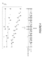
- FIGS. 7A through 7K illustrate the convergence of elements 0 through 21 of a 22 element weight vector W during calibration.
- Mathematica® computer program that simulates the operation of at least one embodiment of the RNS ADC 200 and demonstrates an algorithm that generates weights in accordance with at least one embodiment of group calibration process 500 , for the simulated operation of RNS ADC 200 .
- the computer program can be used with Mathematica® software, available from Wolfram Research, Inc. having an office in Champaign, Ill., or with Mathematica® compatible software programs such as MathReader or Publicon.:
- the value of the gain ⁇ can be adaptively changed, faster when large, more accurate when small.
Abstract
Description
- This application claims the benefit under 35 U.S.C. §119(e) of U.S. Provisional Application No. 60/722,275, filed Sep. 30, 2005 and entitled “Calibration of Redundant Number Systems SAR Converter.” U.S. Provisional Application No. 60/722,275 includes exemplary systems and methods and is incorporated by reference in its entirety.
- 1. Field of the Invention
- The present invention relates in general to the field of signal processing, and more specifically, to a system and method for calibrating a redundant number system successive approximation analog-to-digital converter.
- 2. Description of the Related Art
- Analog-to-digital converters (ADCs) convert analog signals into digital signals. ADCs find widespread use in many mixed signal applications. Converting analog audio signals into digital signals represents a common mixed signal application. Successive approximation register (SAR) ADCs represent a popular ADC technology particularly for medium to high resolution ADCs. Although the acronym “SAR” actually stands for Successive Approximation Register (the logic block that controls the conversion process), “SAR” is generally accepted as the acronym for the successive approximation analog-to-digital converter system itself.
-
FIG. 1 depicts ageneral SAR ADC 100 that converts an analog input signal Vin into a digital output signal y(n). In general, SAR ADC 100 receives the analog input signal Vin and employs a digital-to-analog converter (DAC) 101 and acomparator 106 to convert the analog input signal Vin into the digital output signal y(n). TheDAC 101 includes an array of 16 converter reference elements CAP15, CAP14, . . . , CAP0 to develop a 16-bit conversion of the analog input signal Vin. The values of the converter reference elements can be represented by a sixteen element weight vectorW with the most significant bit in the initial position. The SAR ADC 100 has a resolution equal to one-half of the value of the least significant bit. The number of converter reference elements inDAC 101 can be increased or decreased to respectively increase or decrease the resolution of theSAR ADC 100. - SAR ADC 100 uses charge redistribution to convert the analog input signal Vin into the digital output signal y(n). The 16 converter reference elements of CAP15, CAP14, . . . , CAP0 are capacitors although other embodiments of SAR ADC 100 can use resistors or other circuit element types. The
SAR logic 102 generates a successive approximation converter reference element vectorC j where j is an updatable index reference. The values of vectorC j, {CAP15, CAP14, . . . , CAP0}, control the position of switches 104.15, 104.14, . . . , 104.0, 104.GND. SARADC 100 begins the conversion process by switching the most significant bit (MSB) switch 104.15 to the Vin node to charge the most significant bit (MSB) capacitor CAP15 to a value proportional to a voltage level of the analog input signal Vin. Switches for the remaining converter reference elements are set by vectorC j to connect to the VREF node to charge the remaining converter reference elements to reference voltage VREF, which provides a bipolar offset from the input voltage Vin. SAR logic 102 next updates the vectorC j to change the position of switches 104.15, 104.14, . . . , 104.0 and successively move the total trapped charge between each of the converter reference elements inDAC 101.Comparator 106 senses the voltage between the inverting (−) and non-inverting node (+) and provides a binary output that indicates which node has the higher voltage. -
SAR logic 102 initially samples by the analog input signal Vin by setting vectorC j so that each of switches 104.15, . . . , 104.0, 104.GND are connected to ground. The sampled analog input voltage Vin is held by setting vectorC j so that element CAP15 is connected to the reference voltage node VREF and the remaining elements are connected to ground GND. Switch 104.GND is then opened allowing the voltage at the inverting terminal ofcomparator 106 to move in accordance with the settings of switches 104.15, 104.14, . . . , 104.0. If all switches 104.15, 104.14, . . . , 104.0 are connected to the ground node GND, a voltage equal to −Vin appears at the inverting terminal ofcomparator 106. With CAP15 connected to ground, a voltage equal to voltage VREF divided by the ratio of the value of element CAP15 to the total of all values of the capacitors in the converter reference element array ofDAC 101. If the output of comparator is a logical 1,SAR logic 102 latches switch 104.15 to the reference voltage node VREF; otherwiseSAR logic 102 latches switch 104.15 to the ground node GND. The process continues until theSAR logic 102 has cycled and set each of the switches 104.15, 104.14, . . . , 104.0. - Thus, during each move of the total trapped charge, the voltage at the
comparator 106 inputs changes in accordance with the setting of switches 104.15, 104.14, . . . , 104.0. TheSAR logic 102 detects the voltage output ofcomparator 106. TheSAR logic 102 generates a vectorC j and sets each element {CAP15, CAP14, . . . , CAP0} of the vectorC j based upon the value of the current setting successive approximation converter reference element vectorC j and corresponding output ofcomparator 106. Thus, if switch 104.15 is 1, i.e. connected to voltage reference node VREF, and the output ofcomparator 106 is logical 1, then CAP15 is 1. In the next iteration, if switch 104.14 is then 1 and the output ofcomparator 106 is logical 0, then CAP14 is 0, and so on untilSAR logic 102 determines each element of the vectorC j.SAR logic 102 determines the digital value of the analog input signal Vin by determining the dot product of an element weight vectorW and converting the scalar result into a digital output value digital output signal y(n). In at least one embodiment, SAR ADC 100 is configured and operates as described in U.S. Pat. No. 6,844840, “Successive-Approximation-Register (SAR) Analog-To-Digital Converter (ADC) and Method Utilizing N Three-Way Elements”, inventor John L. Melanson, assigned to Cirrus Logic, Inc., and issued Jun. 18, 2005, referred to herein as “Melanson Patent”. The Melanson Patent is hereby incorporated by reference in its entirety. - The weight vector
W ={CAP15, CAP14, . . . , CAP0}. The values of CAP15, CAP14, . . . , CAP0 can be based upon any radix. In one embodiment, a radix of 2 is used so that the weight vectorW ={CAP15, CAP15/(21), CAP15/(22), . . . , CAP15/(215)}. In other embodiments, a radix of less than 2 is used, such as a radix equal to 1.8 so that the weight vectorW ={CAP15, CAP15/(1.81), CAP15/(1.82), . . . , CAP15/(1.815)}. Other redundant number systems include binary number systems that include one or more repeating elements, for example {1, ½, ¼, ⅛, 1/16, 1/16, 1/32, 1/64, . . . }. The repeating elements are added to generate a desired amount of redundancy. In another embodiment, the additional elements do not have to be the same. For example, a binary sequence with inserted elements that are not power of 2 multiples can be used such as {1, ½, ¼, ⅛, 1/16, .75/16, 1/32, 1/64, . . . }. - As described in exemplary embodiments of U.S. Pat. No. 4,336,526, using a radix of less than two provides one embodiment of a redundant number system. Using a redundant number system provides overlap in the conversion process of
SAR logic 102, thus, allowing for imprecision in the fabrication of the actual converter reference elements inDAC 101. U.S. Pat. No. 4,336,526, entitled “Successive Approximation Analog-to-Digital Converter Using Non-Binary Series”, inventor Basil Weir, and issued on Jun. 22, 1982, is hereby incorporated by reference in its entirety. - The converter reference elements of
DAC 101 are generally fabricated as part of an integrated circuit. Although the values of converter reference elements are designed with specific values, the exact values of CAP15, CAP14, . . . , CAP0 are generally unknown. - In one embodiment of the present invention, a method of calibrating a redundant number system analog-to-digital converter (RNS ADC), wherein the RNS ADC includes N analog converter reference elements, each of the analog converter reference elements is associated with a weight in a weight vector
W , and N is an integer greater than one includes successively approximating each of M distinct analog input signals twice to generate M respective pairs of successive approximation converter reference element vectors,C 1j andC 2j , that correspond to digital approximations of the input signals, wherein j ε {0, 1, . . . , M-1}, wherein M is a positive integer. The method further includes using differences between converter reference element vectors of each of the M respective pairs to determine a final weight vectorW B. - In another embodiment of the present invention, a redundant number system, analog-to-digital converter includes an input to receive an input signal. The redundant number system, analog-to-digital converter further includes N analog converter reference elements, coupled to the input, wherein each of the analog converter reference elements is associated with a weight in a weight vector
W , and N is an integer greater than one. The redundant number system, analog-to-digital converter also includes conversion logic, coupled to the analog converter reference elements, to successively approximate each of M distinct analog input signals twice to generate M respective pairs of successive approximation converter reference element vectors,C 1j andC 2j , that correspond to digital approximations of the input signals, wherein j ε {0, 1, . . . , M-1}, wherein M is a positive integer. The redundant number system, analog-to-digital converter further includes calibration logic, coupled to the conversion logic to use differences between converter reference element vectors of each of the M respective pairs to determine a final weight vectorW B. - In a further embodiment of the present invention, a signal processing system includes a redundant number system successive approximation register (RNS ADC). the RNS ADC includes a digital-to-analog converter, wherein the digital-to-analog converter includes N analog converter reference elements, each of the analog converter reference elements is represented as a weight in a weight vector
W , and N is an integer greater than one. The RNS ADC further includes an input to receive a test analog input signal, wherein the analog input signal has a corresponding digital value within a conversion overlap region of the RNS ADC and a comparator, coupled to the input and digital-to-analog converter to generate a comparison signal. The RNS ADC also includes conversion logic, coupled to the analog reference signal generator, to receive the comparison signal and to cause the digital-to-analog converter to successively approximate each of M distinct analog input signals twice to generate M respective pairs of successive approximation converter reference element vectors,C 1j andC 2j , that correspond to digital approximations of the input signals, wherein j ε {0, 1, . . . , M-1}, wherein M is a positive integer. The RNS ADC further includes calibration logic, coupled to the conversion logic, to use differences between converter reference element vectors of each of the M respective pairs to determine a final weight vectorW B. - In another embodiment of the present invention, an apparatus to calibrate a redundant number system successive approximation register (RNS ADC), wherein the RNS ADC includes N analog converter reference elements, each of the analog converter reference elements is represented as a weight in a weight vector
W , and N is an integer greater than one includes means for successively approximating each of M distinct analog input signals twice to generate M respective pairs of successive approximation converter reference element vectors,C 1j andC 2j , that correspond to digital approximations of the input signals, wherein j ε {0, 1, . . . , M-1}, wherein M is a positive integer. The apparatus also includes means for using differences between converter reference element vectors of each of the M respective pairs to determine a final weight vectorW B. - In a further embodiment of the invention, a method of calibrating a redundant number system, analog-to-digital converter includes selecting an input voltage, converting the input voltage into a first conversion, and forcing conversion of the input voltage into a second conversion, wherein the first conversion is different than the second conversion. The method also includes calibrating the redundant number system, analog-to-digital converter using the first and second conversions.
- In another embodiment of the present invention, a redundant number system, analog-to-digital converter includes an input to receive an input voltage and a converter to convert the input voltage into a first conversion and to force conversion of the input voltage into a second conversion, wherein the first conversion is different than the second conversion. The converter further includes a calibrator to calibrate the redundant number system, analog-to-digital converter using the first and second conversions.
- The present invention may be better understood, and its numerous objects, features and advantages made apparent to those skilled in the art by referencing the accompanying drawings. The use of the same reference number throughout the several figures designates a like or similar element.
-
FIG. 1 (labeled prior art) depicts a successive approximation register analog to digital converter. -
FIG. 2 depicts a redundant number system analog-to-digital converter having calibration logic for redundant number system converter reference elements. -
FIG. 3 depicts an iterative calibration process to determine a final weight vector. -
FIG. 4 depicts conversion overlap regions. -
FIG. 5 depicts a group calibration process to determine a final weight vector. -
FIG. 6 depicts a multiple group calibration process to determine a final weight vector. -
FIGS. 7A-7K depict convergence of elements in a final weight vector during a calibration process to determine the final weight vector. - A system and method calibrate a redundant number system analog-to-digital converter (RNS ADC) using successive approximations of multiple input signals and approximating each input signal at least twice. The RNS ADC includes N analog converter reference elements, each of the analog converter reference elements is associated with a weight in a weight vector
W , and N is an integer greater than one. In a redundant number system, many input signals can correspond to at least two distinct converter reference element conversions. Each converter reference element conversion can be represented as a vector. The system and method successively approximate each of M distinct analog input signals twice to generate M respective pairs of successive approximation converter reference element vectors,C 1j andC 2j , that correspond to digital approximations of the input signals, wherein j ε {0, 1, . . . , M-1} and M is a positive integer. The system and method utilize differences between the successive approximation converter reference element vectorsC 1j andC 2j to determine a final weight vectorW B. Thus, in at least one embodiment, the difference betweenC 1j ·W B andC 2j ·W B can be used to determine the final weight vectorW B. Once a final weight vectorW B is determined through one of the calibration processes described herein, theRNS ADC 200 can function like aconventional SAR ADC 100 by multiplying a successive approximation converter reference element vectorC j times the final weight vectorW B, i.e.C j·W B, and converting the resultant scalar quantity into the digital output signal y(n). Additionally, the final weight vectorW B can be determined to provide the best conversion values, which are not necessarily the actual values of the analog reference elements. Thus, in at least one embodiment the determination of the final weight vectorW B can correct for non-ideal values of analog reference elements. - In at least one embodiment, speed and accuracy represent key RNS ADC calibration concerns. In at least one embodiment, RNS ADC is designed to make the fewest possible tests to gather calibration data. In at least one embodiment, only those analog input signal values that can cause significantly different conversion pairs should be used. In at least one embodiment, the analog input signal values that can cause significantly different conversions are input signal values that can convert to a value in overlap regions. Also, coarse calibration does not need the accuracy of fine calibration, so calibration speed optimization can be accomplished, for example, by doing fast initial conversions for a number of cycles, and slower, more accurate, conversions once the calibration has partially converged. The fast conversions can be accomplished by, for example, higher clock rate, truncated conversion, or by using the initial capacitor setting in a switched capacitor RNS ADC embodiment as one of the two corresponding conversion data values.
-
FIG. 2 depicts a redundant number system analog-to-digital converter 200 that uses successive approximation andRNS calibration logic 202 to determine a calibrated reference element weight vector. The analog input signal x(t) to theRNS ADC 200 is an analog signal, and “t” represents a specific time at which the analog input signal x(t) has a specific value. TheRNS ADC 200 converts the analog input signal x(t) into a digital output signal y(n). - In general the
RNS ADC 200 includes an input to receive an input voltage. The input voltage can be selected so that the input voltage converts to two conversions within a conversion overlap region of a redundant number system. TheRNS ADC 200 also includes a converter, such asconversion logic 206, to convert the input voltage into a first conversion and to force conversion of the input voltage into a second conversion, wherein the first conversion is different than the second conversion. TheRNS ADC 200 also includes a calibrator, such ascalibration logic 202, to calibrate the redundant number system, analog-to-digital converter using the first and second conversions. In at least one embodiment, theRNS ADC 200 repeats the process for multiple input signals, for example at least 100 repetitions, and uses the differences between each pair of conversions to determine a final weight vectorW B that is used to convert input signals during normal operations ofRNS ADC 200. - In another embodiment of the present invention, a redundant number system, analog-to-digital converter includes and The converter further includes a calibrator to calibrate the redundant number system, analog-to-digital converter using the first and second conversions.
- In at least one embodiment,
RNS ADC 200 is a switched capacitor SAR and, other than during calibration, converts analog input signal x(t) into a digital output signal y(n) in the same manner asSAR ADC 100. In a switched capacitor configuration, the analogconverter reference elements 204 ofDAC 203 are capacitors. TheRNS ADC 200 can be configured using any other type of analog converter reference elements, such as resistors, and convert the analog input signal analog input signal x(t) into the digital output signal y(n). In at least one embodiment, the number of analogconverter reference elements 204 is N, and N is a positive integer and equals, for example, twenty-two. The analogconverter reference elements 204 implement a redundant number system. In at least one embodiment, the values of the analogconverter reference elements 204 utilize a redundant number system as described with reference toSAR ADC 100. For example, in at least one embodiment, the analogconverter reference elements 204 all have a radix <2, duplicate reference element values are used, and/or at least two numerically adjacent weight elements differ by a power factor less than 2. - Referring to
FIGS. 2 and 3 , in at least one embodiment,RNS ADC 200 is calibrated in accordance with aniterative calibration process 300.Operation 302 initializes weight vectorW , whereW ={w0, w1, . . . , wN-1} and w0 represents the most significant bit element of the analogconverter reference elements 204, w1 represents the next most significant bit element (i.e. the largest) of the analogconverter reference elements 204, and so on, with wN-1 representing the least significant bit element (i.e. the smallest) of the analogconverter reference elements 204. In a switched capacitor implementation ofRNS ADC 200, each weight w is associated with a value of a capacitor reference element inDAC 203. In at least one embodiment, the weight vectorW is initialized using the intended design values of each element in the analogconverter reference elements 204. As previously discussed, because of various factors, such as fabrication error and electrical characteristic change over time, the intended values generally do not match the actual values of analogconverter reference elements 204. Additionally, in at least one embodiment the final weight vectorW B does not reflect the actual values ofanalog reference elements 204 but rather is used to obtain the best conversions of analog input signal x(t). In at least one embodiment, weight vectorW is normalized to set a largest weight, w0, equal to a fixed value and all remaining weights to a fraction of the largest weight so that the sum of all weights wi is equals one for all i={0, 1, . . . , N-1}, i.e. - Referring to
FIGS. 2, 3 , and 4, inoperation 304, analog input signal x(t) is received byRNS ADC 200. The values of the analogconverter reference elements 204 can be calibrated by converting a single analog input signal x(t) into at least two distinct successive approximation converter reference element vectorsC 1j andC 2j . VectorsC 1j andC 2j represent successive approximation converter reference element vectors that correspond to digital approximations of the same, jth sample of the analog input signal x(t). In at least one embodiment, j is initialized to zero (0) for the first conversion of analog input signal x(t). Also, in at least one embodiment, vectorsC 1j andC 2j are binary vectors of length N, andC 1j ·W ˜C 2j ·W . Given a sufficient number, e.g. at least 100, of near identities ofC 1j ·W ˜C 2j ·W , thecalibration logic 202 can determine a final weight vectorW B . - The most useful information in calibrating the
RNS ADC 200 occurs when the successive approximation converter reference element vectorsC 1j andC 2j are determined from an analog input signal x(t) having a magnitude that causes different conversions of analog input signal x(t) within ‘conversion overlap regions’. In at least one embodiment, the greater the difference between vectorsC 1j andC 2j , the more useful the difference is in determining a final weight vectorW B.FIG. 4 depicts a binaryredundant number system 400 with multiple conversion overlap regions for a three bit binary sequence. The redundant number system used byRNS ADC 200 to successively approximate analog input signal x(t) creates convergence overlap regions, depicted by areas where overlap areas exist. In a conversion overlap region, theRNS ADC 200 can convert an analog input signal x(t) into two (2) distinct outputs. The overlap regions inFIG. 4 can be expanded to cover a number sequence of virtually any length. -
Operation 308 usescomparator 208 to convert the analog input signal x(t) to successive approximation converter reference element vectorC 1j using the analogconverter reference elements 204 ofDAC 203.Operation 310 usescomparator 208 to convert the same analog input signal x(t) to successive approximation converter reference element vectorC 2j using the analogconverter reference elements 204 ofDAC 203. Inoperations calibration logic 202 provides data toconversion logic 206 to ensure thatconversion logic 206 converts each analog input signal x(t) twice, and each conversion results in two distinct digital approximations of successive approximation converter reference element vectorsC 1j andC 2j . In at least one embodiment,conversion logic 206 shifts charge within the analogconverter reference elements 204 and interprets the output ofcomparator 208 in the same manner asSAR ADC 100. In at least one embodiment, the vectorsC 1j andC 2j perform the equivalent function as the vectorC j with respect to controlling the state of the switches (not shown) inDAC 203. - For fast convergence, values for analog input signal x(t) are set by
calibration logic 202 that can cause significantly different conversions, i.e. absolute value of [(C 1j ·W)−(C 2j ·W)] represents a difference that is significant enough so that, in at least one embodiment, the difference converges over time in a relatively short period of time, e.g. less than one second. As previously stated, the values of analog input signal x(t) that can cause significantly different conversions are values that can convert to a value in a conversion overlap region ofFIG. 4 . Assuming the weight vectorW is arranged from large to small analog converter reference elements, i.e. left to right within vectorW , digital value equivalents of analog input signal x(t) values of the following form are good because the analog input signal x(t) value can be converted using vectorsC 1j andC 2j with either a leading 1 or 0 such that vectorsC 1j andC 2j are of the form:
X X X X X R R R R R R . . .
Each “X” is a forced 0 or 1 to force the analog input signal x(t) to convert into a successive approximation converter reference element vector within a conversion overlap region. “R R R . . . ” represents a string of random binary digits determined using a conventional successive approximation process. In at least one embodiment,calibration logic 202forces conversion logic 206 to use a logical 1 at position in vectorC 1j and a logical 0 in the same position conversion for vectorC 2j to force vectorsC 1j andC 2j into conversion overlap regions. If the forced bit is relatively near the most significant bit (“MSB”) location, each element in the weight vectorW will converge rapidly, and, in at least one embodiment, a minimum of calibration cycles will be used byiterative calibration process 300. - Table 1 sets forth example digital representations of value patterns for analog input signal x(t) and forced bit selections for successive approximation converter reference element vectors
C 1j andC 2j that increase the speed of theiterative calibration process 300. The value patterns associated with analog input signal x(t) are foranalog reference elements 204 that use a radix of 1.8. Other value patterns are used with other redundant number systems and are constructed to force vectorsC 1j andC 2j into conversion overlap regions.TABLE 1 C 1j C 2j ANALOG INPUT SIGNAL x(t) Forced Bits Forced Bits 1 0 0 0 0 R R R . . . 1 . . . 0 . . . 0 1 1 1 1 R R R . . . 1 . . . 0 . . . 1 1 0 0 0 0 R R R . . . 1 1 . . . 1 0 . . . 0 0 1 1 1 1 R R R . . . 0 1 . . . 0 0 . . . 1 1 1 0 0 0 0 R R R . . . 1 1 1 . . . 1 1 0 . . . 0 0 0 1 1 1 1 R R R . . . 0 0 1 . . . 0 0 0 . . . 1 0 1 0 0 0 0 R R R . . . 1 0 1 . . . 1 0 0 . . . 0 1 0 1 1 1 1 R R R . . . 0 1 1 . . . 0 1 0 . . . . . . . . . . . .
In Table 1, “R R R . . . ” represents a string of random binary digits. The bits following the forced bits, as represented by the ellipses, for the successive approximation converter reference element vectorsC 1j andC 2j represent bits that are determined byoperations conversion logic 206 in accordance with, for example, the conversion process described in the Melanson Patent. - In at least one embodiment applicable to all the calibration processes described herein, the vectors
C 1j andC hd 2j can be determined using coarse conversions initially followed by finer conversions. So, it is also possible to optimize conversion speed by doing fast initial conversions for a number of cycles, and slower, more accurate, conversion once the calibration has partially converged. The fast conversions can be accomplished by, for example, higher clock rate, truncated conversion, or by using the initial cap setting as one of the two data values. In at least one embodiment, the calibration processes speed can be increased by not updating the least significant bits of vectorsC 1j andC 2j at all until the most significant bits of vectorsC 1j andC 2j have settled down on the coarse adaptation. In at least one embodiment applicable to all the calibration processes described herein, the LSBs can be treated as one “master element” or ensemble. For example, if the relative values of the smaller 8 or so analogconverter reference elements 204 are known and adapt them as one element. - In at least one embodiment, a goal of
iterative calibration process 300 is to use the differences between vectorsC 1j andC 2j of each of the M respective pairs to determine a final weight vectorW B. - During each cycle of
iterative calibration process 300,operation 312 determines an error ej betweenC 1j W andC 2j ·W . The first error e0 is determined from Equation [2] and:
e 0=[(C 10 −C 20 )·W init]2 [2].
W init represents an initial weight vector. In at least one embodiment, the values of initial weight vectorW hd init are the intended design values of each element in the analogconverter reference elements 204, and initial weight vectorW init is normalized in accordance with Equation [1]. -
Operation 313 ensures that theiterative calibration process 300 cycles at least M times so that a sufficient number of errors have been determined to provide a meaningful evaluation of ej. Ifoperation 313 determines that j<M, then the weight vectorW is updated in accordance with Equation [3] using a least mean square process:
W 0 =W init−(C 10 −C 20 )·e 0·μ [3].
where μ is a gain. In at least one embodiment, the gain μ increases a rate of convergence of the error ei to within the predetermined thresholds. In at least one embodiment, μ is a vectorμ , and element values of the vectorμ have a decreasing step size so that an element modifying a more significant bit of (C 1j −C 2j ) is larger than an element modifying a lesser significant bit.Operation 320 updates the index j by one.Operation 304 then receives a new analog input signal x(t) that is preferably set bycalibration logic 202 as previously described so that successive approximation converter reference element vectorsC 1j andC 2j are within a conversion overlap region. - During subsequent cycles of
iterative calibration process 300,operation 312 updates the error in accordance with Equation [4]:
e i=[(C 1i −C 2i )·W i]2 [4].
Operation 318 updates the weight vectorW in accordance with Equation [5]:
W i =W i-1−(C 1i −C 2i )·e i·μ [5]. - Over M cycles of
iterative calibration process 300, the absolute value of the error ej will generally oscillate and eventually converge towards a smaller threshold value THmax.Operation 314 determines an error E. The error E is based on the previous individual errors ej. In at least one embodiment, the error E represents a square of a running average of ej for all j≧M. Operation 315 determines whether the error E is less than or equal to a maximum threshold value THmax. The error E is a function of previous errors ej for all j≧M. The threshold value THmax is a matter of design choice and represents a desired accuracy between the determined final weight vectorW B and the actual value of the analogconverter reference elements 204. The value of M is also a matter of design choice and can be determined, for example, by simulatingRNS ADC 200 to determine a number of cycles ofiterative calibration process 300 needed so that the error ej converges below the threshold value THmax. In at least one embodiment, M equals 100. - If
operation 315 determines that the error E is less than or equal to THmax, thenoperation 316 stores the last weight vector determined byoperation 318 as the final weight vectorW B . However, if E is outside of the threshold values,operations operation 318 uses a least mean square process to determineW 0 in accordance with Equation [6]:
W 0 =W init−(C 10 −C 20 )·e 0·μ [6]
where μ is a gain. In at least one embodiment, μ is a vectorμ , and element values of the vectorμ have a decreasing step size so that an element modifying a more significant bit of (C 1j −C 2j ) is larger than an element modifying a lesser significant bit. - In another embodiment,
operation 314 is not used, and whenoperation 313 determines that j=M,iterative calibration process 300 proceeds directly tooperation 316 after cycling through operations 304-313 and 320 M times. -
FIG. 5 depictsgroup calibration process 500. Referring toFIGS. 2 and 5 , in at least one embodiment,RNS ADC 200 is calibrated in accordance withgroup calibration process 500. Theiterative calibration process 300 updates the weight vector during each cycle ofiterative calibration process 300 and, thus, utilizes a minimum amount of memory because it is unnecessary to store each of the vectorsC 1j andC 2j for all j.Group calibration process 500 uses the differences between converter reference element vectorsC 1j andC 2j of each of M respective pairs of vectorsC 1j andC 2j to determine a final weight vectorW B directly without the iteration ofiterative calibration process 300. Thegroup calibration process 500 requires more memory thaniterative calibration process 300 but is generally faster and more accurate. - In at least one embodiment, operations 304-310 of
group calibration process 500 are identical to the same operations initerative calibration process 300.Operation 502 determines if j equals M. If j does not equal M, thengroup calibration process 500 repeats operations 304-310 after updating the index j inoperation 504 and returning tooperation 304. Onceoperation 502 determines that j equals M,group calibration process 500 has determined M pairs of vectorsC 1j andC 2j -
Operation 506 then determines a final weight vectorW B using the differences between pairs of vectorsC 1j andC 2j . Inoperation 506, the vectorsC 1j andC 2j can be, for example, organized into a matrix and processed to find the final weight vectorW B that minimizes: - In at least one embodiment, the value of M is predetermined to be large enough so that the group minimum error emin is less than or equal to a predetermined threshold TH in accordance with Equation [8]:
Operation 508 stores the final weight vectorW B. - In at least one other embodiment, if the conditions of Equation [8] are not met,
group calibration process 500 performs additional conversions and after each additional conversion determines the group minimum error emin using Equation [7], with M equaling the number of cycles through operations 304-310, until the conditions of Equation [8] are met. Thus,group calibration process 500 uses the differences between vectorsC 1j andC 2j of each of the M respective pairs to determine a final weight vectorW B such that in at least one embodiment: -
FIG. 6 depicts multiplegroup calibration process 600. Referring toFIGS. 2 and 6 , in at least one embodiment,RNS ADC 200 is calibrated in accordance with multiplegroup calibration process 600.Group calibration process 600 uses the differences between vectorsC 1j andC 2j from Y-1 multiple groups of Mi respective pairs of vectorsC 1 j andC 2j to determine a final weight vectorW B, where Mi and Y are respective integers greater than one. - The multiple
group calibration process 600 represents a hybrid calibration process betweeniterative calibration process 300 andgroup calibration process 500. The multiplegroup calibration process 600 requires more memory thaniterative calibration process 300 but less memory thangroup calibration process 500. The performance and accuracy of multiplegroup calibration process 600 generally lies between the performance and accuracies ofiterative calibration process 300 andgroup calibration process 500. - In at least one embodiment, the goal of multiple
group calibration process 600 is to determine a final weight vectorW B using Y iteratively determined weight vectors from respective groups of Mi pairs of vectorsC 1j andC 2j , such that weight vectorW 0 for a first group (i=0) is determined so that:
for all i={ 1, 2, . . . , Y-1} and using weight vectorW i-1 to determine each subsequent group weight vectorW i so that:
wherein
each represent a number of pairs of distinct conversions, Y represents a number of groups of pairs of distinct conversions, Y is an integer greater than
each THi for all i={0, 1, 2, . . . , Y-1} is a respective threshold value, and i is an integer greater than zero. - In at least one embodiment, operations 302-310 of multiple
group calibration process 600 are identical to the same operations initerative calibration process 300.Operation 602 determines whether j=Mi, which determines whether Mi pairs of successive approximation converter reference element vectorsC 1j andC 2j have been determined, where Mi represents the number of pairs of vectorsC 1j andC 2j in the ith group. If not,operation 604 updates the index j by 1 and operations 304-602 repeat until j=Mi. Once j=Mi, for the first group, M0,operation 604 determines an initial group error e0 in accordance with Equation [12]:
whereW init is the normalized, initial weight vector. - The
initial operation 606 updates the weight vectorW 0 in accordance with Equation [13]: -
Operation 608 updates the group index i by one, andoperation 610 determines whether all Y-1 groups have been processed. If all Y-1 groups have not been processed,operation 611 resets the index j to 0, and multiplegroup calibration process 600 cycles. During each subsequent cycle of multiplegroup calibration process 600, whenoperation 602 determines that j=M,operation 604 determines the ith group error ei in accordance with Equation [14]:
Operation 606 updates the weight vectorW i in accordance with Equation [15]:
W init is the normalized, initial weight vector and μ is a gain. In at least one embodiment, μ is a vectorμ , and element values of the vectorμ have a decreasing step size so that an element modifying a more significant bit of
is larger than an element modifying a lesser significant bit. - When
operation 610 determines that i=Y,operation 612 storesW Y-1 as the final weight vectorW B . - Once the final weight vector
W B is determined throughiterative calibration process 300,group calibration process 500, and multiplegroup calibration process 600, theRNS ADC 200 can function like aconventional SAR ADC 100 by multiplying a successive approximation converter reference element vectorC j times the final weight vectorW B, i.e.C j·W B, and converting the resultant scalar quantity into the digital output signal digital output signal y(n). -
FIGS. 7A through 7K illustrate the convergence ofelements 0 through 21 of a 22 element weight vectorW during calibration. - Following is one embodiment of a C++ computer program that simulates the operation of at least one embodiment of the
RNS ADC 200 and demonstrates an algorithm that generates weights in accordance with at least one embodiment ofiterative calibration process 300, for the simulated operation ofRNS ADC 200. - Following is one embodiment of a Mathematica® computer program that simulates the operation of at least one embodiment of the
RNS ADC 200 and demonstrates an algorithm that generates weights in accordance with at least one embodiment ofgroup calibration process 500, for the simulated operation ofRNS ADC 200. The computer program can be used with Mathematica® software, available from Wolfram Research, Inc. having an office in Champaign, Ill., or with Mathematica® compatible software programs such as MathReader or Publicon.: - (*Simulation of radix<2 conversion and associated calibration, and noise effects*)
- (*Assume 21 caps, therefore 20 ratios.
There will be 22 decisions made, the last on the residue after the last conversion decision made.- ratio of actual caps in conversion array *)
- capratio ={1.8, 1.8, 1.8, 1.8, 1.8, 1.8, 1.8, 1.8, 1.8, 1.8, 1.7, 1.8, 1.8, 1.8, 1.8, 1.7, 1.8, 1.8, 1.8, 1.8};
- caps=Table[1, {21}];
- Do[caps[[i+1]]=caps[[i]]/capratio[[i]], {i, 20}];
- (*from the ratio, calculate values*)
- caps/=caps.Join[Table[1, {11}], Table[0, {10}]];
- (*convert does an actual conversion simulation. It assues that there is noise only in the comparator. X is the analog input value, compnoise the rms comparison noise.
convert[x_, compnoise_] := Module[{r, y = { }, ng}, r = x; ng = compnoise*Sqrt[3]; Do[If[r + ng (Random[ ] + Random[ ] + Random[ ] + Random[ ] − 2) > 0, r −= caps[[i]]; y = {y, 1}, r += caps[[i]]; y = {y, −1}], {i, 21}]; If[r + ng (Random[ ] + Random[ ] + Random[ ] + Random[ ] − 2) > 0, y = {y, 1}, y = {y, −1}]; Flatten[y] ]; - fconvert does conversions where the first decisions are forced. This is used to choose good patterns for calibration Force is the string of values to force*)
fconvert[x_, compnoise_, force_] := Module[{r, y = { }, ng}, r = x; ng = compnoise*Sqrt[3]; Do[ If[i <= Length[force], y = {y, force[[i]]}; r −= force[[i]]*caps[[i]], (* when forced*) If[r + ng (Random[ ] + Random[ ] + Random[ ] + Random[ ] − 2) > 0, r −= caps[[i]]; y = {y, 1}, r += caps[[i]]; y = {y, −1}]], {i, 21}]; If[r + ng (Random[ ] + Random[ ] + Random[ ] + Random[ ] − 2) > 0, y = {y, 1}, y = {y, −1}]; Flatten[y] ]; - Calibrate the simulated converter. Uses a minimu set of favorite pattern pairs. First pattern of each set forces c1 and c2 to be different in the top 2 bits. Second pattern of each set forces difference to 2nd and 3rd bit. Third pattern of each set forces difference to 3rd and 4th bit.*)
docal2[ns_, count_] := Module[{x, c1, c2, t, w}, t = { }; Do[ x = Join[{−1, 1, 1, 1}, Table[Random[Integer]*2 − 1, {17}]].caps; c1 = fconvert[x, ns, {1}]; c2 = fconvert[x, ns, {−1}]; t = {t, c1 − c2}; x = Join[{1, −1, 1, 1, 1}, Table[Random[Integer]*2 − 1, {16}]].caps; c1 = fconvert[x, ns, {1, 1}]; c2 = fconvert[x, ns, {1, −1}]; t = {t, c1 − c2}; x = Join[{1, 1, −1, 1, 1, 1}, Table[Random[Integer]*2 − 1, {15}]].caps; c1 = fconvert[x, ns, {1, 1, 1}]; c2 = fconvert[x, ns, {1, 1, −1}]; t = {t, c1 − c2}; , {count}]; t = Partition[Flatten[t], 22]; t = Transpose[t];
t is now the collection of c1-c2 sets. Want the best weight vector that minimizes the sum of (w.(c1-c2)) for all trials, but not the case of w=0. Will force the leading value of w to 1, and normalize latter. w is 22 long, so a solution of 21 linear equations is obtained. Use matrix math for a direct solution*) - c1=Table[
-
- Table[t[[i]].t[[j]]//N, {i, 2, 22}], j, 2, 22}];
- c2=Table[-t[[i]].t[[1]], {i, 2, 22}];
- w=Prepend[LinearSolve[c1, c2], 1];
- (*now mormalize. Make the top 11 weights sum to 1*) w/(w.Join[Table[1, {11}], Table[0, {11}]]) ];
- wtest =docal2[.3*2A-17, 1000]
- \!\({0.44513703794020276′, 0.24729837870664242′, 0.13738799430801993′, 0.07632663779594223′, 0.042403740622601944′, 0.023557614364877074′, 0.013087550376030236′, 0.007270860072676516′, 0.004039312150620152′, 0.002244116602096164′, 0.0012467570602905439′, 0.0007334448345613402′, 0.0004074964094076198′, 0.0002263554255691507′, 0.000125698785142635′, 0.00006975329760644579′, 0.00004091903655050883′, 0.0000225098655812323′, 0.000012285652852543561, 6.474096519568135*ˆ-6, 3.3750160215606014*ˆ-6, 1.7439540754242361 *ˆ6}\)
- (*Test out some conersions*)
- Print[wtest.convert[.123, .3*2ˆ-17]];
- Print[wtest.convert[.456, .3*2ˆ-17]];
- Print[wtest.convert[-.5, .3 *2ˆ-17]];
- Print[wtest.convert[1ˆ-4, .3*2ˆ-17]];
- 0.123001
- 0.456001
- −0.499999
- 0.00009578 19
- Although the present invention has been described in detail, it should be understood that various changes, substitutions and alterations can be made hereto without departing from the spirit and scope of the invention as defined by the appended claims. For example, the value of the gain μ can be adaptively changed, faster when large, more accurate when small.
Claims (58)
e 0=[(
e i=[(
Priority Applications (1)
| Application Number | Priority Date | Filing Date | Title |
|---|---|---|---|
| US11/537,872 US7408490B2 (en) | 2005-09-30 | 2006-10-02 | Calibration of a redundant number system successive approximation analog-to-digital converter |
Applications Claiming Priority (2)
| Application Number | Priority Date | Filing Date | Title |
|---|---|---|---|
| US72227505P | 2005-09-30 | 2005-09-30 | |
| US11/537,872 US7408490B2 (en) | 2005-09-30 | 2006-10-02 | Calibration of a redundant number system successive approximation analog-to-digital converter |
Publications (2)
| Publication Number | Publication Date |
|---|---|
| US20070075884A1 true US20070075884A1 (en) | 2007-04-05 |
| US7408490B2 US7408490B2 (en) | 2008-08-05 |
Family
ID=37600808
Family Applications (1)
| Application Number | Title | Priority Date | Filing Date |
|---|---|---|---|
| US11/537,872 Active US7408490B2 (en) | 2005-09-30 | 2006-10-02 | Calibration of a redundant number system successive approximation analog-to-digital converter |
Country Status (2)
| Country | Link |
|---|---|
| US (1) | US7408490B2 (en) |
| WO (1) | WO2007041378A1 (en) |
Cited By (9)
| Publication number | Priority date | Publication date | Assignee | Title |
|---|---|---|---|---|
| US20100123611A1 (en) * | 2008-11-19 | 2010-05-20 | Electronics And Telecommunications Research Institute | Successive approximation register analog-digital converter and method of driving the same |
| US20110227774A1 (en) * | 2010-03-16 | 2011-09-22 | Electronics And Telecommunications Research Institute | Successive approximation register analog-digital converter and method for operating the same |
| US8633846B2 (en) * | 2012-01-31 | 2014-01-21 | Nxp B.V. | Successive approximation register analog to digital converter |
| JP2014512111A (en) * | 2011-03-17 | 2014-05-19 | アナカトゥム デザイン アーベー | ADC calibration |
| EP2897293A1 (en) * | 2014-01-15 | 2015-07-22 | Fraunhofer-Gesellschaft zur Förderung der angewandten Forschung e.V. | Digital to analog converter, analog to digital converter and method for calibrating a digital-to-analog converter |
| EP3742610A1 (en) * | 2019-05-20 | 2020-11-25 | Rosemount Aerospace Inc. | Redundant resistor network |
| TWI717958B (en) * | 2019-12-31 | 2021-02-01 | 財團法人工業技術研究院 | Successive approximation register analog-to-digital converter with calibration function and calibration method thereof |
| CN114172513A (en) * | 2021-12-15 | 2022-03-11 | 北京工业大学 | Successive approximation type analog-to-digital converter sectional calibration method |
| US20230403021A1 (en) * | 2022-05-31 | 2023-12-14 | Xilinx, Inc. | Switched capacitor circuitry for mitigating pole-zero doublet errors in an analog circuit |
Families Citing this family (18)
| Publication number | Priority date | Publication date | Assignee | Title |
|---|---|---|---|---|
| KR100849787B1 (en) * | 2006-11-13 | 2008-07-31 | 삼성전기주식회사 | Digital-analog converter being easy to extend resolution |
| US7782234B2 (en) * | 2007-05-31 | 2010-08-24 | Analog Devices, Inc. | Successive approximation analog-to-digital converter with inbuilt redundancy |
| US7944378B1 (en) * | 2008-08-18 | 2011-05-17 | Marvell International Ltd. | Circuits and methods for calibrating analog and digital circuits |
| US8248280B2 (en) * | 2009-09-29 | 2012-08-21 | Silicon Laboratories Inc. | Successive approximation register (SAR) analog-to-digital converter (ADC) having optimized filter |
| US8390497B2 (en) * | 2010-05-18 | 2013-03-05 | Linear Technology Corporation | Method and circuit for encoding and transmitting numerical values from an analog-to-digital conversion process |
| US8344925B1 (en) * | 2011-05-26 | 2013-01-01 | Cadence Design Systems, Inc. | System and method for adaptive timing control of successive approximation analog-to-digital conversion |
| TWI434517B (en) | 2011-11-04 | 2014-04-11 | Ind Tech Res Inst | Method and apparatus for evaluating weighting of elements of dac and sar adc using the same |
| TWI454065B (en) | 2011-11-23 | 2014-09-21 | Ind Tech Res Inst | Successive approximation register adc and method of linearity calibration therein |
| JP5965290B2 (en) * | 2012-10-31 | 2016-08-03 | ルネサスエレクトロニクス株式会社 | Analog / digital converter and self-diagnosis method of analog / digital converter |
| TWI497918B (en) | 2012-12-28 | 2015-08-21 | Ind Tech Res Inst | Analog to digital converter and capacitors weighting evaluating method of digital to analog converter thereof |
| TWI495268B (en) * | 2013-01-14 | 2015-08-01 | Realtek Semiconductor Corp | Successive approximation register analog-to-digital converter and conversion time calibration method thereof |
| US8981973B2 (en) * | 2013-03-08 | 2015-03-17 | Microchip Technology Incorporated | Successive-approximation-register (SAR) analog-to-digital converter (ADC) attenuation capacitor calibration method and apparatus |
| US9467638B2 (en) | 2013-08-13 | 2016-10-11 | The Hong Kong University Of Science And Technology | Sensory array with non-correlated double sampling random access-reset pixel and multi-channel readout |
| EP2853905B1 (en) * | 2013-09-30 | 2018-09-19 | Airbus Defence and Space Limited | Phase angle measurement using residue number system analogue-to-digital conversion |
| EP3059867B1 (en) * | 2015-02-19 | 2020-07-08 | Stichting IMEC Nederland | Circuit and method for dac mismatch error detection and correction in an adc |
| US9473164B1 (en) * | 2015-06-26 | 2016-10-18 | Freescale Semiconductor, Inc. | Method for testing analog-to-digital converter and system therefor |
| US9667263B1 (en) * | 2016-10-06 | 2017-05-30 | Yuan-Ju Chao | Apparatus and method of self-healing data converters |
| TWI665875B (en) * | 2018-02-13 | 2019-07-11 | 新唐科技股份有限公司 | Digital background calibration circuit |
Citations (19)
| Publication number | Priority date | Publication date | Assignee | Title |
|---|---|---|---|---|
| US4336526A (en) * | 1978-08-04 | 1982-06-22 | Intersil, Inc. | Successive approximation analog-to-digital converter using non-binary series |
| US4709225A (en) * | 1985-12-16 | 1987-11-24 | Crystal Semiconductor Corporation | Self-calibration method for capacitors in a monolithic integrated circuit |
| US4851838A (en) * | 1987-12-18 | 1989-07-25 | Vtc Incorporated | Single chip successive approximation analog-to-digital converter with trimmable and controllable digital-to-analog converter |
| US4970514A (en) * | 1987-12-14 | 1990-11-13 | Siemens Aktiengesellschaft | Calibration method for redundant A/D and D/A converters with a weighted network |
| US5331321A (en) * | 1990-07-02 | 1994-07-19 | Nokia Mobile Phones, Ltd. | A/D converter and D/A converter employing a rodix smaller than a two, and calibration thereof |
| US5644308A (en) * | 1995-01-17 | 1997-07-01 | Crystal Semiconductor Corporation | Algorithmic analog-to-digital converter having redundancy and digital calibration |
| US5675340A (en) * | 1995-04-07 | 1997-10-07 | Iowa State University Research Foundation, Inc. | Charge-redistribution analog-to-digital converter with reduced comparator-hysteresis effects |
| US6252454B1 (en) * | 1999-09-09 | 2001-06-26 | Cirrus Logic, Inc. | Calibrated quasi-autozeroed comparator systems and methods |
| US6292125B1 (en) * | 1999-09-29 | 2001-09-18 | Lsi Logic Corporation | Digital-to-analog converter using weights stored in a weight table |
| US6348885B1 (en) * | 1999-09-09 | 2002-02-19 | Cirrus Logic, Inc. | System and method for digitally calibrating an analog-to-digital converter |
| US6404375B1 (en) * | 1999-09-09 | 2002-06-11 | Cirrus Logic, Inc. | System and method of selecting and using bit testing sequences during successive approximation for calibrating an analog-to-digital converter |
| US6417794B1 (en) * | 1999-09-09 | 2002-07-09 | Cirrus Logic, Inc. | System and apparatus for digitally calibrating capacitors in an analog-to-digital converter using successive approximation |
| US6424276B1 (en) * | 1999-09-09 | 2002-07-23 | Cirrus Logic, Inc. | Successive approximation algorithm-based architectures and systems |
| US6486806B1 (en) * | 1999-09-09 | 2002-11-26 | Cirrus Logic, Inc. | Systems and methods for adaptive auto-calibration of Radix<2 A/D SAR converters with internally generated stimuli |
| US6529149B1 (en) * | 2001-10-26 | 2003-03-04 | Intel Corporation | Digital self-calibration of a digital-to-analog converter |
| US6720896B2 (en) * | 1999-08-02 | 2004-04-13 | Infineon Technologies Ag | Analog/digital or digital/analog converter having internal reference voltage selection |
| US6844840B1 (en) * | 2003-10-14 | 2005-01-18 | Cirrus Logic, Inc. | Successive-approximation-register (SAR) analog-to-digital converter (ADC) and method utilizing N three-way elements |
| US6956512B1 (en) * | 2003-01-24 | 2005-10-18 | Altera Corporation | Analog-to-digital converter for programmable logic |
| US6970120B1 (en) * | 2004-06-12 | 2005-11-29 | Nordic Semiconductor Asa | Method and apparatus for start-up of analog-to-digital converters |
Family Cites Families (1)
| Publication number | Priority date | Publication date | Assignee | Title |
|---|---|---|---|---|
| US6720895B2 (en) * | 2002-02-01 | 2004-04-13 | Agilent Technologies, Inc. | Method of calibrating an analog-to-digital converter and a circuit implementing the same |
-
2006
- 2006-09-29 WO PCT/US2006/038215 patent/WO2007041378A1/en active Application Filing
- 2006-10-02 US US11/537,872 patent/US7408490B2/en active Active
Patent Citations (19)
| Publication number | Priority date | Publication date | Assignee | Title |
|---|---|---|---|---|
| US4336526A (en) * | 1978-08-04 | 1982-06-22 | Intersil, Inc. | Successive approximation analog-to-digital converter using non-binary series |
| US4709225A (en) * | 1985-12-16 | 1987-11-24 | Crystal Semiconductor Corporation | Self-calibration method for capacitors in a monolithic integrated circuit |
| US4970514A (en) * | 1987-12-14 | 1990-11-13 | Siemens Aktiengesellschaft | Calibration method for redundant A/D and D/A converters with a weighted network |
| US4851838A (en) * | 1987-12-18 | 1989-07-25 | Vtc Incorporated | Single chip successive approximation analog-to-digital converter with trimmable and controllable digital-to-analog converter |
| US5331321A (en) * | 1990-07-02 | 1994-07-19 | Nokia Mobile Phones, Ltd. | A/D converter and D/A converter employing a rodix smaller than a two, and calibration thereof |
| US5644308A (en) * | 1995-01-17 | 1997-07-01 | Crystal Semiconductor Corporation | Algorithmic analog-to-digital converter having redundancy and digital calibration |
| US5675340A (en) * | 1995-04-07 | 1997-10-07 | Iowa State University Research Foundation, Inc. | Charge-redistribution analog-to-digital converter with reduced comparator-hysteresis effects |
| US6720896B2 (en) * | 1999-08-02 | 2004-04-13 | Infineon Technologies Ag | Analog/digital or digital/analog converter having internal reference voltage selection |
| US6424276B1 (en) * | 1999-09-09 | 2002-07-23 | Cirrus Logic, Inc. | Successive approximation algorithm-based architectures and systems |
| US6348885B1 (en) * | 1999-09-09 | 2002-02-19 | Cirrus Logic, Inc. | System and method for digitally calibrating an analog-to-digital converter |
| US6404375B1 (en) * | 1999-09-09 | 2002-06-11 | Cirrus Logic, Inc. | System and method of selecting and using bit testing sequences during successive approximation for calibrating an analog-to-digital converter |
| US6417794B1 (en) * | 1999-09-09 | 2002-07-09 | Cirrus Logic, Inc. | System and apparatus for digitally calibrating capacitors in an analog-to-digital converter using successive approximation |
| US6486806B1 (en) * | 1999-09-09 | 2002-11-26 | Cirrus Logic, Inc. | Systems and methods for adaptive auto-calibration of Radix<2 A/D SAR converters with internally generated stimuli |
| US6252454B1 (en) * | 1999-09-09 | 2001-06-26 | Cirrus Logic, Inc. | Calibrated quasi-autozeroed comparator systems and methods |
| US6292125B1 (en) * | 1999-09-29 | 2001-09-18 | Lsi Logic Corporation | Digital-to-analog converter using weights stored in a weight table |
| US6529149B1 (en) * | 2001-10-26 | 2003-03-04 | Intel Corporation | Digital self-calibration of a digital-to-analog converter |
| US6956512B1 (en) * | 2003-01-24 | 2005-10-18 | Altera Corporation | Analog-to-digital converter for programmable logic |
| US6844840B1 (en) * | 2003-10-14 | 2005-01-18 | Cirrus Logic, Inc. | Successive-approximation-register (SAR) analog-to-digital converter (ADC) and method utilizing N three-way elements |
| US6970120B1 (en) * | 2004-06-12 | 2005-11-29 | Nordic Semiconductor Asa | Method and apparatus for start-up of analog-to-digital converters |
Cited By (13)
| Publication number | Priority date | Publication date | Assignee | Title |
|---|---|---|---|---|
| US20100123611A1 (en) * | 2008-11-19 | 2010-05-20 | Electronics And Telecommunications Research Institute | Successive approximation register analog-digital converter and method of driving the same |
| US7893860B2 (en) | 2008-11-19 | 2011-02-22 | Electronic And Telecommunications Research Institute | Successive approximation register analog-digital converter and method of driving the same |
| US20110227774A1 (en) * | 2010-03-16 | 2011-09-22 | Electronics And Telecommunications Research Institute | Successive approximation register analog-digital converter and method for operating the same |
| US8164504B2 (en) | 2010-03-16 | 2012-04-24 | Electronics And Telecommunications Research Institute | Successive approximation register analog-digital converter and method for operating the same |
| JP2014512111A (en) * | 2011-03-17 | 2014-05-19 | アナカトゥム デザイン アーベー | ADC calibration |
| US8633846B2 (en) * | 2012-01-31 | 2014-01-21 | Nxp B.V. | Successive approximation register analog to digital converter |
| EP2897293A1 (en) * | 2014-01-15 | 2015-07-22 | Fraunhofer-Gesellschaft zur Förderung der angewandten Forschung e.V. | Digital to analog converter, analog to digital converter and method for calibrating a digital-to-analog converter |
| EP3742610A1 (en) * | 2019-05-20 | 2020-11-25 | Rosemount Aerospace Inc. | Redundant resistor network |
| US10998113B2 (en) | 2019-05-20 | 2021-05-04 | Rosemount Aerospace Inc. | Redundant resistor network |
| TWI717958B (en) * | 2019-12-31 | 2021-02-01 | 財團法人工業技術研究院 | Successive approximation register analog-to-digital converter with calibration function and calibration method thereof |
| US11424757B2 (en) | 2019-12-31 | 2022-08-23 | Industrial Technology Research Institute | Successive approximation register analog-to-digital converter with calibration function and calibration method thereof |
| CN114172513A (en) * | 2021-12-15 | 2022-03-11 | 北京工业大学 | Successive approximation type analog-to-digital converter sectional calibration method |
| US20230403021A1 (en) * | 2022-05-31 | 2023-12-14 | Xilinx, Inc. | Switched capacitor circuitry for mitigating pole-zero doublet errors in an analog circuit |
Also Published As
| Publication number | Publication date |
|---|---|
| US7408490B2 (en) | 2008-08-05 |
| WO2007041378A1 (en) | 2007-04-12 |
Similar Documents
| Publication | Publication Date | Title |
|---|---|---|
| US20070075884A1 (en) | Calibration of a redundant number system successive approximation analog-to-digital converter | |
| US7199746B1 (en) | Method for search and matching of capacitors for a digital to analog converter of an SAR analog to digital converter | |
| US8766839B2 (en) | Reducing the effect of elements mismatch in a SAR ADC | |
| US6424276B1 (en) | Successive approximation algorithm-based architectures and systems | |
| US7746262B2 (en) | Coding method for digital to analog converter of a SAR analog to digital converter | |
| US8842027B2 (en) | Analog to digital converter and method for evaluating capacitor weighting of digital-to-analog converter thereof | |
| EP1741190B1 (en) | Method to improve error reduction in a digital-to-analog converter and digital-to-analog converter in which this method is applied | |
| US7187317B2 (en) | A/D conversion apparatus | |
| US6417794B1 (en) | System and apparatus for digitally calibrating capacitors in an analog-to-digital converter using successive approximation | |
| US11424757B2 (en) | Successive approximation register analog-to-digital converter with calibration function and calibration method thereof | |
| JP2009545215A (en) | Analog-to-digital conversion using asynchronous current-mode cyclic comparison | |
| JPS6161578B2 (en) | ||
| US6404375B1 (en) | System and method of selecting and using bit testing sequences during successive approximation for calibrating an analog-to-digital converter | |
| CN111786675B (en) | Charge sharing type analog-to-digital converter quantization method based on dynamic tracking | |
| US6011502A (en) | Pseudo two-step current-mode analog-to-digital converter | |
| CN114430889A (en) | Binary weighted multiplication accumulator with sequential bitwise ordering | |
| US5049882A (en) | High speed analog-to-digital converter | |
| US4618852A (en) | Monotonic A/D converter which minimizes circuitry for high order bit conversion | |
| US7173552B1 (en) | High accuracy segmented DAC | |
| US5455583A (en) | Combined conventional/neural network analog to digital converter | |
| US6741192B2 (en) | A/D conversion method for serial/parallel A/D converter, and serial/parallel A/D converter | |
| US11424754B1 (en) | Noise-shaping analog-to-digital converter | |
| US6927723B2 (en) | A/D converter and A/D conversion method | |
| KR101927101B1 (en) | Sar adc(successive approximation register analog digital converter) and cmos image sensor comprising the same | |
| CN115314044A (en) | Successive approximation type analog-to-digital converter |
Legal Events
| Date | Code | Title | Description |
|---|---|---|---|
| AS | Assignment |
Owner name: CIRRUS LOGIC, INC., TEXAS Free format text: ASSIGNMENT OF ASSIGNORS INTEREST;ASSIGNORS:MELANSON, JOHN L.;WOLFF, CLINTON R.;REEL/FRAME:018510/0306 Effective date: 20061003 |
|
| STCF | Information on status: patent grant |
Free format text: PATENTED CASE |
|
| FPAY | Fee payment |
Year of fee payment: 4 |
|
| FPAY | Fee payment |
Year of fee payment: 8 |
|
| MAFP | Maintenance fee payment |
Free format text: PAYMENT OF MAINTENANCE FEE, 12TH YEAR, LARGE ENTITY (ORIGINAL EVENT CODE: M1553); ENTITY STATUS OF PATENT OWNER: LARGE ENTITY Year of fee payment: 12 |