US20060025972A1 - Incorporation of uncertainty information in modeling a characteristic of a device - Google Patents
Incorporation of uncertainty information in modeling a characteristic of a device Download PDFInfo
- Publication number
- US20060025972A1 US20060025972A1 US10/710,733 US71073304A US2006025972A1 US 20060025972 A1 US20060025972 A1 US 20060025972A1 US 71073304 A US71073304 A US 71073304A US 2006025972 A1 US2006025972 A1 US 2006025972A1
- Authority
- US
- United States
- Prior art keywords
- characteristic
- node
- equation
- subcharacteristics
- Prior art date
- Legal status (The legal status is an assumption and is not a legal conclusion. Google has not performed a legal analysis and makes no representation as to the accuracy of the status listed.)
- Granted
Links
Images
Classifications
-
- G—PHYSICS
- G06—COMPUTING; CALCULATING OR COUNTING
- G06F—ELECTRIC DIGITAL DATA PROCESSING
- G06F30/00—Computer-aided design [CAD]
- G06F30/30—Circuit design
- G06F30/36—Circuit design at the analogue level
- G06F30/367—Design verification, e.g. using simulation, simulation program with integrated circuit emphasis [SPICE], direct methods or relaxation methods
Definitions
- the present invention relates to a method and model for incorporating uncertainty information when modeling a characteristic of a design.
- An integrated circuit is subject to process variations that occur during manufacture of integrated circuits. Circuit designers currently assess the effect these process variations on performance characteristics of integrated circuits by methods which do not yield sufficiently accurate assessments. Thus, there is a need for a method that assesses the effect of process variations on performance characteristics of integrated circuits more accurately than is accomplished in the related art.
- the present invention provides a method for modeling a characteristic C that is distributed within a domain, said method comprising:
- the present invention provides a method for modeling a characteristic C that is distributed within a domain, said characteristic C having J subcharacteristics S 1 , S 2 , . . . , S J , said method comprising:
- the present invention provides a computer program product, comprising a computer usable medium having a computer readable program code embodied therein, said computer readable program code adapted to be executed on a processor for implementing a method for modeling a characteristic C that is distributed within a domain, said method comprising:
- the present invention provides a computer program product, comprising a computer usable medium having a computer readable program code embodied therein, said computer readable program code adapted to be executed on a processor for implementing a method for modeling a characteristic C that is distributed within a domain, said characteristic C having J subcharacteristics S 1 , S 2 , . . . , S J , said method comprising:
- the present invention provides a model, comprising:
- the present invention provides a model, comprising:
- the present invention provides a method that assesses the effect of process variations on performance characteristics of integrated circuits more accurately than is accomplished in the related art.
- FIG. 1 depicts a nominal curve of capacitance versus applied voltage of a varactor fitted to a fifth order polynomial in the applied voltage, in accordance with embodiments of the present invention.
- FIG. 2 depicts the effect of process variations on the nominal curve of FIG. 1 based on six independent degrees of statistical freedom, in accordance with embodiments of the present invention.
- FIGS. 3A-3E depict curves relating parameters used for modeling the capacitance of a varactor with each other, in accordance with embodiments of the present invention.
- FIG. 4 depicts the effect of process variations on the nominal curve of FIG. 1 based on one independent degree of statistical freedom, in accordance with embodiments of the present invention.
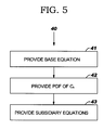
- FIG. 5 is a flow chart for providing a model for a characteristic C distributed in a domain wherein the characteristic C is not expressed in terms of subcharacteristics of C, in accordance with embodiments of the present invention.
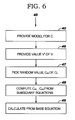
- FIG. 6 is a flow chart for randomly sampling C based on the model provided in FIG. 5 , in accordance with embodiments of the present invention.
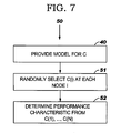
- FIG. 7 is a flow chart for determining a performance parameter of a design based on the model of C in FIG. 5 and on the method for sampling C in FIG. 6 , in accordance with embodiments of the present invention.
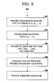
- FIG. 8 is a flow chart for providing a model for a characteristic C distributed in a domain wherein the characteristic C is expressed in terms of subcharacteristics of C, in accordance with embodiments of the present invention.
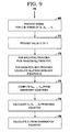
- FIG. 9 is a flow chart for randomly sampling C based on the model provided in FIG. 8 , in accordance with embodiments of the present invention.
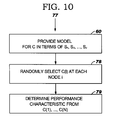
- FIG. 10 is a flow chart for determining a performance parameter of a design based on the model of C in FIG. 8 and on the method for sampling C in FIG. 9 , in accordance with embodiments of the present invention.
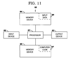
- FIG. 11 illustrates a computer system used for implementing one or more algorithms that model a characteristic of a design, in accordance with embodiments of the present invention.
- the present invention relates to the design of a physical system comprising devices therein such that characteristics of the devices are subject to uncertainty.
- a physical system may comprise integrated circuits on a semiconductor wafer, wherein characteristics (e.g., capacitance) of devices (e.g., virtual capacitors) on the wafer may be subject to uncertainty due to process variations that occur during manufacturing of the integrated circuits on the semiconductor wafer.
- the designer e.g., the integrated circuit designer
- such performance characteristics may include, inter alia, signal transmission speed, signal switching speed, operating temperature, power output, power conversion efficiency, the logical correctness of a logic circuit, etc.
- the computerized simulation takes into account the uncertainty, such as uncertainty due to process variations, in the device characteristics by the methodology of the present invention.
- the uncertainties are modeled by one or more probability density functions, such as a normal probability distribution characterized by a mean and a standard deviation.
- other examples of device characteristics in electrical systems include, inter alia, the resistance of a metal line, the inductance of an inductor, and the threshold voltage of a transistor.
- the subsequent description of the present invention is divided into four segments.
- the first segment illustrates the present invention by discussing the modeling of the characteristic C of the capacitance of a varactor, which is a capacitor whose capacitance varies with the applied voltage.
- the second segment formulates the present invention generally by discussing the modeling of a characteristic C that is distributed within a domain, wherein C is not expressed in terms of any subcharacteristics of C, as embodied in Equation (2) discussed infra.
- the third segment formulates the present invention generally by discussing the modeling of a characteristic C that is distributed within a domain, wherein C is expressed in terms of a plurality of subcharacteristics of C, as embodied in Equation (3) discussed infra.
- the fourth segment describes a computer system that may be utilized to implement algorithms of the present invention.
- a particular example of a device in an integrated circuit is a varactor built in a semiconductor via by implanting and diffusing dopant impurities to create a p-n junction.
- the varactor described by Equation (1) is a “virtual capacitor” as contrasted with a physical capacitor that has two conducting plates separated by a dielectric medium such as air.
- a virtual capacitor has virtual capacitor plates with an effective area and an effective perimeter.
- the effective plate area represents the region of the p-n junction having uniform depth
- the effective plate perimeter represents the regions of the diffused p-n junction which is not of uniform depth, typically on the edges of the diffused region.
- a real or virtual capacitor may be characterized by an area capacitance and a perimeter capacitance.
- Area capacitance is defined as capacitance per unit area of a physical capacitor plate if the capacitor is a physical capacitor, or the capacitance per unit effective area of a virtual capacitor plate if the capacitor is a virtual capacitor.
- Perimeter capacitance is defined as capacitance per unit perimeter of a physical capacitor plate if the capacitor is a physical capacitor, or the capacitance per unit effective perimeter of a virtual capacitor plate if the capacitor is a virtual capacitor.
- the scope of the present invention includes both physical devices and virtual devices.
- Equation (1) the parameters C 0 , V B , and m are subject to uncertainty, such as due to process variations, and are modeled statistically in accordance with the present invention. Note that Equation (1) has a physical basis for describing the capacitance C of a varactor and may accurately describe a varactor in many situations. In some situation, however, an equation with more adjustable parameters than the three parameters (C 0 , V 0 , and m) in Equation (1) may be useful for fitting measured capacitances.
- Equation (1) V is the applied voltage.
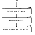
- the fifth order polynomial in V of Equation (2) has no physical basis for describing the hyperabrupt varactor and is utilized because the fifth order polynomial in Equation (2) can be accurately fitted to measured total capacitances of hyperabrupt varactors as a function of applied voltage, as illustrated in FIG. 1 in accordance with embodiments of the present invention.
- the total capacitances of 5 devices on each of 12 dies were measured from which the data shown in FIG. 1 are drawn. This measured data was used to extract area and perimeter capacitances for each device.
- Each die of the 12 dies had five devices and one device was selected from each die for the data shown in FIG. 1 . All 5 devices were located close to one another (i.e., within about 3000 microns) on the same die.
- the anode to cathode voltage of the varactor is swept from slightly forward bias to relatively large reverse bias but less than the onset of avalanche multiplication.
- FIG. 1 shows that the nominal curve 10 fitted in accordance with Equation (2) accurately models the measured capacitances.
- the nominal curve 10 of FIG. 1 which is fitted in accordance with Equation (2), accurately models the measured capacitances, the nominal curve 10 does not account for uncertainties in the capacitance C due to process variations.
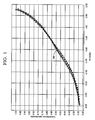
- FIG. 2 illustrates capacitance versus voltage curves obtained by selecting C 0 , C 1 , C 2 , C 3 , C 4 , and C 5 as being randomly distributed about a nominal fit to Equation (2) (e.g., the nominal fit 10 of FIG. 1 described supra), in accordance with embodiments of the present invention.
- a nominal fit to Equation (2) e.g., the nominal fit 10 of FIG. 1 described supra
- Equation 2 The parameters C 0 , C 1 , C 2 , C 3 , C 4 , and C 5 were randomly sampled independently and the resultant values of C 0 , C 1 , C 2 , C C 4 , and C 5 were substituted into Equation 2 to generate the curves of FIG. 2 .
- the curve 20 represents a nominal fit to Equation (2), whereas curves 21 - 29 were generated using sampling constraints.
- each coefficient of the set of coefficients (i.e., C 0 , C 1 , C 2 , C 3 , C 4 , and C 5 ) was independently randomly selected from a normal distribution characterized by a mean equal to the nominal value of the coefficient and a standard deviation a such that 3 ⁇ is 10% of the nominal value of the coefficient (e.g., if the nominal value is 3 then ⁇ is 0.1).
- each curve of curves 21 - 29 has a unique set of coefficients randomly selected as described supra, such that the voltage was varied for the unique set of coefficients.
- the inventors of the present invention have determined that the non-physical nature of the curves 21 - 29 in FIG. 2 is caused by randomly varying the parameters C 0 , C 1 , C 2 , C 3 , C 4 , and C 5 independently, which is equivalent to having six degrees of statistical freedom.
- the six independent degrees of statistical freedom is incorrect because to have a physically realistic result there should be only one degree of statistical freedom.
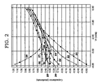
- FIGS. 3A-3E which shows five correlating relationships among the six parameters C 0 , C 1 , C 2 , C 3 , C 4 , and C 5 , in accordance with embodiments of the present invention.
- Equation (2) if C 0 is permitted to vary randomly in conjunction with Equation (2), then the other parameters C 1 , C 2 , C 3 , C 4 , and C 5 are determined by being correlated with C 0 , as shown for the area capacitance coefficients plotted in FIGS. 3A-3E .
- the total capacitances of 5 devices on each of 42 dies were measured from which the area capacitance coefficients shown in FIGS. 3A-3E are drawn. This measured data was used to extract the area and perimeter capacitances. All 5 devices were located close to one another (i.e., within about 3000 microns) on the same die. All 42 dies were used to generate the area capacitance coefficient data shown in FIG. 1 . Forty-two sets of polynomial coefficients were determined from these 42 die to model the area capacitance and another 42 sets of polynomial coefficients were determined from these 42 die to model the perimeter capacitance. Regression analyses of the polynomial coefficients used to model the area capacitance are shown in FIGS. 3A-3E .
- FIGS. 3A-3E each show a data curve and a curve representing a quadratic fit to the data.
- FIG. 3A depicts C 1 versus C 0
- FIG. 3B depicts C 2 versus C 1
- FIG. 3C depicts C 3 versus C 2
- FIG. 3D depicts C 4 versus C 3
- FIG. 3E depicts C 5 versus C 4 .
- the correlations shown in FIGS. 3A-3E are equivalent to C 1 , C 2 , C 3 , C 4 , and C 5 being each correlated with C 0 .
- the fitted curves are only slightly quadratic and appear to be nearly linear in shape.
- 3A-3E are slightly quadratic and nearly linear, the shape of the curves of C 1 , C 2 , C 3 , C 4 , and C 5 versus C 0 may generally be linear, quadratic, or any other shape as determined empirically or by an analytical method.
- the correlations in FIGS. 3A-3E are of quadratic form, any functional dependence of C 1 , C 2 , C 3 , C 4 , and C 5 on C 0 is within the scope of the present invention.
- C 1 , C 2 , C 3 , C 4 , and C 5 are each correlated with C 0 and there is thus only one degree of statistical freedom among C 0 , C 1 , C 2 , C 3 , C 4 , and C 5 .
- the method of the present invention picks C 0 randomly from a probability density function (PDF) of C 0 and uses correlations such as shown in FIGS. 3A-3E to determine C 1 , C 2 , C 3 , C 4 , and C 5 from the picked value of C 0 .
- PDF probability density function
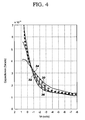
- FIG. 4 which shows total capacitance versus applied voltage curves, in accordance with embodiments of the present invention.
- the total capacitances of 5 devices on each of 42 dies were measured from which the data shown in FIG. 4 are drawn. This measured data was used to extract area and perimeter capacitances.
- Each die of the 42 dies had five devices and one device was selected from each die for the data shown in FIG. 4 . All 5 devices were located close to one another (i.e., within about 3000 microns) on the same die.
- the anode to cathode voltage of the varactor is swept from slightly forward bias to relatively large reverse bias but less than the onset of avalanche multiplication.
- dashed lines 30 represent test data exhibiting characterized by process variations
- line 32 represents a nominal fit of Equation (2) to the test data
- bounding curves 34 and 36 representing the limiting envelope of simulated process variations in conjunction with Equation (2) by picking C 0 randomly from its PDF and calculating C 1 , C 2 , C 3 , C 4 , and C 5 from the picked value of C 0 through the correlations analogous to those shown in FIGS. 3A-3E .
- FIG. 4 shows that curves 34 and 36 envelope the test data in a manner that confirms the accuracy of the method of the present invention in using Equation (2) to model the test data.
- the PDF for C 0 may be determined as follows. Capacitance C 0 at zero applied voltage may be measured at a multiplicity of points on a wafer and/or on different wafers, resulting in a corresponding multiplicity of capacitances C 0 which reflect a variety of process variations.
- the measured multiplicity of capacitances may be fitted to a probability density function such, inter alia, as a normal probability distribution by any method known to a person of ordinary skill in the art (e.g., by calculating the mean of the normal distribution as the arithmetic mean of the measured capacitances, and by calculating the standard deviation of the normal distribution as the standard deviation of the measured capacitances).
- a method for developing a model for incorporating process variability comprises determining a PDF for C 0 ; and correlating C 1 , C 2 , C 3 , C 4 , and C 5 with C 0 as discussed supra in conjunction with FIGS. 3A-3E .
- a method for assessing a design that includes capacitance subject to process variations comprises: evaluating a performance characteristic of the design (e.g., signal transmission speed, signal switching speed, operating temperature, power output, power conversion efficiency, the logical correctness of a logic circuit, etc.) by simulating the design.
- a performance characteristic of the design e.g., signal transmission speed, signal switching speed, operating temperature, power output, power conversion efficiency, the logical correctness of a logic circuit, etc.
- the determined values of C at the nodes are utilized to determine the performance characteristic.
- the performance characteristic of switching speed may be a function of the values of capacitances C( 1 ), C( 2 ), . . . so determined.
- any of the other parameters C 1 , C 2 , C 3 , C 4 , and C 5 could have alternatively been randomly picked instead of C 0 .
- C 1 could have been picked randomly from its PDF and the other parameters C 0 , C 2 , C 3 , C 4 , and C 5 would be calculated from their correlations with C 1 .
- Equation (1) is suitable for calculating capacitance in some applications and may be utilized as follows.
- PDF probability density function
- the capacitance C in Equation (1) may be randomly sampled by picking a value of C 0 from its PDF; calculating V B and m from their correlation with C 0 ; and substitute the picked value of C 0 and the calculated values of V B and m into Equation (1) to determine C.
- the capacitance of a physical or virtual capacitor may be expressed in terms of area capacitance C A and perimeter capacitance C P via Equation (3).
- C A*C A +P*C P (Equation 3)
- An algorithm of the present invention determines C A and C P by random sampling; and substituting C A and C P into Equation (3) to obtain C.
- C A and C P may be calculated independently or correlatively, depending on whether C 0A and C 0P are sufficiently correlated.
- a correlation between C 0A and C 0P may be deduced from scatter data of C 0A as a function of C 0P , wherein the points of the scatter data may represent pairs of (C 0A , C 0P ) at a variety of locations on a wafer and/or several wafers.
- each pair of (C A , C P ) may be deduced from Equation (3), by measuring C for at least two sufficiently close locations on the wafer (e.g., on a kerf surrounding a semiconductor chip) at which C A and C P are not expected to vary due to process variation. Therefore at zero applied voltage V, each pair of (C 0A , C 0P ) may be deduced from Equation (3) by measuring C (at zero volts) for least two sufficiently close locations on the wafer at which C 0A and C 0P are not expected to vary due to process variation.
- (C A , C P ) and (C 0A , C 0P ) may generally be inferred from measurement of total capacitance C for at least two sufficiently close locations on the wafer, at a given non-zero applied voltage V and a given zero applied voltage V, respectively.
- a correlation coefficient r (e.g., a Pearson correlation coefficient) may be calculated from the scatter data of C 0A versus C 0P .
- C 0A and C 0P may be considered as being sufficiently correlated if the correlation parameter R is no less than a specified value R MIN (e.g., R MIN may be in a range of, inter alia, 0.70-0.90).
- C 0A may be regressed upon C 0P to determine an equation that correlates C 0A with C 0P .
- C 0P may be picked randomly from its PDF and C 0A may then be calculated from the equation that correlates C 0A with C 0P .
- C 0A may be picked randomly from its PDF and C 0P may then be calculated from the equation that correlates C 0P with C 0A which is the inverse of the equation that correlates C 0A with C 0P .
- C 0A and C 0P may be independently picked randomly from their respective PDFs.
- the coefficients C 1A , C 2A , C 3A , C 4A , C 5A of Equation (4) are each correlated with C 0A in a manner analogous to the correlation of C 1 , C 2 , C 3 , C 4 , and C 5 with C as described supra in conjunction with FIGS. 3A-3E .
- the coefficients C 1P , C 2P , C 3P , C 4P , C 5P of Equation (5) are each correlated with C 0P in a manner analogous to the correlation of C 1 C 2 , C 3 , C 4 , and C 5 with C 0 as described supra in conjunction with FIGS. 3A-3E .
- C 0A and C 0P are determined as described supra, the remaining sets of coefficients (C 1A , C 2A , C 3A , C 4A , C 5A ) and (C 1P , C 2P , C 3P , C 4P , C 5P ) are determined from their correlation with C 0A and C 0P , respectively.
- C A and C P may be calculated from Equations (4) and (5), respectively, which enables C to be subsequently determined by substituting C A and C P into Equation (3).
- the determined values of C at the locations in the design are then utilized to determine the performance characteristic.
- the performance characteristic of switching speed may be a function of the values of capacitance C so determined.
- the preceding discussion of FIGS. 1-4 and Equations 1-5 for the example of the capacitance of a varactor will next be extended in the second and third segments of the description herein to formulate the scope of the present invention in its generality.
- the second segment of the description herein formulates the present invention generally by discussing the modeling of a characteristic C that is distributed within a domain, wherein C is not expressed in terms of any subcharacteristics of C.
- the third segment of the description herein formulates the present invention generally by discussing the modeling of a characteristic C that is distributed within a domain, wherein C is expressed in terms of a plurality of subcharacteristics of C.
- the present invention discloses a method for statistically modeling a characteristic C that is distributed within a domain, wherein C is a function of a variable V, and wherein C is not expressed in terms of subcharacteristics, as embodied in the example of Equation (2) discussed supra.
- the domain may be a physical domain (e.g., a physical surface or volume) such as, inter alia, a semiconductor wafer comprising integrated circuits, a geographic neighborhood comprising houses, a galaxy comprising stars, etc.
- the characteristic C may be capacitance and the variable V may be applied voltage, as discussed supra in conjunction with Equation (2).
- the domain may also be a non-physical domain such as, inter alia, the domain of stocks on the New York Stock Exchange, wherein the characteristic C may be, inter alia, the price-to-earnings (PE) ratio of each stock and the variable V may be, inter alia, an interest rate benchmark (e.g., the Federal Funds interest rate).
- PE price-to-earnings
- FIG. 5 is a flow chart for providing a model for representing the characteristic C.
- FIG. 6 is a flow chart for randomly sampling C based on the model for C described by FIG. 5 .
- FIG. 7 is a flow chart for determining a performance characteristic of a design, based on the model of C in FIG. 5 and the method for randomly sampling C in FIG. 6 .
- FIG. 5 is a flow chart 40 depicting steps 41 - 43 which describe providing a model for C.
- Step 41 provides a base equation for modeling C.
- the base equation expresses the characteristic C as a function f of the variable V through use of N+1 parameters C 0 , C 1 , . . . , C N .
- Step 42 provides a probability density function (PDF) for describing the probability of occurrence of C 0 in accordance with the uncertainty in C 0 .
- PDF may be a normal probability distribution or any other form of probability distribution.
- This methodology for providing the PDF of C 0 from test data may be formulated by postulating that the domain comprises nodes such that test data is obtained at the nodes.
- the nodes may each correspond to an integrated circuit on a wafer.
- the PDF of C 0 is derived from the aforementioned test data as described supra; i.e., by any method known to a person of ordinary skill in the art of fitting a functional form of a PDF to test data.
- the discussion supra provides an explanation of how the PDF of C 0 may be determined from an analysis of test data.
- the scope of the present invention includes determining the PDF of C 0 not only from test data, but alternatively by any other method such as from an analytical calculation or from computer simulation based on an assumed analytical model.
- Step 43 provides subsidiary equations expressing C 1 , . . . , C N in terms of C 0 .
- C x is a linear of quadratic function g x of C x-1
- the parameter C x may generally be any function g x of C x-1 which accurately represents the functional relationship between C x and C x-1 .
- test data of C(k) versus V may be obtained at each node k of K nodes, wherein K is at least 2, wherein a “node” is a different location in the region of testable devices (e.g., test sites on a wafer), wherein C(k) is defined as C at node k, and wherein k has values of 1, 2, . . . , K.
- C N (k) respectively denote C 0 , C 1 , . . . , C N at node k.
- a curve of a given analytical form e.g., linear, quadratic, exponential, etc.
- FIG. 6 is a flow chart 45 depicting steps 40 and 46 - 49 for randomly sampling C.
- Step 40 is the flow chart 40 of FIG. 5 which provides the model for C, described supra. Given the model for C provided by step 40 , steps 46 - 49 are executed when a value of C is to be randomly sampled.
- Step 46 provides a value V′′ of V as input to the process of randomly sampling C.
- Step 47 picks a random value C 0R of C 0 from the PDF of C 0 , wherein the PDF was provided in step 42 of FIG. 5 as described supra.
- any method for picking C 0R from the PDF may be utilized (e.g., picking C 0R by utilizing the cumulative probability distribution associated with the PDF as is known in the art).
- Step 48 computes values C 1R , . . . , C NR of C 1 , . . . , C N , respectively, by substituting C 0R into the subsidiary equations that were provided in step 43 of FIG. 5 , described supra.
- Step 49 calculates C by substituting C 0R , C 1R , . . . , C NR and V′′ into the base equation provided in step 41 of FIG. 5 .
- FIG. 7 is a flow chart 50 depicting steps 40 and 51 - 52 for determining a performance characteristic of a design, based on the model of C in FIG. 5 and the method for randomly sampling C in FIG. 6 .
- the design comprises I nodes in the domain in which C is distributed, wherein I is at least 2.
- Each node i of the I nodes has a value C(i) of the characteristic C, wherein i has values of 1, 2, . . . , I.
- Step 40 is the flow chart 40 of FIG. 5 which provides the model for C, described supra.
- step 51 randomly selects a value of C(i) of C at each node i of the I nodes.
- step 51 is implemented by executing steps 46 - 49 of FIG. 6 , wherein V′′ in step 46 is V(i).
- V(i) is defined as the value of V at node i, which is input to the calculation of C(i) as discussed supra in conjunction with step 46 of FIG. 6 .
- step 52 determines the performance characteristic, by utilizing the randomly selected values of C( 1 ), C( 2 ), . . . , C(I).
- the present invention discloses a method for statistically modeling a characteristic C that is distributed within a domain, wherein C is a function of a variable V, and wherein C is expressed in terms of J subcharacteristics S 1 , S 2 , . . . , S J , as embodied in the example of Equation (3) discussed supra.
- the domain may be a physical domain (e.g., a physical surface or volume) such as, inter alia, a semiconductor wafer comprising integrated circuits, a geographic neighborhood comprising houses, a galaxy comprising stars, etc.
- the characteristic C may be capacitance
- the variable V may be applied voltage, as discussed supra in conjunction with Equation (3).
- PE price-to-earnings
- FIG. 8 is a flow chart for providing a model for representing the characteristic C in terms of its J subcharacteristics S 1 , S 2 , . . . , S J .
- FIG. 9 is a flow chart for randomly sampling C based on the model for C and its subcharacteristics described by FIG. 8 .
- FIG. 10 is a flow chart for determining a performance characteristic of a design, based on the model of C and its subcharacteristics in FIG. 8 and the method for randomly sampling C in FIG. 9 .
- FIG. 8 is a flow chart 60 depicting steps 61 - 65 which describe providing a model for C.
- Step 61 provides a combination equation for modeling C as a function F its J subcharacteristics S 1 , S 2 , . . . , S J .
- Step 62 provides base equations which express S j as a function f j of a variable V through use of N+1 parameters S j0 , S j1 , . . . , S jN .
- f j may have various functional characteristics.
- a first example of a functional characteristic for f j is that f j may have a same functional form of V for each subcharacteristic S j of the J subcharacteristics (e.g., a fifth order polynomial in V for each S j ).
- a second example of a functional characteristic for f j is that f j may be constant with respect to any variation in V for each subcharacteristic S j of the J subcharacteristics (i.e., f j does not depend on V).
- a third example of a functional characteristic for f j is that f j may vary with respect to a variation in V for each subcharacteristic S j of the J subcharacteristics (i.e., each f j varies with V).
- Step 63 provides at least one probability density function (PDF) selected from PDF 1 , PDF 2 , . . . , PDF J .
- PDF 1 , PDF 2 , . . . , PDF J may each be a normal probability distribution or any other form of probability distribution. At least one PDF n is provided and PDF 1 is always provided. Thus for n>0, none, some, or all of the PDF n may be provided. If provided, PDF n may be determined by any method described supra for determining the PDF of C 0 , including test methods, analytical calculation, or computer simulation based on an assumed analytical model.
- PDF 1 is always provided.
- PDF n (for n>0) is not provided if S n0 is sufficiently correlated with S 10 .
- S n0 is sufficiently correlated with S 10 if a correlation parameter R n between S n0 and S 10 is no less than a specified minimum correlation parameter R MIN .
- the correlation parameter R n is the square of a correlation coefficient r n between S n0 and S 10 .
- the correlation coefficient r n may be determined from scatter data of S n0 versus S 10 as described supra.
- step 64 For each PDF n not provided, step 64 provides an auxiliary equation E n expressing S n0 in terms of S 10 which is analogous to the aforementioned relating of C 0A to C 0P to determine an equation correlating C 0A with C 0P , as discussed supra.
- the auxiliary equation E n may be derived from the scatter data of S n0 versus S 10 .
- Step 65 provides subsidiary equations expressing S j1 , . . . , S jN in terms of S j0 for each subcharacteristic S j of the J subcharacteristics, which for a fixed j are analogous to the subsidiary equations expressing C 1 , . . . , C N in terms of C 0 as described supra in conjunction with FIGS. 3A-3E .
- the subsidiary equations for calculating S j1 , . . . , S jN in terms of S j0 (for fixed j) may be derived by any of the methods described supra for deriving the subsidiary equations for calculating C 1 , . . . , C N in terms of C 0 .
- FIG. 9 is a flow chart 70 depicting steps 60 and 71 - 75 for randomly sampling C.
- Step 60 is the flow chart 60 of FIG. 8 which provides the model for C in terms of its J subcharacteristics S 1 , S 2 , . . . , S J , described supra.
- steps 71 - 75 are executed when a value of C is to be randomly sampled.
- Step 71 provides a value V′′ of V as input to the process of randomly sampling C.
- step 72 For each PDF n provided in step 63 of FIG. 8 (including PDF 1 ), step 72 picks a random value of S n0R from PDF n . For each PDF n not so provided, step 72 calculates S n0R by substituting S 10R into the auxiliary equation E n provided in step 64 of FIG. 8 .
- Step 73 computes values S j1R , . . . , S jNR of S j1 , . . . , S jN , respectively, by substituting S j0R into the subsidiary equations provided by step 65 of FIG. 8 for each subcharacteristic S j of the J subcharacteristics.
- Step 74 calculates S j by substituting S j0R , S j1R , . . . , S jNR and V′′ into the base equations provided by step 62 of FIG. 8 for each subcharacteristic S of the J subcharacteristics
- Step 75 calculates C by substituting S 1 , S 2 , . . . , S J into the combination equation provided by step 61 of FIG. 8 .
- FIG. 10 is a flow chart 77 depicting steps 60 and 78 - 79 for determining a performance characteristic of a design, based on the model of C in FIG. 8 and the method for randomly sampling C in FIG. 9 .
- the design comprises I nodes in the domain in which C is distributed, wherein I is at least 2.
- Each node i of the I nodes has a value C(i) of the characteristic C, wherein i has values of 1, 2, . . . , I.
- Step 60 is the flow chart 60 of FIG. 8 which provides the model for C in terms of its J subcharacteristics S 1 , S 2 , . . . , S J , described supra.
- step 78 randomly selects a value of C(i) of C at each node i of the I nodes.
- step 78 is implemented by executing steps 71 - 75 of FIG. 9 , wherein V′′ in step 71 is V(i).
- V(i) is defined as the value of V at node i, which is input to the calculation of C(i) as discussed supra in conjunction with step 71 of FIG. 9 .
- step 79 determines the performance characteristic, by utilizing the randomly selected values of C( 1 ), C( 2 ), . . . , C(I).
- Equation 10 While the description of embodiments of the present invention has focused on modeling a characteristic C or subcharacteristic S j that depends on a single independent variable V, the scope of the present invention also includes modeling C and S j each as a function of a plurality of independent variables V 1 , V 2 , . . . , wherein the base Equations (6) and (8) for C and S j would be respectively generalized to Equations (9) and (10):
- C f ( C 0 , C 1 , . . . , C N , V 1 , V 2 , . . . ) (Equation 9)
- S j f j ( Sj 0 , S j1 , . . . , S jN , V 2 , . . . ) (Equation 10)
- the dependence of C and/or S j on V 1 , V 2 , . . . . may be individually tailored for each of V 1 , V 2 , . . . and may be cast in any applicable functional form for each independent variable such as, inter alia, the polynomial functional form of Equation (2) and/or Equations (4)-(5).
- the parameters C 0 , C 1 , . . . C N would be coupled to the variables V 1 , V 2 , . . . in a manner that reflects the functional forms chosen. For example for the case of fitting C to a polynomial in each independent variable of two independent variables V 1 and V 2 , some of the parameters of C 0 , C 1 , . . .
- the parameter C 0 for the multiple independent variable V 1 , V 2 , . . . embodiment would be picked from its PDF and parameters C 1 , . . . , C N would be determined based on their relationship to C 0 as expressed in subsidiary equations in accordance with the description supra thereof.
- FIG. 11 illustrates a computer system 90 used for implementing algorithms that model and sample a characteristic C (and assess a design comprising C), in accordance with embodiments of the present invention.
- the computer system 90 comprises a processor 91 , an input device 92 coupled to the processor 91 , an output device 93 coupled to the processor 91 , and memory devices 94 and 95 each coupled to the processor 91 .
- the input device 92 may be, inter alia, a keyboard, a mouse, etc.
- the output device 93 may be, inter alia, a printer, a plotter, a computer screen, a magnetic tape, a removable hard disk, a floppy disk, etc.
- the memory devices 94 and 95 may be, inter alia, a hard disk, a floppy disk, a magnetic tape, an optical storage such as a compact disc (CD) or a digital video disc (DVD), a dynamic random access memory (DRAM), a readonly memory (ROM), etc.
- the memory device 95 includes a computer code 97 .
- the computer code 97 includes one or more algorithms that model and sample the characteristic C (and assess a design comprising C), in accordance with embodiments of the present invention.
- the processor 91 executes the computer code 97 .
- the memory device 94 includes input data 96 .
- the input data 96 includes input required by the computer code 97 .
- the output device 93 displays output from the computer code 97 .
- Either or both memory devices 94 and 95 may be used as a computer usable medium (or a computer readable medium or a program storage device) having a computer readable program code embodied therein and/or having other data stored therein, wherein the computer readable program code comprises the computer code 97 .
- a computer program product (or, alternatively, an article of manufacture) of the computer system 90 may comprise said computer usable medium (or said program storage device).
- FIG. 11 shows the computer system 90 as a particular configuration of hardware and software
- any configuration of hardware and software may be utilized for the purposes stated supra in conjunction with the particular computer system 90 of FIG. 11 .
- the memory devices 94 and 95 may be portions of a single memory device rather than separate memory devices.
Abstract
Description
- 1. Technical Field
- The present invention relates to a method and model for incorporating uncertainty information when modeling a characteristic of a design.
- 2. Related Art
- An integrated circuit is subject to process variations that occur during manufacture of integrated circuits. Circuit designers currently assess the effect these process variations on performance characteristics of integrated circuits by methods which do not yield sufficiently accurate assessments. Thus, there is a need for a method that assesses the effect of process variations on performance characteristics of integrated circuits more accurately than is accomplished in the related art.
- The present invention provides a method for modeling a characteristic C that is distributed within a domain, said method comprising:
-
- providing a base equation expressing the characteristic C as a function f of a variable V through use of N+1 parameters C0, C1, . . . , CN, said base equation being of the form C=f(C0, C1, . . . , CN, V), said N being at least 1, said parameters C0, C1, . . . , CN being subject to uncertainty;
- providing a probability density function (PDF) for describing the probability of occurrence of C0 in accordance with said uncertainty; and
- providing subsidiary equations expressing C1, . . . , CN in terms of C0.
- The present invention provides a method for modeling a characteristic C that is distributed within a domain, said characteristic C having J subcharacteristics S1, S2, . . . , SJ, said method comprising:
-
- providing a combination equation that expresses C as a function F of the J subcharacteristics, said J being at least 2;
- providing base equations expressing Sj as a function fj of a variable V through use of N+1 parameters Sj0, Sj1, . . . , SjN, said base equations being of the form Sj=fj(Sj0, Sj1, . . . , SjN, V), said N being at least 1, said parameters Sj0, Sj1, . . . , SjN being subject to uncertainty, said j having values of 1, 2, . . . , J;
- providing at least one probability density function (PDF) from PDF1, PDF2, . . . PDFJ, said PDFn describing the probability of occurrence of Sn0 in accordance with said uncertainty for n=1, 2, . . . , J, said at least one PDF including PDF1;
- for each PDFn not provided: providing an auxiliary equation En expressing Sn0 in terms of S10; and
- providing subsidiary equations expressing Sj1, . . . , SjN in terms of Sj0 for each subcharacteristic Sj of the J subcharacteristics.
- The present invention provides a computer program product, comprising a computer usable medium having a computer readable program code embodied therein, said computer readable program code adapted to be executed on a processor for implementing a method for modeling a characteristic C that is distributed within a domain, said method comprising:
-
- providing a base equation expressing the characteristic C as a function f of a variable V through use of N+1 parameters C0, C1, . . . , CN, said base equation being of the form C=f(C0, C1, . . . , CN, V), said N being at least 1, said parameters C0, C1, . . . , CN being subject to uncertainty;
- providing a probability density function (PDF) for describing the probability of occurrence of C0 in accordance with said uncertainty; and
- providing subsidiary equations expressing C1, . . . , CN in terms of C0.
- The present invention provides a computer program product, comprising a computer usable medium having a computer readable program code embodied therein, said computer readable program code adapted to be executed on a processor for implementing a method for modeling a characteristic C that is distributed within a domain, said characteristic C having J subcharacteristics S1, S2, . . . , SJ, said method comprising:
-
- providing a combination equation that expresses C as a function F of the J subcharacteristics, said J being at least 2;
- providing base equations expressing Sj as a function fj of a variable V through use of N+1 parameters Sj0, Sj1, . . . , SjN, said base equations being of the form Sj=fj(Sj0, Sj1, . . . , SjN, V), said N being at least 1, said parameters Sj0, Sj1, . . . , SjN being subject to uncertainty, said j having values of 1, 2, . . . , J;
- providing at least one probability density function (PDF) from PDF1, PDF2, PDFJ, said PDFn describing the probability of occurrence of Sn0 in accordance with said uncertainty for n=1, 2, . . . , J, said at least one PDF including PDF1;
- for each PDFn not provided: providing an auxiliary equation En expressing Sn0 in terms of S10; and
- providing subsidiary equations expressing Sj1, . . . , SjN in terms of Sj0 for each subcharacteristic Sj of the J subcharacteristics.
- The present invention provides a model, comprising:
-
- a base equation expressing a characteristic C as a function f of a variable V through use of N+1 parameters C0, C1, . . . , CN, said base equation being of the form C=f(C0, C1, . . . , CN, V), said N being at least 1, said parameters C0, C1, . . . , CN being subject to uncertainty, said characteristic C being distributed within a domain;
- a probability density function (PDF) for describing the probability of occurrence of C0 in accordance with said uncertainty; and
- subsidiary equations expressing C1, . . . , CN in terms of C0.
- The present invention provides a model, comprising:
-
- a combination equation that expresses C as a function F of the J subcharacteristics, said J being at least 2, said characteristic C being distributed within a domain, said characteristic C having J subcharacteristics S1, S2, . . . , SJ;
- base equations expressing Sj as a function fj of a variable V through use of N+1 parameters Sj0, Sj1, . . . , SjN, said base equations being of the form Sj=fj(Sj0, Sj1, . . . , SjN, V), said N being at least 1, said parameters Sj0, Sj1, . . . , SjN being subject to uncertainty, said j having values of 1, 2, . . . , J;
- at least one probability density function (PDF) from PDF1, PDF2, . . . , PDFJ, said PDFn describing the probability of occurrence of Sn0 in accordance with said uncertainty for n=1, 2, . . . , J, said at least one PDF including PDF1;
- for each PDFn that does not exist: an auxiliary equation En expressing Sn0 in terms of S10; and
- subsidiary equations expressing Sj1, . . . , SjN in terms of Sj0 for each subcharacteristic Sj of the J subcharacteristics.
- The present invention provides a method that assesses the effect of process variations on performance characteristics of integrated circuits more accurately than is accomplished in the related art.
-
FIG. 1 depicts a nominal curve of capacitance versus applied voltage of a varactor fitted to a fifth order polynomial in the applied voltage, in accordance with embodiments of the present invention. -
FIG. 2 depicts the effect of process variations on the nominal curve ofFIG. 1 based on six independent degrees of statistical freedom, in accordance with embodiments of the present invention. -
FIGS. 3A-3E depict curves relating parameters used for modeling the capacitance of a varactor with each other, in accordance with embodiments of the present invention. -
FIG. 4 depicts the effect of process variations on the nominal curve ofFIG. 1 based on one independent degree of statistical freedom, in accordance with embodiments of the present invention. -
FIG. 5 is a flow chart for providing a model for a characteristic C distributed in a domain wherein the characteristic C is not expressed in terms of subcharacteristics of C, in accordance with embodiments of the present invention. -
FIG. 6 is a flow chart for randomly sampling C based on the model provided inFIG. 5 , in accordance with embodiments of the present invention. -
FIG. 7 is a flow chart for determining a performance parameter of a design based on the model of C inFIG. 5 and on the method for sampling C inFIG. 6 , in accordance with embodiments of the present invention. -
FIG. 8 is a flow chart for providing a model for a characteristic C distributed in a domain wherein the characteristic C is expressed in terms of subcharacteristics of C, in accordance with embodiments of the present invention. -
FIG. 9 is a flow chart for randomly sampling C based on the model provided inFIG. 8 , in accordance with embodiments of the present invention. -
FIG. 10 is a flow chart for determining a performance parameter of a design based on the model of C inFIG. 8 and on the method for sampling C inFIG. 9 , in accordance with embodiments of the present invention. -
FIG. 11 illustrates a computer system used for implementing one or more algorithms that model a characteristic of a design, in accordance with embodiments of the present invention. - The present invention relates to the design of a physical system comprising devices therein such that characteristics of the devices are subject to uncertainty. For example, a physical system may comprise integrated circuits on a semiconductor wafer, wherein characteristics (e.g., capacitance) of devices (e.g., virtual capacitors) on the wafer may be subject to uncertainty due to process variations that occur during manufacturing of the integrated circuits on the semiconductor wafer. To confirm that such a design is acceptable, the designer (e.g., the integrated circuit designer) may assess the design by computerized simulation of the system for determining whether performance characteristics of the system are within acceptable limits. For integrated circuit design, such performance characteristics may include, inter alia, signal transmission speed, signal switching speed, operating temperature, power output, power conversion efficiency, the logical correctness of a logic circuit, etc. The computerized simulation takes into account the uncertainty, such as uncertainty due to process variations, in the device characteristics by the methodology of the present invention. The uncertainties are modeled by one or more probability density functions, such as a normal probability distribution characterized by a mean and a standard deviation. In addition to capacitance, other examples of device characteristics in electrical systems include, inter alia, the resistance of a metal line, the inductance of an inductor, and the threshold voltage of a transistor.
- The subsequent description of the present invention is divided into four segments. The first segment illustrates the present invention by discussing the modeling of the characteristic C of the capacitance of a varactor, which is a capacitor whose capacitance varies with the applied voltage. The second segment formulates the present invention generally by discussing the modeling of a characteristic C that is distributed within a domain, wherein C is not expressed in terms of any subcharacteristics of C, as embodied in Equation (2) discussed infra. The third segment formulates the present invention generally by discussing the modeling of a characteristic C that is distributed within a domain, wherein C is expressed in terms of a plurality of subcharacteristics of C, as embodied in Equation (3) discussed infra. The fourth segment describes a computer system that may be utilized to implement algorithms of the present invention.
- Modeling the Capacitance of a Varactor
- A particular example of a device in an integrated circuit is a varactor built in a semiconductor via by implanting and diffusing dopant impurities to create a p-n junction. Such a varactor may be described by Equation (1):
C=C 0/(1−V/V B)m (Equation 1) -
- where C is the capacitance of the varactor, VB is the ‘built-in’ voltage (VB>0), V is the applied voltage at the varactor (V<0), and m is the “grading coefficient” (m>0). Note that C=C0 if V=V0=0. The use of the variable “C” for capacitance in Equation (1) and similar equations should not be confused with the use of “C” as representing a characteristic generally in the description of the present invention herein; e.g., in Equation (6) described infra. The context of the pertinent description in which “C” appears makes it clear when “C” represents capacitance and when “C” represents a characteristic generally.
- The varactor described by Equation (1) is a “virtual capacitor” as contrasted with a physical capacitor that has two conducting plates separated by a dielectric medium such as air. A virtual capacitor has virtual capacitor plates with an effective area and an effective perimeter. For the case of virtual capacitance caused by dopant concentrations in semiconductors, the effective plate area represents the region of the p-n junction having uniform depth, and the effective plate perimeter represents the regions of the diffused p-n junction which is not of uniform depth, typically on the edges of the diffused region. A real or virtual capacitor may be characterized by an area capacitance and a perimeter capacitance. Area capacitance is defined as capacitance per unit area of a physical capacitor plate if the capacitor is a physical capacitor, or the capacitance per unit effective area of a virtual capacitor plate if the capacitor is a virtual capacitor. Perimeter capacitance is defined as capacitance per unit perimeter of a physical capacitor plate if the capacitor is a physical capacitor, or the capacitance per unit effective perimeter of a virtual capacitor plate if the capacitor is a virtual capacitor. Generally, the scope of the present invention includes both physical devices and virtual devices.
- In Equation (1), the parameters C0, VB, and m are subject to uncertainty, such as due to process variations, and are modeled statistically in accordance with the present invention. Note that Equation (1) has a physical basis for describing the capacitance C of a varactor and may accurately describe a varactor in many situations. In some situation, however, an equation with more adjustable parameters than the three parameters (C0, V0, and m) in Equation (1) may be useful for fitting measured capacitances. Accordingly, Equation (2) describes the capacitance C of a particularly useful varactor, namely a hyperabrupt varactor, using a fifth order polynomial in V with fitting six coefficients of C0, C1 C2, C3, C4, and C5
C=C 0(1+C 1 V+C 2 V 2 +C 3 V 3 +C 4 V 4 C 5 V 5) (Equation 2) - Note that C=C0 if V=V0=0. As in Equation (1), V is the applied voltage. Unlike Equation (1), the fifth order polynomial in V of Equation (2) has no physical basis for describing the hyperabrupt varactor and is utilized because the fifth order polynomial in Equation (2) can be accurately fitted to measured total capacitances of hyperabrupt varactors as a function of applied voltage, as illustrated in
FIG. 1 in accordance with embodiments of the present invention. In the testing associated with the measurements ofFIG. 1 , the total capacitances of 5 devices on each of 12 dies were measured from which the data shown inFIG. 1 are drawn. This measured data was used to extract area and perimeter capacitances for each device. Each die of the 12 dies had five devices and one device was selected from each die for the data shown inFIG. 1 . All 5 devices were located close to one another (i.e., within about 3000 microns) on the same die. The anode to cathode voltage of the varactor is swept from slightly forward bias to relatively large reverse bias but less than the onset of avalanche multiplication. -
FIG. 1 shows that thenominal curve 10 fitted in accordance with Equation (2) accurately models the measured capacitances. Although thenominal curve 10 ofFIG. 1 , which is fitted in accordance with Equation (2), accurately models the measured capacitances, thenominal curve 10 does not account for uncertainties in the capacitance C due to process variations. - To account for the process variations, the consequent uncertainties in C may be simulated by attributing uncertainties to the parameters C0, C1, C2, C3, C4, and C5 of Equation (2). Accordingly,
FIG. 2 illustrates capacitance versus voltage curves obtained by selecting C0, C1, C2, C3, C4, and C5 as being randomly distributed about a nominal fit to Equation (2) (e.g., thenominal fit 10 ofFIG. 1 described supra), in accordance with embodiments of the present invention. The parameters C0, C1, C2, C3, C4, and C5 were randomly sampled independently and the resultant values of C0, C1, C2, C C4, and C5 were substituted intoEquation 2 to generate the curves ofFIG. 2 . Thecurve 20 represents a nominal fit to Equation (2), whereas curves 21-29 were generated using sampling constraints. In particular, each coefficient of the set of coefficients (i.e., C0, C1, C2, C3, C4, and C5) was independently randomly selected from a normal distribution characterized by a mean equal to the nominal value of the coefficient and a standard deviation a such that 3σ is 10% of the nominal value of the coefficient (e.g., if the nominal value is 3 then σ is 0.1). Thus, each curve of curves 21-29 has a unique set of coefficients randomly selected as described supra, such that the voltage was varied for the unique set of coefficients. - Although the
nominal curve 20 inFIG. 2 is physically realistic, curves 21-29 do not accurately model the uncertainties in the capacitance C and include highly non-physical capacitances including negative capacitance values. Thus, incorporating random process variations into the model of Equation (2) by allowing random, independent variations of the parameters C0, C1, C2, C3, C4, and C5 does not result in a physically realistic description of the effect of random process variations on such a varactor. This non-physical result might be expected, since Equation (2) has no particular physical derivation; i.e., the polynomial form of Equation (2) was chosen for its utility in fitting the experimental curves. Nonetheless, the present invention modifies the preceding methodology in a way that generates physically realistic description of the effect of random process variations while retaining the form of Equation (2), as will be described next. - The inventors of the present invention have determined that the non-physical nature of the curves 21-29 in
FIG. 2 is caused by randomly varying the parameters C0, C1, C2, C3, C4, and C5 independently, which is equivalent to having six degrees of statistical freedom. The six independent degrees of statistical freedom is incorrect because to have a physically realistic result there should be only one degree of statistical freedom. The basis of having only one degree of statistical freedom is supported byFIGS. 3A-3E which shows five correlating relationships among the six parameters C0, C1, C2, C3, C4, and C5, in accordance with embodiments of the present invention. In other words, if C0 is permitted to vary randomly in conjunction with Equation (2), then the other parameters C1, C2, C3, C4, and C5 are determined by being correlated with C0, as shown for the area capacitance coefficients plotted inFIGS. 3A-3E . - In the tests used to infer the plotted data curves in
FIGS. 3A-3E , the total capacitances of 5 devices on each of 42 dies were measured from which the area capacitance coefficients shown inFIGS. 3A-3E are drawn. This measured data was used to extract the area and perimeter capacitances. All 5 devices were located close to one another (i.e., within about 3000 microns) on the same die. All 42 dies were used to generate the area capacitance coefficient data shown inFIG. 1 . Forty-two sets of polynomial coefficients were determined from these 42 die to model the area capacitance and another 42 sets of polynomial coefficients were determined from these 42 die to model the perimeter capacitance. Regression analyses of the polynomial coefficients used to model the area capacitance are shown inFIGS. 3A-3E . -
FIGS. 3A-3E each show a data curve and a curve representing a quadratic fit to the data.FIG. 3A depicts C1 versus C0,FIG. 3B depicts C2 versus C1,FIG. 3C depicts C3 versus C2,FIG. 3D depicts C4 versus C3, andFIG. 3E depicts C5 versus C4. Thus, the correlations shown inFIGS. 3A-3E are equivalent to C1, C2, C3, C4, and C5 being each correlated with C0. InFIGS. 3A-3E , the fitted curves are only slightly quadratic and appear to be nearly linear in shape. Although, the curves inFIGS. 3A-3E are slightly quadratic and nearly linear, the shape of the curves of C1, C2, C3, C4, and C5 versus C0 may generally be linear, quadratic, or any other shape as determined empirically or by an analytical method. Thus, while the correlations inFIGS. 3A-3E are of quadratic form, any functional dependence of C1, C2, C3, C4, and C5 on C0 is within the scope of the present invention. - Based on the curves depicted in
FIGS. 3A-3E , C1, C2, C3, C4, and C5 are each correlated with C0 and there is thus only one degree of statistical freedom among C0, C1, C2, C3, C4, and C5. In using one degree of statistical freedom to simulate uncertainties such as process variations by Equation (2), the method of the present invention picks C0 randomly from a probability density function (PDF) of C0 and uses correlations such as shown inFIGS. 3A-3E to determine C1, C2, C3, C4, and C5 from the picked value of C0. A result from employing such a technique is shown inFIG. 4 , which shows total capacitance versus applied voltage curves, in accordance with embodiments of the present invention. In the tests from which the curves ofFIG. 4 are obtained, the total capacitances of 5 devices on each of 42 dies were measured from which the data shown inFIG. 4 are drawn. This measured data was used to extract area and perimeter capacitances. Each die of the 42 dies had five devices and one device was selected from each die for the data shown inFIG. 4 . All 5 devices were located close to one another (i.e., within about 3000 microns) on the same die. The anode to cathode voltage of the varactor is swept from slightly forward bias to relatively large reverse bias but less than the onset of avalanche multiplication. - In
FIG. 4 , dashedlines 30 represent test data exhibiting characterized by process variations,line 32 represents a nominal fit of Equation (2) to the test data, and boundingcurves FIGS. 3A-3E .FIG. 4 shows that curves 34 and 36 envelope the test data in a manner that confirms the accuracy of the method of the present invention in using Equation (2) to model the test data. - The PDF for C0 may be determined as follows. Capacitance C0 at zero applied voltage may be measured at a multiplicity of points on a wafer and/or on different wafers, resulting in a corresponding multiplicity of capacitances C0 which reflect a variety of process variations. The measured multiplicity of capacitances may be fitted to a probability density function such, inter alia, as a normal probability distribution by any method known to a person of ordinary skill in the art (e.g., by calculating the mean of the normal distribution as the arithmetic mean of the measured capacitances, and by calculating the standard deviation of the normal distribution as the standard deviation of the measured capacitances).
- Thus a method for developing a model for incorporating process variability comprises determining a PDF for C0; and correlating C1, C2, C3, C4, and C5 with C0 as discussed supra in conjunction with
FIGS. 3A-3E . - A method for using the developed model for randomly selecting a value of capacitance C comprises: providing a voltage value V=V″, picking C0 from its PDF; calculating C1, C2, C3, C4, and C5 from their correlation with C0, and substituting C0, C1, C2, C3, C4, C5 and V″ into Equation (2) to determine C.
- A method for assessing a design that includes capacitance subject to process variations comprises: evaluating a performance characteristic of the design (e.g., signal transmission speed, signal switching speed, operating temperature, power output, power conversion efficiency, the logical correctness of a logic circuit, etc.) by simulating the design. Simulating the design involves calculating capacitance at nodes (i.e., circuit locations) in the design by: providing the voltage V=V(i) at the node i, picking a value of C0 from its PDF; calculating C1, C2, C3, C4, and C5 from their correlation with C0; and substituting C0, C1, C2, C3, C4, C5 and V (i) into Equation (2) to determine C. The determined values of C at the nodes are utilized to determine the performance characteristic. For example, the performance characteristic of switching speed may be a function of the values of capacitances C(1), C(2), . . . so determined.
- While the preceding methodology picked C0 randomly, any of the other parameters C1, C2, C3, C4, and C5 could have alternatively been randomly picked instead of C0. For example, C1 could have been picked randomly from its PDF and the other parameters C0, C2, C3, C4, and C5 would be calculated from their correlations with C1.
- While the fifth order polynomial of Equation (2) has been utilized for implementing the method of the present invention, any equation that acceptably models or fits the characteristic (e.g., capacitance) of interest may alternatively be utilized. For examples, Equation (1) is suitable for calculating capacitance in some applications and may be utilized as follows. A probability density function (PDF) may be determined for C0, and parameters VB and m by measuring correlated with C0 by test measurement analogous to those obtained in conjunction with
FIGS. 3A-3E , described supra. The capacitance C in Equation (1) may be randomly sampled by picking a value of C0 from its PDF; calculating VB and m from their correlation with C0; and substitute the picked value of C0 and the calculated values of VB and m into Equation (1) to determine C. - A design that comprises capacitance may be assessed by: evaluating a performance characteristic of the design by simulating the design, which involves calculating capacitance at nodes (i.e., locations) in the design by: providing the voltage V=V(i) at node i, picking a value of C0 from its PDF; calculating VB and m from their correlation with C0; and substituting VB and m into Equation (1) to determine C.
- In another approach, the capacitance of a physical or virtual capacitor may be expressed in terms of area capacitance CA and perimeter capacitance CP via Equation (3).
C=A*C A +P*C P (Equation 3) -
- wherein A is the plate area and P is the plate perimeter of the capacitor, wherein A and P are assumed to be known at each location (e.g., in the wafer) where C is to be calculated, CA and CP may each be modeled by Equation (2) or any other applicable fit equation (e.g, Equation (1) in some applications); i.e.,
C A =C 0A (1+C 1A V+C 2A V 2 +C 3A V 3 +C 4A V 4 +C 5A V 5) (Equation 4)
C P =C 0P(1+C 1P V+C 2P V 2 +C 3P V 3 +C 4P V 4 +C 5P V 5) (Equation 5)
- wherein A is the plate area and P is the plate perimeter of the capacitor, wherein A and P are assumed to be known at each location (e.g., in the wafer) where C is to be calculated, CA and CP may each be modeled by Equation (2) or any other applicable fit equation (e.g, Equation (1) in some applications); i.e.,
- An algorithm of the present invention: determines CA and CP by random sampling; and substituting CA and CP into Equation (3) to obtain C. CA and CP may be calculated independently or correlatively, depending on whether C0A and C0P are sufficiently correlated. A correlation between C0A and C0P may be deduced from scatter data of C0A as a function of C0P, wherein the points of the scatter data may represent pairs of (C0A, C0P) at a variety of locations on a wafer and/or several wafers. For a given applied voltage V, each pair of (CA, CP) may be deduced from Equation (3), by measuring C for at least two sufficiently close locations on the wafer (e.g., on a kerf surrounding a semiconductor chip) at which CA and CP are not expected to vary due to process variation. Therefore at zero applied voltage V, each pair of (C0A, C0P) may be deduced from Equation (3) by measuring C (at zero volts) for least two sufficiently close locations on the wafer at which C0A and C0P are not expected to vary due to process variation. Thus, (CA, CP) and (C0A, C0P) may generally be inferred from measurement of total capacitance C for at least two sufficiently close locations on the wafer, at a given non-zero applied voltage V and a given zero applied voltage V, respectively.
- A correlation coefficient r (e.g., a Pearson correlation coefficient) may be calculated from the scatter data of C0A versus C0P. Although the scatter data may be represented graphically in the form of a scatter plot, an actual scatter plot is not required for calculation the correlation coefficient r, since the correlation coefficient r may be calculated directly from the scatter data itself. Since the correlation coefficient r is generally in a range of −1 to 1, it is useful to define a correlation parameter R=r2, which falls in the range of 0 to 1. C0A and C0P may be considered as being sufficiently correlated if the correlation parameter R is no less than a specified value RMIN (e.g., RMIN may be in a range of, inter alia, 0.70-0.90). If C0A and C0P are sufficiently correlated, then C0A may be regressed upon C0P to determine an equation that correlates C0A with C0P. Thus if C0A and C0P are sufficiently correlated, then C0P may be picked randomly from its PDF and C0A may then be calculated from the equation that correlates C0A with C0P. Alternatively, C0A may be picked randomly from its PDF and C0P may then be calculated from the equation that correlates C0P with C0A which is the inverse of the equation that correlates C0A with C0P. However, if C0A and C0P are not sufficiently correlated, then C0A and C0P may be independently picked randomly from their respective PDFs.
- The coefficients C1A, C2A, C3A, C4A, C5A of Equation (4) are each correlated with C0A in a manner analogous to the correlation of C1, C2, C3, C4, and C5 with C as described supra in conjunction with
FIGS. 3A-3E . Similarly, the coefficients C1P, C2P, C3P, C4P, C5P of Equation (5) are each correlated with C0P in a manner analogous to the correlation of C1 C2, C3, C4, and C5 with C0 as described supra in conjunction withFIGS. 3A-3E . After values of C0A and C0P are determined as described supra, the remaining sets of coefficients (C1A, C2A, C3A, C4A, C5A) and (C1P, C2P, C3P, C4P, C5P) are determined from their correlation with C0A and C0P, respectively. Then CA and CP may be calculated from Equations (4) and (5), respectively, which enables C to be subsequently determined by substituting CA and CP into Equation (3). The determined values of C at the locations in the design are then utilized to determine the performance characteristic. For example, the performance characteristic of switching speed may be a function of the values of capacitance C so determined. - The preceding discussion of
FIGS. 1-4 and Equations 1-5 for the example of the capacitance of a varactor will next be extended in the second and third segments of the description herein to formulate the scope of the present invention in its generality. The second segment of the description herein formulates the present invention generally by discussing the modeling of a characteristic C that is distributed within a domain, wherein C is not expressed in terms of any subcharacteristics of C. The third segment of the description herein formulates the present invention generally by discussing the modeling of a characteristic C that is distributed within a domain, wherein C is expressed in terms of a plurality of subcharacteristics of C. - Modeling a Characteristic Not Expressed in Terms of Subcharacteristics
- The present invention discloses a method for statistically modeling a characteristic C that is distributed within a domain, wherein C is a function of a variable V, and wherein C is not expressed in terms of subcharacteristics, as embodied in the example of Equation (2) discussed supra. The domain may be a physical domain (e.g., a physical surface or volume) such as, inter alia, a semiconductor wafer comprising integrated circuits, a geographic neighborhood comprising houses, a galaxy comprising stars, etc. For the example of a semiconductor wafer comprising integrated circuits, the characteristic C may be capacitance and the variable V may be applied voltage, as discussed supra in conjunction with Equation (2). The domain may also be a non-physical domain such as, inter alia, the domain of stocks on the New York Stock Exchange, wherein the characteristic C may be, inter alia, the price-to-earnings (PE) ratio of each stock and the variable V may be, inter alia, an interest rate benchmark (e.g., the Federal Funds interest rate).
- The method is next described in conjunction with
FIGS. 5-7 , in accordance with embodiments of the present invention.FIG. 5 is a flow chart for providing a model for representing the characteristic C.FIG. 6 is a flow chart for randomly sampling C based on the model for C described byFIG. 5 .FIG. 7 is a flow chart for determining a performance characteristic of a design, based on the model of C inFIG. 5 and the method for randomly sampling C inFIG. 6 . -
FIG. 5 is aflow chart 40 depicting steps 41-43 which describe providing a model forC. Step 41 provides a base equation for modeling C. The base equation expresses the characteristic C as a function f of the variable V through use of N+1 parameters C0, C1, . . . , CN. The base equation is of the form:
C=f(C 0 , C 1 , . . . , C N , V) (Equation 6) -
- wherein N is at least 1 and parameters C0, C1, CN are subject to uncertainty. A specific example of the base equation (6) is Equation (2) wherein N=5. Another example of the base equation (6) is Equation (1) wherein N=2 (i.e., C0=VB and C2=m).
-
Step 42 provides a probability density function (PDF) for describing the probability of occurrence of C0 in accordance with the uncertainty in C0. The PDF may be a normal probability distribution or any other form of probability distribution. The discussion supra provided an explanation of how the PDF of C0 relating to the capacitance of Equation (2) may be determined from an analysis of test data. This methodology for providing the PDF of C0 from test data may be formulated by postulating that the domain comprises nodes such that test data is obtained at the nodes. For the capacitance example discussed supra, the nodes may each correspond to an integrated circuit on a wafer. - To determine the PDF of C0 from testing, test data of C=C0(k) may be obtained at each node k of K nodes (K at least 2) such that V=V0 at node k, wherein V0=0 volts in the capacitance example discussed supra, wherein C0(k) is defined as being C0 at node k, and wherein k has values of 1, 2, . . . , K. The PDF of C0 is derived from the aforementioned test data as described supra; i.e., by any method known to a person of ordinary skill in the art of fitting a functional form of a PDF to test data.
- The discussion supra provides an explanation of how the PDF of C0 may be determined from an analysis of test data. However, the scope of the present invention includes determining the PDF of C0 not only from test data, but alternatively by any other method such as from an analytical calculation or from computer simulation based on an assumed analytical model.
-
Step 43 provides subsidiary equations expressing C1, . . . , CN in terms of C0. An example of subsidiary equations are equations representing the dependencies depicted inFIGS. 3A-3E , discussed supra, which have the general form of: Cx=gx(Cx-1) for functions gx such that x has values of 1, 2, . . . , N. Although inFIGS. 3A-3E specifically, Cx is a linear of quadratic function gx of Cx-1, the parameter Cx may generally be any function gx of Cx-1 which accurately represents the functional relationship between Cx and Cx-1. Note that the equations Cx=gx(Cx-1) may be transformed into the equivalent form: Cx=hx(C0) for x=1, 2, . . . , N. - To determine the subsidiary equations from testing, test data of C(k) versus V may be obtained at each node k of K nodes, wherein K is at least 2, wherein a “node” is a different location in the region of testable devices (e.g., test sites on a wafer), wherein C(k) is defined as C at node k, and wherein k has values of 1, 2, . . . , K. The function f in Equation (6) is fitted to the test data at each node k to obtain C(k)=f(C0(k), C1(k), . . . , CN(k), V), wherein C0(k), C1(k), . . . , CN(k) respectively denote C0, C1, . . . , CN at node k. The subsidiary equations are subsequently derived by utilizing C(k)=f (C0(k), C1(k), . . . , CN(k), V) at each node k of the K nodes. For example, a curve of a given analytical form (e.g., linear, quadratic, exponential, etc.) for representing C1 versus C0 can be fitted to the K points (C0(1),C1(1)), (C0(2),C1(2)), . . . , (C0(K),C1(K)).
-
FIG. 6 is aflow chart 45 depictingsteps 40 and 46-49 for randomly samplingC. Step 40 is theflow chart 40 ofFIG. 5 which provides the model for C, described supra. Given the model for C provided bystep 40, steps 46-49 are executed when a value of C is to be randomly sampled. -
Step 46 provides a value V″ of V as input to the process of randomly sampling C. -
Step 47 picks a random value C0R of C0 from the PDF of C0, wherein the PDF was provided instep 42 ofFIG. 5 as described supra. Given a PDF of C0, any method for picking C0R from the PDF may be utilized (e.g., picking C0R by utilizing the cumulative probability distribution associated with the PDF as is known in the art). -
Step 48 computes values C1R, . . . , CNR of C1, . . . , CN, respectively, by substituting C0R into the subsidiary equations that were provided instep 43 ofFIG. 5 , described supra. -
Step 49 calculates C by substituting C0R, C1R, . . . , CNR and V″ into the base equation provided instep 41 ofFIG. 5 . -
FIG. 7 is aflow chart 50 depictingsteps 40 and 51-52 for determining a performance characteristic of a design, based on the model of C inFIG. 5 and the method for randomly sampling C inFIG. 6 . The design comprises I nodes in the domain in which C is distributed, wherein I is at least 2. Each node i of the I nodes has a value C(i) of the characteristic C, wherein i has values of 1, 2, . . . ,I. Step 40 is theflow chart 40 ofFIG. 5 which provides the model for C, described supra. - Given the model for C provided by
step 40,step 51 randomly selects a value of C(i) of C at each node i of the I nodes. At each node i, step 51 is implemented by executing steps 46-49 ofFIG. 6 , wherein V″ instep 46 is V(i). V(i) is defined as the value of V at node i, which is input to the calculation of C(i) as discussed supra in conjunction withstep 46 ofFIG. 6 . - Given the values of C(1), C(2), . . . , C(I) randomly selected in
step 51,step 52 determines the performance characteristic, by utilizing the randomly selected values of C(1), C(2), . . . , C(I). - Modeling a Characteristic Expressed in Terms of Subcharacteristics
- The present invention discloses a method for statistically modeling a characteristic C that is distributed within a domain, wherein C is a function of a variable V, and wherein C is expressed in terms of J subcharacteristics S1, S2, . . . , SJ, as embodied in the example of Equation (3) discussed supra. The domain may be a physical domain (e.g., a physical surface or volume) such as, inter alia, a semiconductor wafer comprising integrated circuits, a geographic neighborhood comprising houses, a galaxy comprising stars, etc. For the example of a semiconductor wafer comprising integrated circuits, the characteristic C may be capacitance, the subcharacteristics of C may be area capacitance CA and perimeter capacitance CP (i.e., J=2), and the variable V may be applied voltage, as discussed supra in conjunction with Equation (3). The domain may also be a non-physical domain such as, inter alia, the domain of stocks on the New York Stock Exchange, wherein the characteristic C may be, inter alia, the price-to-earnings (PE) ratio of each stock, the subcharacteristics may be stocks paying dividends and stocks not paying dividends (i.e., J=2), and the variable V may be, inter alia, an interest rate benchmark (e.g., the Federal Funds interest rate).
- The method is next described in conjunction with
FIGS. 8-10 , in accordance with embodiments of the present invention.FIG. 8 is a flow chart for providing a model for representing the characteristic C in terms of its J subcharacteristics S1, S2, . . . , SJ.FIG. 9 is a flow chart for randomly sampling C based on the model for C and its subcharacteristics described byFIG. 8 .FIG. 10 is a flow chart for determining a performance characteristic of a design, based on the model of C and its subcharacteristics inFIG. 8 and the method for randomly sampling C inFIG. 9 . -
FIG. 8 is aflow chart 60 depicting steps 61-65 which describe providing a model forC. Step 61 provides a combination equation for modeling C as a function F its J subcharacteristics S1, S2, . . . , SJ. The combination equation is of the general form:
C=F(S 1 , S 2 , . . . , S J) (Equation 7) -
- as illustrated by the example of Equation (3) in which C is a linear combination of CA and CP (i.e., J=2, S1=CA, S2=CP).
-
Step 62 provides base equations which express Sj as a function fj of a variable V through use of N+1 parameters Sj0, Sj1, . . . , SjN. The base equations are of the form:
S j =f j(Sj 0 , S j1 , . . . , S jN , V) (Equation 8) -
- wherein N is at least 1. The parameters Sj0, Sj1, . . . , SjN are subject to uncertainty, and the subscript j has values of 1, 2, . . . , J. For a fixed value of j, the parameters Sj0, Sj1, . . . , SjN in base equations (8) are analogous to parameters C0, C1, . . . , CN in Equation (6).
- In Equation (8), fj may have various functional characteristics. A first example of a functional characteristic for fj is that fj may have a same functional form of V for each subcharacteristic Sj of the J subcharacteristics (e.g., a fifth order polynomial in V for each Sj). A second example of a functional characteristic for fj is that fj may be constant with respect to any variation in V for each subcharacteristic Sj of the J subcharacteristics (i.e., fj does not depend on V). A third example of a functional characteristic for fj is that fj may vary with respect to a variation in V for each subcharacteristic Sj of the J subcharacteristics (i.e., each fj varies with V).
-
Step 63 provides at least one probability density function (PDF) selected from PDF1, PDF2, . . . , PDFJ. PDFn describes the probability of occurrence of Sn0 for n=1, 2, . . . , J. - PDF1, PDF2, . . . , PDFJ may each be a normal probability distribution or any other form of probability distribution. At least one PDFn is provided and PDF1 is always provided. Thus for n>0, none, some, or all of the PDFn may be provided. If provided, PDFn may be determined by any method described supra for determining the PDF of C0, including test methods, analytical calculation, or computer simulation based on an assumed analytical model.
- As stated supra, PDF1 is always provided. PDFn (for n>0) is not provided if Sn0 is sufficiently correlated with S10. Sn0 is sufficiently correlated with S10 if a correlation parameter Rn between Sn0 and S10 is no less than a specified minimum correlation parameter RMIN. The correlation parameter Rn is the square of a correlation coefficient rn between Sn0 and S10. The correlation coefficient rn may be determined from scatter data of Sn0 versus S10 as described supra.
- For each PDFn not provided,
step 64 provides an auxiliary equation En expressing Sn0 in terms of S10 which is analogous to the aforementioned relating of C0A to C0P to determine an equation correlating C0A with C0P, as discussed supra. The auxiliary equation En may be derived from the scatter data of Sn0 versus S10. -
Step 65 provides subsidiary equations expressing Sj1, . . . , SjN in terms of Sj0 for each subcharacteristic Sj of the J subcharacteristics, which for a fixed j are analogous to the subsidiary equations expressing C1, . . . , CN in terms of C0 as described supra in conjunction withFIGS. 3A-3E . Thus the subsidiary equations for calculating Sj1, . . . , SjN in terms of Sj0 (for fixed j) may be derived by any of the methods described supra for deriving the subsidiary equations for calculating C1, . . . , CN in terms of C0. -
FIG. 9 is aflow chart 70 depictingsteps 60 and 71-75 for randomly samplingC. Step 60 is theflow chart 60 ofFIG. 8 which provides the model for C in terms of its J subcharacteristics S1, S2, . . . , SJ, described supra. Given the model for C provided bystep 60, steps 71-75 are executed when a value of C is to be randomly sampled. -
Step 71 provides a value V″ of V as input to the process of randomly sampling C. - For each PDFn provided in
step 63 ofFIG. 8 (including PDF1),step 72 picks a random value of Sn0R from PDFn. For each PDFn not so provided,step 72 calculates Sn0R by substituting S10R into the auxiliary equation En provided instep 64 ofFIG. 8 . -
Step 73 computes values Sj1R, . . . , SjNR of Sj1, . . . , SjN, respectively, by substituting Sj0R into the subsidiary equations provided bystep 65 ofFIG. 8 for each subcharacteristic Sj of the J subcharacteristics. -
Step 74 calculates Sj by substituting Sj0R, Sj1R, . . . , SjNR and V″ into the base equations provided bystep 62 ofFIG. 8 for each subcharacteristic S of the J subcharacteristics -
Step 75 calculates C by substituting S1, S2, . . . , SJ into the combination equation provided bystep 61 ofFIG. 8 . -
FIG. 10 is aflow chart 77 depictingsteps 60 and 78-79 for determining a performance characteristic of a design, based on the model of C inFIG. 8 and the method for randomly sampling C inFIG. 9 . The design comprises I nodes in the domain in which C is distributed, wherein I is at least 2. Each node i of the I nodes has a value C(i) of the characteristic C, wherein i has values of 1, 2, . . . ,I. Step 60 is theflow chart 60 ofFIG. 8 which provides the model for C in terms of its J subcharacteristics S1, S2, . . . , SJ, described supra. - Given the model for C in terms of its J subcharacteristics S1, S2, . . . , SJ provided by
step 60,step 78 randomly selects a value of C(i) of C at each node i of the I nodes. At each node i, step 78 is implemented by executing steps 71-75 ofFIG. 9 , wherein V″ instep 71 is V(i). V(i) is defined as the value of V at node i, which is input to the calculation of C(i) as discussed supra in conjunction withstep 71 ofFIG. 9 . - Given the values of C(1), C(2), . . . , C(I) randomly selected in
step 78,step 79 determines the performance characteristic, by utilizing the randomly selected values of C(1), C(2), . . . , C(I). - While the description of embodiments of the present invention has focused on modeling a characteristic C or subcharacteristic Sj that depends on a single independent variable V, the scope of the present invention also includes modeling C and Sj each as a function of a plurality of independent variables V1, V2, . . . , wherein the base Equations (6) and (8) for C and Sj would be respectively generalized to Equations (9) and (10):
C=f(C 0 , C 1 , . . . , C N , V 1 , V 2, . . . ) (Equation 9)
S j =f j(Sj 0 , S j1 , . . . , S jN , V 2, . . . ) (Equation 10) - The dependence of C and/or Sj on V1, V2, . . . . may be individually tailored for each of V1, V2, . . . and may be cast in any applicable functional form for each independent variable such as, inter alia, the polynomial functional form of Equation (2) and/or Equations (4)-(5). The parameters C0, C1, . . . CN would be coupled to the variables V1, V2, . . . in a manner that reflects the functional forms chosen. For example for the case of fitting C to a polynomial in each independent variable of two independent variables V1 and V2, some of the parameters of C0, C1, . . . may appear as coefficients of powers of V1 whereas other parameters of C0, C1, . . . may appear as coefficients of powers of V2. Similar to the single independent variable V embodiment when picking a random value of C, the parameter C0 for the multiple independent variable V1, V2, . . . embodiment would be picked from its PDF and parameters C1, . . . , CN would be determined based on their relationship to C0 as expressed in subsidiary equations in accordance with the description supra thereof.
- Computer System
-
FIG. 11 illustrates acomputer system 90 used for implementing algorithms that model and sample a characteristic C (and assess a design comprising C), in accordance with embodiments of the present invention. Thecomputer system 90 comprises aprocessor 91, aninput device 92 coupled to theprocessor 91, anoutput device 93 coupled to theprocessor 91, andmemory devices processor 91. Theinput device 92 may be, inter alia, a keyboard, a mouse, etc. Theoutput device 93 may be, inter alia, a printer, a plotter, a computer screen, a magnetic tape, a removable hard disk, a floppy disk, etc. Thememory devices memory device 95 includes acomputer code 97. Thecomputer code 97 includes one or more algorithms that model and sample the characteristic C (and assess a design comprising C), in accordance with embodiments of the present invention. Theprocessor 91 executes thecomputer code 97. Thememory device 94 includesinput data 96. Theinput data 96 includes input required by thecomputer code 97. Theoutput device 93 displays output from thecomputer code 97. Either or bothmemory devices 94 and 95 (or one or more additional memory devices not shown inFIG. 11 ) may be used as a computer usable medium (or a computer readable medium or a program storage device) having a computer readable program code embodied therein and/or having other data stored therein, wherein the computer readable program code comprises thecomputer code 97. Generally, a computer program product (or, alternatively, an article of manufacture) of thecomputer system 90 may comprise said computer usable medium (or said program storage device). - While
FIG. 11 shows thecomputer system 90 as a particular configuration of hardware and software, any configuration of hardware and software, as would be known to a person of ordinary skill in the art, may be utilized for the purposes stated supra in conjunction with theparticular computer system 90 ofFIG. 11 . For example, thememory devices - While embodiments of the present invention have been described herein for purposes of illustration, many modifications and changes will become apparent to those skilled in the art. Accordingly, the appended claims are intended to encompass all such modifications and changes as fall within the true spirit and scope of this invention.
Claims (59)
Priority Applications (2)
| Application Number | Priority Date | Filing Date | Title |
|---|---|---|---|
| US10/710,733 US7216313B2 (en) | 2004-07-30 | 2004-07-30 | Incorporation of uncertainty information in modeling a characteristic of a device |
| US11/677,666 US7552406B2 (en) | 2004-07-30 | 2007-02-22 | Incorporation of uncertainty information in modeling a characteristic of a device |
Applications Claiming Priority (1)
| Application Number | Priority Date | Filing Date | Title |
|---|---|---|---|
| US10/710,733 US7216313B2 (en) | 2004-07-30 | 2004-07-30 | Incorporation of uncertainty information in modeling a characteristic of a device |
Related Child Applications (1)
| Application Number | Title | Priority Date | Filing Date |
|---|---|---|---|
| US11/677,666 Division US7552406B2 (en) | 2004-07-30 | 2007-02-22 | Incorporation of uncertainty information in modeling a characteristic of a device |
Publications (2)
| Publication Number | Publication Date |
|---|---|
| US20060025972A1 true US20060025972A1 (en) | 2006-02-02 |
| US7216313B2 US7216313B2 (en) | 2007-05-08 |
Family
ID=35733468
Family Applications (2)
| Application Number | Title | Priority Date | Filing Date |
|---|---|---|---|
| US10/710,733 Expired - Fee Related US7216313B2 (en) | 2004-07-30 | 2004-07-30 | Incorporation of uncertainty information in modeling a characteristic of a device |
| US11/677,666 Expired - Fee Related US7552406B2 (en) | 2004-07-30 | 2007-02-22 | Incorporation of uncertainty information in modeling a characteristic of a device |
Family Applications After (1)
| Application Number | Title | Priority Date | Filing Date |
|---|---|---|---|
| US11/677,666 Expired - Fee Related US7552406B2 (en) | 2004-07-30 | 2007-02-22 | Incorporation of uncertainty information in modeling a characteristic of a device |
Country Status (1)
| Country | Link |
|---|---|
| US (2) | US7216313B2 (en) |
Cited By (5)
| Publication number | Priority date | Publication date | Assignee | Title |
|---|---|---|---|---|
| US20050050893A1 (en) * | 2003-04-04 | 2005-03-10 | Amsterdam Power Exchange Spotmarket B.V. | Method and system for regulating the production of a second form of energy, generated from a first form of energy |
| US20050262029A1 (en) * | 2002-09-04 | 2005-11-24 | Amsterdam Power Exchange Spotmarket B.V. | Method and a computer program for regulating the energy flow in an energy network, and as well as a system for electronically auctioning energy |
| US20080300976A1 (en) * | 2007-05-31 | 2008-12-04 | Hulikunta Prahlad Raghunandan | Identification of users for advertising purposes |
| US20080300964A1 (en) * | 2007-05-31 | 2008-12-04 | Hulikunta Prahlad Raghunandan | Identification of users for advertising using data with missing values |
| CN105893746A (en) * | 2016-03-30 | 2016-08-24 | 中国刑事警察学院 | Material evidence quantified inspection and identification method |
Families Citing this family (4)
| Publication number | Priority date | Publication date | Assignee | Title |
|---|---|---|---|---|
| CN101655695B (en) * | 2008-08-20 | 2011-08-24 | 鸿富锦精密工业(深圳)有限公司 | System and method for improving reliability of electronic device |
| CN105550496B (en) * | 2015-12-04 | 2018-07-31 | 西安热工研究院有限公司 | A kind of double-fed aerogenerator stator winding interturn short-circuit Mathematical Modeling Methods |
| CA2915802A1 (en) * | 2015-12-18 | 2017-06-18 | Objectivity.Ca | Explorative sampling of natural mineral resource deposits |
| US10223483B1 (en) * | 2016-12-23 | 2019-03-05 | Intel Corporation | Methods for determining resistive-capacitive component design targets for radio-frequency circuitry |
Citations (3)
| Publication number | Priority date | Publication date | Assignee | Title |
|---|---|---|---|---|
| US4090242A (en) * | 1976-07-15 | 1978-05-16 | Odetics, Inc. | Method and means for evaluating phase encoded communication systems |
| US6194670B1 (en) * | 1997-03-11 | 2001-02-27 | Mettler-Toledo Gmbh | Electronic balance |
| US20060004608A1 (en) * | 1996-10-30 | 2006-01-05 | American Board Of Family Practice, Inc. | Computer architecture and process of patient generation, evolution, and simulation for computer based testing system |
Family Cites Families (22)
| Publication number | Priority date | Publication date | Assignee | Title |
|---|---|---|---|---|
| JP2545914B2 (en) * | 1988-02-09 | 1996-10-23 | 日本電気株式会社 | Speech recognition method |
| US5351197A (en) | 1989-04-13 | 1994-09-27 | Cascade Design Automation Corporation | Method and apparatus for designing the layout of a subcircuit in an integrated circuit |
| US5307296A (en) | 1989-11-17 | 1994-04-26 | Mitsubishi Denki Kabushiki Kaisha | Semiconductor workpiece topography prediction method |
| US5365463A (en) | 1990-12-21 | 1994-11-15 | International Business Machines Corporation | Method for evaluating the timing of digital machines with statistical variability in their delays |
| US5559715A (en) | 1992-03-11 | 1996-09-24 | Vlsi Technology, Inc. | Timing model and characterization system for logic simulation of integrated circuits which takes into account process, temperature and power supply variations |
| US5359535A (en) | 1992-05-04 | 1994-10-25 | Motorola, Inc. | Method for optimization of digital circuit delays |
| JP2658840B2 (en) | 1993-12-01 | 1997-09-30 | 日本電気株式会社 | Process simulator, CVD apparatus and process simulation method using the same |
| US5481475A (en) | 1993-12-10 | 1996-01-02 | International Business Machines Corporation | Method of semiconductor device representation for fast and inexpensive simulations of semiconductor device manufacturing processes |
| US5761481A (en) | 1995-05-04 | 1998-06-02 | Advanced Micro Devices, Inc. | Semiconductor simulator tool for experimental N-channel transistor modeling |
| JPH09171521A (en) | 1995-12-20 | 1997-06-30 | Sony Corp | Simulation method for semiconductor and device therefor |
| US5883818A (en) | 1996-08-29 | 1999-03-16 | International Business Machines Corporation | Method for generating an improved model for evaluating the operation of an integrated circuit design |
| US5966527A (en) | 1996-10-28 | 1999-10-12 | Advanced Micro Devices, Inc. | Apparatus, article of manufacture, method and system for simulating a mass-produced semiconductor device behavior |
| FR2790101B1 (en) * | 1999-02-19 | 2001-04-06 | Elf Exploration Prod | METHOD FOR DETERMINING AT LEAST ONE OPTIMAL PATH TO REACH A FUZZY TARGET LOCATED IN A MEDIUM FROM A POINT AWAY FROM THE TARGET |
| US6389577B1 (en) | 1999-03-25 | 2002-05-14 | International Business Machines Corporation | Analyzing CMOS circuit delay |
| US6567773B1 (en) | 1999-11-17 | 2003-05-20 | International Business Machines Corporation | Use of static noise analysis for integrated circuits fabricated in a silicon-on-insulator process technology |
| JP2001306647A (en) | 2000-04-21 | 2001-11-02 | Matsushita Electric Ind Co Ltd | Timing verifying method |
| US6820044B2 (en) * | 2001-10-09 | 2004-11-16 | University Of Maryland | Method and apparatus for a common-cause failure module for probabilistic risk assessment tools |
| US7672824B2 (en) * | 2001-12-10 | 2010-03-02 | Westerngeco L.L.C. | Method for shallow water flow detection |
| US7203635B2 (en) * | 2002-06-27 | 2007-04-10 | Microsoft Corporation | Layered models for context awareness |
| US20060031050A1 (en) * | 2002-10-01 | 2006-02-09 | Bolch Wesley E | Radiation dose uncertainty code |
| US7835893B2 (en) * | 2003-04-30 | 2010-11-16 | Landmark Graphics Corporation | Method and system for scenario and case decision management |
| US7000205B2 (en) * | 2003-05-29 | 2006-02-14 | International Business Machines Corporation | Method, apparatus, and program for block-based static timing analysis with uncertainty |
-
2004
- 2004-07-30 US US10/710,733 patent/US7216313B2/en not_active Expired - Fee Related
-
2007
- 2007-02-22 US US11/677,666 patent/US7552406B2/en not_active Expired - Fee Related
Patent Citations (3)
| Publication number | Priority date | Publication date | Assignee | Title |
|---|---|---|---|---|
| US4090242A (en) * | 1976-07-15 | 1978-05-16 | Odetics, Inc. | Method and means for evaluating phase encoded communication systems |
| US20060004608A1 (en) * | 1996-10-30 | 2006-01-05 | American Board Of Family Practice, Inc. | Computer architecture and process of patient generation, evolution, and simulation for computer based testing system |
| US6194670B1 (en) * | 1997-03-11 | 2001-02-27 | Mettler-Toledo Gmbh | Electronic balance |
Cited By (10)
| Publication number | Priority date | Publication date | Assignee | Title |
|---|---|---|---|---|
| US20050262029A1 (en) * | 2002-09-04 | 2005-11-24 | Amsterdam Power Exchange Spotmarket B.V. | Method and a computer program for regulating the energy flow in an energy network, and as well as a system for electronically auctioning energy |
| US20050050893A1 (en) * | 2003-04-04 | 2005-03-10 | Amsterdam Power Exchange Spotmarket B.V. | Method and system for regulating the production of a second form of energy, generated from a first form of energy |
| US7536341B2 (en) * | 2003-04-04 | 2009-05-19 | Amsterdam Power Exchange Spotmark B.V. | Method and system for regulating the production of a second form of energy, generated from a first form of energy |
| US20080300976A1 (en) * | 2007-05-31 | 2008-12-04 | Hulikunta Prahlad Raghunandan | Identification of users for advertising purposes |
| US20080300964A1 (en) * | 2007-05-31 | 2008-12-04 | Hulikunta Prahlad Raghunandan | Identification of users for advertising using data with missing values |
| US8335714B2 (en) * | 2007-05-31 | 2012-12-18 | International Business Machines Corporation | Identification of users for advertising using data with missing values |
| US8676645B2 (en) | 2007-05-31 | 2014-03-18 | International Business Machines Corporation | Identification of users for advertising using data with missing values |
| US10706429B2 (en) | 2007-05-31 | 2020-07-07 | International Business Machines Corporation | Identification of users for advertising purposes |
| CN105893746A (en) * | 2016-03-30 | 2016-08-24 | 中国刑事警察学院 | Material evidence quantified inspection and identification method |
| CN105893746B (en) * | 2016-03-30 | 2019-01-04 | 中国刑事警察学院 | Material evidence quantifies test sensitivity method |
Also Published As
| Publication number | Publication date |
|---|---|
| US7216313B2 (en) | 2007-05-08 |
| US7552406B2 (en) | 2009-06-23 |
| US20070143084A1 (en) | 2007-06-21 |
Similar Documents
| Publication | Publication Date | Title |
|---|---|---|
| US7552406B2 (en) | Incorporation of uncertainty information in modeling a characteristic of a device | |
| US11630937B2 (en) | System and method for predictive 3-D virtual fabrication | |
| US8832620B1 (en) | Rule checks in 3-D virtual fabrication environment | |
| Ouarda et al. | Intercomparison of regional flood frequency estimation methods at ungauged sites for a Mexican case study | |
| US8959464B2 (en) | Multi-etch process using material-specific behavioral parameters in 3-D virtual fabrication environment | |
| US10599808B2 (en) | Method and system for determining circuit failure rate | |
| Rangel et al. | Towards an integrated computational tool for spatial analysis in macroecology and biogeography | |
| US11922307B2 (en) | Learning device, inference device, and learned model | |
| Zhang et al. | Advances in surrogate modeling for storm surge prediction: storm selection and addressing characteristics related to climate change | |
| US9317632B2 (en) | System and method for modeling epitaxial growth in a 3-D virtual fabrication environment | |
| US7454723B2 (en) | Validation of electrical performance of an electronic package prior to fabrication | |
| CN113177290A (en) | Satellite component temperature field prediction method based on depth proxy model normalization | |
| US20050288918A1 (en) | System and method to facilitate simulation | |
| Xu et al. | A Bayesian method for planning accelerated life testing | |
| US20040073879A1 (en) | Modeling devices in consideration of process fluctuations | |
| US7546231B2 (en) | Method of simulating semiconductor integrated circuit | |
| US7246051B2 (en) | Method for extrapolating model parameters of spice | |
| US9286435B2 (en) | System and methods for OPC model accuracy management and disposition | |
| US11669667B2 (en) | Automatic test pattern generation (ATPG) for parametric faults | |
| KR20010061988A (en) | Worst case performance modeling of analog circuits | |
| Vallejo et al. | 4.1 Numerical Predictability | |
| CN116205182A (en) | Yield estimation method and system based on important boundary sampling | |
| KR20230042056A (en) | Systems and methods for determining specification limits in a semiconductor device virtual manufacturing environment | |
| JP2653010B2 (en) | Semiconductor design equipment | |
| JP2008192745A (en) | Yield monitoring system and yield monitoring method |
Legal Events
| Date | Code | Title | Description |
|---|---|---|---|
| AS | Assignment |
Owner name: INTERNATIONAL BUSINESS MACHINES CORPORATION, NEW Y Free format text: ASSIGNMENT OF ASSIGNORS INTEREST;ASSIGNORS:JOHNSON, JEFFREY B.;MARTIN, JR., BARTHOLOMEW;REEL/FRAME:014919/0852 Effective date: 20040729 |
|
| FEPP | Fee payment procedure |
Free format text: PAYOR NUMBER ASSIGNED (ORIGINAL EVENT CODE: ASPN); ENTITY STATUS OF PATENT OWNER: LARGE ENTITY |
|
| STCF | Information on status: patent grant |
Free format text: PATENTED CASE |
|
| FPAY | Fee payment |
Year of fee payment: 4 |
|
| REMI | Maintenance fee reminder mailed | ||
| FPAY | Fee payment |
Year of fee payment: 8 |
|
| SULP | Surcharge for late payment |
Year of fee payment: 7 |
|
| AS | Assignment |
Owner name: GLOBALFOUNDRIES U.S. 2 LLC, NEW YORK Free format text: ASSIGNMENT OF ASSIGNORS INTEREST;ASSIGNOR:INTERNATIONAL BUSINESS MACHINES CORPORATION;REEL/FRAME:036550/0001 Effective date: 20150629 |
|
| AS | Assignment |
Owner name: GLOBALFOUNDRIES INC., CAYMAN ISLANDS Free format text: ASSIGNMENT OF ASSIGNORS INTEREST;ASSIGNORS:GLOBALFOUNDRIES U.S. 2 LLC;GLOBALFOUNDRIES U.S. INC.;REEL/FRAME:036779/0001 Effective date: 20150910 |
|
| AS | Assignment |
Owner name: WILMINGTON TRUST, NATIONAL ASSOCIATION, DELAWARE Free format text: SECURITY AGREEMENT;ASSIGNOR:GLOBALFOUNDRIES INC.;REEL/FRAME:049490/0001 Effective date: 20181127 |
|
| FEPP | Fee payment procedure |
Free format text: MAINTENANCE FEE REMINDER MAILED (ORIGINAL EVENT CODE: REM.); ENTITY STATUS OF PATENT OWNER: LARGE ENTITY |
|
| LAPS | Lapse for failure to pay maintenance fees |
Free format text: PATENT EXPIRED FOR FAILURE TO PAY MAINTENANCE FEES (ORIGINAL EVENT CODE: EXP.); ENTITY STATUS OF PATENT OWNER: LARGE ENTITY |
|
| STCH | Information on status: patent discontinuation |
Free format text: PATENT EXPIRED DUE TO NONPAYMENT OF MAINTENANCE FEES UNDER 37 CFR 1.362 |
|
| FP | Lapsed due to failure to pay maintenance fee |
Effective date: 20190508 |
|
| AS | Assignment |
Owner name: GLOBALFOUNDRIES INC., CAYMAN ISLANDS Free format text: RELEASE BY SECURED PARTY;ASSIGNOR:WILMINGTON TRUST, NATIONAL ASSOCIATION;REEL/FRAME:054636/0001 Effective date: 20201117 |
|
| AS | Assignment |
Owner name: GLOBALFOUNDRIES U.S. INC., NEW YORK Free format text: RELEASE BY SECURED PARTY;ASSIGNOR:WILMINGTON TRUST, NATIONAL ASSOCIATION;REEL/FRAME:056987/0001 Effective date: 20201117 |