US20040223222A1 - Hermetically sealed collimator and optical interleaver design - Google Patents
Hermetically sealed collimator and optical interleaver design Download PDFInfo
- Publication number
- US20040223222A1 US20040223222A1 US10/866,550 US86655004A US2004223222A1 US 20040223222 A1 US20040223222 A1 US 20040223222A1 US 86655004 A US86655004 A US 86655004A US 2004223222 A1 US2004223222 A1 US 2004223222A1
- Authority
- US
- United States
- Prior art keywords
- optical
- collimator
- hermetically sealed
- lens
- cell
- Prior art date
- Legal status (The legal status is an assumption and is not a legal conclusion. Google has not performed a legal analysis and makes no representation as to the accuracy of the status listed.)
- Abandoned
Links
Images


Classifications
-
- H—ELECTRICITY
- H04—ELECTRIC COMMUNICATION TECHNIQUE
- H04J—MULTIPLEX COMMUNICATION
- H04J14/00—Optical multiplex systems
- H04J14/02—Wavelength-division multiplex systems
-
- G—PHYSICS
- G02—OPTICS
- G02B—OPTICAL ELEMENTS, SYSTEMS OR APPARATUS
- G02B27/00—Optical systems or apparatus not provided for by any of the groups G02B1/00 - G02B26/00, G02B30/00
- G02B27/28—Optical systems or apparatus not provided for by any of the groups G02B1/00 - G02B26/00, G02B30/00 for polarising
-
- G—PHYSICS
- G02—OPTICS
- G02B—OPTICAL ELEMENTS, SYSTEMS OR APPARATUS
- G02B5/00—Optical elements other than lenses
- G02B5/30—Polarising elements
-
- G—PHYSICS
- G02—OPTICS
- G02B—OPTICAL ELEMENTS, SYSTEMS OR APPARATUS
- G02B6/00—Light guides; Structural details of arrangements comprising light guides and other optical elements, e.g. couplings
- G02B6/24—Coupling light guides
- G02B6/26—Optical coupling means
- G02B6/262—Optical details of coupling light into, or out of, or between fibre ends, e.g. special fibre end shapes or associated optical elements
-
- G—PHYSICS
- G02—OPTICS
- G02B—OPTICAL ELEMENTS, SYSTEMS OR APPARATUS
- G02B6/00—Light guides; Structural details of arrangements comprising light guides and other optical elements, e.g. couplings
- G02B6/24—Coupling light guides
- G02B6/26—Optical coupling means
- G02B6/27—Optical coupling means with polarisation selective and adjusting means
- G02B6/2706—Optical coupling means with polarisation selective and adjusting means as bulk elements, i.e. free space arrangements external to a light guide, e.g. polarising beam splitters
- G02B6/2713—Optical coupling means with polarisation selective and adjusting means as bulk elements, i.e. free space arrangements external to a light guide, e.g. polarising beam splitters cascade of polarisation selective or adjusting operations
- G02B6/272—Optical coupling means with polarisation selective and adjusting means as bulk elements, i.e. free space arrangements external to a light guide, e.g. polarising beam splitters cascade of polarisation selective or adjusting operations comprising polarisation means for beam splitting and combining
-
- G—PHYSICS
- G02—OPTICS
- G02B—OPTICAL ELEMENTS, SYSTEMS OR APPARATUS
- G02B6/00—Light guides; Structural details of arrangements comprising light guides and other optical elements, e.g. couplings
- G02B6/24—Coupling light guides
- G02B6/26—Optical coupling means
- G02B6/28—Optical coupling means having data bus means, i.e. plural waveguides interconnected and providing an inherently bidirectional system by mixing and splitting signals
- G02B6/293—Optical coupling means having data bus means, i.e. plural waveguides interconnected and providing an inherently bidirectional system by mixing and splitting signals with wavelength selective means
- G02B6/29346—Optical coupling means having data bus means, i.e. plural waveguides interconnected and providing an inherently bidirectional system by mixing and splitting signals with wavelength selective means operating by wave or beam interference
- G02B6/2935—Mach-Zehnder configuration, i.e. comprising separate splitting and combining means
- G02B6/29352—Mach-Zehnder configuration, i.e. comprising separate splitting and combining means in a light guide
-
- G—PHYSICS
- G02—OPTICS
- G02B—OPTICAL ELEMENTS, SYSTEMS OR APPARATUS
- G02B6/00—Light guides; Structural details of arrangements comprising light guides and other optical elements, e.g. couplings
- G02B6/24—Coupling light guides
- G02B6/26—Optical coupling means
- G02B6/32—Optical coupling means having lens focusing means positioned between opposed fibre ends
- G02B6/322—Optical coupling means having lens focusing means positioned between opposed fibre ends and having centering means being part of the lens for the self-positioning of the lightguide at the focal point, e.g. holes, wells, indents, nibs
-
- H—ELECTRICITY
- H04—ELECTRIC COMMUNICATION TECHNIQUE
- H04Q—SELECTING
- H04Q11/00—Selecting arrangements for multiplex systems
- H04Q11/0001—Selecting arrangements for multiplex systems using optical switching
- H04Q11/0005—Switch and router aspects
-
- H—ELECTRICITY
- H04—ELECTRIC COMMUNICATION TECHNIQUE
- H04Q—SELECTING
- H04Q11/00—Selecting arrangements for multiplex systems
- H04Q11/0001—Selecting arrangements for multiplex systems using optical switching
- H04Q11/0005—Switch and router aspects
- H04Q2011/0007—Construction
- H04Q2011/0009—Construction using wavelength filters
-
- H—ELECTRICITY
- H04—ELECTRIC COMMUNICATION TECHNIQUE
- H04Q—SELECTING
- H04Q11/00—Selecting arrangements for multiplex systems
- H04Q11/0001—Selecting arrangements for multiplex systems using optical switching
- H04Q11/0005—Switch and router aspects
- H04Q2011/0007—Construction
- H04Q2011/0015—Construction using splitting combining
-
- H—ELECTRICITY
- H04—ELECTRIC COMMUNICATION TECHNIQUE
- H04Q—SELECTING
- H04Q11/00—Selecting arrangements for multiplex systems
- H04Q11/0001—Selecting arrangements for multiplex systems using optical switching
- H04Q11/0005—Switch and router aspects
- H04Q2011/0007—Construction
- H04Q2011/0016—Construction using wavelength multiplexing or demultiplexing
-
- H—ELECTRICITY
- H04—ELECTRIC COMMUNICATION TECHNIQUE
- H04Q—SELECTING
- H04Q11/00—Selecting arrangements for multiplex systems
- H04Q11/0001—Selecting arrangements for multiplex systems using optical switching
- H04Q11/0005—Switch and router aspects
- H04Q2011/0007—Construction
- H04Q2011/0026—Construction using free space propagation (e.g. lenses, mirrors)
-
- H—ELECTRICITY
- H04—ELECTRIC COMMUNICATION TECHNIQUE
- H04Q—SELECTING
- H04Q11/00—Selecting arrangements for multiplex systems
- H04Q11/0001—Selecting arrangements for multiplex systems using optical switching
- H04Q11/0062—Network aspects
- H04Q2011/0075—Wavelength grouping or hierarchical aspects
Landscapes
- Physics & Mathematics (AREA)
- General Physics & Mathematics (AREA)
- Optics & Photonics (AREA)
- Engineering & Computer Science (AREA)
- Computer Networks & Wireless Communication (AREA)
- Signal Processing (AREA)
- Optical Communication System (AREA)
Abstract
An optical interleaver for use in a range of telecommunications applications including optical multiplexers/demultiplexers and optical routers. The optical device includes an optical processing loop which allows multi-stage performance characteristics to be achieved with a single physical filtration stage. Optical processing on the first leg and second legs of the loop is asymmetrical thereby improving the integrity of the optical signals by effecting complementary chromatic dispersion on the first and second legs. A fundamental filter cell within the interleaver filters optical signals propagating on each of the two legs of the optical loop which intersects the fundamental filter cell.
Description
- This application is a continuation-in-part of application Ser. No. 10/170,055 entitled “METHOD AND APPARATUS FOR AN OPTICAL MULTIPLEXER AND DEMULTIPLEXER WITH AN OPTICAL PROCESSING LOOP” filed Jun. 12, 2002, which is incorporated by reference in its entirety.
- 1. The Field of the Invention
- The present disclosure generally relates to optical interleavers, filters, and components, and more particularly to optical interleavers, filters, and components for optical fiber communication networks.
- 2. Background and Related Art
- The Synchronous Optical Network (SONET) standard defines a hierarchy of multiplexing levels and standard protocols which allow efficient use of the wide bandwidth of fiber optic cable, while providing a means to merge lower level DS 0 and DS1 signals into a common medium. Currently optical communication is accomplished by what is known as “wavelength division multiplexing” (WDM), in which separate subscriber/data sessions may be handled concurrently on a single optic fiber by means of modulation of each of those subscriber data streams on different portions, a.k.a. channels, of the light spectrum.
- The spacing between channels is constantly being reduced as the resolution and signal separation capabilities of multiplexers and demultiplexers are improved. Current International Telecommunications Union (ITU) specifications call for channel separations of approximately 0.4 nm, i.e., 50 GHz. At this channel separation as many as 128 channels may be supported in C-band alone. Each channel is modulated on a specific center frequency, within the range of 1525-1575 nm, with the center frequency of each channel provided by a corresponding one of 128 semiconductor lasers. The modulated information from each of the semiconductor lasers is combined (multiplexed) onto a single optic fiber for transmission. As the length of a fiber increases the signal strength decreases. To offset signal attenuation erbium doped fiber amplifiers (EDFAs) are used at selected locations along the communication path to boost signal strength for all the channels. At the receiving end the processes is reversed, with all the channels on a single fiber separated (demultiplexed), and demodulated optically and/or electrically.
- Optical filters play important roles in handling these optical communications for the telecommunications industry. They perform wavelength multiplexing and demultiplexing of the 128 or more optical channels. They may also be used to gain scale EDFAs by flattening their gain profile.
- The requirements for optical filters used for any of these applications are very demanding. The close spacing between the channels in a WDM, makes it desirable to design a WDM with flat pass bands in order to increase the error tolerance. This is primarily because the center wavelength of a transmitter slips with temperature. Further, the cascading of the WDM stages causes the pass bands to become narrower at each WDM down the chain. Therefore, the larger the pass bands the greater the shift tolerance of the channel. With faster data rates, it is also becoming increasingly important to reduce or eliminate sources of chromatic dispersion while processing optical signals.
- Various devices, such as multi-stage band and comb splitters, have been proposed to fill these new demanding requirements and none are fully satisfactory. In a multi-stage band splitter, the first stage makes a coarse split of two wavelength ranges, and subsequent stages make finer and finer splits of sub-bands within each of the wavelength ranges. In a multi-stage comb splitter, the first demultiplexing stage filters out two interlaced periodic sets of relatively narrow band passes and the subsequent stages employ wider band pass periodic filters until the individual channels are demultiplexed. In either case, noise and inter-channel interference are limiting factors in the handling of increasingly narrow band pass requirements. Multi-layer thin-film filters can be used to construct optical filters in bulk optics, but they are undesirable because of an increase in the number of layers for narrow channel spacing, precision of manufacture and expense associated with increasingly narrow band pass requirements. Further, dispersion will become a major issue as channel spacing decreases. Especially at 50 GHz channel spacing, dispersion of thin film filters is so big that it can not be used for an OC-192 signal (10 Gbit/sec). Mach-Zehnder interferometers have been widely employed, but they have a sinusoidal response giving rise to strongly wavelength dependent transmission and a narrow rejection band. Other designs have encountered a variety of practical problems.
- A collimator typically couples optical signals to/from an optical filter. Traditional collimators have provided for hermetic sealing by including a sealing window within a header that sits between a lens that focuses/collimates light depending on the propagation direction and optical fibers or other optical waveguides that carry the optical signals to/from the optical filter. In the past, headers with sealing windows have been used because they are readily available and have not resulted in significant design compromises. Nevertheless, using a header with a sealing window to hermetically seal a collimator introduces some additional expense and has influenced the diameter of the collimator, since the collimator has needed to be large enough to accommodate the header.
- Accordingly, there is a need for new optical filters and components for optical multiplexing and/or demultiplexing and other optical applications.
- In general, optical interleaver, filter cell, and component design is provided for use in a wide range of telecommunications, network, and other applications, generally including optical multiplexers/demultiplexers and optical routers. In one example embodiment, an optical interleaver splits and combines optical signals of frequency division multiplexed optical communication channels which are evenly spaced apart in frequency from one another. The optical interleaver includes an optical processing loop which allows multi-stage performance characteristics to be achieved with a single physical filtration stage. Optical processing on the first leg and second legs of the loop improves the integrity of the optical signals by effecting complementary chromatic dispersion on the first and second processing legs. The single physical filtration stage includes a fundamental filter cell and may include one or more harmonic filters. Waveplates may be used to rotate polarization in order to adjust splitting ratios and in order to align interleaver components for more convenient packaging.
- In another example embodiment, the optical interleaver for processing optical signals includes a fundamental filter cell, a retro reflector and an optical polarization beam displacer. The fundamental filter cell filters optical signals propagating on each of two legs of an optical loop which intersects the fundamental filter cell. The fundamental filter cell operates as a full waveplate to one set of one or more optical signals and a half waveplate to another set of one or more optical signals on a selected one of the two legs and as a half waveplate to the one set of one or more optical signals and a full waveplate to the other set of one or more optical signals on a remaining one of the two legs. The retro reflector optically couples with the fundamental filter cell to reflect the optical signals from one of the two legs to the other of the two legs to form the optical loop. The optical polarization beam displacer optically couples between the fundamental filter cell and the retro reflector to split or combine the optical signals depending on the polarization and propagation direction of the optical signals along the optical loop. Based on the particular implementation, the sets of one or more optical signals may correspond to an odd set of channels and an even set of channels, or may correspond to one or more arbitrary optical signals that are interleaved or are to be interleaved with one or more other optical signals, and so forth.
- In an alternate embodiment of the invention, an optical interleaver for processing optical signals between a first port communicating one set of one or more optical signals together with another set of one or more optical signals and second and third ports separately communicating the sets of optical signals is disclosed. The optical interleaver includes: a fundamental filter cell, a retro reflector, and an optical polarization beam displacer. The fundamental filter cell optically couples on one side to all of the ports. Collimators for each port may be hermetically sealed separately from the optical interleaver in order to simplify collimator design and reduce the diameter of the collimator.
- The fundamental filter cell exhibits a first and a second free spectral range (FSR) to optical signals propagating on an optical loop with a first leg coupled to the first port and a second leg coupled to the second and third ports. The first and second FSRs are offset with respect to one another to effect substantially complementary chromatic dispersions for each optical signal. The retro reflector optically couples with the fundamental filter cell to reflect the optical signals from one of the legs to the other of the legs to form the optical loop. The optical polarization beam displacer optically couples between the fundamental filter cell and the retro reflector to split or combine the optical signals depending on the polarization and propagation direction of the optical signals along the optical loop.
- Additional features and advantages of the invention will be set forth in the description which follows, and in part will be obvious or apparent from the following detailed description and accompanying drawings, or may be learned by practicing of the invention. The features and advantages of the invention may be realized and obtained by means of the instruments and combinations particularly pointed out in the appended claims. These and other features of the present invention will become more fully apparent from the following description and appended claims, or may be learned by practicing of the invention as set forth hereinafter.
- In order to describe the manner in which the above-recited and other advantages and features of the invention can be obtained, a more particular description of the invention briefly described above will be rendered by reference to specific embodiments thereof which are illustrated in the appended drawings. Understanding that these drawings depict only typical embodiments of the invention and are not therefore to be considered as limiting its scope, the invention will be described and explained with additional specificity and detail through the use of the accompanying drawings in which:
- FIG. 1 is a hardware block diagram of an embodiment of an optical interleaver with an optical processing loop formed by a single physical stage coupled to an optical polarization beam displacer and retro reflector.
- FIGS. 2A-B are isometric views of alternate embodiments of the optical interleaver shown in FIG. 1 with birefringent crystals forming the single physical filter stage.
- FIG. 2C shows an isometric view of an example hermetically sealed collimator.
- FIGS. 3A-B are isometric views of alternate embodiments of the optical interleaver shown in FIG. 2 with optical filter cells forming the single physical filter stage.
- FIGS. 4A and FIG. 4C are top and side hardware block views of the embodiment of the optical interleaver shown in FIG. 3A.
- FIG. 4B is a polarization diagram showing polarization vectors along the two legs of the optical processing loop formed within the embodiment of the optical interleaver shown in FIG. 3A.
- FIG. 5A is an isometric view of a polarization beam splitting cell utilized in the embodiment of the optical interleaver shown in FIGS. 3A-B with polarization dependent beam splitters linked by a pair of delay paths.
- FIG. 5B shows the fast and slow delay paths within the cell shown in FIG. 5A.
- FIG. 5C is an isometric view of a linearly polarized optical signal in relation to the polarization axis of the polarization beam splitting cell shown in FIG. 5A.
- FIGS. 5D-E show polarization diagrams for opposing sides of the polarization beam splitting cell shown in FIG. 5A.
- FIG. 6A is an isometric view of a multi-cell implementation of the polarization beam splitting cell shown in FIG. 5A utilized in the embodiment of the optical interleaver shown in FIG. 3A.
- FIGS. 6B-C show polarization diagrams for opposing ends of the polarization beam splitting cells shown in FIG. 6A.
- FIG. 6D is a side elevation view of the delay paths of the multi-cell implementation shown in FIG. 6A.
- FIG. 6E is a side elevation view of the variable coupling between cells of the multi-cell implementation shown in FIG. 6A.
- FIG. 6F shows the individual transforms associated with each of the four delay paths on one of the two optical processing legs through the two cell sequence shown in FIG. 6A.
- FIG. 7A-B are graphs showing the complementary dispersions profiles about a representative center frequency of one of the channels.
- FIG. 8A-E are signal diagrams showing filter functions at various locations along the optical path of the interleaver shown in FIG. 1.
- Various optical interleavers, filter cells, and optical components are disclosed that can be used in a range of telecommunications an other applications including optical multiplexers/demultiplexers and optical routers. An example optical interleaver embodiment includes an optical processing loop which allows multi-stage performance characteristics to be achieved with a single physical filtration stage. Optical processing on the first leg and second leg of the loop improves the integrity of the optical signals by effecting complementary chromatic dispersion on the first and second legs.
- FIG. 1 is a hardware block diagram of an embodiment of an
optical interleaver 100 with anoptical processing loop single stage 104 optically coupled to a splitter/combiner 150 andretro reflector 160. As used in this application, optically coupled should be interpreted broadly to encompass optical signal passing between two optical components directly, without any intervening optical components, as well as optical signals passing between two optical components using or through one or more intervening optical components. The interleaver is designed to operate on the narrowly spaced frequency division multiplexed channels of a telecommunications grid. These channels may be spaced apart in frequency at 50 GHz intervals or less. The interleaver can, depending on the propagation direction of an optical signal, split or combine an optical stream with 50 GHz channel spacing into two separate optical streams with odd and even 100 GHz channel spacing respectively and vice versa. The interleaver separates/combines optical signals, such as odd and even channel sets, with a higher degree of isolation and a lower dispersion than prior art designs. It may be used alone or in combination with other stages of similar or different design to separate out and/or route optical signals, such as each individual channel of a telecommunications or other communication grid. Although embodiments of the invention are described below in connection with odd and even channels sets for clarity, it should be appreciated that in general, embodiments of the invention may process arbitrary sets of one or more optical signals within a stream of (or interleaved with) one or more other optical signals. - In operation, as an optical demultiplexer for example, optical signals with both odd channels and even channels are injected into
port 102 and are subject instage 104 to a first stage of optical processing inleg 130 of the optical processing loop. The processed optical signals fromleg 130 are split insplitter 150 into discrete optical signals with a corresponding one of an odd set of channels and an even set of channels and reflected byretro reflector 160 back tostage 104 for a second stage of optical processing inleg 132 of the optical processing loop. The resultant optical signals, one with odd channels and the other with the even channels, are output at the corresponding one ofport optical interleaver 100 operates as an optical multiplexer combining discrete optical signals, one with odd channels and the other with even channels, input atports port 102. -
Stage 104 includes afundamental filter cell 120 and may include additionalharmonic filters stage 104 may be characterized with a Fourier series in which the fundamental filter cell provides fundamental comb filter functions and in which any additional harmonic filters impose higher order harmonics thereon. - The fundamental filter cell is designed with a first free spectral range (FSR) for optical signals propagating on the
first leg 130 and a second FSR for optical signals propagating on thesecond leg 132 of the optical processing loop. The first and the second FSR are both substantially equal to the channel spacing between adjacent odd or even channels. The first and second FSR are also offset with respect to one another by an amount which effects phase shifts of odd integer multiples of substantially half a wavelength for each center wavelength associated with any of the channels, odd or even. This asymmetry improves the integrity of the optical signals by effecting complementary chromatic dispersion on the first and second legs. - The offset in FSR between the first and second legs of optical processing in the
fundamental filter cell 120 is effected in the embodiment shown in FIG. 1 by afundamental filter 122 optically coupled on one of the optical processing legs 126 128 with a zero-order half waveplate 124. In this embodiment of the invention the fundamental filter operates as a narrowband waveplate with an FSR on each of the legs which substantially corresponds with the spacing between adjacent odd or even channels. In this embodiment the fundamental filter operates as a narrowband full/half waveplate or half/full waveplate for the odd set of channels and the even set of channels. The zero-order half waveplate may be a discrete component or integrated with the fundamental filter. As a discrete component the zero-order half waveplate may be optically coupled with the fundamental filter on either side thereof. The zero-order half waveplate optically couples to the fundamental filter on one of the two legs of the optical loop. The zero-order half waveplate exhibits a second FSR which effects phase retardations of odd integer multiples of substantially half a wavelength for each center wavelength associated with the channels, odd or even. - The first and the second FSR of the fundamental filter cell each substantially corresponds with the periodic frequency spacing between adjacent odd or even channels, e. g. an odd channel and an adjacent odd channel. The optical path length difference between the two delay paths in the fundamental filter cell on either the first or the second leg, corresponds inversely with the free spectral range (FSR). This relationship is set forth in the following Equation 1:

- where L S and LF are the total optical path length of each of the delay paths on either of the optical processing legs within the fundamental filter cell and c is the speed of light in a vacuum. Additional filters, e. g. 140, 144 may provide the harmonics required for establishing a flat top composite comb filter function for the interleaver such as that shown in FIG. 8E. The interleaver shows improvements in chromatic dispersion over prior art designs as a result of an optical pathlength shift and inversely corresponding FSR offset on the first and second optical processing leg within the
fundamental filter cell 120. - In the embodiment of the invention shown in FIG. 1, the fundamental filter cell includes the zero-order half
waveplate filter portion 124 on one of theoptical processing legs 
- where OPD L1 is the optical pathlength difference of the fundamental cell along one of the
optical processing legs optical processing legs optical processing legs 103, 132 results in substantially complementary chromatic dispersion profiles along each of the optical processing legs, the net effect of which is a substantial reduction of chromatic dispersion and a concomitant improvement in signal integrity within each telecommunications channel as shown in FIGS. 7A-B. This shift is achieved with a negligible deviation, e. g. less than 0.3%, between the first and second FSR of the fundamental cell 110. - The FSR of the zero-order half waveplate is expressed in the following Equation 3:

- where L S and LF are the total optical path length on the fast and slow delay paths of the zero-order half waveplate, vc is the center frequency of a selected one of the odd or even channels and m is the integer order of the wavelength. The range of acceptable values for the order m depends on the number of channels, the overall bandwidth, and the center frequency of the center channel. Smaller values of order m correspond with more uniform the behavior of the zero-order half waveplate across all channels and smaller optical pathlengths. For a typical telecommunication application order m will be less than one-hundred and may be in the range of 1-10. For a channel spacing of 50 GHz the FSR of the zero-order half waveplate at a center frequency of 1550 nm and an order of “0” would be 2*c[nm]/1550[nm] or approximately 386 THz which is at least two orders of magnitude greater then the FSR of the
fundamental filter 122. - FIGS. 2A-B are isometric views of alternate embodiments of the optical interleaver shown in FIG. 1 with birefringent crystals forming the fundamental and harmonic filters of the single filter stage. The
interleaver 200 has 3ports fundamental filter cell 220 via correspondingport couplers port coupler 210 forport 102 includes: acollimator 212 with a lens, abeam splitter 214, andwaveplates 216. In operation as an optical demultiplexer, an optical signal with odd and even channels modulated thereon enterscollimator 212 viaport 102 which may be an optical fiber. The lens forcollimator 212 may be a Graded Index of Refraction (GRIN) or other lens system. An example embodiment ofcollimator 212 is described in greater detail below with respect to FIG. 2C. The lens focuses/collimates light depending on the propagation direction to/from thebeam splitter 214. The beam splitter may be fabricated from a birefringent crystal with an optic axis oriented to effect a walk-off of the optical signal ontowaveplates 216. The waveplates are zero-order waveplates and have optical axis oriented to effect a linearization of the polarization vectors of the two rays formed by the beam splitter. - The linearly polarized rays are then introduced into the
fundamental filter cell 220 which includes afundamental filter 222 and a zero-order half waveplate 124. The fundamental filter operates as a narrowband full and half or half and full waveplate for the odd and even channels respectively. The angle of the polarization vector for the linearly polarized rays with respect to theoptical axis 226 of the fundamental filter cell determines the coupling of the optical signal onto the fast and slow paths, e. g. the “e” and “o” rays in the fundamental filter. Theharmonic filter cell 240 optically couples with the fundamental filter cell and imposes a higher order harmonic on the optical signals processed in the fundamental filter. The angle of the polarization vector for the linearly polarized rays from the fundamental cell with respect to theoptical axis 242 of the harmonic filter cell determines the coupling of the optical signal onto the fast and slow paths, e. g. the extraordinary “e” and ordinary “o” rays in the harmonic filter cell. - The optical polarization beam splitter/combiner/
displacer 250 splits the odd and even signal outputs on the first optical processing leg from the fundamental filter cell and the harmonic filter cell. Theretro reflector 160 then couples these split optical signals back into the first stage, i.e. theharmonic filter cell 240 and the fundamental filter cell where they will be further isolated. The zero-order half waveplate 124 is optically coupled to thefundamental filter 222 on one of the optical processing legs to effect a substantial reduction of chromatic dispersion of the demultiplexed odd and even channels. The fundamentalfilter beam benders output ports port couplers ports port 102 is reversed. - In the above embodiment illustrated in FIG. 2A, the
optical axis 226 of the fundamental cell andoptical axis 242 of the harmonic cell are oriented perpendicular to each respective cell top surface. To form an angle between the polarization direction of the incident light and the optical axis to effect polarization beam splitting, the fundamental cell or the harmonic cell may be physically rotated with respect to the signal propagation direction as indicated in FIG. 2A, especially in the case which the polarization direction of incident light is vertically or horizontally polarized. In some cases, for ease of packaging and manufacturing, it is desirable to have the fundamental cell and the harmonic cell sit flat on a packaging platform. In such a case, the birefringent crystals in the fundamental cell or the harmonic cells can be cut in such a way that their respectiveoptical axes - FIG. 2B shows an alternate embodiment of the optical interleaver shown in FIG. 2A. In FIG. 2B the
optical interleaver 202 includes zero-order waveplates fundamental filter 222, the zero-order half waveplate 124 and theharmonic filter cell 240. Zero-order waveplate 270 allows external features, e. g. surfaces of thefundamental filter 222 and the zero-order half waveplate 124 to be aligned with theport couplers order waveplate 232 allows external features e.g. surfaces of theharmonic filter 240 to be aligned with thefundamental filter 222 and the zero-order half waveplate 124 without effecting of the coupling ratio at which optical signals couple to/from the fast and slow paths of the fundamental filter and the harmonic filter. - FIG. 2C shows an isometric view of an example collimator embodiment, such as for
collimator 211.Collimator 211 receives optical fiber(s) 217 with jacket or covering 219. Thelens 212 may be hermetically sealed directly tocollimator tube 215 or may be sealed indirectly tocollimator tube 215 through alens housing 218. For example, as shown in FIG. 2C,lens 212 is hermetically sealed within alens housing 218, which in turn is hermetically sealed to thecollimator tube 215 along sealingline 213. Thecollimator tube 215, then may be hermetically sealed to an optical device housing, such as a housing that enclosesoptical interleaver 302. Aferrule collimator tube 215 directs the optical fiber(s) 217, 219 tolens 212 and holds the optical fiber(s) within the collimator tube.Portion 209 of the ferrule is designed to hold optical fiber(s) covered by a jacket (e.g., optical fiber(s) 219) andportion 208 of the ferrule is designed to hold the optical fiber(s) with the jacket removed (e.g., optical fiber(s) 217). - Traditionally, collimators have included a window hermetically sealed to the collimator tube between the optical fiber(s) and lens. In these traditional collimators, the lens is attached with epoxy or other adhesive, and therefore does not form a hermetic seal. As a result, the diameter of the collimator tube for a traditional collimator often depends on the size of the window, and therefore leads to collimators of a larger diameter than necessary to accommodate the lens. Eliminating the window simplifies collimator design and allows the collimator diameter to more closely match the lens. In one embodiment, the
collimator tube 215 andlens housing 218 are gold plated at the points where they are soldered together, and the lens is metalized so that it can be soldered within the lens housing. The exterior of thecollimator tube 215 also may be gold plated, at least in part, so that it can be soldered to an optical device and form a hermetic seal. - FIGS. 3A-B are isometric views of
alternate embodiments beam splitting cells order half waveplate 124 forming the single filter stage. These cells will be discussed in greater detail in the following FIGS. 4-6. In the embodiment shown in FIG. 3B external features of the polarizationbeam splitting cells order half waveplate 124 may be aligned with the introduction of the zero-order waveplates - FIGS. 4A and FIG. 4C are top and side hardware block views of the embodiment of the optical interleaver shown in FIG. 3A. The polarization beam splitting cells shown in FIGS. 5-6 form the fundamental and harmonic filters of the single filter stage. The interleaver has 3
ports fundamental filter cell 322 via corresponding port couplers. The port coupler forport 102 includes:collimator 212 with a lens, beam splitter/combiner 214, andwaveplates 216. The port coupler forport 188 includes:collimator 482 with a lens, beam splitter/combiner 484, and waveplates 486. The port coupler forport 198 includes:collimator 492 with a lens, beam splitter/combiner 494 andwaveplates 496. In operation as an optical demultiplexer an optical signal with odd and even channels modulated thereon enterscollimator 212 viaport 102 which may be an optical fiber. An example embodiment ofcollimators collimator 212 may be a Graded Index of Refraction (GRIN) or other lens system. The lens focuses/collimates light depending on the propagation direction to/from the beam splitter/combiner 214. The beam splitter/combiner may be fabricated from a birefringent crystal with an optic axis oriented to effect a walk-off of the optical signal ontowaveplates 216. The waveplates are zero-order waveplates and have their optical axis oriented to effect a linearization of the polarization vectors of the two rays formed by the beam splitter/combiner. - The linearly polarized rays are then introduced into the fundamental filter cell which includes a polarization
beam splitting cell 322 which operates as the fundamental filter and a zero-order half waveplate 124. In the embodiment shown, the fundamental filter operates as a narrowband full/half waveplate or half/full waveplate for the odd set of channels and the even set of channels. The angle of the polarization vector for the linearly polarized rays with respect to the polarization axis (see FIG. 5) of the fundamental filter cell determines the coupling of the optical signal onto the fast and slow paths in the fundamental filter cell. Theharmonic filter cell 340 optically couples with the fundamental filter cell and imposes a higher order harmonic on the optical signals processed in the fundamental filter. The angle of the polarization vector for the linearly polarized rays from the fundamental cell with respect to the polarization axis of the harmonic filter cell determines the coupling of the optical signal onto the fast and slow paths in the harmonic filter cell. The optical polarization beam displacer, polarization beam displacer 251, splits the odd and even signal outputs on the first optical processing leg 420 from the fundamental filter cell and the harmonic filter cell. Polarization beam displacer 251 is described in greater below with respect to FIGS. 5M and 5N. - The
retro reflector 160 then couples these split optical signals onto the secondoptical processing leg 422 back into the first stage, i.e. theharmonic filter cell 240 and the fundamental filter cell where they will be further isolated. The beam splitter/combiner 250 may intersect either or both of theoptical processing legs 420, 422. The zero-order half waveplate 124 is optically coupled to thefundamental filter 322 on one of the optical processing legs, e. g. theoptical processing leg 422, to effect a substantial reduction of chromatic dispersion of the demultiplexed odd and even channels. In an alternate embodiment of the invention the zero-order half waveplate may be integrated with the fundamental filter, on either of theoptical processing legs 420, 422. The fundamentalfilter beam benders 272 directs both odd and even channel optical signal outputs to corresponding ones ofbeam benders corresponding port ports port 102 is reversed. FIGS. 4A and 4C also show in dashed lines the zero-order waveplates - FIG. 4B is a polarization diagram showing polarization vectors along the first and
second leg 420, 422 respectively of the optical processing loop formed within the embodiment of the optical interleaver shown in FIG. 3A. The polarization diagrams are shown in views at various locations along the z-axis looking in the negative z direction. Polarization diagram 400 corresponds with the polarization states within the lenses ofcollimators ports combiners ports 102 188, and 198 respectively. Polarization diagram 404 corresponds with the polarization states within thewaveplates fundamental filter 320 on the first and second optical processinglegs 420, 422. Polarization diagram 408 corresponds with the polarization states within thefundamental filter 340 on the first and second optical processinglegs 420, 422. Polarization diagram 410 corresponds with the polarization states within the splitter/combiner 250 on the first and second optical processinglegs 420, 422. - FIG. 5A is an isometric view of a polarization beam splitting cell utilized in the embodiment of the optical interleaver shown in FIGS. 3A-B. The optical filter cell employs couplers with polarization dependent beam splitting to couple light onto a pair of delay paths. This polarization beam splitting cell is utilized in the embodiments of the invention shown in FIGS. 3A-B and 4A-B to form the
fundamental filter 322 and theharmonic filters 340. The optical filter cell includes couplers employing polarization dependent beam splitting between a pair of delay paths. Each coupler transmits and reflects light depending on the input properties of the light. In the embodiment of the invention shown in FIG. 5A, each coupler is polarization sensitive and includes “P” and “S” polarization axes orthogonal to one another. A first coupler is positioned in the propagation path of incoming polarized light and transmits and reflects components of incoming polarized light aligned with the “P” and “S” polarization axis of the coupler respectively. Light transmitted and reflected by the coupler follows two distinct delay paths, one for transmitted light and the other for reflected light. Where incoming light is orthogonally polarized, the first coupler provides configurable amounts of coupling and cross-coupling of each of the orthogonal polarization vectors of the incoming light with either of the pair of delay paths. A second coupler positioned at a location where the two distinct delay paths intersect reverses the process and re-aligns light with orthogonal polarization vectors onto a common propagation axis. - The polarization
beam splitting cell 322 is shown within an “x, y, z” or Cartesian coordinate system. The cell includes opposing opticalpolarization beam splitters Polarization beam splitter 510 is shown with areflector 512 and a polarizationdependent beam splitter 514 displaced from each other in a direction defined by the y-axis.Polarization beam splitter 530 is shown with areflector 532 and a polarizationdependent beam splitter 534 displaced from each other in a direction also defined by the y-axis. The polarization dependent beam splitters have “S” polarization axes which are aligned, in the orientation of the cell that is shown, parallel with the x-axis. The “P” polarization axis of each polarization dependent beam splitter is orthogonal to the “S” axis, i.e. aligned parallel with the y-axis. It should be noted thatreflectors dependent beam splitters reflectors dependent beam splitters - Each
polarization beam splitter polarization beam splitter 510 and the polarizationdependent beam splitter 514 may be formed from a first pair of prisms at right or other complementary angles to one another. These may be affixed to one another, e.g. cemented, to minimize wave front distortion. The hypotenuse of one of the prisms is coated with a multi-layer dielectric polarizing beam splitter coating. The prisms are then affixed to one another, to form a first rectangle, the exterior surfaces of which may be antireflection (AR) coated to minimize surface reflection losses. A second pair of prisms may be used to form thereflector 512. The hypotenuse of one of this second pair of prisms is coated with a reflective dielectric coating, and cemented to the hypotenuse of the other of the second pair of prisms to form a second rectangle, the exterior surfaces of which may also be AR coated. The two rectangles formed by the two pairs of prisms may then be affixed to one another to form thepolarization beam splitter 510. A similar technique may be used to fabricate the secondpolarization beam splitter 530. - Alternatively,
polarization beam splitter prisms parallel plate dependent beam splitter 514 may be coated with a multi-layer dielectric polarizing beam splitter coating. The surface of the parallel plate that formsreflector 512 also may be coated with a multi-layer dielectric polarizing beam splitter coating or simply may be coated with a reflective dielectric coating. In other embodiments, the surfaces of the prisms that affix to the parallel plate may be coated with the appropriate coating. It should be appreciated that the prism attached toreflector 512 may be omitted if the parallel plate, as opposed to prism, is coated with the multi-layer dielectric polarizing beam splitter or reflective coating. The parallel plate and prisms may be affixed to one another with an optical bond (i.e., optical contact, epoxy free), and the exterior surfaces ofpolarization beam splitter 510 AR coated to minimize surface reflection losses. A similar technique may be used to fabricate the secondpolarization beam splitter 530. - Other variations on the cell are discussed in U.S. patent application Ser. No. 09/944,037 filed on Aug. 31 2001 and entitled: “METHOD AND APPARATUS FOR AN OPTICAL FILTER” as well as U.S. patent application Ser. No. 09/879,026 filed on Jun. 11, 2001 and entitled: “METHOD AND APPARATUS FOR AN OPTICAL FILTER.”
- In FIG. 5A the optical signals associated with the first and second legs of the optical loop are shown.
Beams beams Beams beams - FIG. 5B shows the fast and slow delay paths θ P1 and θS1 within the polarization beam splitting cell shown in FIG. 5A.
Beam 542 is split bybeam splitter 514 into a pair of slow/fast delay paths Reflectors delay path 548 back to thesplitter 534 where they are recombined with the optical signals ondelay path 550. Similar optical processing is applied tobeam 544. The amount of delay on the P and S delay paths are θP1 and θS1 respectively. The delay of each path is determined by its corresponding optical path length. The optical path length of each path is the sum of the product of physical dimension and the index of refraction of all the optical elements on each of the two distinct S andP delay paths output beam 546. That output beam exhibits the interference pattern produced by the re-coupling of the P and S delay paths by the second of thepolarization beam splitters 534 into a single output beam. - The output beam includes orthogonal polarization vectors shown with a square and a circle. Each contains complementary periodic stop bands and pass bands of the other with center wavelengths the spacing between which is inversely related to the delay difference between the P and S delay paths. In other words the larger the delay difference the smaller the wavelength spacing which the optical filter cell can resolve.
- FIG. 5C is an isometric view of a linearly polarized optical signal in relation to the polarization axis of the polarization beam splitting cell shown in FIG. 5A. Polarized light from
beam 542 for example, will couple with both the P and S axis of thecoupler 514, a polarization beam splitter, in amounts which corresponded with the relative angular rotation between the polarization vector(s) of the polarized input and the orthogonal P and S polarization axis of the beam splitter. The component of a polarized input which projects onto the S polarization axis of the beam splitter will be reflected by the beam splitter. The component of a polarized input which projects onto the P polarization axis of the beam splitter will be transmitted by the beam splitter. - The polarized
light beam 542 may be arbitrarily, circularly or linearly polarized. In the example shown,beam 542 is linearly polarized with apolarization vector 570 at an angle φ1 with respect to the “S1”polarization axis 516 of the cell. As thebeam 542 enters the cell it is accepted onto either of two distinct S andP delay paths dependent beam splitters - In the example shown, light from
polarization vector 570 in amounts proportionate to sin2(φ1) and cos2(φ1) will couple to the P and S delay paths respectively. Rotation of the cell about the propagation path, e. g. the z-axis, of thebeam 542 can be used to vary the coupling percentages or ratios between the incoming light and the P and S delay paths. Similar considerations apply for beams 550-556 on the second leg of the optical processing loop. Where incoming light includes orthogonal polarization vectors the coupling of either vector will be determined by projecting that vector onto the P and S polarization axis of the polarization beam splitter as well. Thepolarization beam splitters - FIGS. 5D-E show polarization diagrams for opposing sides of the polarization beam splitting cell shown in FIG. 5A. Polarization diagram 502 shows an embodiment of the possible polarization states for
beams beams beams beams -
Beam 542 enters the first leg with multiplexed odd and even channels, and exits the filter with the odd and even channels demultiplexed onto corresponding one of the two orthogonal output vectors which make upbeam 546. The optical polarization beam splitter/combiner/displacer 250 (see FIGS. 3A-B) splits these orthogonal component vectors intobeams filter cell 322. On the second pass through the fundamental cell provided by the second leg any vestigial odd components in the even channels and even components for the odd channels are removed. - Without an offset in the FSR of the portion of the first and second legs of the optical loop which intersect the fundamental filter cell, chromatic dispersion will be additive rather than complementary. Complementary chromatic dispersions on the first and second legs are desirable because they improve signal integrity. The amount of improvement in signal integrity is determined by the extent to which dispersions are at any frequency of equal and opposite sign (see FIGS. 7A-B). The offset in FSRs may be achieved by coupling the
cell 322 with a zero-order waveplate as shown in FIGS. 3A-B or within the polarizationbeam splitting cell 322 itself. In the former case the polarization beam splitting cell and a zero-order half waveplate make up the fundamental filter cell. The polarization beam splitting cell is the fundamental filter portion of the fundamental filter cell and operates as a narrowband full/half or half/full waveplate for the odd and even channels respectively. The zero-order waveplate completes the fundamental filter cell by coupling with the fundamental filter on one of the two legs of the optical loop and effecting phase retardations of odd integer multiples of substantially half a wavelength for each center wavelength of a corresponding channel in both the odd the odd set of channels and the even set of channels. In the latter case the fundamental filter and the zero-order half waveplate are integrated with one another in a single polarization beam splitting cell. In this embodiment of the invention, the optical element(s) 520A-B which cover the span between the polarization beam splitters exhibit optical path lengths, the difference of which on the first and second legs results in the phase retardations of odd integer multiples of substantially half a wavelength for each center wavelength of a corresponding channel in both the odd set of channels and the even set of channels. - In alternate embodiments of the invention other types of filters may be substituted for the birefringent or polarization beam splitting cells discussed throughout without departing from the scope of the claimed invention. For purposes of this invention a filter will be characterized as a half waveplate when it provides pairs of delay paths the relative optical difference between which corresponds to half that of the incident wavelength or odd integer multiples thereof. A filter will be characterized as a full waveplate when it provides pairs of delay paths the relative optical difference between which corresponds to that of the incident wavelength or even integer multiples thereof. A filter will be characterized as narrowband when it filters odd and even channels differently, i.e. as a full waveplate for the odd channels and a half waveplate for the even channels or vice versa. A filter will be characterized as broadband when it filters odd and even channels similarly, i.e. as either a full waveplate for both the odd and even channels or as a half waveplate for both.
- For simplicity, FIG. 6A is an isometric view of a multi-cell implementation of the polarization beam splitting cell of FIG. 5A utilized in the embodiment of the optical interleaver shown in FIG. 3A. Of course as described above, other polarization beam splitting cells, such as those illustrated in FIGS. 5K, 5N, 5P, and 5Q could be used as well. One or more
optical elements 520 are shown as a single element spanning the P path between the twosplitters cells harmonic cell 340 and their delay difference are larger than the delay paths and delay difference provided by thefundamental cell 322. This result can be achieved either by fabricatingcell 340 from the same optical elements ascell 322 with an increase in the physical length of the elements or by fabricatingcell 340 from optical elements with higher indices of refraction than those ofcell 322 thus maintaining the same form factor for both cells. - The combination of first cell and subsequent cells can be looked at as establishing by the difference between their delay paths the fundamental sinusoidal harmonic for the sequence and higher order harmonics. In an embodiment of the invention this objective is achieved by designing one of the cells in the sequence with a FSR corresponding with the desired fundamental harmonic and with others of the cells designed with FSRs which are integer fractions of the base FSR. The coefficients or amplitude of each harmonic are provided by varying the coupling ratio percentage, coefficients between a polarized input to a cell and the “P” and “S” polarization axes of the cell as provided by the corresponding polarization beam splitter. The coupling coefficients are varied by tilting of a cell about the propagation path of a polarized input to each cell.
-
Cell 322 includes the components described above in connection with FIG. 5A. Betweencell order half waveplate 124 is shown.Cell 340 includescouplers delay paths cell 340 includes opposingpolarization beam splitters Polarization beam splitter 610 is shown with areflector 612 and a polarizationdependent beam splitter 614 displaced from each other in a direction defined by the y-axis.Polarization beam splitter 630 is shown with areflector 632 and a polarizationdependent beam splitter 634 displaced from each other also in a direction defined by the y-axis. The polarization dependent beam splitters have “S” polarization axes which are aligned with one another. Between the couplers one or moreoptical elements 620 is shown. The various components are shown on top ofbase 606. - Only one of the beams on one of the legs of the optical processing loop is shown. That
polarized beam 542 has, in the example shown, a linearly polarized input vector (see FIG. 6B). This beam enters thecell 322 where it reflected and transmitted bypolarization beam splitter 514 onto one end of the pair of delay paths θS1 and θP1. At the opposite end of the delay paths reflection and transmission by thepolarization beam splitter 534 produces acommon output beam 546 which exits the cell on the first leg and proceeds directly to theharmonic cell 340, without intersecting the zero-order half waveplate 124. - On entering the harmonic cell,
beam 546 is reflected and transmitted bypolarization beam splitter 614 onto one end of the pair of delay paths θS2 and θP2. At the opposite end of the delay paths, reflection and transmission by thepolarization beam splitter 634 produces acommon output beam 546N with orthogonal polarization vectors with odd and even channel components (see FIG. 6C). The process can be extended with more harmonic filters to form a more complex optical filter transfer function. - FIGS. 6B-C show polarization diagrams for opposing ends of the polarization
beam splitting cells beam 542 entering the filter on the first leg of the optical loop. Polarization diagram 604 shows representative polarization states forbeam 546N exiting thelast filter cell 340 on the first leg or the optical processing loop. The splitter and retro reflector which form the optical loop between the first and second legs are not shown (see FIGS. 3A-B). The vector with a square at the end contains pass bands with center wavelengths at odd integer multiples of the periodic interval established by the delay difference between the delay paths in the filter. The vector with a circle at the end contains pass bands with center wavelengths at even integer multiples of the periodic interval established by the delay difference between the delay paths in the filter. -
Beam 542 enters the first leg with multiplexed odd and even channels, and exits the filter with the odd and even channels demultiplexed onto corresponding one of the two orthogonal output vectors which make upbeam 546N. The splitter/combiner/displacer 250 (see FIGS. 3A-B) splits these orthogonal component vectors into beams which are reflected by retro reflector 160 (not shown, but see FIGS. 3A-3B) and passed along the second leg of the optical processing leg back throughcells 340 124, and 322 in a direction opposite to the propagation direction in the first leg. On the second pass through the fundamental cell, any vestigial odd components in the even channels and even components for the odd channels are removed. - FIG. 6D is a side elevation view of the delay paths of the multi-cell implementation shown in FIG. 6A. The delay introduced into light passing along any delay path is a function of the optical path length of the optical elements which comprise the delay path. Optical path length “L” of an optical element is expressed as the product of the physical distance “d” traversed by a beam propagating through the element multiplied by the index of refraction “n” of the element. Where multiple optical elements are involved, the individual contributions to the optical path length from the individual elements are summed. For purposes of the current invention, optical elements include: a vacuum, a gas, a liquid, a solid or a plasma along the propagation path. The index of refraction of a medium identifies the ratio of the speed of light in a vacuum to that of light in the medium. Where the optical path length varies as here between two delay paths, one path is said to be faster/slower than the other and there is said to be a delay difference between the two.
-
Beam 542 propagates through thefirst cell 322 across delay paths θP1 and θS1 and through thesecond cell 340 across delay paths θP2 and θS2. Delay path θP1 comprises optical elements defined by optical path length L15-L17. Delay path θS1 comprises optical elements defined by optical path lengths L10-L14. Delay path θP2 comprises optical elements defined by optical path length L25-L27. Delay path θS2 comprises optical elements defined by optical path lengths L20-L24. In the embodiment shown, the optical elements defined by optical path lengths L12 and L22 include air/gas/vacuum. The remaining optical elements may be fabricated from various types of optical glass including: BKx, fused silica, SFx. By proper design of delay paths, the fundamental and higher order harmonics for the optical filter may be established. - The delay for the delay paths θ P1 and θS1 in the
first filter 322 are expressed as a function of the optical path lengths of each path in the following Equations 4-5 respectively.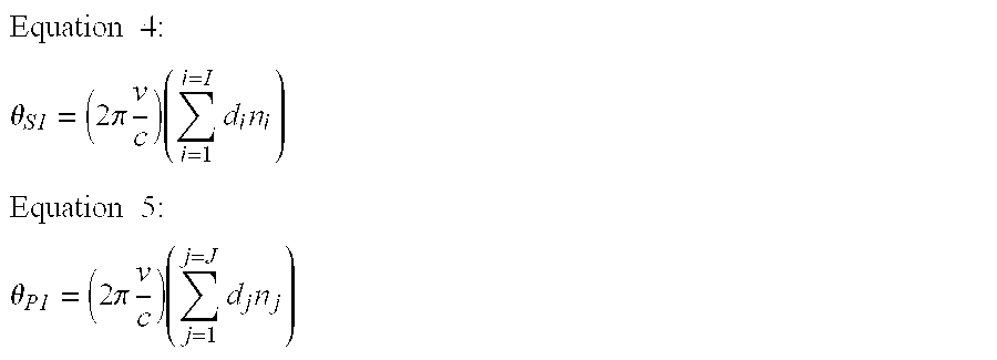
- where c and v are the frequency and velocity of light in free space and where I and J are the number of optical elements which make up the delay paths with delays θ S1 and θP1 respectively. For each of the i optical elements: vacuum, gas, plasma, liquid or solid which make up the delay path θS1, the ith element has a physical length di and an index of refraction ni. For each of the J optical elements: vacuum, gas, plasma, liquid or solid which make up the delay path θP1, the jth element has a physical length dj and an index of refraction nj. Optical elements include the optical coatings associated with polarization or intensity dependent beam splitters, which also contribute to optical pathlength and phase accumulations.
- The delay difference between the two paths is expressed in Equation 6.

- The delay difference for the cell is proportional to the difference in the optical path lengths between the S and P delay paths. Similar considerations apply in determining the delays and delay differences for the pair of delay paths in the
second cell 340. - The optical path length difference between the two delay paths in a cell corresponds inversely with the free spectral range (FSR) generated by the cell as evidenced in the orthogonal vector components of the output beam from the cell. This relationship is set forth in the following Equation 7.

- where L I and LJ are the total optical path length of the I and J elements which make up the corresponding delay paths θS and θP.
- For an optical interleaver the FSR should be a constant perhaps equal to the channel spacing between adjacent odd or even channels, e.g., 100 GHz. Using Equation 7 the delay difference required to generate this result can be determined, and from it a solution to the optical path lengths for each of the delay paths.
- FIG. 6E is a side elevation view of the variable coupling between cells of the multi-cell implementation shown in FIG. 6A. Coupling is used to control the amount an input of polarized light that will be projected onto the S and P delay paths of a corresponding cell. Three coupling views 660, 662 and 664 are shown at appropriate locations at the input to
cell 322, the interface betweencells cell 340 respectively. Only one ofbeams 542 on one of the optical processing legs, e. g. the first optical processing leg, are shown. The three views 660-664 are taken at the stated locations along the z-axis looking in the positive z direction along the propagation path of theinput beam 542. In the first of the coupling views 660, the polarized input is shown with a single input vector “I” and the orthogonal polarization axes PI and SI of thefirst cell 322 are shown. The input I may include orthogonal input vectors. The amount of light that is coupled onto either delay path in the first cell is determined by the angle φ1 of the incoming beam vector with the S polarization axis of the cell. In the example shown light frombeam 542 will couple to the P and S delay paths in amounts proportionate with the sin2(φ1) and the cos2(φ1) of the angle φ1 between the vector of the beam and the P and S axes. Rotation of the cell about the propagation path of thebeam 542 can be used to vary the coupling percentages or ratios between the incoming light and the P and S delay paths. In thenext coupling view 662, thebeam 546 fromcell 322 is coupled withcell 340. The orthogonal polarization vectors P1, S1 present in the output of thefundamental cell 322 are shown along with the orthogonal polarization vectors P2, S2 which are defined by the coupler of the next cell in the sequence, i.e.harmonic cell 340. The amount of light that is coupled onto either delay path in the second cell is determined by the angle φ2 between the two sets of orthogonal vectors forbeam 546 and the P and S axes ofcell 340. Thelast coupling view 664, shows both the orthogonal polarization vectors P2, S2 present in the output of the second cell along with a second set of orthogonal polarization vectors P0, S0. This last orthogonal vector set is used to represent the beam splitter/combiner/displacer 250 (see FIG. 3A) used to separate the orthogonal vectors within the single output beam into two discrete beams (not shown). The amount of light coupled onto the output beams is defined by the angle φ3 between the two sets of orthogonal vectors. - FIG. 6F shows the individual transforms associated with each of the four delay paths on one of the two optical processing legs through the two cell sequence shown in FIG. 6A. FIG. 6F shows the individual transforms 688 associated with each of the four distinct delay paths from the input of
beam 542 to the output ofbeam 546N. The number of discrete paths in a multi-cell sequence of N cells with two delay paths between each equals 2N. For two cells there are 22 or 4 discrete paths between an input and an output. The first of these paths is along delay paths θS1 and θS2 in thefirst cell 322 and thesecond cell 340 respectively. The second of these paths is along delay paths θS1 and θP2. The third of these paths is along delay paths θP1 and θS2. The fourth of these paths is along delay paths θP1 and θP2. The transfer function for the optical filter in single or sequential cell embodiments is the sum of the individual transfer functions associated with each discrete path from input to output. Transfer functions: 688, 690, 692, 694 are shown for the 1st to 4th paths discussed above. Each transfer function includes two terms 696-698. Thefirst term 696 corresponds to a coefficient in a Fourier series with the coefficient magnitude proportional to the product of the coupling or cross coupling coefficients along the particular path. Thesecond term 698 corresponds to the frequency component associated with that coefficient. The frequency component corresponds with the sum of the delays along a corresponding path. This in turn corresponds with the optical path lengths along each path. The sum of all the transfer functions forms a truncated Fourier series which fully defines the optical filter. - In an embodiment of the invention in which the optical telecommunications grid includes channels spaced apart by 50 GHz, a multi-cell design includes a fundamental cell of 100 GHz FSR and a harmonic cell of 50 GHz FSR to form polarization type square top comb filters. This filter can split an optical stream with 50 GHz channel spacing into two separate optical streams with odd and even 100 GHz channel spacing respectively or combine two optical streams with 100 GHz odd and even channel spacing respectively into a single optical stream with 50 GHz channel can spacing. The 1 st angle φ1 can be substantially equal to 45 degrees and the 2nd angle can be substantially equal to (45+15) degrees. Similarly, a first cell of 100 GHz FSR and a second cell of 50 GHz FSR can be used to form an intensity type of square top comb filters. The 1st splitting ratio substantially equals 50/50% and the 2nd splitting ratio substantially equals cos2(45°+15°)/sin2(45°+15°). In a multi-cell embodiment a square top filter function may be achieved by choosing one cell with the base FSR and remaining cells with FSRs of integer fractional multiples of the base FSR.
- Further teachings on sequentially coupled optical filter cells may be found in either of the two following references. See E. Harris et al., Optical Network Synthesis Using Birefringent Crystals, JOURNAL OF THE OPTICAL SOCIETY OF AMERICA, VOLUME 54,
Number 10, October 1964 for a general discussion of transfer functions related to birefringent crystals. See C. H. Henry et al. U.S. Pat. No. 5,596,661 entitled “Monolithic Optical Waveguide Filters based on Fourier Expansion” issued on Jan. 21, 1997 for a general discussion of transfer functions related to wave guides. - Passive Thermal Stabilization
- The typical application of optical filters constructed using the above techniques is an optical interleaver. In order for that interleaver to function properly it must create the desired stop bands and pass bands for the odd and even channels which it separates. For current telecommunication applications the filter would be designed with a constant FSR perhaps equal to the channel spacing, i.e., 100 GHz. An optical filter with this FSR would generate the required stop bands and pass bands in each of the orthogonal polarization vectors present on the output. One of the orthogonal output vectors would contain the pass bands associated with the center wavelengths of the odd channels. The other of the orthogonal output vectors would contain the pass bands associated with the center wavelengths of the even channels.
- Temperature variations in a interleaver that may effect the performance may result from the environment or from the power transmitted through the interleaver. This can result in the periodic odd and even pass bands generated by the optical filter moving out of alignment with the selected grid, i.e., the ITU grid. This is primarily because the center wavelength of a pass band slips with temperature. This misalignment results in attenuation of signal strength, cross talk and ultimately loss of transmission/reception capability until the optical filter returns to its original temperature. In practice therefore, the optical filters and interleavers fabricated there from must be thermally stable across a range of temperatures.
- One solution is to flatten the pass bands of the filter. Multi cell filter designs such as those discussed above allow the pass bands to exhibit higher order harmonics in the form of non-sinusoidal pass band profiles, a.k.a. “flat tops” (see FIG. 11). The close spacing between the channels in a WDM makes it desirable to design a WDM with flat pass bands in order to increase the error tolerance to temperature induced shifts in the pass bands. Even with flat top filter profiles, however, temperature stabilization is still required due to the precise telecommunication channel spacing.
- A further solution is to actively stabilize the temperature of the interleaver using a heater or cooler and a closed loop feedback of temperature or wavelength. This solution can be expensive and may increase the form factor of the interleaver. Nevertheless, the current invention may be practiced with active temperature stabilization. A possible benefit to active temperature stabilization is that the optical elements which make up each pair of delay paths may all be fabricated from a common medium with identical indices of refraction and thermal expansion coefficient.
- Although capable of being utilized in systems with active temperature stabilization, the current invention is capable of providing temperature stability for the optical filters without active temperature control where appropriate. This greatly enhances the precision of the interleavers or systems fabricated there from and reduces system cost. The current invention is capable of providing passive temperature stabilization of an optical interleaver, through proper selection and design of the optical elements which form each pair of delay paths so that the delay difference for each pair of delay paths and hence the system as a whole remain constant. Since the delay difference is directly related to the difference in the optical path lengths this invention provides thermal stabilization of the delay difference. In an embodiment of the invention either the birefringent or the polarization beam splitting filters may be fabricated with at least one of the delay paths having two optical elements, each of which exhibits a different optical path length response to temperature. Typically, this takes the form of optical elements with different thermal optic coefficients.
- The system is designed so that d(L 1−Lj)/dT equals substantially zero. This latter condition is satisfied when the derivative of the denominator in Equation 7 substantially equals zero as set forth in the following Equation 8:

- where α j and αj are the thermal expansion coefficients for each optical element which form the S and P delay paths respectively in each cell and where βj and βj are the thermal optic coefficients for the temperature induced change in the refractive index for each element in the S and P delay paths respectively.
- The following Table 1 shows various relevant optical parameters for some optical media which may be used to fabricate the optical elements which make up each pair of delay paths.
TABLE 1 @1550 nm Vacuum Air BK7 SF5 Fused Silica BaK1 LaSFN3 n 1 1.00027 1.50066 1.64329 1.4409 1.55517 1.77448 
0 0* 0.907465 1.407 13.7 0.066 2.293 α × 10−6 0 0* 5.1 8.2 0.052 7.6 6.2 - The second row sets forth each material's refractive index at 1550 nm. The change in refractive index n as a function of temperature β is set forth in the third row. Row 4 sets forth the coefficient of thermal expansion α for the medium. The selection of physical length of each optical component can be determined by solving
Equation 4 and 5 together. - Further passive thermal stabilization may be achieved by horizontally mounting a polarization beam splitting cell to a substrate as illustrated in FIG. 5N.
- FIGS. 7A-B are graphs showing the complementary dispersion profiles about a representative center frequency of one of the channels for an optical interleaver fabricated in accordance with the current invention. The complementary dispersion profiles result from the above discussed asymmetry in the fundamental filter between the optical pathlengths along the portions of the first and second legs of the optical loop which intersect the fundamental filter. FIG. 7A shows a representative dispersion profile where coupling of light onto fast and slow paths of either of the optical processing legs is in equal proportions. The dispersion profiles 700 and 702 for the first leg and the second leg are shown relative to the substantially flat line
composite dispersion 704. The flat line dispersion profile results from the broadband phase shift for the odd and even channel sets between the first and second optical processing legs in the fundamental filter cell. This phase shift of odd integer multiples of substantially half a wavelength for each center wavelength of a corresponding channel in both the odd set of channels and the even set of channels causes the odd channel set and the even channel set to experience the fundamental filter cell as respectively a full/half waveplate and a half/full waveplate on the first and second legs of the optical loop within the fundamental filter cell. This phase shift is advantageous because it improves the signal integrity associated with multiplexing and de-multiplexing telecom communications by reducing overall chromatic dispersion in each of the channels filtered by the interleaver. - FIG. 7B shows a representative dispersion profile where coupling of light onto fast and slow paths of either of the optical processing legs is in un-equal proportions. The dispersion profiles 710 and 714 for the first and second leg of the optical loop are shown relative to the
composite dispersion 716. The composite dispersion exhibits some deviation from the desired flat line response, but the tradeoff in terms of enhanced stop bands in the filter transform is appropriate for some applications as will be shown in the following FIGS. 8A-E - FIGS. 8A-E are signal diagrams showing filter functions at various locations along the optical path of the interleaver shown in FIGS. 1-6. The signal diagrams shown in FIGS. 8A-B show the periodic comb filter functions to which the even channels are exposed on the first and second legs of the optical processing loop respectively. The first comb filter function to which the even channels are exposed on the first leg includes pass bands for the even channels interlaced with residual components, or bleed through, of the odd channels and is shown in FIG. 8A. In the first leg, in this example the even channels are subject to a phase retardation substantially equal to the incident wavelength or integer multiples thereof. Thus there is a
pass band 860 forchannel 10 and one forchannel 12. Thecenter frequency 864 for the pass band forchannel 12 coincides with a selected order of the incident wavelength, e.g.,order 3875. Between the pass bands for the even channels there is a bleed through of the odd pass bands below the −10 dB level. The bleed through 862 forchannel 11, as well aschannels - The coupling asymmetries in the first leg between the fast and slow paths of each filter cell are present in the second leg as shown for the even channels in FIG. 8B. Because of the wavelength shift of λ/2 or odd integer multiples thereof, in the optical pathlength difference between the portion of the first and second legs which intersect the fundamental cell, the even channels are subject to a second comb filter function different than that to which they were exposed in the first sub-stage. This second comb filter function shown in FIG. 8B includes narrow stop bands, and substantially attenuated bleed-through of the odd channels. There is a
pass band 866 forchannel 10 and one forchannel 12 with a slight dip in the flat top. Thecenter frequency 864 forchannel 12 coincides with a different selected order of the incident wavelength,e.g. order 3876, than was the case in the filter of the first sub-stage as shown in FIG. 8A. - The signal diagrams shown in FIGS. 8C-D show the comb filter functions to which the odd channels are exposed on the first and second legs of the optical processing loop respectively. In the first leg, in this example the odd channels are subject to the second comb filter function with a wavelength shift of λ/2 or odd integer multiples thereof. Thus there is a
pass band 870 forchannel 11 and one forchannels center frequency 864 for the pass band forchannel 12 coincides with a selected order of the incident wavelength,e.g. order 3875. The filter function for the odd channels in the first sub-stage exhibits narrow stop bands, and substantially attenuated bleed-through. The coupling asymmetries in the first leg between the fast and slow paths of each filter cell are present in the second leg. - As show in FIG. 8D the wavelength shift of λ/2 in the optical pathlength difference between the portion of the first and second legs which intersects the fundamental cell results in the odd channels also being subject to a different, i.e. complementary filter function, to that experienced in the first leg. The odd channels are exposed to the first comb filter function with a wavelength shift of λ/2 or odd integer multiples thereof. There is a
pass band 874 forchannel 11 and one forchannels channel 10, as well aschannel 12 is shown. This bleed through results from asymmetric coupling of light onto the fast and slow paths in amounts other than 50%/50%. The same coupling ratios used in the first leg are applied in the second leg. Thecenter frequency 864 for the pass band forchannel 12 coincides with a different selected order of the incident wavelength,e.g. order 3876, than was the case in the fundamental filter on the first leg as shown in FIG. 8C. - FIG. 8E shows the composite performance for the interleaver for both the odd and even channels. The
pass band 810 for evenchannel 10 as well as forchannel 12 is shown. Thepass band 812 forodd channel 11 as well as forchannels 9 13 are also shown. Each pass band exhibits steep side profiles and broad stop bands when compared with prior art designs. Thepass band 812 forchannel 11 is shown with a broad flat top 804 and withbroad pass bands pass band 812 is askirt 820 representative of traditional pass band profiles. By comparison the current interleaver exhibits a significant improvement in the pass band profiles it generates with relatively steeper sides and broader stop bands. These improvements translate into increases in the signal integrity of the telecommunications data handled by the interleaver. - In alternate embodiments of the invention, the various filter, retro reflector and other elements of the optical interleaver may be fabricated on a common semi-conductor substrate. The various components: reflectors, couplers, and optical elements may be fabricated using a combination of etching and deposition techniques well know in the semi-conductor industry.
- The foregoing description of preferred embodiments of the invention has been presented for purposes of illustration and description. It is not intended to be exhaustive or to limit the invention to the precise forms disclosed. Obviously many modifications and variations will be apparent to practitioners skilled in this art.
Claims (20)
1. A hermetically sealed collimator, comprising:
a collimator tube for hermetically sealing a collimator to an optical device;
a lens soldered within the collimator tube to form a hermetic seal between the lens and the collimator tube; and
a ferrule within the collimator tube for directing one or more optical fibers to the lens and holding the one or more optical fibers within the collimator tube.
2. A hermetically sealed collimator as recited in claim 1 , wherein the lens is hermetically sealed directly to the collimator tube.
3. A hermetically sealed collimator as recited in claim 1 , wherein the lens is hermetically sealed indirectly to the collimator tube through a lens housing.
4. A hermetically sealed collimator as recited in claim 3 , wherein the lens housing and the collimator tube are gold plated at the points where they are soldered together.
5. A hermetically sealed collimator as recited in claim 1 , wherein at least a portion of the collimator tube is gold plated so that the collimator tube can be soldered to an optical device and form a hermetic seal.
6. A hermetically sealed collimator as recited in claim 1 , wherein the hermetically sealed collimator is hermetically sealed to an optical interleaver.
7. A hermetically sealed collimator as recited in claim 1 , wherein the collimator tube diameter is based on the lens diameter.
8. A hermetically sealed collimator, comprising:
a collimator tube for hermetically sealing a collimator to an optical device;
a lens housing soldered within the collimator tube to form a hermetic seal between the lens housing and the collimator tube;
a lens soldered to the lens housing in order to form a hermetic seal between the lens and the lens housing; and
a ferrule within the collimator tube for directing one or more optical fibers to the lens and holding the one or more optical fibers within the collimator tube.
9. A hermetically sealed collimator as recited in claim 8 , wherein the lens housing and the collimator tube are gold plated at the points where they are soldered together in order to form a hermetic seal.
10. A hermetically sealed collimator as recited in claim 8 , wherein at least a portion of the collimator tube is gold plated so that the collimator tube can be soldered to an optical device and form a hermetic seal.
11. A hermetically sealed collimator as recited in claim 8 , wherein the collimator tube diameter is based on the lens diameter.
12. A hermetically sealed collimator as recited in claim 8 , wherein the hermetically sealed collimator is hermetically sealed to an optical interleaver.
13. An optical interleaver for processing optical signals including a first set of one or more optical signals and a second set of one or more optical signals, the interleaver comprising:
a fundamental filter cell for filtering optical signal propagating on each of two legs of an optical loop, the fundamental filter cell operating as a full waveplate to a first set of one or more optical signals and as a half waveplate to a second set of one or more optical signals one of the two processing legs, and as a half waveplate to the first set of one or more optical signals and as a full waveplate to the second set of one or more optical signals on another of the two processing legs;
a retro-reflector optically coupled with the fundamental filter cell to reflect the optical signals from one of the two processing legs to the other of the two processing legs in order to form the optical loop;
a displacer optically coupled between the fundamental filter cell and the retro reflector to split or combine the first set of one or more optical signals and the second set of one or more optical signals depending on polarization and propagation direction along the optical loop; and
three hermetically sealed collimators that are hermetically sealed to the optical interleaver, each hermetically sealed collimator comprising a lens hermetically sealed to a corresponding collimator tube.
14. An optical interleaver as recited in claim 13 , wherein each lens is hermetically sealed directly to its corresponding collimator tube.
15. An optical interleaver as recited in claim 14 , wherein each lens and each collimator tube are soldered together to form a hermetic seal, and wherein each lens and each collimator tube are gold plated at the points where they soldered together.
16. An optical interleaver as recited in claim 13 , wherein each lens is hermetically sealed indirectly to its corresponding collimator tube through a lens housing.
17. An optical interleaver as recited in claim 16 , wherein each lens, lens housing, and collimator tube are soldered together to form a hermetic seal, and wherein each lens housing and each collimator tube are gold plated at the points where they are soldered together.
18. An optical interleaver as recited in claim 13 , wherein each hermetically sealed collimator further comprises a ferrule within the corresponding collimator tube for directing one or more optical fibers to the lens and holding the one or more optical fibers within the corresponding collimator tube.
19. An optical interleaver as recited in claim 13 , wherein each collimator tube diameter is based on the corresponding lens diameter.
20. An optical interleaver as recited in claim 13 , wherein the three hermetically sealed collimators comprise a first collimator for the first set of one or more optical signals, a second collimator the second set of one or more optical signals, and a third collimator for a combination of the first and second sets of one or more optical signals.
Priority Applications (1)
| Application Number | Priority Date | Filing Date | Title |
|---|---|---|---|
| US10/866,550 US20040223222A1 (en) | 2002-06-12 | 2004-06-11 | Hermetically sealed collimator and optical interleaver design |
Applications Claiming Priority (2)
| Application Number | Priority Date | Filing Date | Title |
|---|---|---|---|
| US10/170,055 US6850364B2 (en) | 2002-06-12 | 2002-06-12 | Method and apparatus for an optical multiplexer and demultiplexer with an optical processing loop |
| US10/866,550 US20040223222A1 (en) | 2002-06-12 | 2004-06-11 | Hermetically sealed collimator and optical interleaver design |
Related Parent Applications (1)
| Application Number | Title | Priority Date | Filing Date |
|---|---|---|---|
| US10/170,055 Continuation-In-Part US6850364B2 (en) | 2002-06-12 | 2002-06-12 | Method and apparatus for an optical multiplexer and demultiplexer with an optical processing loop |
Publications (1)
| Publication Number | Publication Date |
|---|---|
| US20040223222A1 true US20040223222A1 (en) | 2004-11-11 |
Family
ID=46205258
Family Applications (1)
| Application Number | Title | Priority Date | Filing Date |
|---|---|---|---|
| US10/866,550 Abandoned US20040223222A1 (en) | 2002-06-12 | 2004-06-11 | Hermetically sealed collimator and optical interleaver design |
Country Status (1)
| Country | Link |
|---|---|
| US (1) | US20040223222A1 (en) |
Cited By (2)
| Publication number | Priority date | Publication date | Assignee | Title |
|---|---|---|---|---|
| US7768708B1 (en) | 2006-02-03 | 2010-08-03 | Raytheon Company | Light source having spatially interleaved light beams |
| WO2018013709A1 (en) * | 2016-07-13 | 2018-01-18 | Micatu Inc. | An integrated polarizing and analyzing optical fiber collimator device and methods of use thereof |
Citations (21)
| Publication number | Priority date | Publication date | Assignee | Title |
|---|---|---|---|---|
| US4094581A (en) * | 1977-01-31 | 1978-06-13 | Westinghouse Electric Corp. | Electro-optic modulator with compensation of thermally induced birefringence |
| US4685773A (en) * | 1984-09-13 | 1987-08-11 | Gte Laboratories Incorporated | Birefringent optical multiplexer with flattened bandpass |
| US4813761A (en) * | 1987-11-16 | 1989-03-21 | Davis Jeffrey A | High efficiency spatial masks |
| US4987567A (en) * | 1988-11-21 | 1991-01-22 | Gte Laboratories Incorporated | Optical wavelength multiplexer/demultiplexer and demultiplexer/remultiplexer |
| US5210815A (en) * | 1992-04-09 | 1993-05-11 | G & H Technology, Inc. | Hermetically sealed optical fiber feedthrough |
| US5596661A (en) * | 1994-12-28 | 1997-01-21 | Lucent Technologies Inc. | Monolithic optical waveguide filters based on Fourier expansion |
| US5606439A (en) * | 1996-04-10 | 1997-02-25 | Macro-Vision Technology , Inc. | Tunable add/drop optical filter |
| US5694205A (en) * | 1995-10-19 | 1997-12-02 | Alliedsignal Inc. | Birefringent-biased sensor having temperature compensation |
| US5694233A (en) * | 1996-07-23 | 1997-12-02 | Macro-Vision Communications, Llc | Switchable wavelength router |
| US5867291A (en) * | 1996-10-29 | 1999-02-02 | Chorum Technologies Inc. | Programmable wavelength router |
| US6005697A (en) * | 1996-07-23 | 1999-12-21 | Macro-Vision Communications, L.L.C. | Multi-wavelength cross-connect optical network |
| US6040932A (en) * | 1997-04-25 | 2000-03-21 | Duck; Gary S. | Method and circuit for demultiplexing an optical signal |
| US6142678A (en) * | 1999-06-15 | 2000-11-07 | Jds Uniphase Inc. | Optical coupling |
| US6208444B1 (en) * | 1996-10-29 | 2001-03-27 | Chorum Technologies Inc. | Apparatus for wavelength demultiplexing using a multi-cavity etalon |
| US6212313B1 (en) * | 2000-01-31 | 2001-04-03 | Oplink Communications, Inc. | Optical interleaver |
| US6373604B1 (en) * | 1999-10-01 | 2002-04-16 | New Focus, Inc. | Optical MUX/DEMUX |
| US20020097957A1 (en) * | 2001-01-22 | 2002-07-25 | Juro Kikuchi | Arrayed optical device |
| US6631220B1 (en) * | 2000-07-07 | 2003-10-07 | Optiwork, Inc. | Optical isolator |
| US6681473B1 (en) * | 2002-02-15 | 2004-01-27 | Calient Networks, Inc. | Method and apparatus for hermetically sealing fiber array blocks |
| US6714703B2 (en) * | 2001-11-21 | 2004-03-30 | Hon Hai Precision Ind. Co., Ltd. | Optical collimator and method for making same |
| US6795182B2 (en) * | 2001-07-06 | 2004-09-21 | Arroyo Optics, Inc. | Diffractive fourier optics for optical communications |
-
2004
- 2004-06-11 US US10/866,550 patent/US20040223222A1/en not_active Abandoned
Patent Citations (21)
| Publication number | Priority date | Publication date | Assignee | Title |
|---|---|---|---|---|
| US4094581A (en) * | 1977-01-31 | 1978-06-13 | Westinghouse Electric Corp. | Electro-optic modulator with compensation of thermally induced birefringence |
| US4685773A (en) * | 1984-09-13 | 1987-08-11 | Gte Laboratories Incorporated | Birefringent optical multiplexer with flattened bandpass |
| US4813761A (en) * | 1987-11-16 | 1989-03-21 | Davis Jeffrey A | High efficiency spatial masks |
| US4987567A (en) * | 1988-11-21 | 1991-01-22 | Gte Laboratories Incorporated | Optical wavelength multiplexer/demultiplexer and demultiplexer/remultiplexer |
| US5210815A (en) * | 1992-04-09 | 1993-05-11 | G & H Technology, Inc. | Hermetically sealed optical fiber feedthrough |
| US5596661A (en) * | 1994-12-28 | 1997-01-21 | Lucent Technologies Inc. | Monolithic optical waveguide filters based on Fourier expansion |
| US5694205A (en) * | 1995-10-19 | 1997-12-02 | Alliedsignal Inc. | Birefringent-biased sensor having temperature compensation |
| US5606439A (en) * | 1996-04-10 | 1997-02-25 | Macro-Vision Technology , Inc. | Tunable add/drop optical filter |
| US6005697A (en) * | 1996-07-23 | 1999-12-21 | Macro-Vision Communications, L.L.C. | Multi-wavelength cross-connect optical network |
| US5694233A (en) * | 1996-07-23 | 1997-12-02 | Macro-Vision Communications, Llc | Switchable wavelength router |
| US5867291A (en) * | 1996-10-29 | 1999-02-02 | Chorum Technologies Inc. | Programmable wavelength router |
| US6208444B1 (en) * | 1996-10-29 | 2001-03-27 | Chorum Technologies Inc. | Apparatus for wavelength demultiplexing using a multi-cavity etalon |
| US6040932A (en) * | 1997-04-25 | 2000-03-21 | Duck; Gary S. | Method and circuit for demultiplexing an optical signal |
| US6142678A (en) * | 1999-06-15 | 2000-11-07 | Jds Uniphase Inc. | Optical coupling |
| US6373604B1 (en) * | 1999-10-01 | 2002-04-16 | New Focus, Inc. | Optical MUX/DEMUX |
| US6212313B1 (en) * | 2000-01-31 | 2001-04-03 | Oplink Communications, Inc. | Optical interleaver |
| US6631220B1 (en) * | 2000-07-07 | 2003-10-07 | Optiwork, Inc. | Optical isolator |
| US20020097957A1 (en) * | 2001-01-22 | 2002-07-25 | Juro Kikuchi | Arrayed optical device |
| US6795182B2 (en) * | 2001-07-06 | 2004-09-21 | Arroyo Optics, Inc. | Diffractive fourier optics for optical communications |
| US6714703B2 (en) * | 2001-11-21 | 2004-03-30 | Hon Hai Precision Ind. Co., Ltd. | Optical collimator and method for making same |
| US6681473B1 (en) * | 2002-02-15 | 2004-01-27 | Calient Networks, Inc. | Method and apparatus for hermetically sealing fiber array blocks |
Cited By (4)
| Publication number | Priority date | Publication date | Assignee | Title |
|---|---|---|---|---|
| US7768708B1 (en) | 2006-02-03 | 2010-08-03 | Raytheon Company | Light source having spatially interleaved light beams |
| WO2018013709A1 (en) * | 2016-07-13 | 2018-01-18 | Micatu Inc. | An integrated polarizing and analyzing optical fiber collimator device and methods of use thereof |
| US20180017734A1 (en) * | 2016-07-13 | 2018-01-18 | Micatu Inc. | Integrated polarizing and analyzing optical fiber collimator device and methods of use thereof |
| US10175425B2 (en) | 2016-07-13 | 2019-01-08 | Micatu Inc. | Integrated polarizing and analyzing optical fiber collimator device and methods of use thereof |
Similar Documents
| Publication | Publication Date | Title |
|---|---|---|
| US6455841B2 (en) | Optical wavelength router based on polarization interferometer | |
| US6498680B1 (en) | Compact tunable optical wavelength interleaver | |
| US6867868B1 (en) | Method and apparatus for tunable interferometer utilizing variable air density | |
| US6275322B1 (en) | Michelson phase shifter interleaver/deinterleavers | |
| US6674968B1 (en) | Passive thermal stabilization for an optical mux/demux | |
| US6690846B2 (en) | Dispersion-compensated optical wavelength router | |
| US7173763B2 (en) | Optical interleaver and filter cell design with enhanced clear aperture | |
| US6765679B2 (en) | Multi-cavity interferometer with dispersion compensating resonators | |
| US6694066B2 (en) | Method and apparatus for an optical filter | |
| US6907167B2 (en) | Optical interleaving with enhanced spectral response and reduced polarization sensitivity | |
| US6684002B2 (en) | Method and apparatus for an optical filter | |
| US6909511B2 (en) | Athermal interferometer | |
| US6850364B2 (en) | Method and apparatus for an optical multiplexer and demultiplexer with an optical processing loop | |
| US20020085252A1 (en) | Interleaver filters employing non-birefringent elements | |
| US20040190906A1 (en) | Method and apparatus for simultaneous optical compensation of chromatic and polarization mode dispersion | |
| US7268944B2 (en) | Optical interleaver, filter cell, and component design with reduced chromatic dispersion | |
| US7106508B2 (en) | Hybrid cell | |
| US20040223222A1 (en) | Hermetically sealed collimator and optical interleaver design | |
| CN100559745C (en) | Be used to handle the device of light signal | |
| US6643063B2 (en) | Deinterleaver with high isolation and dispersion compensation and 50/200GHz interleaver and deinterleaver | |
| US20020196540A1 (en) | Interleaver having Gires-Tournois resonator | |
| US20040227996A1 (en) | Optical interleaver and filter cell design with enhanced thermal stability | |
| EP1163751B1 (en) | Otpical mux/demux | |
| US20020094157A1 (en) | Polarization dependent filtering device utilizing a fabry-perot cavity |
Legal Events
| Date | Code | Title | Description |
|---|---|---|---|
| AS | Assignment |
Owner name: FINISAR CORPORATION, UTAH Free format text: ASSIGNMENT OF ASSIGNORS INTEREST;ASSIGNORS:SCHOTT, DANIEL PHILIP;DU, TENGDA;LUO, XIN;AND OTHERS;REEL/FRAME:015464/0395;SIGNING DATES FROM 20040610 TO 20040611 |
|
| STCB | Information on status: application discontinuation |
Free format text: ABANDONED -- FAILURE TO RESPOND TO AN OFFICE ACTION |
|
| AS | Assignment |
Owner name: II-VI DELAWARE, INC., DELAWARE Free format text: ASSIGNMENT OF ASSIGNORS INTEREST;ASSIGNOR:FINISAR CORPORATION;REEL/FRAME:052286/0001 Effective date: 20190924 |