US20040183066A1 - P-type materials and mixtures for electronic devices - Google Patents
P-type materials and mixtures for electronic devices Download PDFInfo
- Publication number
- US20040183066A1 US20040183066A1 US10/391,176 US39117603A US2004183066A1 US 20040183066 A1 US20040183066 A1 US 20040183066A1 US 39117603 A US39117603 A US 39117603A US 2004183066 A1 US2004183066 A1 US 2004183066A1
- Authority
- US
- United States
- Prior art keywords
- organic
- carbon atoms
- substituted
- heterocyclic
- aryl
- Prior art date
- Legal status (The legal status is an assumption and is not a legal conclusion. Google has not performed a legal analysis and makes no representation as to the accuracy of the status listed.)
- Granted
Links
- 239000000203 mixture Substances 0.000 title claims abstract description 27
- 239000000463 material Substances 0.000 title claims description 89
- 239000002019 doping agent Substances 0.000 claims abstract description 44
- -1 dihydrophenazine compound Chemical class 0.000 claims abstract description 36
- 125000004432 carbon atom Chemical group C* 0.000 claims description 44
- 125000000623 heterocyclic group Chemical group 0.000 claims description 44
- 125000004122 cyclic group Chemical group 0.000 claims description 39
- 125000003118 aryl group Chemical group 0.000 claims description 25
- 239000001257 hydrogen Substances 0.000 claims description 23
- 229910052739 hydrogen Inorganic materials 0.000 claims description 23
- 125000003342 alkenyl group Chemical group 0.000 claims description 21
- 125000000217 alkyl group Chemical group 0.000 claims description 21
- 125000005017 substituted alkenyl group Chemical group 0.000 claims description 21
- 125000003107 substituted aryl group Chemical group 0.000 claims description 21
- 125000003545 alkoxy group Chemical group 0.000 claims description 18
- 125000004104 aryloxy group Chemical group 0.000 claims description 18
- 229910052736 halogen Inorganic materials 0.000 claims description 18
- 150000002367 halogens Chemical group 0.000 claims description 18
- 125000002924 primary amino group Chemical group [H]N([H])* 0.000 claims description 18
- 125000004001 thioalkyl group Chemical group 0.000 claims description 6
- 125000005000 thioaryl group Chemical group 0.000 claims description 6
- RBTARNINKXHZNM-UHFFFAOYSA-K iron trichloride Chemical compound Cl[Fe](Cl)Cl RBTARNINKXHZNM-UHFFFAOYSA-K 0.000 claims description 4
- ZIZMDHZLHJBNSQ-UHFFFAOYSA-N 1,2-dihydrophenazine Chemical compound C1=CC=C2N=C(C=CCC3)C3=NC2=C1 ZIZMDHZLHJBNSQ-UHFFFAOYSA-N 0.000 claims description 3
- 229910021578 Iron(III) chloride Inorganic materials 0.000 claims description 3
- VMPVEPPRYRXYNP-UHFFFAOYSA-I antimony(5+);pentachloride Chemical compound Cl[Sb](Cl)(Cl)(Cl)Cl VMPVEPPRYRXYNP-UHFFFAOYSA-I 0.000 claims description 3
- SHXXPRJOPFJRHA-UHFFFAOYSA-K iron(iii) fluoride Chemical compound F[Fe](F)F SHXXPRJOPFJRHA-UHFFFAOYSA-K 0.000 claims description 3
- 125000004435 hydrogen atom Chemical group [H]* 0.000 claims 7
- ZCYVEMRRCGMTRW-UHFFFAOYSA-N 7553-56-2 Chemical compound [I] ZCYVEMRRCGMTRW-UHFFFAOYSA-N 0.000 claims 1
- 229910052740 iodine Inorganic materials 0.000 claims 1
- 239000011630 iodine Substances 0.000 claims 1
- 239000010410 layer Substances 0.000 description 87
- YXFVVABEGXRONW-UHFFFAOYSA-N Toluene Chemical compound CC1=CC=CC=C1 YXFVVABEGXRONW-UHFFFAOYSA-N 0.000 description 57
- 150000001875 compounds Chemical class 0.000 description 45
- 239000012044 organic layer Substances 0.000 description 44
- 238000000034 method Methods 0.000 description 26
- 230000015572 biosynthetic process Effects 0.000 description 19
- MFRIHAYPQRLWNB-UHFFFAOYSA-N sodium tert-butoxide Chemical compound [Na+].CC(C)(C)[O-] MFRIHAYPQRLWNB-UHFFFAOYSA-N 0.000 description 18
- 239000011777 magnesium Substances 0.000 description 16
- BWHDROKFUHTORW-UHFFFAOYSA-N tritert-butylphosphane Chemical compound CC(C)(C)P(C(C)(C)C)C(C)(C)C BWHDROKFUHTORW-UHFFFAOYSA-N 0.000 description 16
- KDLHZDBZIXYQEI-UHFFFAOYSA-N Palladium Chemical compound [Pd] KDLHZDBZIXYQEI-UHFFFAOYSA-N 0.000 description 15
- 229910052751 metal Inorganic materials 0.000 description 15
- 239000002184 metal Substances 0.000 description 15
- 239000004065 semiconductor Substances 0.000 description 15
- 239000007787 solid Substances 0.000 description 15
- 238000003786 synthesis reaction Methods 0.000 description 15
- 150000002431 hydrogen Chemical group 0.000 description 14
- 239000000758 substrate Substances 0.000 description 14
- 238000002347 injection Methods 0.000 description 13
- 239000007924 injection Substances 0.000 description 13
- IXHWGNYCZPISET-UHFFFAOYSA-N 2-[4-(dicyanomethylidene)-2,3,5,6-tetrafluorocyclohexa-2,5-dien-1-ylidene]propanedinitrile Chemical compound FC1=C(F)C(=C(C#N)C#N)C(F)=C(F)C1=C(C#N)C#N IXHWGNYCZPISET-UHFFFAOYSA-N 0.000 description 12
- 238000000151 deposition Methods 0.000 description 12
- 230000008021 deposition Effects 0.000 description 12
- MCJGNVYPOGVAJF-UHFFFAOYSA-N quinolin-8-ol Chemical compound C1=CN=C2C(O)=CC=CC2=C1 MCJGNVYPOGVAJF-UHFFFAOYSA-N 0.000 description 12
- VLKZOEOYAKHREP-UHFFFAOYSA-N n-Hexane Chemical class CCCCCC VLKZOEOYAKHREP-UHFFFAOYSA-N 0.000 description 11
- 239000000047 product Substances 0.000 description 10
- 238000000859 sublimation Methods 0.000 description 10
- 230000008022 sublimation Effects 0.000 description 10
- 238000010626 work up procedure Methods 0.000 description 10
- 239000004020 conductor Substances 0.000 description 9
- 230000003287 optical effect Effects 0.000 description 9
- 238000012546 transfer Methods 0.000 description 9
- YMWUJEATGCHHMB-UHFFFAOYSA-N Dichloromethane Chemical compound ClCCl YMWUJEATGCHHMB-UHFFFAOYSA-N 0.000 description 8
- LFQSCWFLJHTTHZ-UHFFFAOYSA-N Ethanol Chemical compound CCO LFQSCWFLJHTTHZ-UHFFFAOYSA-N 0.000 description 8
- NZYXEOYGRPZMDP-UHFFFAOYSA-N 2,3-dimethyl-5,12-dihydrobenzo[b]phenazine Chemical compound C1=CC=C2C=C(NC3=C(C=C(C(=C3)C)C)N3)C3=CC2=C1 NZYXEOYGRPZMDP-UHFFFAOYSA-N 0.000 description 7
- 238000000434 field desorption mass spectrometry Methods 0.000 description 7
- 239000011521 glass Substances 0.000 description 7
- 239000011368 organic material Substances 0.000 description 7
- 239000000126 substance Substances 0.000 description 7
- VEPOHXYIFQMVHW-XOZOLZJESA-N 2,3-dihydroxybutanedioic acid (2S,3S)-3,4-dimethyl-2-phenylmorpholine Chemical compound OC(C(O)C(O)=O)C(O)=O.C[C@H]1[C@@H](OCCN1C)c1ccccc1 VEPOHXYIFQMVHW-XOZOLZJESA-N 0.000 description 6
- JLTDJTHDQAWBAV-UHFFFAOYSA-N N,N-dimethylaniline Chemical compound CN(C)C1=CC=CC=C1 JLTDJTHDQAWBAV-UHFFFAOYSA-N 0.000 description 6
- IMNFDUFMRHMDMM-UHFFFAOYSA-N N-Heptane Chemical compound CCCCCCC IMNFDUFMRHMDMM-UHFFFAOYSA-N 0.000 description 6
- 238000006243 chemical reaction Methods 0.000 description 6
- 238000010276 construction Methods 0.000 description 6
- JRNGUTKWMSBIBF-UHFFFAOYSA-N naphthalene-2,3-diol Chemical compound C1=CC=C2C=C(O)C(O)=CC2=C1 JRNGUTKWMSBIBF-UHFFFAOYSA-N 0.000 description 6
- 239000007983 Tris buffer Substances 0.000 description 5
- 150000004982 aromatic amines Chemical class 0.000 description 5
- 239000010406 cathode material Substances 0.000 description 5
- 230000000052 comparative effect Effects 0.000 description 5
- 238000009792 diffusion process Methods 0.000 description 5
- 238000005401 electroluminescence Methods 0.000 description 5
- 229910052744 lithium Inorganic materials 0.000 description 5
- 229910052749 magnesium Inorganic materials 0.000 description 5
- 229960003540 oxyquinoline Drugs 0.000 description 5
- 150000003384 small molecules Chemical class 0.000 description 5
- 238000002207 thermal evaporation Methods 0.000 description 5
- 125000005259 triarylamine group Chemical group 0.000 description 5
- IYZMXHQDXZKNCY-UHFFFAOYSA-N 1-n,1-n-diphenyl-4-n,4-n-bis[4-(n-phenylanilino)phenyl]benzene-1,4-diamine Chemical compound C1=CC=CC=C1N(C=1C=CC(=CC=1)N(C=1C=CC(=CC=1)N(C=1C=CC=CC=1)C=1C=CC=CC=1)C=1C=CC(=CC=1)N(C=1C=CC=CC=1)C=1C=CC=CC=1)C1=CC=CC=C1 IYZMXHQDXZKNCY-UHFFFAOYSA-N 0.000 description 4
- OOVVBDPQJDURKE-UHFFFAOYSA-N 5,12-dihydrobenzo[b]phenazine Chemical compound C1=CC=C2C=C3NC4=CC=CC=C4NC3=CC2=C1 OOVVBDPQJDURKE-UHFFFAOYSA-N 0.000 description 4
- GYHNNYVSQQEPJS-UHFFFAOYSA-N Gallium Chemical compound [Ga] GYHNNYVSQQEPJS-UHFFFAOYSA-N 0.000 description 4
- 229910052782 aluminium Inorganic materials 0.000 description 4
- XAGFODPZIPBFFR-UHFFFAOYSA-N aluminium Chemical compound [Al] XAGFODPZIPBFFR-UHFFFAOYSA-N 0.000 description 4
- 239000002800 charge carrier Substances 0.000 description 4
- 238000001816 cooling Methods 0.000 description 4
- 238000005538 encapsulation Methods 0.000 description 4
- 229910052733 gallium Inorganic materials 0.000 description 4
- 239000000543 intermediate Substances 0.000 description 4
- 150000002739 metals Chemical class 0.000 description 4
- 239000012299 nitrogen atmosphere Substances 0.000 description 4
- BASFCYQUMIYNBI-UHFFFAOYSA-N platinum Chemical compound [Pt] BASFCYQUMIYNBI-UHFFFAOYSA-N 0.000 description 4
- 230000005855 radiation Effects 0.000 description 4
- 238000010992 reflux Methods 0.000 description 4
- 238000004544 sputter deposition Methods 0.000 description 4
- 238000003828 vacuum filtration Methods 0.000 description 4
- 239000005725 8-Hydroxyquinoline Substances 0.000 description 3
- NLZUEZXRPGMBCV-UHFFFAOYSA-N Butylhydroxytoluene Chemical compound CC1=CC(C(C)(C)C)=C(O)C(C(C)(C)C)=C1 NLZUEZXRPGMBCV-UHFFFAOYSA-N 0.000 description 3
- WTIYUTVPMQQGFG-UHFFFAOYSA-N CC1=CC=C(N2C3=CC=CC=C3N(C3=CC=C(C)C=C3)C3=C/C4=C(C=CC=C4)/C=C\32)C=C1 Chemical compound CC1=CC=C(N2C3=CC=CC=C3N(C3=CC=C(C)C=C3)C3=C/C4=C(C=CC=C4)/C=C\32)C=C1 WTIYUTVPMQQGFG-UHFFFAOYSA-N 0.000 description 3
- SIKJAQJRHWYJAI-UHFFFAOYSA-N Indole Chemical class C1=CC=C2NC=CC2=C1 SIKJAQJRHWYJAI-UHFFFAOYSA-N 0.000 description 3
- VYPSYNLAJGMNEJ-UHFFFAOYSA-N Silicium dioxide Chemical compound O=[Si]=O VYPSYNLAJGMNEJ-UHFFFAOYSA-N 0.000 description 3
- QCWXUUIWCKQGHC-UHFFFAOYSA-N Zirconium Chemical compound [Zr] QCWXUUIWCKQGHC-UHFFFAOYSA-N 0.000 description 3
- 0 [1*]C1=C2C(=C([4*])C([3*])=C1[2*])N([10*])C1=C([5*])C([6*])=C([7*])C([8*])=C1N2[9*] Chemical compound [1*]C1=C2C(=C([4*])C([3*])=C1[2*])N([10*])C1=C([5*])C([6*])=C([7*])C([8*])=C1N2[9*] 0.000 description 3
- 239000010405 anode material Substances 0.000 description 3
- 150000001454 anthracenes Chemical class 0.000 description 3
- 150000001499 aryl bromides Chemical class 0.000 description 3
- 230000004888 barrier function Effects 0.000 description 3
- 230000005540 biological transmission Effects 0.000 description 3
- 238000005229 chemical vapour deposition Methods 0.000 description 3
- 230000001419 dependent effect Effects 0.000 description 3
- 238000001704 evaporation Methods 0.000 description 3
- 230000008020 evaporation Effects 0.000 description 3
- 230000005525 hole transport Effects 0.000 description 3
- 229910010272 inorganic material Inorganic materials 0.000 description 3
- 239000011147 inorganic material Substances 0.000 description 3
- 239000007769 metal material Substances 0.000 description 3
- AGJSNMGHAVDLRQ-IWFBPKFRSA-N methyl (2s)-2-[[(2s)-2-[[(2s)-2-[[(2r)-2-amino-3-sulfanylpropanoyl]amino]-3-methylbutanoyl]amino]-3-(4-hydroxy-2,3-dimethylphenyl)propanoyl]amino]-4-methylsulfanylbutanoate Chemical compound SC[C@H](N)C(=O)N[C@@H](C(C)C)C(=O)N[C@H](C(=O)N[C@@H](CCSC)C(=O)OC)CC1=CC=C(O)C(C)=C1C AGJSNMGHAVDLRQ-IWFBPKFRSA-N 0.000 description 3
- IBHBKWKFFTZAHE-UHFFFAOYSA-N n-[4-[4-(n-naphthalen-1-ylanilino)phenyl]phenyl]-n-phenylnaphthalen-1-amine Chemical compound C1=CC=CC=C1N(C=1C2=CC=CC=C2C=CC=1)C1=CC=C(C=2C=CC(=CC=2)N(C=2C=CC=CC=2)C=2C3=CC=CC=C3C=CC=2)C=C1 IBHBKWKFFTZAHE-UHFFFAOYSA-N 0.000 description 3
- 229910052757 nitrogen Inorganic materials 0.000 description 3
- 238000002360 preparation method Methods 0.000 description 3
- 230000006798 recombination Effects 0.000 description 3
- 238000005215 recombination Methods 0.000 description 3
- 150000003839 salts Chemical class 0.000 description 3
- 229910052710 silicon Inorganic materials 0.000 description 3
- 239000010703 silicon Substances 0.000 description 3
- 229910052709 silver Inorganic materials 0.000 description 3
- 239000004332 silver Substances 0.000 description 3
- 239000002904 solvent Substances 0.000 description 3
- TVIVIEFSHFOWTE-UHFFFAOYSA-K tri(quinolin-8-yloxy)alumane Chemical compound [Al+3].C1=CN=C2C([O-])=CC=CC2=C1.C1=CN=C2C([O-])=CC=CC2=C1.C1=CN=C2C([O-])=CC=CC2=C1 TVIVIEFSHFOWTE-UHFFFAOYSA-K 0.000 description 3
- 238000005406 washing Methods 0.000 description 3
- 229910052726 zirconium Inorganic materials 0.000 description 3
- CYPYTURSJDMMMP-WVCUSYJESA-N (1e,4e)-1,5-diphenylpenta-1,4-dien-3-one;palladium Chemical compound [Pd].[Pd].C=1C=CC=CC=1\C=C\C(=O)\C=C\C1=CC=CC=C1.C=1C=CC=CC=1\C=C\C(=O)\C=C\C1=CC=CC=C1.C=1C=CC=CC=1\C=C\C(=O)\C=C\C1=CC=CC=C1 CYPYTURSJDMMMP-WVCUSYJESA-N 0.000 description 2
- FMCAFXHLMUOIGG-JTJHWIPRSA-N (2s)-2-[[(2r)-2-[[(2s)-2-[[(2r)-2-formamido-3-sulfanylpropanoyl]amino]-3-methylbutanoyl]amino]-3-(4-hydroxy-2,5-dimethylphenyl)propanoyl]amino]-4-methylsulfanylbutanoic acid Chemical compound O=CN[C@@H](CS)C(=O)N[C@@H](C(C)C)C(=O)N[C@@H](C(=O)N[C@@H](CCSC)C(O)=O)CC1=CC(C)=C(O)C=C1C FMCAFXHLMUOIGG-JTJHWIPRSA-N 0.000 description 2
- PFNQVRZLDWYSCW-UHFFFAOYSA-N (fluoren-9-ylideneamino) n-naphthalen-1-ylcarbamate Chemical compound C12=CC=CC=C2C2=CC=CC=C2C1=NOC(=O)NC1=CC=CC2=CC=CC=C12 PFNQVRZLDWYSCW-UHFFFAOYSA-N 0.000 description 2
- ZBTMRBYMKUEVEU-UHFFFAOYSA-N 1-bromo-4-methylbenzene Chemical compound CC1=CC=C(Br)C=C1 ZBTMRBYMKUEVEU-UHFFFAOYSA-N 0.000 description 2
- LQRAULANJCQXAM-UHFFFAOYSA-N 1-n,5-n-dinaphthalen-1-yl-1-n,5-n-diphenylnaphthalene-1,5-diamine Chemical compound C1=CC=CC=C1N(C=1C2=CC=CC(=C2C=CC=1)N(C=1C=CC=CC=1)C=1C2=CC=CC=C2C=CC=1)C1=CC=CC2=CC=CC=C12 LQRAULANJCQXAM-UHFFFAOYSA-N 0.000 description 2
- APSMUYYLXZULMS-UHFFFAOYSA-N 2-bromonaphthalene Chemical compound C1=CC=CC2=CC(Br)=CC=C21 APSMUYYLXZULMS-UHFFFAOYSA-N 0.000 description 2
- XKRFYHLGVUSROY-UHFFFAOYSA-N Argon Chemical compound [Ar] XKRFYHLGVUSROY-UHFFFAOYSA-N 0.000 description 2
- IJGRMHOSHXDMSA-UHFFFAOYSA-N Atomic nitrogen Chemical compound N#N IJGRMHOSHXDMSA-UHFFFAOYSA-N 0.000 description 2
- KAKZBPTYRLMSJV-UHFFFAOYSA-N Butadiene Chemical class C=CC=C KAKZBPTYRLMSJV-UHFFFAOYSA-N 0.000 description 2
- WWEKUYXKPHWHFU-UHFFFAOYSA-N C1=CC2=CC=C(N3C4=CC5=C(C=CC=C5)C=C4N(C4=CC=C5C=CC=CC5=C4)C4=C/C5=C(C=CC=C5)/C=C\43)C=C2C=C1 Chemical compound C1=CC2=CC=C(N3C4=CC5=C(C=CC=C5)C=C4N(C4=CC=C5C=CC=CC5=C4)C4=C/C5=C(C=CC=C5)/C=C\43)C=C2C=C1 WWEKUYXKPHWHFU-UHFFFAOYSA-N 0.000 description 2
- GZCAXZKAYYMECF-UHFFFAOYSA-N C1=CC=C(C2=CC=C(N3C4=CC=C(C5CCCCC5)C=C4N(C4=CC=C(C5=CC=CC=C5)C=C4)C4=C/C5=C(C=CC=C5)/C=C\43)C=C2)C=C1 Chemical compound C1=CC=C(C2=CC=C(N3C4=CC=C(C5CCCCC5)C=C4N(C4=CC=C(C5=CC=CC=C5)C=C4)C4=C/C5=C(C=CC=C5)/C=C\43)C=C2)C=C1 GZCAXZKAYYMECF-UHFFFAOYSA-N 0.000 description 2
- ZOWTXWJDUWWDGF-UHFFFAOYSA-N C1=CC=C(C2=CC=C(N3C4=CC=C5CCCCC5=C4N(C4=CC=C(C5=CC=CC=C5)C=C4)C4=CC=C5CCCCC5=C43)C=C2)C=C1 Chemical compound C1=CC=C(C2=CC=C(N3C4=CC=C5CCCCC5=C4N(C4=CC=C(C5=CC=CC=C5)C=C4)C4=CC=C5CCCCC5=C43)C=C2)C=C1 ZOWTXWJDUWWDGF-UHFFFAOYSA-N 0.000 description 2
- JEWPDHFEKOGELQ-UHFFFAOYSA-N C1=CC=C(C2=CC=C(N3C4=CC=CC=C4N(C4=CC=C(C5=CC=CC=C5)C=C4)C4=C/C5=C(C=CC=C5)/C=C\43)C=C2)C=C1 Chemical compound C1=CC=C(C2=CC=C(N3C4=CC=CC=C4N(C4=CC=C(C5=CC=CC=C5)C=C4)C4=C/C5=C(C=CC=C5)/C=C\43)C=C2)C=C1 JEWPDHFEKOGELQ-UHFFFAOYSA-N 0.000 description 2
- VDQQAMISCOWZTC-UHFFFAOYSA-N C1=CC=C(N2C3=CC4=C(C=CC=C4)C=C3N(C3=CC=CC=C3)C3=C4\C=CC=C\C4=C\C=C\32)C=C1 Chemical compound C1=CC=C(N2C3=CC4=C(C=CC=C4)C=C3N(C3=CC=CC=C3)C3=C4\C=CC=C\C4=C\C=C\32)C=C1 VDQQAMISCOWZTC-UHFFFAOYSA-N 0.000 description 2
- VMCIUWUJCIMOFV-UHFFFAOYSA-N CC1=C(C)C=C2C(=C1)N(C1=CC=C3C=CC=CC3=C1)C1=C/C3=C(C=CC=C3)/C=C\1N2C1=CC=C2C=CC=CC2=C1 Chemical compound CC1=C(C)C=C2C(=C1)N(C1=CC=C3C=CC=CC3=C1)C1=C/C3=C(C=CC=C3)/C=C\1N2C1=CC=C2C=CC=CC2=C1 VMCIUWUJCIMOFV-UHFFFAOYSA-N 0.000 description 2
- ICERBMWHHUSSSU-UHFFFAOYSA-N CC1=C2C(=CC=C1)N(C1=CC=CC=C1)C1=CC3=C(C=CC=C3)C=C1N2C1=CC=CC=C1 Chemical compound CC1=C2C(=CC=C1)N(C1=CC=CC=C1)C1=CC3=C(C=CC=C3)C=C1N2C1=CC=CC=C1 ICERBMWHHUSSSU-UHFFFAOYSA-N 0.000 description 2
- GGQREONKTPMZPT-UHFFFAOYSA-N CC1=CC=C(N(C2=CC=C(C)C=C2)C2=CC=C(N3C4=CC(C)=C(C)C=C4N(C4=CC=C(N(C5=CC=C(C)C=C5)C5=CC=C(C)C=C5)C=C4)C4=C/C5=C(C=CC=C5)/C=C\43)C=C2)C=C1 Chemical compound CC1=CC=C(N(C2=CC=C(C)C=C2)C2=CC=C(N3C4=CC(C)=C(C)C=C4N(C4=CC=C(N(C5=CC=C(C)C=C5)C5=CC=C(C)C=C5)C=C4)C4=C/C5=C(C=CC=C5)/C=C\43)C=C2)C=C1 GGQREONKTPMZPT-UHFFFAOYSA-N 0.000 description 2
- IMVALJHCXWFQFN-UHFFFAOYSA-N CC1=CC=C(N2C3=CC(OC4=CC=CC=C4)=C(OC4=CC=CC=C4)C=C3N(C3=CC=C(C)C=C3)C3=C/C4=C(C=CC=C4)/C=C\32)C=C1 Chemical compound CC1=CC=C(N2C3=CC(OC4=CC=CC=C4)=C(OC4=CC=CC=C4)C=C3N(C3=CC=C(C)C=C3)C3=C/C4=C(C=CC=C4)/C=C\32)C=C1 IMVALJHCXWFQFN-UHFFFAOYSA-N 0.000 description 2
- NAMSQXVRWRUWGH-UHFFFAOYSA-N CC1=CC=C(N2C3=CC4=C(C=C3N(C3=CC=C(C)C=C3)C3=C2/C=C2/C=CC=C/C2=C/3)CCCC4)C=C1 Chemical compound CC1=CC=C(N2C3=CC4=C(C=C3N(C3=CC=C(C)C=C3)C3=C2/C=C2/C=CC=C/C2=C/3)CCCC4)C=C1 NAMSQXVRWRUWGH-UHFFFAOYSA-N 0.000 description 2
- OCGUJKUXPQBXOP-UHFFFAOYSA-N CC1=CC=C(N2C3=CC4=C(C=CC=C4)C=C3N(C3=CC=C(C)C=C3)C3=C/C4=C(C=CC=C4)/C=C\32)C=C1 Chemical compound CC1=CC=C(N2C3=CC4=C(C=CC=C4)C=C3N(C3=CC=C(C)C=C3)C3=C/C4=C(C=CC=C4)/C=C\32)C=C1 OCGUJKUXPQBXOP-UHFFFAOYSA-N 0.000 description 2
- ZAJHLRXIWWXABZ-UHFFFAOYSA-N CN1C2=CC=C(C3CCCCC3)C=C2N(C2=CC=C3C=CC=CC3=C2)C2=CC=CC(C(C)(C)C)=C21 Chemical compound CN1C2=CC=C(C3CCCCC3)C=C2N(C2=CC=C3C=CC=CC3=C2)C2=CC=CC(C(C)(C)C)=C21 ZAJHLRXIWWXABZ-UHFFFAOYSA-N 0.000 description 2
- CWENQXQWQJYMQR-UHFFFAOYSA-N COC1=CC2=C(C=C1)C=C(N1C3=CC4=C(C=CC=C4)C=C3N(C3=CC4=C(C=C3)C=C(OC)C=C4)C3=CC(C4=CC=CC=C4)=C(C4=CC=CC=C4)C=C31)C=C2 Chemical compound COC1=CC2=C(C=C1)C=C(N1C3=CC4=C(C=CC=C4)C=C3N(C3=CC4=C(C=C3)C=C(OC)C=C4)C3=CC(C4=CC=CC=C4)=C(C4=CC=CC=C4)C=C31)C=C2 CWENQXQWQJYMQR-UHFFFAOYSA-N 0.000 description 2
- DILJMKAVCOFHCV-UHFFFAOYSA-N COC1=CC2=CC=C(N3C4=CC(C)=C(C)C=C4N(C4=CC=C5C=C(OC)C=CC5=C4)C4=C/C5=C(C=CC=C5)/C=C\43)C=C2C=C1 Chemical compound COC1=CC2=CC=C(N3C4=CC(C)=C(C)C=C4N(C4=CC=C5C=C(OC)C=CC5=C4)C4=C/C5=C(C=CC=C5)/C=C\43)C=C2C=C1 DILJMKAVCOFHCV-UHFFFAOYSA-N 0.000 description 2
- 241000284156 Clerodendrum quadriloculare Species 0.000 description 2
- RYGMFSIKBFXOCR-UHFFFAOYSA-N Copper Chemical compound [Cu] RYGMFSIKBFXOCR-UHFFFAOYSA-N 0.000 description 2
- XPDWGBQVDMORPB-UHFFFAOYSA-N Fluoroform Chemical compound FC(F)F XPDWGBQVDMORPB-UHFFFAOYSA-N 0.000 description 2
- 229910002601 GaN Inorganic materials 0.000 description 2
- JMASRVWKEDWRBT-UHFFFAOYSA-N Gallium nitride Chemical compound [Ga]#N JMASRVWKEDWRBT-UHFFFAOYSA-N 0.000 description 2
- UFHFLCQGNIYNRP-UHFFFAOYSA-N Hydrogen Chemical compound [H][H] UFHFLCQGNIYNRP-UHFFFAOYSA-N 0.000 description 2
- XEEYBQQBJWHFJM-UHFFFAOYSA-N Iron Chemical compound [Fe] XEEYBQQBJWHFJM-UHFFFAOYSA-N 0.000 description 2
- WHXSMMKQMYFTQS-UHFFFAOYSA-N Lithium Chemical compound [Li] WHXSMMKQMYFTQS-UHFFFAOYSA-N 0.000 description 2
- FYYHWMGAXLPEAU-UHFFFAOYSA-N Magnesium Chemical compound [Mg] FYYHWMGAXLPEAU-UHFFFAOYSA-N 0.000 description 2
- ZOKXTWBITQBERF-UHFFFAOYSA-N Molybdenum Chemical compound [Mo] ZOKXTWBITQBERF-UHFFFAOYSA-N 0.000 description 2
- PXHVJJICTQNCMI-UHFFFAOYSA-N Nickel Chemical compound [Ni] PXHVJJICTQNCMI-UHFFFAOYSA-N 0.000 description 2
- 229920001609 Poly(3,4-ethylenedioxythiophene) Polymers 0.000 description 2
- WYURNTSHIVDZCO-UHFFFAOYSA-N Tetrahydrofuran Chemical compound C1CCOC1 WYURNTSHIVDZCO-UHFFFAOYSA-N 0.000 description 2
- XLOMVQKBTHCTTD-UHFFFAOYSA-N Zinc monoxide Chemical compound [Zn]=O XLOMVQKBTHCTTD-UHFFFAOYSA-N 0.000 description 2
- REDXJYDRNCIFBQ-UHFFFAOYSA-N aluminium(3+) Chemical compound [Al+3] REDXJYDRNCIFBQ-UHFFFAOYSA-N 0.000 description 2
- 150000001412 amines Chemical class 0.000 description 2
- LJCFOYOSGPHIOO-UHFFFAOYSA-N antimony pentoxide Inorganic materials O=[Sb](=O)O[Sb](=O)=O LJCFOYOSGPHIOO-UHFFFAOYSA-N 0.000 description 2
- 239000004305 biphenyl Substances 0.000 description 2
- OSGAYBCDTDRGGQ-UHFFFAOYSA-L calcium sulfate Chemical compound [Ca+2].[O-]S([O-])(=O)=O OSGAYBCDTDRGGQ-UHFFFAOYSA-L 0.000 description 2
- 150000001716 carbazoles Chemical class 0.000 description 2
- 239000000969 carrier Substances 0.000 description 2
- 239000003638 chemical reducing agent Substances 0.000 description 2
- 238000000576 coating method Methods 0.000 description 2
- 229910052802 copper Inorganic materials 0.000 description 2
- 239000010949 copper Substances 0.000 description 2
- 238000006880 cross-coupling reaction Methods 0.000 description 2
- 125000005266 diarylamine group Chemical group 0.000 description 2
- 239000000975 dye Substances 0.000 description 2
- 230000005684 electric field Effects 0.000 description 2
- 238000005566 electron beam evaporation Methods 0.000 description 2
- 239000010408 film Substances 0.000 description 2
- 238000001914 filtration Methods 0.000 description 2
- NIHNNTQXNPWCJQ-UHFFFAOYSA-N fluorene Chemical compound C1=CC=C2CC3=CC=CC=C3C2=C1 NIHNNTQXNPWCJQ-UHFFFAOYSA-N 0.000 description 2
- 239000007789 gas Substances 0.000 description 2
- 229910052738 indium Inorganic materials 0.000 description 2
- APFVFJFRJDLVQX-UHFFFAOYSA-N indium atom Chemical compound [In] APFVFJFRJDLVQX-UHFFFAOYSA-N 0.000 description 2
- AMGQUBHHOARCQH-UHFFFAOYSA-N indium;oxotin Chemical compound [In].[Sn]=O AMGQUBHHOARCQH-UHFFFAOYSA-N 0.000 description 2
- 229910052741 iridium Inorganic materials 0.000 description 2
- GKOZUEZYRPOHIO-UHFFFAOYSA-N iridium atom Chemical compound [Ir] GKOZUEZYRPOHIO-UHFFFAOYSA-N 0.000 description 2
- 238000004519 manufacturing process Methods 0.000 description 2
- 150000002736 metal compounds Chemical class 0.000 description 2
- 229910001507 metal halide Inorganic materials 0.000 description 2
- 150000005309 metal halides Chemical class 0.000 description 2
- 229910044991 metal oxide Inorganic materials 0.000 description 2
- 150000004706 metal oxides Chemical class 0.000 description 2
- AGJSNMGHAVDLRQ-HUUJSLGLSA-N methyl (2s)-2-[[(2r)-2-[[(2s)-2-[[(2r)-2-amino-3-sulfanylpropanoyl]amino]-3-methylbutanoyl]amino]-3-(4-hydroxy-2,3-dimethylphenyl)propanoyl]amino]-4-methylsulfanylbutanoate Chemical compound SC[C@H](N)C(=O)N[C@@H](C(C)C)C(=O)N[C@@H](C(=O)N[C@@H](CCSC)C(=O)OC)CC1=CC=C(O)C(C)=C1C AGJSNMGHAVDLRQ-HUUJSLGLSA-N 0.000 description 2
- 229910052750 molybdenum Inorganic materials 0.000 description 2
- 239000011733 molybdenum Substances 0.000 description 2
- CLTPAQDLCMKBIS-UHFFFAOYSA-N n-[4-[4-(dinaphthalen-1-ylamino)phenyl]phenyl]-n-naphthalen-1-ylnaphthalen-1-amine Chemical compound C1=CC=C2C(N(C=3C=CC(=CC=3)C=3C=CC(=CC=3)N(C=3C4=CC=CC=C4C=CC=3)C=3C4=CC=CC=C4C=CC=3)C=3C4=CC=CC=C4C=CC=3)=CC=CC2=C1 CLTPAQDLCMKBIS-UHFFFAOYSA-N 0.000 description 2
- UHVLDCDWBKWDDN-UHFFFAOYSA-N n-phenyl-n-[4-[4-(n-pyren-2-ylanilino)phenyl]phenyl]pyren-2-amine Chemical group C1=CC=CC=C1N(C=1C=C2C=CC3=CC=CC4=CC=C(C2=C43)C=1)C1=CC=C(C=2C=CC(=CC=2)N(C=2C=CC=CC=2)C=2C=C3C=CC4=CC=CC5=CC=C(C3=C54)C=2)C=C1 UHVLDCDWBKWDDN-UHFFFAOYSA-N 0.000 description 2
- 150000004767 nitrides Chemical class 0.000 description 2
- 125000004433 nitrogen atom Chemical group N* 0.000 description 2
- 150000002894 organic compounds Chemical class 0.000 description 2
- 239000007800 oxidant agent Substances 0.000 description 2
- 230000001590 oxidative effect Effects 0.000 description 2
- 229910052763 palladium Inorganic materials 0.000 description 2
- 230000000737 periodic effect Effects 0.000 description 2
- 238000009832 plasma treatment Methods 0.000 description 2
- 229920003023 plastic Polymers 0.000 description 2
- 239000004033 plastic Substances 0.000 description 2
- 229910052697 platinum Inorganic materials 0.000 description 2
- 229920003227 poly(N-vinyl carbazole) Polymers 0.000 description 2
- 229920000642 polymer Polymers 0.000 description 2
- 150000003346 selenoethers Chemical class 0.000 description 2
- 239000000741 silica gel Substances 0.000 description 2
- 229910002027 silica gel Inorganic materials 0.000 description 2
- 229910052715 tantalum Inorganic materials 0.000 description 2
- GUVRBAGPIYLISA-UHFFFAOYSA-N tantalum atom Chemical compound [Ta] GUVRBAGPIYLISA-UHFFFAOYSA-N 0.000 description 2
- FHCPAXDKURNIOZ-UHFFFAOYSA-N tetrathiafulvalene Chemical compound S1C=CSC1=C1SC=CS1 FHCPAXDKURNIOZ-UHFFFAOYSA-N 0.000 description 2
- 150000003918 triazines Chemical class 0.000 description 2
- 238000001771 vacuum deposition Methods 0.000 description 2
- 229920002554 vinyl polymer Polymers 0.000 description 2
- GEYOCULIXLDCMW-UHFFFAOYSA-N 1,2-phenylenediamine Chemical compound NC1=CC=CC=C1N GEYOCULIXLDCMW-UHFFFAOYSA-N 0.000 description 1
- UHXOHPVVEHBKKT-UHFFFAOYSA-N 1-(2,2-diphenylethenyl)-4-[4-(2,2-diphenylethenyl)phenyl]benzene Chemical group C=1C=C(C=2C=CC(C=C(C=3C=CC=CC=3)C=3C=CC=CC=3)=CC=2)C=CC=1C=C(C=1C=CC=CC=1)C1=CC=CC=C1 UHXOHPVVEHBKKT-UHFFFAOYSA-N 0.000 description 1
- PKJBWOWQJHHAHG-UHFFFAOYSA-N 1-bromo-4-phenylbenzene Chemical group C1=CC(Br)=CC=C1C1=CC=CC=C1 PKJBWOWQJHHAHG-UHFFFAOYSA-N 0.000 description 1
- XNCMQRWVMWLODV-UHFFFAOYSA-N 1-phenylbenzimidazole Chemical compound C1=NC2=CC=CC=C2N1C1=CC=CC=C1 XNCMQRWVMWLODV-UHFFFAOYSA-N 0.000 description 1
- LZJCVNLYDXCIBG-UHFFFAOYSA-N 2-(5,6-dihydro-[1,3]dithiolo[4,5-b][1,4]dithiin-2-ylidene)-5,6-dihydro-[1,3]dithiolo[4,5-b][1,4]dithiine Chemical compound S1C(SCCS2)=C2SC1=C(S1)SC2=C1SCCS2 LZJCVNLYDXCIBG-UHFFFAOYSA-N 0.000 description 1
- JLTPSDHKZGWXTD-UHFFFAOYSA-N 2-[6-(dicyanomethylidene)naphthalen-2-ylidene]propanedinitrile Chemical compound N#CC(C#N)=C1C=CC2=CC(=C(C#N)C#N)C=CC2=C1 JLTPSDHKZGWXTD-UHFFFAOYSA-N 0.000 description 1
- AYFJBMBVXWNYLT-UHFFFAOYSA-N 2-bromo-6-methoxynaphthalene Chemical compound C1=C(Br)C=CC2=CC(OC)=CC=C21 AYFJBMBVXWNYLT-UHFFFAOYSA-N 0.000 description 1
- MVLOINQUZSPUJS-UHFFFAOYSA-N 2-n,2-n,6-n,6-n-tetrakis(4-methylphenyl)naphthalene-2,6-diamine Chemical compound C1=CC(C)=CC=C1N(C=1C=C2C=CC(=CC2=CC=1)N(C=1C=CC(C)=CC=1)C=1C=CC(C)=CC=1)C1=CC=C(C)C=C1 MVLOINQUZSPUJS-UHFFFAOYSA-N 0.000 description 1
- MATLFWDVOBGZFG-UHFFFAOYSA-N 2-n,2-n,6-n,6-n-tetranaphthalen-1-ylnaphthalene-2,6-diamine Chemical compound C1=CC=C2C(N(C=3C=C4C=CC(=CC4=CC=3)N(C=3C4=CC=CC=C4C=CC=3)C=3C4=CC=CC=C4C=CC=3)C=3C4=CC=CC=C4C=CC=3)=CC=CC2=C1 MATLFWDVOBGZFG-UHFFFAOYSA-N 0.000 description 1
- VXJRNCUNIBHMKV-UHFFFAOYSA-N 2-n,6-n-dinaphthalen-1-yl-2-n,6-n-dinaphthalen-2-ylnaphthalene-2,6-diamine Chemical compound C1=CC=C2C(N(C=3C=C4C=CC(=CC4=CC=3)N(C=3C=C4C=CC=CC4=CC=3)C=3C4=CC=CC=C4C=CC=3)C3=CC4=CC=CC=C4C=C3)=CC=CC2=C1 VXJRNCUNIBHMKV-UHFFFAOYSA-N 0.000 description 1
- KYGSXEYUWRFVNY-UHFFFAOYSA-N 2-pyran-2-ylidenepropanedinitrile Chemical class N#CC(C#N)=C1OC=CC=C1 KYGSXEYUWRFVNY-UHFFFAOYSA-N 0.000 description 1
- GOLORTLGFDVFDW-UHFFFAOYSA-N 3-(1h-benzimidazol-2-yl)-7-(diethylamino)chromen-2-one Chemical compound C1=CC=C2NC(C3=CC4=CC=C(C=C4OC3=O)N(CC)CC)=NC2=C1 GOLORTLGFDVFDW-UHFFFAOYSA-N 0.000 description 1
- CINYXYWQPZSTOT-UHFFFAOYSA-N 3-[3-[3,5-bis(3-pyridin-3-ylphenyl)phenyl]phenyl]pyridine Chemical compound C1=CN=CC(C=2C=C(C=CC=2)C=2C=C(C=C(C=2)C=2C=C(C=CC=2)C=2C=NC=CC=2)C=2C=C(C=CC=2)C=2C=NC=CC=2)=C1 CINYXYWQPZSTOT-UHFFFAOYSA-N 0.000 description 1
- OGGKVJMNFFSDEV-UHFFFAOYSA-N 3-methyl-n-[4-[4-(n-(3-methylphenyl)anilino)phenyl]phenyl]-n-phenylaniline Chemical compound CC1=CC=CC(N(C=2C=CC=CC=2)C=2C=CC(=CC=2)C=2C=CC(=CC=2)N(C=2C=CC=CC=2)C=2C=C(C)C=CC=2)=C1 OGGKVJMNFFSDEV-UHFFFAOYSA-N 0.000 description 1
- XSZYBMMYQCYIPC-UHFFFAOYSA-N 4,5-dimethyl-1,2-phenylenediamine Chemical compound CC1=CC(N)=C(N)C=C1C XSZYBMMYQCYIPC-UHFFFAOYSA-N 0.000 description 1
- AHDTYXOIJHCGKH-UHFFFAOYSA-N 4-[[4-(dimethylamino)-2-methylphenyl]-phenylmethyl]-n,n,3-trimethylaniline Chemical compound CC1=CC(N(C)C)=CC=C1C(C=1C(=CC(=CC=1)N(C)C)C)C1=CC=CC=C1 AHDTYXOIJHCGKH-UHFFFAOYSA-N 0.000 description 1
- YXYUIABODWXVIK-UHFFFAOYSA-N 4-methyl-n,n-bis(4-methylphenyl)aniline Chemical compound C1=CC(C)=CC=C1N(C=1C=CC(C)=CC=1)C1=CC=C(C)C=C1 YXYUIABODWXVIK-UHFFFAOYSA-N 0.000 description 1
- MEIBOBDKQKIBJH-UHFFFAOYSA-N 4-methyl-n-[4-[1-[4-(4-methyl-n-(4-methylphenyl)anilino)phenyl]-4-phenylcyclohexyl]phenyl]-n-(4-methylphenyl)aniline Chemical compound C1=CC(C)=CC=C1N(C=1C=CC(=CC=1)C1(CCC(CC1)C=1C=CC=CC=1)C=1C=CC(=CC=1)N(C=1C=CC(C)=CC=1)C=1C=CC(C)=CC=1)C1=CC=C(C)C=C1 MEIBOBDKQKIBJH-UHFFFAOYSA-N 0.000 description 1
- ZOKIJILZFXPFTO-UHFFFAOYSA-N 4-methyl-n-[4-[1-[4-(4-methyl-n-(4-methylphenyl)anilino)phenyl]cyclohexyl]phenyl]-n-(4-methylphenyl)aniline Chemical compound C1=CC(C)=CC=C1N(C=1C=CC(=CC=1)C1(CCCCC1)C=1C=CC(=CC=1)N(C=1C=CC(C)=CC=1)C=1C=CC(C)=CC=1)C1=CC=C(C)C=C1 ZOKIJILZFXPFTO-UHFFFAOYSA-N 0.000 description 1
- LQYYDWJDEVKDGB-UHFFFAOYSA-N 4-methyl-n-[4-[2-[4-[2-[4-(4-methyl-n-(4-methylphenyl)anilino)phenyl]ethenyl]phenyl]ethenyl]phenyl]-n-(4-methylphenyl)aniline Chemical compound C1=CC(C)=CC=C1N(C=1C=CC(C=CC=2C=CC(C=CC=3C=CC(=CC=3)N(C=3C=CC(C)=CC=3)C=3C=CC(C)=CC=3)=CC=2)=CC=1)C1=CC=C(C)C=C1 LQYYDWJDEVKDGB-UHFFFAOYSA-N 0.000 description 1
- IVURTNNWJAPOML-UHFFFAOYSA-N 5,10-dihydrophenazine Chemical compound C1=CC=C2NC3=CC=CC=C3NC2=C1 IVURTNNWJAPOML-UHFFFAOYSA-N 0.000 description 1
- QCRMNYVCABKJCM-UHFFFAOYSA-N 5-methyl-2h-pyran Chemical compound CC1=COCC=C1 QCRMNYVCABKJCM-UHFFFAOYSA-N 0.000 description 1
- VIZUPBYFLORCRA-UHFFFAOYSA-N 9,10-dinaphthalen-2-ylanthracene Chemical compound C12=CC=CC=C2C(C2=CC3=CC=CC=C3C=C2)=C(C=CC=C2)C2=C1C1=CC=C(C=CC=C2)C2=C1 VIZUPBYFLORCRA-UHFFFAOYSA-N 0.000 description 1
- VIJYEGDOKCKUOL-UHFFFAOYSA-N 9-phenylcarbazole Chemical compound C1=CC=CC=C1N1C2=CC=CC=C2C2=CC=CC=C21 VIJYEGDOKCKUOL-UHFFFAOYSA-N 0.000 description 1
- GJCOSYZMQJWQCA-UHFFFAOYSA-N 9H-xanthene Chemical compound C1=CC=C2CC3=CC=CC=C3OC2=C1 GJCOSYZMQJWQCA-UHFFFAOYSA-N 0.000 description 1
- 229910001316 Ag alloy Inorganic materials 0.000 description 1
- 102100025683 Alkaline phosphatase, tissue-nonspecific isozyme Human genes 0.000 description 1
- 101710161969 Alkaline phosphatase, tissue-nonspecific isozyme Proteins 0.000 description 1
- YKVARNRDQMWGIV-UHFFFAOYSA-N C.C1=CC2=NC3=C(C=CC=C3)N=C2C=C1.CC(C)(C)O[Na].CC1=CC(N)=C(N)C=C1C.CCO.NC1=C(N)C=C2C=CC=CC2=C1.NC1=C(N)C=CC=C1.OC1=CC2=C(C=CC=C2)C=C1O.OC1=CC2=C(C=CC=C2)C=C1O.OC1=CC2=C(C=CC=C2)C=C1O.[Ar]Br.[H]N1C2=CC(C)=C(C)C=C2N([H])C2=CC3=C(C=CC=C3)C=C21.[H]N1C2=CC3=C(C=CC=C3)C=C2N([H])C2=CC3=C(C=CC=C3)C=C21.[H]N1C2=CC=CC=C2N([H])C2=CC3=C(C=CC=C3)C=C21.[H]N1C2=CC=CC=C2N([H])C2=CC=CC=C21.[V][I-]I Chemical compound C.C1=CC2=NC3=C(C=CC=C3)N=C2C=C1.CC(C)(C)O[Na].CC1=CC(N)=C(N)C=C1C.CCO.NC1=C(N)C=C2C=CC=CC2=C1.NC1=C(N)C=CC=C1.OC1=CC2=C(C=CC=C2)C=C1O.OC1=CC2=C(C=CC=C2)C=C1O.OC1=CC2=C(C=CC=C2)C=C1O.[Ar]Br.[H]N1C2=CC(C)=C(C)C=C2N([H])C2=CC3=C(C=CC=C3)C=C21.[H]N1C2=CC3=C(C=CC=C3)C=C2N([H])C2=CC3=C(C=CC=C3)C=C21.[H]N1C2=CC=CC=C2N([H])C2=CC3=C(C=CC=C3)C=C21.[H]N1C2=CC=CC=C2N([H])C2=CC=CC=C21.[V][I-]I YKVARNRDQMWGIV-UHFFFAOYSA-N 0.000 description 1
- CFVSNPANSTXIHU-UHFFFAOYSA-N C.CC(C)(C)O[Na].[Ar]Br.[H]N1C2=CC3=C(C=CC=C3)C=C2N([H])C2=CC3=C(C=CC=C3)C=C21.[V][I-]I Chemical compound C.CC(C)(C)O[Na].[Ar]Br.[H]N1C2=CC3=C(C=CC=C3)C=C2N([H])C2=CC3=C(C=CC=C3)C=C21.[V][I-]I CFVSNPANSTXIHU-UHFFFAOYSA-N 0.000 description 1
- INGSONROEHHCJP-UHFFFAOYSA-N C/C1=C2C(=C\C3=C1C=CC=C3)/N(C1=CC=C3C=CC=CC3=C1)C1=CC3=C(C=CC=C3)C=C1N/2C1=CC=C2C=CC=CC2=C1 Chemical compound C/C1=C2C(=C\C3=C1C=CC=C3)/N(C1=CC=C3C=CC=CC3=C1)C1=CC3=C(C=CC=C3)C=C1N/2C1=CC=C2C=CC=CC2=C1 INGSONROEHHCJP-UHFFFAOYSA-N 0.000 description 1
- HFXZVYLWHZCRCV-UHFFFAOYSA-N C/C1=C2C(=C\C3=C1C=CC=C3)/N(C1=CC=CC=C1)C1=CC3=C(C=CC=C3)C=C1N/2C1=CC=CC=C1 Chemical compound C/C1=C2C(=C\C3=C1C=CC=C3)/N(C1=CC=CC=C1)C1=CC3=C(C=CC=C3)C=C1N/2C1=CC=CC=C1 HFXZVYLWHZCRCV-UHFFFAOYSA-N 0.000 description 1
- KRIPYKVZDXWCFP-UHFFFAOYSA-N C1=CC2=C(C=C1)C=C(N1C3=CC=C(C4CCCCC4)C=C3N(C3=CC4=C(C=CC=C4)C=C3)C3=C/C4=C(C=CC=C4)/C=C\31)C=C2 Chemical compound C1=CC2=C(C=C1)C=C(N1C3=CC=C(C4CCCCC4)C=C3N(C3=CC4=C(C=CC=C4)C=C3)C3=C/C4=C(C=CC=C4)/C=C\31)C=C2 KRIPYKVZDXWCFP-UHFFFAOYSA-N 0.000 description 1
- KUVUCVICXJGVIH-UHFFFAOYSA-N C1=CC2=C(C=C1)C=C1C(=C2)N(C2=CC3=C(C=C2)OC=C3)C2=CC3=C(C=CC=C3)C=C2N1C1=CC2=C(C=C1)OC=C2 Chemical compound C1=CC2=C(C=C1)C=C1C(=C2)N(C2=CC3=C(C=C2)OC=C3)C2=CC3=C(C=CC=C3)C=C2N1C1=CC2=C(C=C1)OC=C2 KUVUCVICXJGVIH-UHFFFAOYSA-N 0.000 description 1
- OEUFSDRSMDNGQA-UHFFFAOYSA-N C1=CC2=C(C=C1)C=C1C(=C2)N(C2=CC3=C(C=C2)SC=C3)C2=CC3=C(C=CC=C3)C=C2N1C1=CC2=C(C=C1)SC=C2 Chemical compound C1=CC2=C(C=C1)C=C1C(=C2)N(C2=CC3=C(C=C2)SC=C3)C2=CC3=C(C=CC=C3)C=C2N1C1=CC2=C(C=C1)SC=C2 OEUFSDRSMDNGQA-UHFFFAOYSA-N 0.000 description 1
- CXNAOKKQJLRYPI-UHFFFAOYSA-N C1=CC2=C(C=C1)C=C1C(=C2)N(C2CCCCC2)C2=CC3=C(C=CC=C3)C=C2N1C1CCCCC1 Chemical compound C1=CC2=C(C=C1)C=C1C(=C2)N(C2CCCCC2)C2=CC3=C(C=CC=C3)C=C2N1C1CCCCC1 CXNAOKKQJLRYPI-UHFFFAOYSA-N 0.000 description 1
- QBPUNKYGNLINPW-UHFFFAOYSA-N C1=CC2=C(C=C1)C=C1C(=C2)N(C2CCOCC2)C2=CC3=C(C=CC=C3)C=C2N1C1CCOCC1 Chemical compound C1=CC2=C(C=C1)C=C1C(=C2)N(C2CCOCC2)C2=CC3=C(C=CC=C3)C=C2N1C1CCOCC1 QBPUNKYGNLINPW-UHFFFAOYSA-N 0.000 description 1
- INDZSRAUYROONA-UHFFFAOYSA-N C1=CC2=CC=C(N3C4=CC5=C(C=C4N(C4=CC=C6C=CC=CC6=C4)C4=C3/C=C3/C=CC=C/C3=C/4)CCC5)C=C2C=C1 Chemical compound C1=CC2=CC=C(N3C4=CC5=C(C=C4N(C4=CC=C6C=CC=CC6=C4)C4=C3/C=C3/C=CC=C/C3=C/4)CCC5)C=C2C=C1 INDZSRAUYROONA-UHFFFAOYSA-N 0.000 description 1
- WWAQJVZXWLAGMU-UHFFFAOYSA-N C1=CC2=CC=C(N3C4=CC5=C(C=C4N(C4=CC=C6C=CC=CC6=C4)C4=C3/C=C3/C=CC=C/C3=C/4)CCCC5)C=C2C=C1 Chemical compound C1=CC2=CC=C(N3C4=CC5=C(C=C4N(C4=CC=C6C=CC=CC6=C4)C4=C3/C=C3/C=CC=C/C3=C/4)CCCC5)C=C2C=C1 WWAQJVZXWLAGMU-UHFFFAOYSA-N 0.000 description 1
- KCFCYUJOMWKNLA-UHFFFAOYSA-N C1=CC2=CC=C(N3C4=CC5=C(C=C4N(C4=CC=C6C=CC=CC6=C4)C4=C3/C=C3/C=CC=C/C3=C/4)OCCO5)C=C2C=C1 Chemical compound C1=CC2=CC=C(N3C4=CC5=C(C=C4N(C4=CC=C6C=CC=CC6=C4)C4=C3/C=C3/C=CC=C/C3=C/4)OCCO5)C=C2C=C1 KCFCYUJOMWKNLA-UHFFFAOYSA-N 0.000 description 1
- FYKAJULMKNDLPN-UHFFFAOYSA-N C1=CC2=CC=C(N3C4=CC=C5CCCCC5=C4N(C4=CC=C5C=CC=CC5=C4)C4=C/C5=C(C=CC=C5)/C=C\43)C=C2C=C1 Chemical compound C1=CC2=CC=C(N3C4=CC=C5CCCCC5=C4N(C4=CC=C5C=CC=CC5=C4)C4=C/C5=C(C=CC=C5)/C=C\43)C=C2C=C1 FYKAJULMKNDLPN-UHFFFAOYSA-N 0.000 description 1
- CRNRWOMSZZQQQL-UHFFFAOYSA-N C1=CC=C(C(=CC2=CC=C3C(=C2)N(C2=CC=C4C=CC=CC4=C2)C2=C/C4=C(C=CC=C4)/C=C\2N3C2=CC=C3C=CC=CC3=C2)C2=CC=CC=C2)C=C1 Chemical compound C1=CC=C(C(=CC2=CC=C3C(=C2)N(C2=CC=C4C=CC=CC4=C2)C2=C/C4=C(C=CC=C4)/C=C\2N3C2=CC=C3C=CC=CC3=C2)C2=CC=CC=C2)C=C1 CRNRWOMSZZQQQL-UHFFFAOYSA-N 0.000 description 1
- QYWHZULZCVCFFA-UHFFFAOYSA-N C1=CC=C(C2=CC=C(N3C4=CC5=C(C=CC=C5)C=C4N(C4=CC=C(C5=CC=CC=C5)C=C4)C4=C/C5=C(C=CC=C5)/C=C\43)C=C2)C=C1 Chemical compound C1=CC=C(C2=CC=C(N3C4=CC5=C(C=CC=C5)C=C4N(C4=CC=C(C5=CC=CC=C5)C=C4)C4=C/C5=C(C=CC=C5)/C=C\43)C=C2)C=C1 QYWHZULZCVCFFA-UHFFFAOYSA-N 0.000 description 1
- JYAHUZDTVPRXEP-UHFFFAOYSA-N C1=CC=C(C2=CC=C(N3C4=CC=C5C=CC=CC5=C4N(C4=CC=C(C5=CC=CC=C5)C=C4)C4=CC=C5C=CC=CC5=C43)C=C2)C=C1 Chemical compound C1=CC=C(C2=CC=C(N3C4=CC=C5C=CC=CC5=C4N(C4=CC=C(C5=CC=CC=C5)C=C4)C4=CC=C5C=CC=CC5=C43)C=C2)C=C1 JYAHUZDTVPRXEP-UHFFFAOYSA-N 0.000 description 1
- CNIPZBVWCQDMPS-UHFFFAOYSA-N C1=CC=C(N(C2=CC=CC=C2)C2=CC=C(C3=CC=C4C(=C3)N(C3=CC=CC=C3)C3=C/C5=C(C=CC=C5)/C=C\3N4C3=CC=CC=C3)C=C2)C=C1 Chemical compound C1=CC=C(N(C2=CC=CC=C2)C2=CC=C(C3=CC=C4C(=C3)N(C3=CC=CC=C3)C3=C/C5=C(C=CC=C5)/C=C\3N4C3=CC=CC=C3)C=C2)C=C1 CNIPZBVWCQDMPS-UHFFFAOYSA-N 0.000 description 1
- HMXVTAWVTKBDQL-UHFFFAOYSA-N C1=CC=C(N(C2=CC=CC=C2)C2=CC=C3C(=C2)N(C2=CC=C4C=CC=CC4=C2)C2=C/C4=C(C=CC=C4)/C=C\2N3C2=CC=C3C=CC=CC3=C2)C=C1 Chemical compound C1=CC=C(N(C2=CC=CC=C2)C2=CC=C3C(=C2)N(C2=CC=C4C=CC=CC4=C2)C2=C/C4=C(C=CC=C4)/C=C\2N3C2=CC=C3C=CC=CC3=C2)C=C1 HMXVTAWVTKBDQL-UHFFFAOYSA-N 0.000 description 1
- PZTBHKLLOBBDJO-UHFFFAOYSA-N C1=CC=C2C(=C1)N(C1=CC=C3C=CC=CC3=C1)C1=C/C3=C(C=CC=C3)/C=C\1N2C1=CC=C2C=CC=CC2=C1 Chemical compound C1=CC=C2C(=C1)N(C1=CC=C3C=CC=CC3=C1)C1=C/C3=C(C=CC=C3)/C=C\1N2C1=CC=C2C=CC=CC2=C1 PZTBHKLLOBBDJO-UHFFFAOYSA-N 0.000 description 1
- HPIOBCHPZVAATK-UHFFFAOYSA-N C1=CC=C2C(=C1)N(C1=CC=C3C=CC=CC3=C1)C1=C/C=C/C=C\1N2C1=CC=C2C=CC=CC2=C1 Chemical compound C1=CC=C2C(=C1)N(C1=CC=C3C=CC=CC3=C1)C1=C/C=C/C=C\1N2C1=CC=C2C=CC=CC2=C1 HPIOBCHPZVAATK-UHFFFAOYSA-N 0.000 description 1
- RZNCOQQBYUUJAW-UHFFFAOYSA-N CC1(C)CCC(C)(C)C2=C1C=C1C(=C2)N(C2=CC=C(C3=CC=CC=C3)C=C2)C2=C(/C=C3/C=CC=C/C3=C/2)N1C1=CC=C(C2=CC=CC=C2)C=C1 Chemical compound CC1(C)CCC(C)(C)C2=C1C=C1C(=C2)N(C2=CC=C(C3=CC=CC=C3)C=C2)C2=C(/C=C3/C=CC=C/C3=C/2)N1C1=CC=C(C2=CC=CC=C2)C=C1 RZNCOQQBYUUJAW-UHFFFAOYSA-N 0.000 description 1
- NGTOBWXESAIIJN-UHFFFAOYSA-N CC1(C)CCC(C)(C)C2=C1C=C1C(=C2)N(C2=CC=C3C=CC=CC3=C2)C2=C/C3=C(C=CC=C3)/C=C\2N1C1=CC=C2C=CC=CC2=C1 Chemical compound CC1(C)CCC(C)(C)C2=C1C=C1C(=C2)N(C2=CC=C3C=CC=CC3=C2)C2=C/C3=C(C=CC=C3)/C=C\2N1C1=CC=C2C=CC=CC2=C1 NGTOBWXESAIIJN-UHFFFAOYSA-N 0.000 description 1
- FPYIVXDZWWYCAW-UHFFFAOYSA-N CC1(C)OC2=C(C=C3C(=C2)N(C2=CC=C4C=CC=CC4=C2)C2=C(/C=C4/C=CC=C/C4=C/2)N3C2=CC=C3C=CC=CC3=C2)O1 Chemical compound CC1(C)OC2=C(C=C3C(=C2)N(C2=CC=C4C=CC=CC4=C2)C2=C(/C=C4/C=CC=C/C4=C/2)N3C2=CC=C3C=CC=CC3=C2)O1 FPYIVXDZWWYCAW-UHFFFAOYSA-N 0.000 description 1
- IDSRVCNQUKZCBJ-UHFFFAOYSA-N CC1=C(C)/C=C2C(=C/1)\N(C1=CC=C3C=CC=CC3=C1)C1=CC=C3C=CC=CC3=C1N\2C1=CC=C2C=CC=CC2=C1 Chemical compound CC1=C(C)/C=C2C(=C/1)\N(C1=CC=C3C=CC=CC3=C1)C1=CC=C3C=CC=CC3=C1N\2C1=CC=C2C=CC=CC2=C1 IDSRVCNQUKZCBJ-UHFFFAOYSA-N 0.000 description 1
- NIKVDGXXXMMIFJ-LTTYKRRRSA-N CC1=C(C)C=C2C(=C1)N(/C=C/C=C(C1=CC=CC=C1)C1=CC=CC=C1)C1=CC3=C(C=CC=C3)C=C1N2/C=C/C=C(C1=CC=CC=C1)C1=CC=CC=C1 Chemical compound CC1=C(C)C=C2C(=C1)N(/C=C/C=C(C1=CC=CC=C1)C1=CC=CC=C1)C1=CC3=C(C=CC=C3)C=C1N2/C=C/C=C(C1=CC=CC=C1)C1=CC=CC=C1 NIKVDGXXXMMIFJ-LTTYKRRRSA-N 0.000 description 1
- SQGVWUSWLOYCBA-UHFFFAOYSA-N CC1=C(C)C=C2C(=C1)N(C1=CC3=C(C=C1)OC=C3)C1=CC3=C(C=CC=C3)C=C1N2C1=CC2=C(C=C1)OC=C2 Chemical compound CC1=C(C)C=C2C(=C1)N(C1=CC3=C(C=C1)OC=C3)C1=CC3=C(C=CC=C3)C=C1N2C1=CC2=C(C=C1)OC=C2 SQGVWUSWLOYCBA-UHFFFAOYSA-N 0.000 description 1
- QEEKDBXGVLWBMY-UHFFFAOYSA-N CC1=C(C)C=C2C(=C1)N(C1=CC3=C(C=C1)SC=C3)C1=CC3=C(C=CC=C3)C=C1N2C1=CC2=C(C=C1)SC=C2 Chemical compound CC1=C(C)C=C2C(=C1)N(C1=CC3=C(C=C1)SC=C3)C1=CC3=C(C=CC=C3)C=C1N2C1=CC2=C(C=C1)SC=C2 QEEKDBXGVLWBMY-UHFFFAOYSA-N 0.000 description 1
- GQZLOMMZWDHAOM-UHFFFAOYSA-N CC1=C(C)C=C2C(=C1)N(C1=CC=C(C3=CC=CC=C3)C=C1)C1=C/C3=C(C=CC=C3)/C=C\1N2C1=CC=C(C2=CC=CC=C2)C=C1 Chemical compound CC1=C(C)C=C2C(=C1)N(C1=CC=C(C3=CC=CC=C3)C=C1)C1=C/C3=C(C=CC=C3)/C=C\1N2C1=CC=C(C2=CC=CC=C2)C=C1 GQZLOMMZWDHAOM-UHFFFAOYSA-N 0.000 description 1
- HSVHQWAUTKRTKQ-UHFFFAOYSA-N CC1=C(C)C=C2C(=C1)N(C1=CC=C(N(C3=CC=CC=C3)C3=CC=C4C=CC=CC4=C3)C=C1)C1=C/C3=C(C=CC=C3)/C=C\1N2C1=CC=C(N(C2=CC=CC=C2)C2=CC3=C(C=CC=C3)C=C2)C=C1 Chemical compound CC1=C(C)C=C2C(=C1)N(C1=CC=C(N(C3=CC=CC=C3)C3=CC=C4C=CC=CC4=C3)C=C1)C1=C/C3=C(C=CC=C3)/C=C\1N2C1=CC=C(N(C2=CC=CC=C2)C2=CC3=C(C=CC=C3)C=C2)C=C1 HSVHQWAUTKRTKQ-UHFFFAOYSA-N 0.000 description 1
- QNXGXOWTYIXFLT-UHFFFAOYSA-N CC1=C(C)C=C2C(=C1)N(C1CCCCC1)C1=CC3=C(C=CC=C3)C=C1N2C1CCCCC1 Chemical compound CC1=C(C)C=C2C(=C1)N(C1CCCCC1)C1=CC3=C(C=CC=C3)C=C1N2C1CCCCC1 QNXGXOWTYIXFLT-UHFFFAOYSA-N 0.000 description 1
- ONHRIGNYPFMAMR-UHFFFAOYSA-N CC1=C(C)C=C2C(=C1)N(C1CCOCC1)C1=CC3=C(C=CC=C3)C=C1N2C1CCOCC1 Chemical compound CC1=C(C)C=C2C(=C1)N(C1CCOCC1)C1=CC3=C(C=CC=C3)C=C1N2C1CCOCC1 ONHRIGNYPFMAMR-UHFFFAOYSA-N 0.000 description 1
- RTDDQRIEQBHOQW-UHFFFAOYSA-N CC1=C2C(=C/C=C/1)/N(C1=CC=C3C=CC=CC3=C1)C1=CC3=C(C=CC=C3)C=C1N/2C1=CC=C2C=CC=CC2=C1 Chemical compound CC1=C2C(=C/C=C/1)/N(C1=CC=C3C=CC=CC3=C1)C1=CC3=C(C=CC=C3)C=C1N/2C1=CC=C2C=CC=CC2=C1 RTDDQRIEQBHOQW-UHFFFAOYSA-N 0.000 description 1
- XTPUVGKATXNGBP-UHFFFAOYSA-N CC1=C2C(=C/C=C/1)/N(C1=CC=C3C=CC=CC3=C1)C1=CC=CC=C1N/2C1=CC=C2C=CC=CC2=C1 Chemical compound CC1=C2C(=C/C=C/1)/N(C1=CC=C3C=CC=CC3=C1)C1=CC=CC=C1N/2C1=CC=C2C=CC=CC2=C1 XTPUVGKATXNGBP-UHFFFAOYSA-N 0.000 description 1
- FDBPLYNXYMKTCU-UHFFFAOYSA-N CC1=C2C(=C3C=CC=CC3=C1)N(C)C1=C(C)C=C3C=CC=CC3=C1N2C Chemical compound CC1=C2C(=C3C=CC=CC3=C1)N(C)C1=C(C)C=C3C=CC=CC3=C1N2C FDBPLYNXYMKTCU-UHFFFAOYSA-N 0.000 description 1
- UJCPVAPMRNTXFC-UHFFFAOYSA-N CC1=C2C(=CC3=C1C=CC=C3)N(C1=CC=C(C3=CC=CC=C3)C=C1)C1=C(\C)C3=C(C=CC=C3)/C=C\1N2C1=CC=C(C2=CC=CC=C2)C=C1 Chemical compound CC1=C2C(=CC3=C1C=CC=C3)N(C1=CC=C(C3=CC=CC=C3)C=C1)C1=C(\C)C3=C(C=CC=C3)/C=C\1N2C1=CC=C(C2=CC=CC=C2)C=C1 UJCPVAPMRNTXFC-UHFFFAOYSA-N 0.000 description 1
- GXKHXXNATGTOHH-UHFFFAOYSA-N CC1=C2C(=CC=C1)N(C1=CC=C3C=CC=CC3=C1)C1=C/C(C)=C\C=C\1N2C1=CC=C2C=CC=CC2=C1 Chemical compound CC1=C2C(=CC=C1)N(C1=CC=C3C=CC=CC3=C1)C1=C/C(C)=C\C=C\1N2C1=CC=C2C=CC=CC2=C1 GXKHXXNATGTOHH-UHFFFAOYSA-N 0.000 description 1
- PKVNDKTVOKVERX-UHFFFAOYSA-N CC1=CC(C)=C(C2=CC=C(N3C4=C5C=CSC5=CC=C4N(C4=CC=C(C5=C(C)C=C(C)C=C5C)C=C4)C4=C5\C=CS\C5=C\C=C\43)C=C2)C(C)=C1 Chemical compound CC1=CC(C)=C(C2=CC=C(N3C4=C5C=CSC5=CC=C4N(C4=CC=C(C5=C(C)C=C(C)C=C5C)C=C4)C4=C5\C=CS\C5=C\C=C\43)C=C2)C(C)=C1 PKVNDKTVOKVERX-UHFFFAOYSA-N 0.000 description 1
- CVASPJLRIVPBBQ-UHFFFAOYSA-N CC1=CC(C)=CC(N2C3=CC4=C(C=CC=C4)C=C3N(C3=CC(C)=CC(C)=C3)C3=CC(C4=CC=CC=C4)=C(C4=CC=CC=C4)C=C32)=C1 Chemical compound CC1=CC(C)=CC(N2C3=CC4=C(C=CC=C4)C=C3N(C3=CC(C)=CC(C)=C3)C3=CC(C4=CC=CC=C4)=C(C4=CC=CC=C4)C=C32)=C1 CVASPJLRIVPBBQ-UHFFFAOYSA-N 0.000 description 1
- KERFAKFMHKETQT-UHFFFAOYSA-N CC1=CC(C2=C3C(=CC=C2)N(C)C2=C(\C4=CC(C)=NC(C)=C4)C4=C(C=CC=C4)/C=C\2N3C)=CC(C)=N1 Chemical compound CC1=CC(C2=C3C(=CC=C2)N(C)C2=C(\C4=CC(C)=NC(C)=C4)C4=C(C=CC=C4)/C=C\2N3C)=CC(C)=N1 KERFAKFMHKETQT-UHFFFAOYSA-N 0.000 description 1
- DOAADFZUWZHVQI-UHFFFAOYSA-N CC1=CC2=C(C=C1C)/C=C1C(=C/2)\N(C2=CC=C3C=CC=CC3=C2)C2=CC=C(OC3=CC=CC=C3)C=C2N\1C1=CC=C2C=CC=CC2=C1 Chemical compound CC1=CC2=C(C=C1C)/C=C1C(=C/2)\N(C2=CC=C3C=CC=CC3=C2)C2=CC=C(OC3=CC=CC=C3)C=C2N\1C1=CC=C2C=CC=CC2=C1 DOAADFZUWZHVQI-UHFFFAOYSA-N 0.000 description 1
- RPTUXOAJEMOKGI-UHFFFAOYSA-N CC1=CC=C(C2=C(C3=CC=C(C)C=C3)C=C3C(=C2)N(C2=CC=C(C)C=C2)C2=CC4=C(C=CC=C4)C=C2N3C2=CC=C(C)C=C2)C=C1 Chemical compound CC1=CC=C(C2=C(C3=CC=C(C)C=C3)C=C3C(=C2)N(C2=CC=C(C)C=C2)C2=CC4=C(C=CC=C4)C=C2N3C2=CC=C(C)C=C2)C=C1 RPTUXOAJEMOKGI-UHFFFAOYSA-N 0.000 description 1
- PEBJEZNVSCHCAX-UHFFFAOYSA-N CC1=CC=C(C2=C(C3=CC=C(C)C=C3)C=C3C(=C2)N(C2=CC=C4C=CC=CC4=C2)C2=CC4=C(C=CC=C4)C=C2N3C2=CC=C3C=CC=CC3=C2)C=C1 Chemical compound CC1=CC=C(C2=C(C3=CC=C(C)C=C3)C=C3C(=C2)N(C2=CC=C4C=CC=CC4=C2)C2=CC4=C(C=CC=C4)C=C2N3C2=CC=C3C=CC=CC3=C2)C=C1 PEBJEZNVSCHCAX-UHFFFAOYSA-N 0.000 description 1
- HPPHNWGCMUNEAF-UHFFFAOYSA-N CC1=CC=C(N2C3=CC(C)=C(C)C=C3N(C3=CC=C(C)C=C3)C3=C/C4=C(C=CC=C4)/C=C\32)C=C1 Chemical compound CC1=CC=C(N2C3=CC(C)=C(C)C=C3N(C3=CC=C(C)C=C3)C3=C/C4=C(C=CC=C4)/C=C\32)C=C1 HPPHNWGCMUNEAF-UHFFFAOYSA-N 0.000 description 1
- PRLGOBWRRODWHY-UHFFFAOYSA-N CC1=CC=C(N2C3=CC(SC4=CC=CC=C4)=C(SC4=CC=CC=C4)C=C3N(C3=CC=C(C)C=C3)C3=C/C4=C(C=CC=C4)/C=C\32)C=C1 Chemical compound CC1=CC=C(N2C3=CC(SC4=CC=CC=C4)=C(SC4=CC=CC=C4)C=C3N(C3=CC=C(C)C=C3)C3=C/C4=C(C=CC=C4)/C=C\32)C=C1 PRLGOBWRRODWHY-UHFFFAOYSA-N 0.000 description 1
- YOMREWMAZKWTOJ-UHFFFAOYSA-N CC1=CC=C(N2C3=CC4=C(C=C3N(C3=CC=C(C)C=C3)C3=C2/C=C2/C=CC=C/C2=C/3)C(C)(C)CCC4(C)C)C=C1 Chemical compound CC1=CC=C(N2C3=CC4=C(C=C3N(C3=CC=C(C)C=C3)C3=C2/C=C2/C=CC=C/C2=C/3)C(C)(C)CCC4(C)C)C=C1 YOMREWMAZKWTOJ-UHFFFAOYSA-N 0.000 description 1
- FJZTWCMOVQPEJS-UHFFFAOYSA-N CC1=CC=C(N2C3=CC4=C(C=C3N(C3=CC=C(C)C=C3)C3=C2/C=C2/C=CC=C/C2=C/3)CCC4)C=C1 Chemical compound CC1=CC=C(N2C3=CC4=C(C=C3N(C3=CC=C(C)C=C3)C3=C2/C=C2/C=CC=C/C2=C/3)CCC4)C=C1 FJZTWCMOVQPEJS-UHFFFAOYSA-N 0.000 description 1
- GXHQOHNYGLBFKG-UHFFFAOYSA-N CC1=CC=C(N2C3=CC4=C(C=C3N(C3=CC=C(C)C=C3)C3=C2/C=C2/C=CC=C/C2=C/3)OC(C)(C)O4)C=C1 Chemical compound CC1=CC=C(N2C3=CC4=C(C=C3N(C3=CC=C(C)C=C3)C3=C2/C=C2/C=CC=C/C2=C/3)OC(C)(C)O4)C=C1 GXHQOHNYGLBFKG-UHFFFAOYSA-N 0.000 description 1
- GJLSXWUCCDWKNY-UHFFFAOYSA-N CC1=CC=C(N2C3=CC4=C(C=C3N(C3=CC=C(C)C=C3)C3=C2/C=C2/C=CC=C/C2=C/3)OCCO4)C=C1 Chemical compound CC1=CC=C(N2C3=CC4=C(C=C3N(C3=CC=C(C)C=C3)C3=C2/C=C2/C=CC=C/C2=C/3)OCCO4)C=C1 GJLSXWUCCDWKNY-UHFFFAOYSA-N 0.000 description 1
- XVVIMLZCKAEEAE-UHFFFAOYSA-N CC1=CC=C(N2C3=CC=C(C4=CC(C)=NC(C)=C4)C=C3N(C3=CC=C(C)C=C3)C3=C/C4=C(C=CC=C4)/C=C\32)C=C1 Chemical compound CC1=CC=C(N2C3=CC=C(C4=CC(C)=NC(C)=C4)C=C3N(C3=CC=C(C)C=C3)C3=C/C4=C(C=CC=C4)/C=C\32)C=C1 XVVIMLZCKAEEAE-UHFFFAOYSA-N 0.000 description 1
- QRGDKKRLLKUFIS-UHFFFAOYSA-N CC1=CC=C(N2C3=CC=C(C4=CC=NC=C4)C=C3N(C3=CC=C(C)C=C3)C3=C/C4=C(C=CC=C4)/C=C\32)C=C1 Chemical compound CC1=CC=C(N2C3=CC=C(C4=CC=NC=C4)C=C3N(C3=CC=C(C)C=C3)C3=C/C4=C(C=CC=C4)/C=C\32)C=C1 QRGDKKRLLKUFIS-UHFFFAOYSA-N 0.000 description 1
- NGLRHQSXBITREX-UHFFFAOYSA-N CC1=CC=C(N2C3=CC=C(N4CCN(C)CC4)C=C3N(C3=CC=C(C)C=C3)C3=C/C4=C(C=CC=C4)/C=C\32)C=C1 Chemical compound CC1=CC=C(N2C3=CC=C(N4CCN(C)CC4)C=C3N(C3=CC=C(C)C=C3)C3=C/C4=C(C=CC=C4)/C=C\32)C=C1 NGLRHQSXBITREX-UHFFFAOYSA-N 0.000 description 1
- VJOVPRLRVVHXRX-UHFFFAOYSA-N CCN1C2=CC3=C(C=CC=C3)C=C2N(CC)C2=C/C3=C(C=CC=C3)/C=C\21 Chemical compound CCN1C2=CC3=C(C=CC=C3)C=C2N(CC)C2=C/C3=C(C=CC=C3)/C=C\21 VJOVPRLRVVHXRX-UHFFFAOYSA-N 0.000 description 1
- SQWPRRCXBIIFEK-UHFFFAOYSA-N CCOC1=CC=C2C(=C1)N(C1=CC=C3C=C(OC)C=CC3=C1)C1=C/C3=C(C=CC=C3)/C=C\1N2C1=CC=C2C=C(OC)C=CC2=C1 Chemical compound CCOC1=CC=C2C(=C1)N(C1=CC=C3C=C(OC)C=CC3=C1)C1=C/C3=C(C=CC=C3)/C=C\1N2C1=CC=C2C=C(OC)C=CC2=C1 SQWPRRCXBIIFEK-UHFFFAOYSA-N 0.000 description 1
- VYKOPZBZMGAYRX-UHFFFAOYSA-N CN(C)C1=C2C(=CC=C1)N(C1=CC=C3C=CC=CC3=C1)C1=C/C3=C(C=CC=C3)/C=C\1N2C Chemical compound CN(C)C1=C2C(=CC=C1)N(C1=CC=C3C=CC=CC3=C1)C1=C/C3=C(C=CC=C3)/C=C\1N2C VYKOPZBZMGAYRX-UHFFFAOYSA-N 0.000 description 1
- BLHGQUUSJUTNFY-UHFFFAOYSA-N CN(C)C1=CC=C2C(=C1)N(C1=CC=C3C=CC=CC3=C1)C1=C/C3=C(C=CC=C3)/C=C\1N2C1=CC=C2C=CC=CC2=C1 Chemical compound CN(C)C1=CC=C2C(=C1)N(C1=CC=C3C=CC=CC3=C1)C1=C/C3=C(C=CC=C3)/C=C\1N2C1=CC=C2C=CC=CC2=C1 BLHGQUUSJUTNFY-UHFFFAOYSA-N 0.000 description 1
- XCDZILVJLORKTR-UHFFFAOYSA-N CN1C2=C(C3=CC=NC=C3)C=CC=C2N(C)C2=C(\C3=CC=NC=C3)C3=C(C=CC=C3)/C=C\21 Chemical compound CN1C2=C(C3=CC=NC=C3)C=CC=C2N(C)C2=C(\C3=CC=NC=C3)C3=C(C=CC=C3)/C=C\21 XCDZILVJLORKTR-UHFFFAOYSA-N 0.000 description 1
- XTMXPPCUSKJAEL-UHFFFAOYSA-N CN1C2=C(N(C3=CC=CC=C3)C3=CC=CC=C3)C=CC=C2N(C2=CC=C3C=CC=CC3=C2)C2=C/C3=C(C=CC=C3)/C=C\21 Chemical compound CN1C2=C(N(C3=CC=CC=C3)C3=CC=CC=C3)C=CC=C2N(C2=CC=C3C=CC=CC3=C2)C2=C/C3=C(C=CC=C3)/C=C\21 XTMXPPCUSKJAEL-UHFFFAOYSA-N 0.000 description 1
- ZGQZABWHWIEDIH-UHFFFAOYSA-N CN1C2=CC=C(C(C)(C)C)C=C2N(C2=CC=C3C=CC=CC3=C2)C2=CC=CC(C3CCCCC3)=C21 Chemical compound CN1C2=CC=C(C(C)(C)C)C=C2N(C2=CC=C3C=CC=CC3=C2)C2=CC=CC(C3CCCCC3)=C21 ZGQZABWHWIEDIH-UHFFFAOYSA-N 0.000 description 1
- TWZISPSYVHGNKE-UHFFFAOYSA-N CN1C2=CC=C3C=CC=CC3=C2N(C)C2=CC=C3C=CC=CC3=C21 Chemical compound CN1C2=CC=C3C=CC=CC3=C2N(C)C2=CC=C3C=CC=CC3=C21 TWZISPSYVHGNKE-UHFFFAOYSA-N 0.000 description 1
- SNAVOPMDUSDUQJ-UHFFFAOYSA-N CN1C2=CC=CC(C=C(C3=CC=CC=C3)C3=CC=CC=C3)=C2N(C)C2=C/C3=C(C=CC=C3)/C=C\21 Chemical compound CN1C2=CC=CC(C=C(C3=CC=CC=C3)C3=CC=CC=C3)=C2N(C)C2=C/C3=C(C=CC=C3)/C=C\21 SNAVOPMDUSDUQJ-UHFFFAOYSA-N 0.000 description 1
- QXEGWFONNCCEJT-UHFFFAOYSA-N CN1C2=CC=CC(OC3=CC=CC=C3)=C2N(C)C2=C/C3=C(C=CC=C3)/C(OC3=CC=CC=C3)=C\21 Chemical compound CN1C2=CC=CC(OC3=CC=CC=C3)=C2N(C)C2=C/C3=C(C=CC=C3)/C(OC3=CC=CC=C3)=C\21 QXEGWFONNCCEJT-UHFFFAOYSA-N 0.000 description 1
- QKGUIBTXDFTKLB-UHFFFAOYSA-N CN1CCN(C2=CC=C3C(=C2)N(C2=CC=C4C=CC=CC4=C2)C2=C/C4=C(C=CC=C4)/C=C\2N3C2=CC=C3C=CC=CC3=C2)CC1 Chemical compound CN1CCN(C2=CC=C3C(=C2)N(C2=CC=C4C=CC=CC4=C2)C2=C/C4=C(C=CC=C4)/C=C\2N3C2=CC=C3C=CC=CC3=C2)CC1 QKGUIBTXDFTKLB-UHFFFAOYSA-N 0.000 description 1
- HMWPQRRQGPFEBE-UHFFFAOYSA-N COC1=C(OC)C=C2C(=C1)N(C1=CC=C(C)C=C1)C1=C/C3=C(C=CC=C3)/C=C\1N2C1=CC=C(C)C=C1 Chemical compound COC1=C(OC)C=C2C(=C1)N(C1=CC=C(C)C=C1)C1=C/C3=C(C=CC=C3)/C=C\1N2C1=CC=C(C)C=C1 HMWPQRRQGPFEBE-UHFFFAOYSA-N 0.000 description 1
- PWLURQWZBZHLIT-UHFFFAOYSA-N COC1=C(OC)C=C2C(=C1)N(C1=CC=C3C=CC=CC3=C1)C1=C/C3=C(C=CC=C3)/C=C\1N2C1=CC=C2C=CC=CC2=C1 Chemical compound COC1=C(OC)C=C2C(=C1)N(C1=CC=C3C=CC=CC3=C1)C1=C/C3=C(C=CC=C3)/C=C\1N2C1=CC=C2C=CC=CC2=C1 PWLURQWZBZHLIT-UHFFFAOYSA-N 0.000 description 1
- TWSABBSMWKSWFH-UHFFFAOYSA-N COC1=C(OC2=CC=CC=C2)C=C2C(=C1)N(C1=CC=C(C3=CC=CC=C3)C=C1)C1=C/C3=C(C=CC=C3)/C=C\1N2C1=CC=C(C2=CC=CC=C2)C=C1 Chemical compound COC1=C(OC2=CC=CC=C2)C=C2C(=C1)N(C1=CC=C(C3=CC=CC=C3)C=C1)C1=C/C3=C(C=CC=C3)/C=C\1N2C1=CC=C(C2=CC=CC=C2)C=C1 TWSABBSMWKSWFH-UHFFFAOYSA-N 0.000 description 1
- IAEGMJGGTNLQQO-UHFFFAOYSA-N COC1=C/C2=CC=C(N3C4=CC5=C(C=CC=C5)C=C4N(C4=CC=C5C=C(C)C=CC5=C4)C4=CC5=C(C=CC=C5)C=C43)C=C2/C=C\1 Chemical compound COC1=C/C2=CC=C(N3C4=CC5=C(C=CC=C5)C=C4N(C4=CC=C5C=C(C)C=CC5=C4)C4=CC5=C(C=CC=C5)C=C43)C=C2/C=C\1 IAEGMJGGTNLQQO-UHFFFAOYSA-N 0.000 description 1
- XKJDEJQQNBWSLG-UHFFFAOYSA-N COC1=C2C(=CC=C1)N(C1=CC=C(C3=CC=CC=C3)C=C1)C1=CC3=C(C=CC=C3)C=C1N2C1=CC=C(C2=CC=CC=C2)C=C1 Chemical compound COC1=C2C(=CC=C1)N(C1=CC=C(C3=CC=CC=C3)C=C1)C1=CC3=C(C=CC=C3)C=C1N2C1=CC=C(C2=CC=CC=C2)C=C1 XKJDEJQQNBWSLG-UHFFFAOYSA-N 0.000 description 1
- OZJSLAASDSJGKH-UHFFFAOYSA-N COC1=CC2=C(C=C1)C=C(N1C3=C4C=CSC4=CC=C3N(C3=CC4=C(C=C3)C=C(OC)C=C4)C3=C4\C=CS\C4=C\C=C\31)C=C2 Chemical compound COC1=CC2=C(C=C1)C=C(N1C3=C4C=CSC4=CC=C3N(C3=CC4=C(C=C3)C=C(OC)C=C4)C3=C4\C=CS\C4=C\C=C\31)C=C2 OZJSLAASDSJGKH-UHFFFAOYSA-N 0.000 description 1
- JAEKXAQPFCPIEO-UHFFFAOYSA-N COC1=CC2=CC=C(N3C4=CC(SC)=C(SC5=CC=CC=C5)C=C4N(C4=CC=C5C=C(CO)C=CC5=C4)C4=C/C5=C(C=CC=C5)/C=C\43)C=C2C=C1 Chemical compound COC1=CC2=CC=C(N3C4=CC(SC)=C(SC5=CC=CC=C5)C=C4N(C4=CC=C5C=C(CO)C=CC5=C4)C4=C/C5=C(C=CC=C5)/C=C\43)C=C2C=C1 JAEKXAQPFCPIEO-UHFFFAOYSA-N 0.000 description 1
- IFUAEBPYTFNBMG-UHFFFAOYSA-N COC1=CC2=CC=C(N3C4=CC5=C(C=CC=C5)C=C4N(C4=CC=C5C=C(OC)C=CC5=C4)C4=C/C5=C(C=CC=C5)/C=C\43)C=C2C=C1 Chemical compound COC1=CC2=CC=C(N3C4=CC5=C(C=CC=C5)C=C4N(C4=CC=C5C=C(OC)C=CC5=C4)C4=C/C5=C(C=CC=C5)/C=C\43)C=C2C=C1 IFUAEBPYTFNBMG-UHFFFAOYSA-N 0.000 description 1
- BSIUWLPZBIRFOH-UHFFFAOYSA-N CSC1=C(SC)C=C2C(=C1)N(C1=CC=C(C)C=C1)C1=C/C3=C(C=CC=C3)/C=C\1N2C1=CC=C(C)C=C1 Chemical compound CSC1=C(SC)C=C2C(=C1)N(C1=CC=C(C)C=C1)C1=C/C3=C(C=CC=C3)/C=C\1N2C1=CC=C(C)C=C1 BSIUWLPZBIRFOH-UHFFFAOYSA-N 0.000 description 1
- OZGKFIQRTSVSNR-UHFFFAOYSA-N CSC1=C(SC)C=C2C(=C1)N(C1=CC=C3C=CC=CC3=C1)C1=C/C3=C(C=CC=C3)/C=C\1N2C1=CC=C2C=CC=CC2=C1 Chemical compound CSC1=C(SC)C=C2C(=C1)N(C1=CC=C3C=CC=CC3=C1)C1=C/C3=C(C=CC=C3)/C=C\1N2C1=CC=C2C=CC=CC2=C1 OZGKFIQRTSVSNR-UHFFFAOYSA-N 0.000 description 1
- 229910052684 Cerium Inorganic materials 0.000 description 1
- VYZAMTAEIAYCRO-UHFFFAOYSA-N Chromium Chemical compound [Cr] VYZAMTAEIAYCRO-UHFFFAOYSA-N 0.000 description 1
- WXSHDXKVXYQTJK-UHFFFAOYSA-N ClC1=C/C=C2C(=C/1)/N(C1=CC=C3C=CC=CC3=C1)C1=CC=CC=C1N/2C1=CC=C2C=CC=CC2=C1 Chemical compound ClC1=C/C=C2C(=C/1)/N(C1=CC=C3C=CC=CC3=C1)C1=CC=CC=C1N/2C1=CC=C2C=CC=CC2=C1 WXSHDXKVXYQTJK-UHFFFAOYSA-N 0.000 description 1
- 229910052692 Dysprosium Inorganic materials 0.000 description 1
- 229910052693 Europium Inorganic materials 0.000 description 1
- KIEITJZDQAQLCS-UHFFFAOYSA-N FC1=C2C(=C/C=C/1)/N(C1=CC=C3C=CC=CC3=C1)C1=CC=CC=C1N/2C1=CC=C2C=CC=CC2=C1 Chemical compound FC1=C2C(=C/C=C/1)/N(C1=CC=C3C=CC=CC3=C1)C1=CC=CC=C1N/2C1=CC=C2C=CC=CC2=C1 KIEITJZDQAQLCS-UHFFFAOYSA-N 0.000 description 1
- JLVVSXFLKOJNIY-UHFFFAOYSA-N Magnesium ion Chemical compound [Mg+2] JLVVSXFLKOJNIY-UHFFFAOYSA-N 0.000 description 1
- KWYHDKDOAIKMQN-UHFFFAOYSA-N N,N,N',N'-tetramethylethylenediamine Chemical compound CN(C)CCN(C)C KWYHDKDOAIKMQN-UHFFFAOYSA-N 0.000 description 1
- DWHUCVHMSFNQFI-UHFFFAOYSA-N N-[4-[4-(N-coronen-1-ylanilino)phenyl]phenyl]-N-phenylcoronen-1-amine Chemical group C1=CC=CC=C1N(C=1C2=CC=C3C=CC4=CC=C5C=CC6=CC=C(C7=C6C5=C4C3=C72)C=1)C1=CC=C(C=2C=CC(=CC=2)N(C=2C=CC=CC=2)C=2C3=CC=C4C=CC5=CC=C6C=CC7=CC=C(C8=C7C6=C5C4=C83)C=2)C=C1 DWHUCVHMSFNQFI-UHFFFAOYSA-N 0.000 description 1
- FIWILGQIZHDAQG-UHFFFAOYSA-N NC1=C(C(=O)NCC2=CC=C(C=C2)OCC(F)(F)F)C=C(C(=N1)N)N1N=C(N=C1)C1(CC1)C(F)(F)F Chemical compound NC1=C(C(=O)NCC2=CC=C(C=C2)OCC(F)(F)F)C=C(C(=N1)N)N1N=C(N=C1)C1(CC1)C(F)(F)F FIWILGQIZHDAQG-UHFFFAOYSA-N 0.000 description 1
- PCNDJXKNXGMECE-UHFFFAOYSA-N Phenazine Natural products C1=CC=CC2=NC3=CC=CC=C3N=C21 PCNDJXKNXGMECE-UHFFFAOYSA-N 0.000 description 1
- NRCMAYZCPIVABH-UHFFFAOYSA-N Quinacridone Chemical compound N1C2=CC=CC=C2C(=O)C2=C1C=C1C(=O)C3=CC=CC=C3NC1=C2 NRCMAYZCPIVABH-UHFFFAOYSA-N 0.000 description 1
- KJTLSVCANCCWHF-UHFFFAOYSA-N Ruthenium Chemical compound [Ru] KJTLSVCANCCWHF-UHFFFAOYSA-N 0.000 description 1
- 229910052772 Samarium Inorganic materials 0.000 description 1
- XUIMIQQOPSSXEZ-UHFFFAOYSA-N Silicon Chemical compound [Si] XUIMIQQOPSSXEZ-UHFFFAOYSA-N 0.000 description 1
- BQCADISMDOOEFD-UHFFFAOYSA-N Silver Chemical compound [Ag] BQCADISMDOOEFD-UHFFFAOYSA-N 0.000 description 1
- 239000004809 Teflon Substances 0.000 description 1
- 229920006362 Teflon® Polymers 0.000 description 1
- 229910052771 Terbium Inorganic materials 0.000 description 1
- XBDYBAVJXHJMNQ-UHFFFAOYSA-N Tetrahydroanthracene Natural products C1=CC=C2C=C(CCCC3)C3=CC2=C1 XBDYBAVJXHJMNQ-UHFFFAOYSA-N 0.000 description 1
- RTAQQCXQSZGOHL-UHFFFAOYSA-N Titanium Chemical compound [Ti] RTAQQCXQSZGOHL-UHFFFAOYSA-N 0.000 description 1
- HCHKCACWOHOZIP-UHFFFAOYSA-N Zinc Chemical compound [Zn] HCHKCACWOHOZIP-UHFFFAOYSA-N 0.000 description 1
- PTFCDOFLOPIGGS-UHFFFAOYSA-N Zinc dication Chemical compound [Zn+2] PTFCDOFLOPIGGS-UHFFFAOYSA-N 0.000 description 1
- 239000005083 Zinc sulfide Substances 0.000 description 1
- CSEDBXHEBDVFND-XOHWUJONSA-N [C-]#[N+]/C(C#N)=C1/C(C)=C(F)/C(=C(\C#N)[N+]#[C-])C(F)=C1F Chemical compound [C-]#[N+]/C(C#N)=C1/C(C)=C(F)/C(=C(\C#N)[N+]#[C-])C(F)=C1F CSEDBXHEBDVFND-XOHWUJONSA-N 0.000 description 1
- UIIRTMMTFRJUAL-YOPQAMBCSA-N [C-]#[N+]/C(C)=C1/C=C/C2=C/C(=C(\C#N)[N+]#[C-])/C=C\C2=C1 Chemical compound [C-]#[N+]/C(C)=C1/C=C/C2=C/C(=C(\C#N)[N+]#[C-])/C=C\C2=C1 UIIRTMMTFRJUAL-YOPQAMBCSA-N 0.000 description 1
- ORXKFTWMSVAGTL-BASFJDSNSA-N [C-]#[N+]C(C)=C1C=CC(=C(C#N)[N+]#[C-])C=C1 Chemical compound [C-]#[N+]C(C)=C1C=CC(=C(C#N)[N+]#[C-])C=C1 ORXKFTWMSVAGTL-BASFJDSNSA-N 0.000 description 1
- DZNQNKGRMUCQQP-UHFFFAOYSA-N [H]N1C2=C3C=CC=CC3=CC(C3=CC=C4C=CC=CC4=C3)=C2N([H])C2=C3/C=C\C=C/C3=CC(C3=CC=C4C=CC=CC4=C3)=C21 Chemical compound [H]N1C2=C3C=CC=CC3=CC(C3=CC=C4C=CC=CC4=C3)=C2N([H])C2=C3/C=C\C=C/C3=CC(C3=CC=C4C=CC=CC4=C3)=C21 DZNQNKGRMUCQQP-UHFFFAOYSA-N 0.000 description 1
- GENZLHCFIPDZNJ-UHFFFAOYSA-N [In+3].[O-2].[Mg+2] Chemical compound [In+3].[O-2].[Mg+2] GENZLHCFIPDZNJ-UHFFFAOYSA-N 0.000 description 1
- 229910052783 alkali metal Inorganic materials 0.000 description 1
- 150000001339 alkali metal compounds Chemical class 0.000 description 1
- 150000001340 alkali metals Chemical class 0.000 description 1
- 229910052784 alkaline earth metal Inorganic materials 0.000 description 1
- 150000001341 alkaline earth metal compounds Chemical class 0.000 description 1
- 229910000287 alkaline earth metal oxide Inorganic materials 0.000 description 1
- 150000001342 alkaline earth metals Chemical class 0.000 description 1
- PNEYBMLMFCGWSK-UHFFFAOYSA-N aluminium oxide Inorganic materials [O-2].[O-2].[O-2].[Al+3].[Al+3] PNEYBMLMFCGWSK-UHFFFAOYSA-N 0.000 description 1
- 125000003277 amino group Chemical group 0.000 description 1
- 229910052787 antimony Inorganic materials 0.000 description 1
- WATWJIUSRGPENY-UHFFFAOYSA-N antimony atom Chemical compound [Sb] WATWJIUSRGPENY-UHFFFAOYSA-N 0.000 description 1
- 229910052786 argon Inorganic materials 0.000 description 1
- 239000012298 atmosphere Substances 0.000 description 1
- QVGXLLKOCUKJST-UHFFFAOYSA-N atomic oxygen Chemical compound [O] QVGXLLKOCUKJST-UHFFFAOYSA-N 0.000 description 1
- 229910052788 barium Inorganic materials 0.000 description 1
- 229910001570 bauxite Inorganic materials 0.000 description 1
- 230000008901 benefit Effects 0.000 description 1
- 125000005605 benzo group Chemical group 0.000 description 1
- 239000011230 binding agent Substances 0.000 description 1
- 229910052793 cadmium Inorganic materials 0.000 description 1
- BDOSMKKIYDKNTQ-UHFFFAOYSA-N cadmium atom Chemical compound [Cd] BDOSMKKIYDKNTQ-UHFFFAOYSA-N 0.000 description 1
- 229910052792 caesium Inorganic materials 0.000 description 1
- 229910052791 calcium Inorganic materials 0.000 description 1
- 239000011575 calcium Substances 0.000 description 1
- 125000005606 carbostyryl group Chemical group 0.000 description 1
- 230000015556 catabolic process Effects 0.000 description 1
- 239000003054 catalyst Substances 0.000 description 1
- 239000000919 ceramic Substances 0.000 description 1
- 229910052804 chromium Inorganic materials 0.000 description 1
- 239000011651 chromium Substances 0.000 description 1
- 229910017052 cobalt Inorganic materials 0.000 description 1
- 239000010941 cobalt Substances 0.000 description 1
- GUTLYIVDDKVIGB-UHFFFAOYSA-N cobalt atom Chemical compound [Co] GUTLYIVDDKVIGB-UHFFFAOYSA-N 0.000 description 1
- 238000006482 condensation reaction Methods 0.000 description 1
- 239000000470 constituent Substances 0.000 description 1
- 229920001577 copolymer Polymers 0.000 description 1
- 230000006735 deficit Effects 0.000 description 1
- 238000006731 degradation reaction Methods 0.000 description 1
- 239000002274 desiccant Substances 0.000 description 1
- BKMIWBZIQAAZBD-UHFFFAOYSA-N diindenoperylene Chemical class C12=C3C4=CC=C2C2=CC=CC=C2C1=CC=C3C1=CC=C2C3=CC=CC=C3C3=CC=C4C1=C32 BKMIWBZIQAAZBD-UHFFFAOYSA-N 0.000 description 1
- 230000000694 effects Effects 0.000 description 1
- 230000005669 field effect Effects 0.000 description 1
- 239000012065 filter cake Substances 0.000 description 1
- 239000000706 filtrate Substances 0.000 description 1
- 239000012530 fluid Substances 0.000 description 1
- 150000002220 fluorenes Chemical class 0.000 description 1
- 239000007850 fluorescent dye Substances 0.000 description 1
- NBVXSUQYWXRMNV-UHFFFAOYSA-N fluoromethane Chemical compound FC NBVXSUQYWXRMNV-UHFFFAOYSA-N 0.000 description 1
- 229920002313 fluoropolymer Polymers 0.000 description 1
- 229910052732 germanium Inorganic materials 0.000 description 1
- GNPVGFCGXDBREM-UHFFFAOYSA-N germanium atom Chemical compound [Ge] GNPVGFCGXDBREM-UHFFFAOYSA-N 0.000 description 1
- PCHJSUWPFVWCPO-UHFFFAOYSA-N gold Chemical compound [Au] PCHJSUWPFVWCPO-UHFFFAOYSA-N 0.000 description 1
- 229910052737 gold Inorganic materials 0.000 description 1
- 239000010931 gold Substances 0.000 description 1
- 229910052735 hafnium Inorganic materials 0.000 description 1
- VBJZVLUMGGDVMO-UHFFFAOYSA-N hafnium atom Chemical compound [Hf] VBJZVLUMGGDVMO-UHFFFAOYSA-N 0.000 description 1
- 150000004820 halides Chemical class 0.000 description 1
- WIAWDMBHXUZQGV-UHFFFAOYSA-N heptacyclo[13.10.1.12,6.011,26.017,25.018,23.010,27]heptacosa-1(25),2,4,6(27),7,9,11,13,15(26),17,19,21,23-tridecaene Chemical group C=12C3=CC=CC2=CC=CC=1C1=CC=CC2=C1C3=C1C=C3C=CC=CC3=C1C2 WIAWDMBHXUZQGV-UHFFFAOYSA-N 0.000 description 1
- 238000004770 highest occupied molecular orbital Methods 0.000 description 1
- 229940058961 hydroxyquinoline derivative for amoebiasis and other protozoal diseases Drugs 0.000 description 1
- 150000002484 inorganic compounds Chemical class 0.000 description 1
- PNDPGZBMCMUPRI-UHFFFAOYSA-N iodine Chemical compound II PNDPGZBMCMUPRI-UHFFFAOYSA-N 0.000 description 1
- 229910052742 iron Inorganic materials 0.000 description 1
- 229910052746 lanthanum Inorganic materials 0.000 description 1
- 238000000608 laser ablation Methods 0.000 description 1
- QDLAGTHXVHQKRE-UHFFFAOYSA-N lichenxanthone Natural products COC1=CC(O)=C2C(=O)C3=C(C)C=C(OC)C=C3OC2=C1 QDLAGTHXVHQKRE-UHFFFAOYSA-N 0.000 description 1
- FQHFBFXXYOQXMN-UHFFFAOYSA-M lithium;quinolin-8-olate Chemical compound [Li+].C1=CN=C2C([O-])=CC=CC2=C1 FQHFBFXXYOQXMN-UHFFFAOYSA-M 0.000 description 1
- 238000004768 lowest unoccupied molecular orbital Methods 0.000 description 1
- WPBNNNQJVZRUHP-UHFFFAOYSA-L manganese(2+);methyl n-[[2-(methoxycarbonylcarbamothioylamino)phenyl]carbamothioyl]carbamate;n-[2-(sulfidocarbothioylamino)ethyl]carbamodithioate Chemical compound [Mn+2].[S-]C(=S)NCCNC([S-])=S.COC(=O)NC(=S)NC1=CC=CC=C1NC(=S)NC(=O)OC WPBNNNQJVZRUHP-UHFFFAOYSA-L 0.000 description 1
- 230000000873 masking effect Effects 0.000 description 1
- 239000008204 material by function Substances 0.000 description 1
- 230000008018 melting Effects 0.000 description 1
- 238000002844 melting Methods 0.000 description 1
- 150000001247 metal acetylides Chemical class 0.000 description 1
- 229910001092 metal group alloy Inorganic materials 0.000 description 1
- 229910052976 metal sulfide Inorganic materials 0.000 description 1
- VNWKTOKETHGBQD-UHFFFAOYSA-N methane Chemical class C VNWKTOKETHGBQD-UHFFFAOYSA-N 0.000 description 1
- 230000005012 migration Effects 0.000 description 1
- 238000013508 migration Methods 0.000 description 1
- 238000012986 modification Methods 0.000 description 1
- 230000004048 modification Effects 0.000 description 1
- DCZNSJVFOQPSRV-UHFFFAOYSA-N n,n-diphenyl-4-[4-(n-phenylanilino)phenyl]aniline Chemical group C1=CC=CC=C1N(C=1C=CC(=CC=1)C=1C=CC(=CC=1)N(C=1C=CC=CC=1)C=1C=CC=CC=1)C1=CC=CC=C1 DCZNSJVFOQPSRV-UHFFFAOYSA-N 0.000 description 1
- AFDFEVPHXYRVDH-UHFFFAOYSA-N n-(4-bromophenyl)-n,4-diphenylaniline Chemical compound C1=CC(Br)=CC=C1N(C=1C=CC(=CC=1)C=1C=CC=CC=1)C1=CC=CC=C1 AFDFEVPHXYRVDH-UHFFFAOYSA-N 0.000 description 1
- PNDZMQXAYSNTMT-UHFFFAOYSA-N n-(4-naphthalen-1-ylphenyl)-4-[4-(n-(4-naphthalen-1-ylphenyl)anilino)phenyl]-n-phenylaniline Chemical group C1=CC=CC=C1N(C=1C=CC(=CC=1)C=1C2=CC=CC=C2C=CC=1)C1=CC=C(C=2C=CC(=CC=2)N(C=2C=CC=CC=2)C=2C=CC(=CC=2)C=2C3=CC=CC=C3C=CC=2)C=C1 PNDZMQXAYSNTMT-UHFFFAOYSA-N 0.000 description 1
- QKCGXXHCELUCKW-UHFFFAOYSA-N n-[4-[4-(dinaphthalen-2-ylamino)phenyl]phenyl]-n-naphthalen-2-ylnaphthalen-2-amine Chemical group C1=CC=CC2=CC(N(C=3C=CC(=CC=3)C=3C=CC(=CC=3)N(C=3C=C4C=CC=CC4=CC=3)C=3C=C4C=CC=CC4=CC=3)C3=CC4=CC=CC=C4C=C3)=CC=C21 QKCGXXHCELUCKW-UHFFFAOYSA-N 0.000 description 1
- TXDKXSVLBIJODL-UHFFFAOYSA-N n-[4-[4-(n-anthracen-9-ylanilino)phenyl]phenyl]-n-phenylanthracen-9-amine Chemical group C1=CC=CC=C1N(C=1C2=CC=CC=C2C=C2C=CC=CC2=1)C1=CC=C(C=2C=CC(=CC=2)N(C=2C=CC=CC=2)C=2C3=CC=CC=C3C=C3C=CC=CC3=2)C=C1 TXDKXSVLBIJODL-UHFFFAOYSA-N 0.000 description 1
- OMQCLPPEEURTMR-UHFFFAOYSA-N n-[4-[4-(n-fluoranthen-8-ylanilino)phenyl]phenyl]-n-phenylfluoranthen-8-amine Chemical group C1=CC=CC=C1N(C=1C=C2C(C=3C=CC=C4C=CC=C2C=34)=CC=1)C1=CC=C(C=2C=CC(=CC=2)N(C=2C=CC=CC=2)C=2C=C3C(C=4C=CC=C5C=CC=C3C=45)=CC=2)C=C1 OMQCLPPEEURTMR-UHFFFAOYSA-N 0.000 description 1
- BLFVVZKSHYCRDR-UHFFFAOYSA-N n-[4-[4-(n-naphthalen-2-ylanilino)phenyl]phenyl]-n-phenylnaphthalen-2-amine Chemical group C1=CC=CC=C1N(C=1C=C2C=CC=CC2=CC=1)C1=CC=C(C=2C=CC(=CC=2)N(C=2C=CC=CC=2)C=2C=C3C=CC=CC3=CC=2)C=C1 BLFVVZKSHYCRDR-UHFFFAOYSA-N 0.000 description 1
- LUBWJINDFCNHLI-UHFFFAOYSA-N n-[4-[4-(n-perylen-2-ylanilino)phenyl]phenyl]-n-phenylperylen-2-amine Chemical group C1=CC=CC=C1N(C=1C=C2C=3C=CC=C4C=CC=C(C=34)C=3C=CC=C(C2=3)C=1)C1=CC=C(C=2C=CC(=CC=2)N(C=2C=CC=CC=2)C=2C=C3C=4C=CC=C5C=CC=C(C=45)C=4C=CC=C(C3=4)C=2)C=C1 LUBWJINDFCNHLI-UHFFFAOYSA-N 0.000 description 1
- TUPXWIUQIGEYST-UHFFFAOYSA-N n-[4-[4-(n-phenanthren-2-ylanilino)phenyl]phenyl]-n-phenylphenanthren-2-amine Chemical group C1=CC=CC=C1N(C=1C=C2C(C3=CC=CC=C3C=C2)=CC=1)C1=CC=C(C=2C=CC(=CC=2)N(C=2C=CC=CC=2)C=2C=C3C(C4=CC=CC=C4C=C3)=CC=2)C=C1 TUPXWIUQIGEYST-UHFFFAOYSA-N 0.000 description 1
- GNLSNQQRNOQFBK-UHFFFAOYSA-N n-[4-[4-[4-(dinaphthalen-2-ylamino)phenyl]phenyl]phenyl]-n-naphthalen-2-ylnaphthalen-2-amine Chemical group C1=CC=CC2=CC(N(C=3C=CC(=CC=3)C=3C=CC(=CC=3)C=3C=CC(=CC=3)N(C=3C=C4C=CC=CC4=CC=3)C=3C=C4C=CC=CC4=CC=3)C3=CC4=CC=CC=C4C=C3)=CC=C21 GNLSNQQRNOQFBK-UHFFFAOYSA-N 0.000 description 1
- QCILFNGBMCSVTF-UHFFFAOYSA-N n-[4-[4-[4-(n-anthracen-1-ylanilino)phenyl]phenyl]phenyl]-n-phenylanthracen-1-amine Chemical group C1=CC=CC=C1N(C=1C2=CC3=CC=CC=C3C=C2C=CC=1)C1=CC=C(C=2C=CC(=CC=2)C=2C=CC(=CC=2)N(C=2C=CC=CC=2)C=2C3=CC4=CC=CC=C4C=C3C=CC=2)C=C1 QCILFNGBMCSVTF-UHFFFAOYSA-N 0.000 description 1
- NBHXGUASDDSHGV-UHFFFAOYSA-N n-[4-[4-[4-(n-naphthalen-1-ylanilino)phenyl]phenyl]phenyl]-n-phenylnaphthalen-1-amine Chemical group C1=CC=CC=C1N(C=1C2=CC=CC=C2C=CC=1)C1=CC=C(C=2C=CC(=CC=2)C=2C=CC(=CC=2)N(C=2C=CC=CC=2)C=2C3=CC=CC=C3C=CC=2)C=C1 NBHXGUASDDSHGV-UHFFFAOYSA-N 0.000 description 1
- RJSTZCQRFUSBJV-UHFFFAOYSA-N n-[4-[4-[n-(1,2-dihydroacenaphthylen-3-yl)anilino]phenyl]phenyl]-n-phenyl-1,2-dihydroacenaphthylen-3-amine Chemical group C1=CC(C2=3)=CC=CC=3CCC2=C1N(C=1C=CC(=CC=1)C=1C=CC(=CC=1)N(C=1C=CC=CC=1)C=1C=2CCC3=CC=CC(C=23)=CC=1)C1=CC=CC=C1 RJSTZCQRFUSBJV-UHFFFAOYSA-N 0.000 description 1
- RYZPDEZIQWOVPJ-UHFFFAOYSA-N n-naphthalen-1-yl-n-[4-[4-[naphthalen-1-yl(naphthalen-2-yl)amino]phenyl]phenyl]naphthalen-2-amine Chemical group C1=CC=C2C(N(C=3C=CC(=CC=3)C=3C=CC(=CC=3)N(C=3C=C4C=CC=CC4=CC=3)C=3C4=CC=CC=C4C=CC=3)C3=CC4=CC=CC=C4C=C3)=CC=CC2=C1 RYZPDEZIQWOVPJ-UHFFFAOYSA-N 0.000 description 1
- SBMXAWJSNIAHFR-UHFFFAOYSA-N n-naphthalen-2-ylnaphthalen-2-amine Chemical compound C1=CC=CC2=CC(NC=3C=C4C=CC=CC4=CC=3)=CC=C21 SBMXAWJSNIAHFR-UHFFFAOYSA-N 0.000 description 1
- FWRJQLUJZULBFM-UHFFFAOYSA-N n-phenyl-n-[4-[4-(n-tetracen-2-ylanilino)phenyl]phenyl]tetracen-2-amine Chemical group C1=CC=CC=C1N(C=1C=C2C=C3C=C4C=CC=CC4=CC3=CC2=CC=1)C1=CC=C(C=2C=CC(=CC=2)N(C=2C=CC=CC=2)C=2C=C3C=C4C=C5C=CC=CC5=CC4=CC3=CC=2)C=C1 FWRJQLUJZULBFM-UHFFFAOYSA-N 0.000 description 1
- XTBLDMQMUSHDEN-UHFFFAOYSA-N naphthalene-2,3-diamine Chemical compound C1=CC=C2C=C(N)C(N)=CC2=C1 XTBLDMQMUSHDEN-UHFFFAOYSA-N 0.000 description 1
- 230000007935 neutral effect Effects 0.000 description 1
- 229910052759 nickel Inorganic materials 0.000 description 1
- USPVIMZDBBWXGM-UHFFFAOYSA-N nickel;oxotungsten Chemical compound [Ni].[W]=O USPVIMZDBBWXGM-UHFFFAOYSA-N 0.000 description 1
- 229910052758 niobium Inorganic materials 0.000 description 1
- 239000010955 niobium Substances 0.000 description 1
- GUCVJGMIXFAOAE-UHFFFAOYSA-N niobium atom Chemical compound [Nb] GUCVJGMIXFAOAE-UHFFFAOYSA-N 0.000 description 1
- 125000002524 organometallic group Chemical group 0.000 description 1
- 229910052762 osmium Inorganic materials 0.000 description 1
- SYQBFIAQOQZEGI-UHFFFAOYSA-N osmium atom Chemical compound [Os] SYQBFIAQOQZEGI-UHFFFAOYSA-N 0.000 description 1
- 230000003647 oxidation Effects 0.000 description 1
- 238000007254 oxidation reaction Methods 0.000 description 1
- 239000001301 oxygen Substances 0.000 description 1
- 229910052760 oxygen Inorganic materials 0.000 description 1
- GPRIERYVMZVKTC-UHFFFAOYSA-N p-quaterphenyl Chemical group C1=CC=CC=C1C1=CC=C(C=2C=CC(=CC=2)C=2C=CC=CC=2)C=C1 GPRIERYVMZVKTC-UHFFFAOYSA-N 0.000 description 1
- 238000000059 patterning Methods 0.000 description 1
- VLTRZXGMWDSKGL-UHFFFAOYSA-N perchloric acid Chemical class OCl(=O)(=O)=O VLTRZXGMWDSKGL-UHFFFAOYSA-N 0.000 description 1
- 125000002080 perylenyl group Chemical group C1(=CC=C2C=CC=C3C4=CC=CC5=CC=CC(C1=C23)=C45)* 0.000 description 1
- CSHWQDPOILHKBI-UHFFFAOYSA-N peryrene Natural products C1=CC(C2=CC=CC=3C2=C2C=CC=3)=C3C2=CC=CC3=C1 CSHWQDPOILHKBI-UHFFFAOYSA-N 0.000 description 1
- 229920000767 polyaniline Polymers 0.000 description 1
- 229920002098 polyfluorene Polymers 0.000 description 1
- 229920000128 polypyrrole Polymers 0.000 description 1
- 229920000123 polythiophene Polymers 0.000 description 1
- 229910052700 potassium Inorganic materials 0.000 description 1
- 230000008569 process Effects 0.000 description 1
- 239000011541 reaction mixture Substances 0.000 description 1
- 238000002310 reflectometry Methods 0.000 description 1
- 238000011160 research Methods 0.000 description 1
- 230000027756 respiratory electron transport chain Effects 0.000 description 1
- 229910052702 rhenium Inorganic materials 0.000 description 1
- WUAPFZMCVAUBPE-UHFFFAOYSA-N rhenium atom Chemical compound [Re] WUAPFZMCVAUBPE-UHFFFAOYSA-N 0.000 description 1
- PYWVYCXTNDRMGF-UHFFFAOYSA-N rhodamine B Chemical compound [Cl-].C=12C=CC(=[N+](CC)CC)C=C2OC2=CC(N(CC)CC)=CC=C2C=1C1=CC=CC=C1C(O)=O PYWVYCXTNDRMGF-UHFFFAOYSA-N 0.000 description 1
- 229910052703 rhodium Inorganic materials 0.000 description 1
- 239000010948 rhodium Substances 0.000 description 1
- MHOVAHRLVXNVSD-UHFFFAOYSA-N rhodium atom Chemical compound [Rh] MHOVAHRLVXNVSD-UHFFFAOYSA-N 0.000 description 1
- 238000002390 rotary evaporation Methods 0.000 description 1
- 229910052701 rubidium Inorganic materials 0.000 description 1
- YYMBJDOZVAITBP-UHFFFAOYSA-N rubrene Chemical compound C1=CC=CC=C1C(C1=C(C=2C=CC=CC=2)C2=CC=CC=C2C(C=2C=CC=CC=2)=C11)=C(C=CC=C2)C2=C1C1=CC=CC=C1 YYMBJDOZVAITBP-UHFFFAOYSA-N 0.000 description 1
- 229910052707 ruthenium Inorganic materials 0.000 description 1
- 229910021332 silicide Inorganic materials 0.000 description 1
- HBMJWWWQQXIZIP-UHFFFAOYSA-N silicon carbide Chemical compound [Si+]#[C-] HBMJWWWQQXIZIP-UHFFFAOYSA-N 0.000 description 1
- 229910010271 silicon carbide Inorganic materials 0.000 description 1
- 229910052814 silicon oxide Inorganic materials 0.000 description 1
- 150000003967 siloles Chemical class 0.000 description 1
- 239000002356 single layer Substances 0.000 description 1
- 229910052708 sodium Inorganic materials 0.000 description 1
- 239000011734 sodium Substances 0.000 description 1
- 238000001228 spectrum Methods 0.000 description 1
- 238000013112 stability test Methods 0.000 description 1
- 229910052712 strontium Inorganic materials 0.000 description 1
- 150000004763 sulfides Chemical class 0.000 description 1
- 150000003467 sulfuric acid derivatives Chemical class 0.000 description 1
- 230000003746 surface roughness Effects 0.000 description 1
- 150000004772 tellurides Chemical class 0.000 description 1
- 150000003512 tertiary amines Chemical class 0.000 description 1
- 150000003513 tertiary aromatic amines Chemical class 0.000 description 1
- IFLREYGFSNHWGE-UHFFFAOYSA-N tetracene Chemical compound C1=CC=CC2=CC3=CC4=CC=CC=C4C=C3C=C21 IFLREYGFSNHWGE-UHFFFAOYSA-N 0.000 description 1
- PCCVSPMFGIFTHU-UHFFFAOYSA-N tetracyanoquinodimethane Chemical compound N#CC(C#N)=C1C=CC(=C(C#N)C#N)C=C1 PCCVSPMFGIFTHU-UHFFFAOYSA-N 0.000 description 1
- YLQBMQCUIZJEEH-UHFFFAOYSA-N tetrahydrofuran Natural products C=1C=COC=1 YLQBMQCUIZJEEH-UHFFFAOYSA-N 0.000 description 1
- 229910052716 thallium Inorganic materials 0.000 description 1
- BKVIYDNLLOSFOA-UHFFFAOYSA-N thallium Chemical compound [Tl] BKVIYDNLLOSFOA-UHFFFAOYSA-N 0.000 description 1
- 239000010409 thin film Substances 0.000 description 1
- 150000004882 thiopyrans Chemical class 0.000 description 1
- XOLBLPGZBRYERU-UHFFFAOYSA-N tin dioxide Chemical compound O=[Sn]=O XOLBLPGZBRYERU-UHFFFAOYSA-N 0.000 description 1
- 229910001887 tin oxide Inorganic materials 0.000 description 1
- 229910052719 titanium Inorganic materials 0.000 description 1
- 239000010936 titanium Substances 0.000 description 1
- 229910052723 transition metal Inorganic materials 0.000 description 1
- 150000003624 transition metals Chemical class 0.000 description 1
- WFKWXMTUELFFGS-UHFFFAOYSA-N tungsten Chemical compound [W] WFKWXMTUELFFGS-UHFFFAOYSA-N 0.000 description 1
- 229910052721 tungsten Inorganic materials 0.000 description 1
- 239000010937 tungsten Substances 0.000 description 1
- 229910052720 vanadium Inorganic materials 0.000 description 1
- GPPXJZIENCGNKB-UHFFFAOYSA-N vanadium Chemical compound [V]#[V] GPPXJZIENCGNKB-UHFFFAOYSA-N 0.000 description 1
- 239000012808 vapor phase Substances 0.000 description 1
- XLYOFNOQVPJJNP-UHFFFAOYSA-N water Substances O XLYOFNOQVPJJNP-UHFFFAOYSA-N 0.000 description 1
- 239000010457 zeolite Substances 0.000 description 1
- 229910052725 zinc Inorganic materials 0.000 description 1
- 239000011701 zinc Substances 0.000 description 1
- YVTHLONGBIQYBO-UHFFFAOYSA-N zinc indium(3+) oxygen(2-) Chemical compound [O--].[Zn++].[In+3] YVTHLONGBIQYBO-UHFFFAOYSA-N 0.000 description 1
- 239000011787 zinc oxide Substances 0.000 description 1
- 229910052984 zinc sulfide Inorganic materials 0.000 description 1
- DRDVZXDWVBGGMH-UHFFFAOYSA-N zinc;sulfide Chemical compound [S-2].[Zn+2] DRDVZXDWVBGGMH-UHFFFAOYSA-N 0.000 description 1
Images


Classifications
-
- C—CHEMISTRY; METALLURGY
- C09—DYES; PAINTS; POLISHES; NATURAL RESINS; ADHESIVES; COMPOSITIONS NOT OTHERWISE PROVIDED FOR; APPLICATIONS OF MATERIALS NOT OTHERWISE PROVIDED FOR
- C09K—MATERIALS FOR MISCELLANEOUS APPLICATIONS, NOT PROVIDED FOR ELSEWHERE
- C09K11/00—Luminescent, e.g. electroluminescent, chemiluminescent materials
- C09K11/06—Luminescent, e.g. electroluminescent, chemiluminescent materials containing organic luminescent materials
-
- H—ELECTRICITY
- H10—SEMICONDUCTOR DEVICES; ELECTRIC SOLID-STATE DEVICES NOT OTHERWISE PROVIDED FOR
- H10K—ORGANIC ELECTRIC SOLID-STATE DEVICES
- H10K85/00—Organic materials used in the body or electrodes of devices covered by this subclass
- H10K85/60—Organic compounds having low molecular weight
- H10K85/649—Aromatic compounds comprising a hetero atom
- H10K85/656—Aromatic compounds comprising a hetero atom comprising two or more different heteroatoms per ring
-
- H—ELECTRICITY
- H10—SEMICONDUCTOR DEVICES; ELECTRIC SOLID-STATE DEVICES NOT OTHERWISE PROVIDED FOR
- H10K—ORGANIC ELECTRIC SOLID-STATE DEVICES
- H10K85/00—Organic materials used in the body or electrodes of devices covered by this subclass
- H10K85/60—Organic compounds having low molecular weight
- H10K85/615—Polycyclic condensed aromatic hydrocarbons, e.g. anthracene
- H10K85/626—Polycyclic condensed aromatic hydrocarbons, e.g. anthracene containing more than one polycyclic condensed aromatic rings, e.g. bis-anthracene
-
- H—ELECTRICITY
- H10—SEMICONDUCTOR DEVICES; ELECTRIC SOLID-STATE DEVICES NOT OTHERWISE PROVIDED FOR
- H10K—ORGANIC ELECTRIC SOLID-STATE DEVICES
- H10K85/00—Organic materials used in the body or electrodes of devices covered by this subclass
- H10K85/60—Organic compounds having low molecular weight
- H10K85/631—Amine compounds having at least two aryl rest on at least one amine-nitrogen atom, e.g. triphenylamine
- H10K85/633—Amine compounds having at least two aryl rest on at least one amine-nitrogen atom, e.g. triphenylamine comprising polycyclic condensed aromatic hydrocarbons as substituents on the nitrogen atom
-
- H—ELECTRICITY
- H10—SEMICONDUCTOR DEVICES; ELECTRIC SOLID-STATE DEVICES NOT OTHERWISE PROVIDED FOR
- H10K—ORGANIC ELECTRIC SOLID-STATE DEVICES
- H10K85/00—Organic materials used in the body or electrodes of devices covered by this subclass
- H10K85/60—Organic compounds having low molecular weight
- H10K85/631—Amine compounds having at least two aryl rest on at least one amine-nitrogen atom, e.g. triphenylamine
- H10K85/636—Amine compounds having at least two aryl rest on at least one amine-nitrogen atom, e.g. triphenylamine comprising heteroaromatic hydrocarbons as substituents on the nitrogen atom
-
- H—ELECTRICITY
- H10—SEMICONDUCTOR DEVICES; ELECTRIC SOLID-STATE DEVICES NOT OTHERWISE PROVIDED FOR
- H10K—ORGANIC ELECTRIC SOLID-STATE DEVICES
- H10K85/00—Organic materials used in the body or electrodes of devices covered by this subclass
- H10K85/60—Organic compounds having low molecular weight
- H10K85/649—Aromatic compounds comprising a hetero atom
- H10K85/657—Polycyclic condensed heteroaromatic hydrocarbons
-
- H—ELECTRICITY
- H10—SEMICONDUCTOR DEVICES; ELECTRIC SOLID-STATE DEVICES NOT OTHERWISE PROVIDED FOR
- H10K—ORGANIC ELECTRIC SOLID-STATE DEVICES
- H10K50/00—Organic light-emitting devices
- H10K50/10—OLEDs or polymer light-emitting diodes [PLED]
- H10K50/14—Carrier transporting layers
- H10K50/16—Electron transporting layers
- H10K50/165—Electron transporting layers comprising dopants
-
- H—ELECTRICITY
- H10—SEMICONDUCTOR DEVICES; ELECTRIC SOLID-STATE DEVICES NOT OTHERWISE PROVIDED FOR
- H10K—ORGANIC ELECTRIC SOLID-STATE DEVICES
- H10K50/00—Organic light-emitting devices
- H10K50/10—OLEDs or polymer light-emitting diodes [PLED]
- H10K50/19—Tandem OLEDs
-
- H—ELECTRICITY
- H10—SEMICONDUCTOR DEVICES; ELECTRIC SOLID-STATE DEVICES NOT OTHERWISE PROVIDED FOR
- H10K—ORGANIC ELECTRIC SOLID-STATE DEVICES
- H10K85/00—Organic materials used in the body or electrodes of devices covered by this subclass
- H10K85/30—Coordination compounds
- H10K85/321—Metal complexes comprising a group IIIA element, e.g. Tris (8-hydroxyquinoline) gallium [Gaq3]
- H10K85/324—Metal complexes comprising a group IIIA element, e.g. Tris (8-hydroxyquinoline) gallium [Gaq3] comprising aluminium, e.g. Alq3
-
- H—ELECTRICITY
- H10—SEMICONDUCTOR DEVICES; ELECTRIC SOLID-STATE DEVICES NOT OTHERWISE PROVIDED FOR
- H10K—ORGANIC ELECTRIC SOLID-STATE DEVICES
- H10K85/00—Organic materials used in the body or electrodes of devices covered by this subclass
- H10K85/60—Organic compounds having low molecular weight
- H10K85/611—Charge transfer complexes
-
- H—ELECTRICITY
- H10—SEMICONDUCTOR DEVICES; ELECTRIC SOLID-STATE DEVICES NOT OTHERWISE PROVIDED FOR
- H10K—ORGANIC ELECTRIC SOLID-STATE DEVICES
- H10K85/00—Organic materials used in the body or electrodes of devices covered by this subclass
- H10K85/60—Organic compounds having low molecular weight
- H10K85/631—Amine compounds having at least two aryl rest on at least one amine-nitrogen atom, e.g. triphenylamine
-
- H—ELECTRICITY
- H10—SEMICONDUCTOR DEVICES; ELECTRIC SOLID-STATE DEVICES NOT OTHERWISE PROVIDED FOR
- H10K—ORGANIC ELECTRIC SOLID-STATE DEVICES
- H10K85/00—Organic materials used in the body or electrodes of devices covered by this subclass
- H10K85/60—Organic compounds having low molecular weight
- H10K85/649—Aromatic compounds comprising a hetero atom
- H10K85/654—Aromatic compounds comprising a hetero atom comprising only nitrogen as heteroatom
-
- Y—GENERAL TAGGING OF NEW TECHNOLOGICAL DEVELOPMENTS; GENERAL TAGGING OF CROSS-SECTIONAL TECHNOLOGIES SPANNING OVER SEVERAL SECTIONS OF THE IPC; TECHNICAL SUBJECTS COVERED BY FORMER USPC CROSS-REFERENCE ART COLLECTIONS [XRACs] AND DIGESTS
- Y10—TECHNICAL SUBJECTS COVERED BY FORMER USPC
- Y10S—TECHNICAL SUBJECTS COVERED BY FORMER USPC CROSS-REFERENCE ART COLLECTIONS [XRACs] AND DIGESTS
- Y10S428/00—Stock material or miscellaneous articles
- Y10S428/917—Electroluminescent
Definitions
- This invention relates to p-type dihydrophenazines and mixtures for use in electronic devices.
- P-type and n-type conductivity refer to the conductivity characteristics of semiconductor materials.
- P-type semiconductor materials are positive charge carriers (hole-transporting) and n-type semiconductors are negative charge carriers (electron-transporting).
- the key element in semiconductor devices is the p-n junction.
- a p-n junction is formed when two regions of opposite conductivity type are adjacent to each other.
- P-N junctions have widespread use for many applications such as semiconductors, power semiconductors, field effect transistors (FETs), organic light-emitting diodes (OLEDs) and photovoltaic cells.
- the usefulness of electrically conducting organic materials may be associated to a large extent with a combination of properties such as desirable electronic properties (e.g. low electrical resistivity), chemical stability, and physical and chemical properties that would permit the preparation of useful articles for manufacture.
- desirable electronic properties e.g. low electrical resistivity
- chemical stability e.g. low electrical resistivity
- physical and chemical properties that would permit the preparation of useful articles for manufacture.
- the first two properties mentioned above are shared by a number of inorganic materials well known in the art, such as metals (e.g. aluminum, silver and copper) or semiconductors (e.g. gallium and silicon). Devises comprised of inorganic materials typically are brittle and require demanding manufacturing processes which make it both difficult and expensive to fabricate large area displays.
- organic conductors give the organic conductors a distinct advantage over inorganic materials to the extent that it is possible to introduce and modify physical and chemical properties such as solubility, melting point, etc. by relatively minor changes in the chemical structure of the organic molecules.
- organic conductors or semiconductors open the possibility for tailor-made electrically conducting materials with properties not found in inorganic substances. As such, there have been intensive research efforts in developing organic materials to be used as conductors or semiconductors for electronic device applications.
- a p-type mixture for use in an electronic device comprising:
- R 1 is hydrogen, halogen, alkyl of from 1 to 24 carbon atoms, which are branched, unbranched, or cyclic, aryl or substituted aryl of from 5 to 24 carbon atoms, heterocyclic or substituted heterocyclic, alkenyl or substituted alkenyl, alkoxy, aryloxy, amino, or connected to R 2 to form 5 or 6 member ring systems;
- R 4 is hydrogen, halogen, alkyl of from 1 to 24 carbon atoms, which are branched, unbranched, or cyclic, aryl or substituted aryl of from 5 to 24 carbon atoms, heterocyclic or substituted heterocyclic, alkenyl or substituted alkenyl, alkoxy, aryloxy, amino, or connected to R 3 to form 5 or 6 member ring systems;
- R 5 is hydrogen, halogen, alkyl of from 1 to 24 carbon atoms, which are branched, unbranched, or cyclic, aryl or substituted aryl of from 5 to 24 carbon atoms, heterocyclic or substituted heterocyclic, alkenyl, substituted alkenyl, alkoxy, aryloxy, amino, or connected to R 6 to form 5 or 6 member ring systems;
- R 8 is hydrogen, halogen, alkyl of from 1 to 24 carbon atoms, which are branched, unbranched, or cyclic, aryl or substituted aryl of from 5 to 24 carbon atoms, heterocyclic or substituted heterocyclic, alkenyl or substituted alkenyl, alkoxy, aryloxy, amino, or connected to R 7 to form 5 or 6 member ring systems;
- R 2 and R 3 are individually hydrogen, alkyl of from 1 to 24 carbon atoms,
- R 6 and R 7 are individually hydrogen, alkyl of from 1 to 24 carbon atoms, which are branched, unbranched, or cyclic, halogen, aryl or substituted aryl of from 5 to 24 carbon atoms, heterocyclic or substituted heterocyclic, alkenyl or substituted alkenyl, alkoxy, aryloxy, amino, thioaryl, thioalkyl, or connected to form 5 or 6 member ring systems;
- R 9 and R 10 are individually hydrogen, alkyl of from 1 to 24 carbon atoms, which are branched, unbranched, or cyclic, aryl or substituted aryl of from 5 to 24 carbon atoms, heterocyclic or substituted heterocyclic, alkenyl or substituted alkenyl; and
- p-type materials described are useful in many different devices and industries such as in semiconductors and OLEDs. For a specific application they will be described with reference to OLED devices.
- FIG. 1 depicts a schematic cross sectional view of a cascaded OLED in accordance with the present invention, having a plurality of organic EL units and having a connecting unit in between each of the organic EL units;
- FIG. 2 depicts a schematic cross sectional view of a connecting unit having an n-type doped organic layer, an interfacial layer, and a p-type doped organic layer useful in the cascaded OLED in accordance with the present invention
- FIG. 3 is a graph of luminance vs. operational time for comparative Examples 1 and 2 and for device Examples 3-5 in accordance with the present invention. All devices were operated at a constant driving current density of 20 mA/cm 2 and at room temperature;
- FIG. 4 is a graph of driving voltage vs. operational time for comparative Examples 1 and 2 and for device Examples 3-5 in accordance with the present invention. All devices were operated at a constant driving current density of 20 mA/cm 2 and at room temperature;
- FIG. 5 is a graph of luminance vs. operational time for comparative Examples 1 and 2 and for device Examples 6-8 in accordance with the present invention. All devices were operated at a constant driving current density of 20 mA/cm 2 and at room temperature;
- FIG. 6 is a graph of driving voltage vs. operational time for comparative Examples 1 and 2 and for device Examples 6-8 in accordance with the present invention. All devices were operated at a constant driving current density of 20 mA/cm 2 and at room temperature;
- FIG. 7 is a graph of luminance vs. operational time for device Examples 7 and 9 in accordance with the present invention. All devices were operated at a constant driving current density of 20 mA/cm 2 and at room temperature; and
- FIG. 8 is a graph of driving voltage vs. operational time for device Examples 7 and 9 in accordance with the present invention. All devices were operated at a constant driving current density of 20 mA/cm 2 and at room temperature.
- FIGS. 1-2 are not to scale since the individual layers are too thin and the thickness differences of various layers too great to permit depiction to scale.
- the present invention relates to improved p-type materials.
- the following is a description of specific embodiments which use p-type materials in OLED devices. However, it will be understood that these materials can be used in other electronic devices, such as those with p-n junctions, and the present invention is not limited to OLED devices.
- the organic EL unit comprises, in sequence, a hole-transport layer, a light-emitting layer, and an electron-transport layer, denoted in brief as HTL/LEL/ETL.
- the connecting unit comprises, in sequence, an n-type doped organic layer and a p-type doped organic layer.
- the ETL of the EL unit is adjacent to the n-type doped layer of the connecting unit and the HTL of the EL unit is adjacent to the p-type doped connecting unit.
- a single external power source is needed to connect to the anode and the cathode with the positive potential applied to the anode and the negative potential to the cathode. No other electrical connections are needed to connect the individual organic EL units to external electrical power sources.
- the optical transparency of the layers constituting the organic EL units and the connecting units be as high as possible to allow for radiation generated in the organic EL units to exit the device.
- the anode should be transparent and the cathode can be opaque, reflecting, or transparent.
- the cathode should be transparent and the anode can be opaque, reflecting or transparent.
- the layers constituting the organic EL units are generally optically transparent to the radiation generated by the EL units, and therefore their transparency is generally not a concern for the construction of the cascaded OLEDs.
- the layers constituting the connecting units can be constructed from selected organic materials and appropriate n-type or p-type dopants such that their optical transparency can be made as high as possible.
- the connecting unit should provide electron injection into the electron-transporting layer and the hole injection into the hole-transporting layer of the two adjacent organic EL units.
- the construction of such a connecting unit capable of providing excellent electron and hole injection has also been disclosed in commonly assigned U.S. patent application Ser. No. 10/077,270 filed Feb. 15, 2002 by Liang-Sheng L. Liao et al., entitled “Providing an Organic Electroluminescent Device Having Stacked Electroluminescent Units”, the disclosure of which is herein incorporated by reference.
- the combination of these device properties that is, high optical transparency and excellent charge injection, offers the cascade OLED high electroluminescence efficiency and operation at an overall low driving voltage.
- the operational stability of a cascaded OLED is dependent to a large extent on the stability of the connecting units.
- the driving voltage will be highly dependent on whether or not the organic connecting unit can provide the necessary electron and hole injection.
- the close proximity of two dissimilar materials may result in diffusion of matters from one into another, or in interdiffusion of matters across the boundary between the two.
- the injection properties of this organic connecting unit may degrade correspondingly due to the fact that the individual n-type doped layer or p-type doped layer may no longer be sufficiently electrically conductive.
- interfacial layer may be introduced in between the n-type doped layer and the p-type doped layer, which provides a barrier for interfusion.
- the construction of connecting units containing an interfacial layer between the n-type doped layer and the p-type doped layer has been disclosed in commonly assigned U.S. patent application Ser. No. 10/267,252 filed Oct. 9, 2002 by Liang-Sheng L. Liao, entitled “Cascaded Organic Electroluminescent Devices With Improved Voltage Stability”, the disclosures of which are herein incorporated by reference.
- FIG. 1 shows a cascaded OLED 100 in accordance with the present invention.
- This cascaded OLED has an anode 110 and a cathode 140 , at least one of which is transparent.
- N organic EL units 120 Disposed between the anode and the cathode are N organic EL units 120 , where N is an integer greater than 1.
- These organic EL units, cascaded serially to each other and to the anode and the cathode, are designated 120 . 1 to 120 .N where 120 . 1 is the 1 st EL unit (adjacent to the anode) and 120 .N is the N th unit (adjacent to the cathode).
- the term, EL unit 120 represents any of the EL units named from 120 .
- connecting unit 130 Disposed between any two adjacent organic EL units is a connecting unit 130 .
- Connecting unit 130 . 1 is disposed between organic EL units 120 . 1 and 120 . 2
- connecting unit 130 . 2 is disposed between organic EL units 120 . 2 and 120 . 3
- connecting unit 130 .(N ⁇ 1) is disposed between organic EL units 120 .(N ⁇ 1) and 120 .N.
- the term, connecting unit 130 represents any of the connecting units named from 130 . 1 to 130 .(N ⁇ 1) in the present invention.
- the cascaded OLED 100 is externally connected to a voltage/current source 150 through electrical conductors 160 .
- Cascaded OLED 100 is operated by applying an electric potential generated by a voltage/current source 150 between a pair of contact electrodes, anode 110 and cathode 140 , such that anode 110 is at a more positive potential with respect to the cathode 140 .
- This externally applied electrical potential is distributed among the N organic EL units in proportion to the electrical resistance of each of these units.
- the electric potential across the cascaded OLED causes holes (positively charged carriers) to be injected from anode 110 into the 1 st organic EL unit 120 . 1 , and electrons (negatively charged carriers) to be injected from cathode 140 into the Nth organic EL unit 120 .N.
- each of the connecting units 130 . 1 - 130 .(N ⁇ 1)
- Electrons generated in each of the connecting units ( 130 . 1 - 130 .(N ⁇ 1) are injected towards the anode.
- Holes generated in each of the connecting units ( 130 . 1 - 130 .(N ⁇ 1) are injected towards the cathode.
- Electrons thus generated in, for example, connecting unit 130 .(N ⁇ 1) are injected towards the anode and into the adjacent organic EL unit 120 .(N ⁇ 1).
- holes generated in the connecting unit 130 .(N ⁇ 1) are injected towards the cathode and into the adjacent organic EL unit 120 .N.
- each organic EL unit 120 in the cascaded OLED 100 is capable of supporting hole and electron-transport, and electron-hole recombination to produce light.
- Each organic EL unit 120 can comprise a plurality of layers. There are many organic EL multilayer structures known in the art that can be used as the organic EL unit of the present invention.
- Each organic EL unit in the cascaded OLED can have the same or different layer structures from other organic EL units.
- the layer structure of the 1 st organic EL unit adjacent to the anode preferably is of HIL/HTL/LEL/ETL
- the layer structure of the N th organic EL unit adjacent to the anode preferably is of HTL/LEL/ETL/EIL
- the layer structure of the intermediate organic EL units preferably are of HTL/LEL/ETL.
- the organic layers in the organic EL unit 120 can be formed from small molecule OLED materials or polymeric LED materials, both known in the art, or combinations thereof.
- the corresponding organic layer in each organic EL unit in the cascaded OLED device can be the same or different from other corresponding organic layers.
- Some organic EL units can be polymeric and other units can be of small molecules.
- Each organic EL unit can be selected in order to optimize performance or achieve a desired attribute, for example, light transmission through the OLED multilayer structure, driving voltage, luminance efficiency, light emission color, manufacturability, device stability, and so forth.
- each organic EL unit In order to minimize driving voltage for the cascaded OLED, it is desirable to make each organic EL unit as thin as possible without compromising the electroluminescence efficiency. It is preferable that each organic EL unit is less than 500 nm thick, and more preferable that it be 2-200 nm thick. It is also preferable that each layer within the organic EL unit be 200 nm thick or less, and more preferable that it be 0.1-100 nm.
- the number of the organic EL units in the cascaded OLED is, in principle, equal to or more than 2.
- the number of the organic EL units in the cascaded OLED is such that the luminance efficiency in units of cd/A is improved or maximized.
- the conventional OLED comprises an anode, an organic medium, and a cathode.
- the cascaded OLED comprises an anode, a plurality of organic EL units, a plurality of connecting units, and a cathode.
- the connecting units provided between adjacent organic EL units are crucial, as they are needed to provide for efficient electron and hole injection into the adjacent organic EL units.
- the layer structure of the connecting unit is shown in FIG. 2. It comprises, in sequence, an n-type doped organic layer 131 , an optional interfacial layer 132 , and a p-type doped organic layer 133 .
- the n-type doped organic layer 131 is adjacent to the ETL of the organic EL unit towards the anode side
- the p-type doped organic layer 133 is adjacent to the HTL of the organic EL unit towards the cathode side.
- the n-type doped organic layer is chosen to provide efficient electron injection into the adjacent electron-transporting layer.
- the p-type doped organic layer is chosen to provide efficient hole injection into the adjacent hole-transporting layer.
- the use of an optional interfacial layer in the connecting unit is to prevent possible interdiffusion or reaction between the n-type doped organic layer and the p-type doped organic layer.
- this additional interfacial layer should not result in an increase in electrical resistance nor a decrease in the optical transparency, otherwise the driving voltage would increase and the light output would decrease. Therefore, the interfacial layer has at least 90% optical transmission in the visible region of the spectrum.
- the chemical composition and the thickness of the interfacial layer will influence both the diffusion barrier and optical properties and will therefore need to be optimized. Because the organic layers are particularly sensitive to degradation during deposition, the method of deposition will need to be optimized as well.
- An n-type doped organic layer means that the layer is electrically conductive, and the charge carriers are primarily electrons.
- the conductivity is provided by the formation of a charge-transfer complex as a result of electron-transfer from the dopant to the host material. Depending on the concentration and the effectiveness of the dopant in donating an electron to the host material, the layer electrical conductivity may range from semiconducting to conducting.
- a p-type doped organic layer means that the layer is electrically conductive, and the charge carriers are primarily holes. The conductivity is provided by the formation of charge-transfer complex as a result of hole-transfer from the dopant to the host material. Depending on the concentration and the effectiveness of the dopant in donating a hole to the host material, the layer electrical conductivity may range from semiconducting to conducting.
- the n-type doped organic layer in each connecting unit comprises a host organic material and at least one n-type dopant.
- the host material in the n-type doped organic layer comprises a small molecule material or a polymeric material, or a combination thereof. It is preferred that this host material can support electron-transport.
- the p-type doped organic layer in each connecting unit comprises a host organic material and at least one p-type dopant.
- the host material comprises a small molecule material or a polymeric material, or a combination thereof. It is preferred that this host material can support hole transport.
- the host material for the n-type doped layer is different from the host material for the p-type doped layer because of the difference in conduction type.
- n-typed or p-type doped organic layer can be used as a host in either n-typed or p-type doped organic layer. These materials are capable of supporting the transport of either holes or electrons. Upon doping with an appropriate n-type or p-type dopant, the doped organic layer would then exhibit primarily either electron-transport or hole-transport, respectively.
- the n-type doped concentration or the p-type doped concentration is preferably in the range of 0.01-20 vol. %.
- the total thickness of each connecting unit is typically less than 200 nm, and preferably in the range of about 1 to 150 nm.
- the electron-transporting materials used in conventional OLED devices represent a useful class of host materials for the n-type doped organic layer.
- Preferred materials are metal chelated oxinoid compounds, including chelates of oxine itself (also commonly referred to as 8-quinolinol or 8-hydroxyquinoline), such as tris(8-hydroxyquinoline) aluminum.
- Other materials include various butadiene derivatives as disclosed by Tang (U.S. Pat. No. 4,356,429), various heterocyclic optical brighteners as disclosed by Van Slyke et al. (U.S. Pat. No. 4,539,507), triazines, hydroxyquinoline derivatives, and benzazole derivatives.
- Silole derivatives such as 2,5-bis(2′,2′′-bipridin-6-yl)-1,1-dimethyl-3,4-diphenyl silacyclopentadiene reported by Murata et al., Applied Physics Letters, 80, 189, 2002, are also useful host materials.
- the materials used as the n-type dopants in the n-type doped organic layer of the connecting units include metals or metal compounds having a work function less than 4.0 eV.
- Particularly useful dopants include alkali metals, alkali metal compounds, alkaline earth metals, and alkaline earth metal compounds.
- metal compounds includes organometallic complexes, metal-organic salts, and inorganic salts, oxides and halides.
- Li, Na, K, Rb, Cs, Mg, Ca, Sr, Ba, La, Ce, Sm, Eu, Tb, Dy, or Yb, and their inorganic or organic compounds are particularly useful.
- the materials used as the n-type dopants in the n-type doped organic layer of the connecting units also include organic reducing agents with strong electron-donating properties.
- strong electron-donating properties it is meant that the organic dopant should be able to donate at least some electronic charge to the host to form a charge-transfer complex with the host.
- organic molecules include bis(ethylenedithio)-tetrathiafulvalene (BEDT-TTF), tetrathiafulvalene (TTF), and their derivatives.
- the dopant can be any of the above or also a material molecularly dispersed or copolymerized with the host as a minor component.
- the hole-transporting materials used in conventional OLED devices represent a useful class of host materials for the p-type doped organic layer.
- Preferred materials include aromatic tertiary amines having at least one trivalent nitrogen atom that is bonded only to carbon atoms, at least one of which is a member of an aromatic ring.
- the aromatic tertiary amine can be an arylamine, such as a monoarylamine, diarylamine, triarylamine, or a polymeric arylamine.
- Other suitable triarylamines substituted with one or more vinyl radicals and/or comprising at least one active hydrogen-containing group are disclosed by Brantley et al. (U.S. Pat. Nos. 3,567,450 and 3,658,520).
- a preferred class of aromatic tertiary amines are those which include at least two aromatic tertiary amine moieties as described by Van Slyke et al. (U.S. Pat. Nos. 4,720,432 and 5,061,569).
- a more preferred class of aromatic tertiary amines which have been used as p-type host materials are the starburst amines as described by Xian, Z. et al. (Advanced Functional Materials (2001), 11(4), 310-314).
- Non-limiting examples include N,N′-di(naphthalene-1-yl)-N,N′-diphenyl-benzidine (NPB) and N,N′-diphenyl-N,N′-bis(3-methylphenyl)-1,1-biphenyl-4,4′-diamine (TPD), and N,N,N′,N′-tetranaphthyl-benzidine (TNB) and 4,4′,4′′-tris(N,N-diphenyl-amino)triphenylamine (TDATA).
- a preferred class of tertiary amine and the subject of the present invention is a compound of the formula:
- R 1 is hydrogen, halogen, alkyl of from 1 to 24 carbon atoms, which are branched, unbranched, or cyclic, aryl or substituted aryl of from 5 to 24 carbon atoms, heterocyclic or substituted heterocyclic, alkenyl or substituted alkenyl, alkoxy, aryloxy, amino, or connected to R 2 to form 5 or 6 member ring systems;
- R 4 is hydrogen, halogen, alkyl of from 1 to 24 carbon atoms, which are branched, unbranched, or cyclic, aryl or substituted aryl of from 5 to 24 carbon atoms, heterocyclic or substituted heterocyclic, alkenyl or substituted alkenyl, alkoxy, aryloxy, amino, or connected to R 3 to form 5 or 6 member ring systems;
- R 5 is hydrogen, halogen, alkyl of from 1 to 24 carbon atoms, which are branched, unbranched, or cyclic, aryl or substituted aryl of from 5 to 24 carbon atoms, heterocyclic or substituted heterocyclic, alkenyl, substituted alkenyl, alkoxy, aryloxy, amino, or connected to R 6 to form 5 or 6 member ring systems;
- R 8 is hydrogen, halogen, alkyl of from 1 to 24 carbon atoms, which are branched, unbranched, or cyclic, aryl or substituted aryl of from 5 to 24 carbon atoms, heterocyclic or substituted heterocyclic, alkenyl or substituted alkenyl, alkoxy, aryloxy, amino, or connected to R 7 to form 5 or 6 member ring systems;
- R 2 and R 3 are individually hydrogen, alkyl of from 1 to 24 carbon atoms, which are branched, unbranched, or cyclic, halogen, aryl or substituted aryl of from 5 to 24 carbon atoms, heterocyclic or substituted heterocyclic, alkenyl or substituted alkenyl, alkoxy, aryloxy, amino, thioaryl, thioalkyl, or connected to form 5 or 6 member ring systems;
- R 6 and R 7 are individually hydrogen, alkyl of from 1 to 24 carbon atoms, which are branched, unbranched, or cyclic, halogen, aryl or substituted aryl of from 5 to 24 carbon atoms, heterocyclic or substituted heterocyclic, alkenyl or substituted alkenyl, alkoxy, aryloxy, amino, thioaryl, thioalkyl, or connected to form 5 or 6 member ring systems;
- R 9 and R 10 are individually hydrogen, alkyl of from 1 to 24 carbon atoms, which are branched, unbranched, or cyclic, aryl or substituted aryl of from 5 to 24 carbon atoms, heterocyclic or substituted heterocyclic, alkenyl or substituted alkenyl.
- the materials used as the p-type dopants in the p-type doped organic layer of the connecting units are oxidizing agents with strong electron-withdrawing properties.
- strong electron-withdrawing properties it is meant that the organic dopant should be able to accept some electronic charge from the host to form a charge-transfer complex with the host.
- Some non-limiting examples include organic compounds such as 7,7′,8,8′-tetracyanoquinodimethane (TCNQ), 2,3,5,6-tetrafluoro-7,7′,8,8′-tetracyanoquinodimethane (F 4 -TCNQ), 11,11,12,12-tetracyanoquinodimethane (TNAP), and other derivatives of TCNQ, and inorganic oxidizing agents such as iodine, FeCl 3 , FeF 3 , SbCl 5 , and some other metal halides.
- the dopant can be any of the above or also a material molecularly dispersed or co-polymerized with the host as a minor component.
- Examples of materials that can be used as host for either the n-type or p-type doped organic layers include, but are not limited to: various anthracene derivatives as described in U.S. Pat. No. 5,972,247; certain carbazole derivatives, such as 4,4-bis(9-dicarbazolyl)-biphenyl (CBP); and distyrylarylene derivatives such as 4,4′-bis(2,2′-diphenyl vinyl)-1,1′-biphenyl and as described in U.S. Pat. No. 5,121,029.
- CBP 4,4-bis(9-dicarbazolyl)-biphenyl
- distyrylarylene derivatives such as 4,4′-bis(2,2′-diphenyl vinyl)-1,1′-biphenyl and as described in U.S. Pat. No. 5,121,029.
- the optional interfacial layer 132 useful in the connecting unit comprises at least one inorganic semiconducting material or combinations of more than one of the semiconducting materials.
- Suitable semiconducting materials should have an electron energy band gap less than 4.0 eV.
- the electron energy band gap is defined as the energy difference between the highest occupied molecular orbital and the lowest unoccupied molecular orbital of the molecule.
- a useful class of materials can be chosen from the compounds of elements listed in groups IVA, VA, VIA, VIIA, VIIIA, IB, IIB, IIIB, IVB, and VB in the Periodic Table of the Elements (e.g. the Periodic Table of the Elements published by VWR Scientific Products).
- These compounds include the carbides, silicides, nitrides, phosphides, arsenides, oxides, sulfides, selenides, and tellurides, and mixtures thereof.
- These semiconducting compounds can be in either stoichiometric or non-stoichiometric states, that is they may contain excess or deficit metal component.
- Particularly useful materials for the interfacial layer 132 are the semiconducting oxides of titanium, zirconium, hafnium, vanadium, niobium, tantalum, chromium, molybdenum, tungsten, manganese, rhenium, iron, ruthenium, osmium, cobalt, rhodium, iridium, nickel, palladium, platinum, copper, zinc, cadmium, gallium, thallium, silicon, germanium, lead, and antimony, or combinations thereof.
- Particularly useful materials for the interfacial layer 132 also including zinc selenide, gallium nitride, silicon carbide, or combinations thereof.
- the interfacial layer 132 useful in the connecting unit also can comprise at least one or more metallic materials, at least one of these metallic materials has a work function higher than 4.0 eV as listed by Sze, in Physics of Semiconducting Devices, 2 nd Edition, Wiley, N.Y., 1981, p. 251.
- the thickness of the interfacial layer 132 suitable for the construction of the connecting units is in the range of 0.05 nm to 10 nm. Preferably, the range is between 0.1 nm to 5 nm for inorganic semiconducting materials and between 0.05 nm to 1 nmn for metallic materials.
- the interfacial layer 132 suitable for the construction of the connecting units is fabricated by thermal evaporation, electron-beam evaporation, or ion-sputtering deposition.
- the interfacial layer 132 is fabricated by thermal evaporation which is compatible with the method to deposit organic layers.
- the cascaded OLED is typically provided over a supporting substrate where either the cathode or anode can be in contact with the substrate.
- the electrode in contact with the substrate is conveniently referred to as the bottom electrode.
- the bottom electrode is the anode, but the present invention is not limited to that configuration.
- the substrate can either be light transmissive or opaque, depending on the intended direction of light emission. The light transmissive property is desirable for viewing the EL emission through the substrate. Transparent glass or plastic is commonly employed in such cases.
- the transmissive characteristic of the bottom support is immaterial, and therefore can be light transmissive, light absorbing or light reflective.
- Substrates for use in this case include, but are not limited to, glass, plastic, semiconductor materials, silicon, ceramics, and circuit board materials. Of course, it is necessary to provide in these device configurations a light-transparent top electrode.
- the anode When EL emission is viewed through anode 110 , the anode should be transparent or substantially transparent to the emission of interest.
- Common transparent anode materials used in the present invention are indium-tin oxide (ITO), indium-zinc oxide (IZO) and tin oxide, but other metal oxides can work including, but not limited to, aluminum- or indium-doped zinc oxide, magnesium-indium oxide, and nickel-tungsten oxide.
- metal nitrides such as gallium nitride
- metal selenides such as zinc selenide
- metal sulfides such as zinc sulfide
- the transmissive characteristics of the anode are immaterial and any conductive material can be used, transparent, opaque or reflective.
- Example conductors for this application include, but are not limited to, gold, iridium, molybdenum, palladium, and platinum.
- Typical anode materials, transmissive or otherwise, have a work function higher than 4.0 eV. Desired anode materials are commonly deposited by any suitable means such as evaporation, sputtering, chemical vapor deposition, or electrochemical means.
- Anodes can be patterned using well known photolithographic processes.
- anodes may be polished prior to application of other layers to reduce surface roughness so as to minimize electrical shorts or enhance reflectivity.
- HIL in the 1 st organic EL unit to contact the anode 110 .
- the HIL can serve to improve the film formation property of subsequent organic layers and to facilitate injection of holes into the HTL reducing the driving voltage of the cascaded OLED.
- Suitable materials for use in the HIL include, but are not limited to, porphyrinic compounds as described in U.S. Pat. No. 4,720,432, plasma-deposited fluorocarbon polymers as described in U.S. Pat. No. 6,208,075, and some aromatic amines, for example, the starburst amine, TDATA (4,4′,4′′-tris[N,N-diphenyl-amino) triphenylamine).
- Alternative hole-injecting materials reportedly useful in organic EL devices are described in EP 0 891 121 A1 and EP 1 029 909 A1.
- the HTL in organic EL units contains at least one hole-transporting compound such as an aromatic tertiary amine, where the latter is understood to be a compound containing at least one trivalent nitrogen atom that is bonded only to carbon atoms, at least one of which is a member of an aromatic ring.
- the aromatic tertiary amine can be an arylamine, such as a monoarylamine, diarylamine, triarylamine, or a polymeric arylamine. Exemplary monomeric triarylamines are illustrated by Klupfel et al. U.S. Pat. No. 3,180,730.
- Other suitable triarylamines substituted with one or more vinyl radicals and/or comprising at least one active hydrogen containing group are disclosed by Brantley et al. U.S. Pat. Nos. 3,567,450 and 3,658,520.
- a more preferred class of aromatic tertiary amines are those which include at least two aromatic tertiary amine moieties as described in U.S. Pat. Nos. 4,720,432 and 5,061,569.
- the HTL can be formed of a single or a mixture of aromatic tertiary amine compounds.
- Illustrative of useful aromatic tertiary amines are the following:
- Another class of useful hole-transporting materials includes polycyclic aromatic compounds as described in EP 1 009 041. Tertiary aromatic amines with more than two amine groups may be used including oligomeric materials.
- polymeric hole-transporting materials can be used such as poly(N-vinylcarbazole) (PVK), polythiophenes, polypyrrole, polyaniline, and copolymers such as poly(3,4-ethylenedioxythiophene)/poly(4-styrenesulfonate) also called PEDOT/PSS.
- the LEL in organic EL units includes a luminescent or fluorescent material where electroluminescence is produced as a result of electron-hole pair recombination in this region.
- the LEL can be comprised of a single material, but more commonly consists of a host material doped with a guest compound or compounds where light emission comes primarily from the dopant and can be of any color.
- the host materials in the LEL can be an electron-transporting material, as defined below, a hole-transporting material, as defined above, or another material or combination of materials that support hole-electron recombination.
- the dopant is usually chosen from highly fluorescent dyes, but phosphorescent compounds, e.g., transition metal complexes as described in WO 98/55561, WO 00/18851, WO 00/57676, and WO 00/70655 are also useful. Dopants are typically coated as 0.01 to 10% by weight into the host material. Polymeric materials such as polyfluorenes and polyvinylarylenes (e.g., poly[p-phenylenevinylene], PPV) can also be used as the host material. In this case, small molecule dopants can be molecularly dispersed into the polymeric host, or the dopant could be added by copolymerizing a minor constituent into the host polymer.
- phosphorescent compounds e.g., transition metal complexes as described in WO 98/55561, WO 00/18851, WO 00/57676, and WO 00/70655 are also useful.
- Dopants are typically coated as 0.01 to 10%
- Host and emitting molecules known to be of use include, but are not limited to, those disclosed in U.S. Pat. Nos. 4,768,292; 5,141,671; 5,150,006; 5,151,629; 5,405,709; 5,484,922; 5,593,788; 5,645,948; 5,683,823; 5,755,999; 5,928,802; 5,935,720; 5,935,721; and 6,020,078.
- CO-1 Aluminum trisoxine [alias, tris(8-quinolinolato)aluminum(III)]
- CO-2 Magnesium bisoxine [alias, bis(8-quinolinolato)magnesium(II)]
- CO-3 Bis[benzo ⁇ f ⁇ -8-quinolinolato]zinc (II)
- CO-4 Bis(2-methyl-8-quinolinolato)aluminum(III)- ⁇ -oxo-bis(2-methyl-8-quinolinolato) aluminum(III)
- CO-5 Indium trisoxine [alias, tris(8-quinolinolato)indium]
- CO-6 Aluminum tris(5-methyloxine) [alias, tris(5-methyl-8-quinolinolato) aluminum(III)]
- CO-7 Lithium oxine [alias, (8-quinolinolato)lithium(I)]
- CO-8 Gallium oxine [alias, tris(8-quinolinolato)gallium(III)]
- Other classes of useful host materials include, but are not limited to, derivatives of anthracene, such as 9,10-di-(2-naphthyl)anthracene and derivatives thereof as described in U.S. Pat. No. 5,935,721, distyrylarylene derivatives as described in U.S. Pat. No. 5,121,029, and benzazole derivatives, for example, 2,2′, 2′′-(1,3,5-phenylene)tris[1-phenyl-1H-benzimidazole].
- Carbazole derivatives are particularly useful hosts for phosphorescent emitters.
- Useful fluorescent dopants include, but are not limited to, derivatives of anthracene, tetracene, xanthene, perylene, rubrene, coumarin, rhodamine, and quinacridone, dicyanomethylenepyran compounds, thiopyran compounds, polymethine compounds, pyrilium and thiapyrilium compounds, fluorene derivatives, periflanthene derivatives, indenoperylene derivatives, bis(azinyl)amine boron compounds, bis(azinyl)methane compounds, and carbostyryl compounds.
- Preferred thin film-forming materials for use in forming the ETL in the organic EL units of the present invention are metal chelated oxinoid compounds, including chelates of oxine itself (also commonly referred to as 8-quinolinol or 8-hydroxyquinoline). Such compounds help to inject and transport electrons, exhibit high levels of performance, and are readily fabricated in the form of thin films. Exemplary oxinoid compounds were listed previously.
- electron-transporting materials include various butadiene derivatives as disclosed in U.S. Pat. No. 4,356,429 and various heterocyclic optical brighteners as described in U.S. Pat. No. 4,539,507. Benzazoles and triazines are also useful electron-transporting materials.
- EIL electron injection layer
- the EIL can serve to facilitate injection of electrons into the ETL and to increase the electrical conductivity resulting in a low driving voltage of the cascaded OLED.
- Suitable materials for use in the EIL are the aforementioned ETL with strong reducing agents as dopants or with low work function metals ( ⁇ 4.0 eV) as dopants described in aforementioned n-type doped organic layer for use in the connecting units.
- Alternative inorganic electron-injecting materials can also be useful in the organic EL unit which will be described in following paragraph.
- the cathode 140 used in the present invention can be comprised of nearly any conductive material. Desirable materials have good film-forming properties to ensure good contact with the underlying organic layer, promote electron injection at low voltage, and have good stability. Useful cathode materials often contain a low work function metal ( ⁇ 4.0 eV) or metal alloy.
- One preferred cathode material is comprised of a Mg:Ag alloy wherein the percentage of silver is in the range of 1 to 20%, as described in U.S. Pat. No. 4,885,221.
- cathode materials includes bilayers comprising a thin inorganic EIL in contact with organic layer (e.g., ETL), which is capped with a thicker layer of a conductive metal.
- the inorganic EIL preferably includes a low work function metal or metal salt, and if so, the thicker capping layer does not need to have a low work function.
- One such cathode is comprised of a thin layer of LiF followed by a thicker layer of Al as described in U.S. Pat. No. 5,677,572.
- Other useful cathode material sets include, but are not limited to, those disclosed in U.S. Pat. Nos. 5,059,861; 5,059,862; and 6,140,763.
- the cathode When light emission is viewed through the cathode, the cathode must be transparent or nearly transparent. For such applications, metals must be thin or one must use transparent conductive oxides, or a combination of these materials. Optically transparent cathodes have been described in more detail in U.S. Pat. Nos.
- Cathode materials are typically deposited by thermal evaporation, electron-beam evaporation, ion-sputtering, or chemical vapor deposition.
- patterning can be achieved through many well known methods including, but not limited to, through-mask deposition, integral shadow masking, for example, as described in U.S. Pat. No. 5,276,380 and EP 0 732 868, laser ablation, and selective chemical vapor deposition.
- LEL and ETL in the organic EL units can optionally be collapsed into a single layer that serves the function of supporting both light emission and electron-transportation. It is also known in the art that emitting dopants may be added to the HTL, which may serve as a host. Multiple dopants may be added to one or more layers in order to create a white-emitting OLED, for example, by combining blue- and yellow-emitting materials, cyan- and red-emitting materials, or red-, green-, and blue-emitting materials. White-emitting devices are described, for example, in U.S. patent application Publication 2002/0025419 A1; U.S. Pat. Nos. 5,683,823; 5,503,910; 5,405,709; 5,283,182; EP 1 187 235; and EP 1 182 244.
- Additional layers such as electron or hole-blocking layers as taught in the art may be employed in devices of the present invention.
- Hole-blocking layers are commonly used to improve efficiency of phosphorescent emitter devices, for example, as in U.S. Patent Application Publication 2002/0015859 A1.
- the organic materials mentioned above are suitably deposited through a vapor-phase method such as thermal evaporation, but can be deposited from a fluid, for example, from a solvent with an optional binder to improve film formation. If the material is a polymer, solvent deposition is useful but other methods can be used, such as sputtering or thermal transfer from a donor sheet.
- the material to be deposited by thermal evaporation can be vaporized from an evaporation “boat” often comprised of a tantalum material, e.g., as described in U.S. Pat. No. 6,237,529, or can be first coated onto a donor sheet and then sublimed in closer proximity to the substrate.
- Layers with a mixture of materials can utilize separate evaporation boats or the materials can be pre-mixed and coated from a single boat or donor sheet. Patterned deposition can be achieved using shadow masks, integral shadow masks (U.S. Pat. No. 5,294,870), spatially-defined thermal dye transfer from a donor sheet (U.S. Pat. Nos. 5,688,551; 5,851,709; and 6,066,357) an inkjet method (U.S. Pat. No. 6,066,357).
- OLED devices are sensitive to moisture or oxygen, or both, so they are commonly sealed in an inert atmosphere such as nitrogen or argon, along with a desiccant such as alumina, bauxite, calcium sulfate, clays, silica gel, zeolites, alkaline metal oxides, alkaline earth metal oxides, sulfates, or metal halides and perchlorates.
- a desiccant such as alumina, bauxite, calcium sulfate, clays, silica gel, zeolites, alkaline metal oxides, alkaline earth metal oxides, sulfates, or metal halides and perchlorates.
- Methods for encapsulation and desiccation include, but are not limited to, those described in U.S. Pat. No. 6,226,890.
- barrier layers such as SiOx, Teflon, and alternating inorganic/polymeric layers are known in the art for encapsulation.
- OLED devices of the present invention can employ various well known optical effects in order to enhance its properties if desired. This includes optimizing layer thicknesses to yield maximum light transmission, providing dielectric mirror structures, replacing reflective electrodes with light-absorbing electrodes, providing anti-glare or anti-reflection coatings over the display, providing a polarizing medium over the display, or providing colored, neutral density, or color conversion filters over the display. Filters, polarizers, and anti-glare or anti-reflection coatings may be specifically provided over the cover or as part of the cover.
- Dihydrophenazine derivatives can be synthesized in two steps. Step one involves a condensation reaction between an aryl dihydroxy derivative and an aryl diamino derivative to produce a dihydrophenzine intermediate. These intermediates, which are prone to oxidation if proper precaution is not taken, are then N-alkylated or N-arylated using well known Pd catalyzed cross coupling chemistry. Table 1 lists many different compounds [V-LXV] that can be made using the general synthesis.
- ITO indium-tin-oxide
- CFx polymerized fluorocarbon layer
- ITO NPB N,N′-di(naphthalene-1-yl)-N,N′-diphenyl-benzidine
- Alq tris(8-hydroxyquinoline)aluminum(III)
- the electroluminescence characteristics of all the fabricated devices were evaluated using a constant current source and a photometer at room temperature.
- the fabricated devices are operated at 20 mA/cm 2 and at the room temperature for operational stability test.
- the preparation of a conventional non-cascaded OLED is as follows.
- a ⁇ 1.1 mm thick glass substrate coated with a transparent ITO conductive layer was cleaned and dried using a commercial glass scrubber tool.
- the thickness of ITO is about 42 nm and the sheet resistance of the ITO is about 68 ⁇ /square.
- the ITO surface was subsequently treated with oxidative plasma to condition the surface as an anode.
- the substrate was then transferred into a vacuum deposition chamber for deposition of all other layers on top of the substrate.
- the following layers were deposited in the following sequence by sublimation from a heated boat under a vacuum of approximately 10 ⁇ 6 Torr:
- the device was transferred from the deposition chamber into a dry box for encapsulation.
- the completed device structure is denoted as ITO/CFx/NPB(75)/Alq(60)/Mg:Ag.
- This device requires a driving voltage of 7.3 V to pass 20 mA/cm 2 . Its luminance is 495 cd/m 2 and its luminance efficiency is about 2.5 cd/A.
- the luminance decay vs. operational time is shown in both FIGS. 3 and 5, and the voltage evolution vs. operational time is shown in both FIGS. 4 and 6. After 300 hours' operation, the luminance is dropped by about 20%, but the driving voltage is basically unchanged.
- the preparation of a cascaded OLED is as follows.
- a 1.1 mm thick glass substrate coated with a transparent ITO conductive layer was cleaned and dried using a commercial glass scrubber tool.
- the thickness of ITO is about 42 nm and the sheet resistance of the ITO is about 68 ⁇ /square.
- the ITO surface was subsequently treated with oxidative plasma to condition the surface as an anode.
- the substrate was then transferred into a vacuum deposition chamber for deposition of all other layers on top of the substrate.
- the following layers were deposited in the following sequence by sublimation from a heated boat under a vacuum of approximately 10 ⁇ 6 Torr:
- a cathode approximately 210 nm thick, consisting of Mg:Ag.
- the device was transferred from the deposition chamber into a dry box for encapsulation.
- the completed device structure is denoted as ITO/CFx/EL1/Alq:Li(30 nm)/NPB:F4-TCNQ(60 nm)/EL2/Mg:Ag.
- This cascaded OLED requires a driving voltage of 14.3 V to pass 20 mA/cm 2 . Its luminance is 1166 cd/m 2 and its luminance efficiency is about 5.8 cd/A, which are twice as high as those of Example 1.
- the luminance decay vs. operational time is shown in both FIGS. 3 and 5. After 300 hours' operation, the luminance is dropped by about 15%.
- the voltage evolution vs. operational time is shown in both FIGS. 4 and 6. It is obvious that the driving voltage is operationally unstable. After 300 hours' operation, the driving voltage is increased by 50%.
- a cascaded OLED was fabricated as the same as Example 2 except that NPB was replaced with compound (VI).
- the cascaded device structure is denoted as ITO/CFx/EL1/Alq:Li(30 nm)/(compound VI):F 4 -TCNQ(60 nm)/EL2/Mg:Ag.
- This cascaded OLED requires a driving voltage of 13.5 V to pass 20 mA/cm 2 . Its luminance is 1611 cd/m 2 and its luminance efficiency is about 8.1 cd/A. The efficiency is higher while the voltage is lower when compared to Example 2.
- the luminance decay vs. operational time is shown in FIG. 3. After 300 hours' operation, the luminance dropped by about 10%.
- the voltage evolution vs. operational time is shown is FIG. 4. The voltage increased by only 1.3%
- a cascaded OLED was fabricated as the same as Example 2 except that NPB was replaced with compound (VII).
- the cascaded device structure is denoted as ITO/CFx/EL1/Alq:Li(30 nm)/(compound VII):F 4 -TCNQ(60 nm)/EL2/Mg:Ag.
- This cascaded OLED requires a driving voltage of 13.2 V to pass 20 m/cm 2 . Its luminance is 1619 cd/m 2 and its luminance efficiency is about 8.1 cd/A. The efficiency is higher and the voltage is lower when compared to Example 2.
- the luminance decay vs. operational time is shown in FIG. 3. After 300 hours' operation, the luminance dropped by about 12%.
- the voltage evolution vs. operational time is shown in FIG. 4. There was no voltage increase.
- a cascaded OLED was fabricated as the same as Example 2 except that NPB was replaced with compound (X).
- the cascaded device structure is denoted as ITO/CFx/EL1/Alq:Li(30 nm)/(compound X):F 4 -TCNQ(60 nm)/EL2/Mg:Ag.
- This cascaded OLED requires a driving voltage of 15.3 V to pass 20 mA/cm 2 . Its luminance is 1580 cd/m 2 and its luminance efficiency is about 7.9 cd/A. The efficiency is higher and the voltage is slightly higher when compared to Example 2.
- the luminance decay vs. operational time is shown in FIG. 3. After 300 hours' operation, the luminance dropped by about 15%.
- the voltage evolution vs. operational time is shown in FIG. 4. There was no voltage increase.
- a cascaded OLED was fabricated as the same as Example 2 except that NPB was replaced with compound (XIII).
- the cascaded device structure is denoted as ITO/CFx/EL1/Alq:Li(30 nm)/(compound XIII):F 4 -TCNQ(60 nm)/EL2/Mg:Ag.
- This cascaded OLED requires a driving voltage of 12.5 V to pass 20 mA/cm 2 . Its luminance is 1466 cd/m 2 and its luminance efficiency is about 7.3 cd/A. The efficiency is higher and the voltage is slightly less when compared to Example 2.
- the luminance decay vs. operational time is shown in FIG. 5. After 300 hours' operation, the luminance dropped by about 14%.
- the voltage evolution vs. operational time is shown in FIG. 6. There is a voltage increase of about 23%.
- a cascaded OLED was fabricated as the same as Example 2 except that NPB was replaced with compound (XIV).
- the cascaded device structure is denoted as ITO/CFx/EL1/Alq:Li(30 nm)/(compound XIV):F 4 -TCNQ(60 nm)/EL2/Mg:Ag.
- This cascaded OLED requires a driving voltage of 15.8 V to pass 20 mA/cm 2 . Its luminance is 1598 cd/m 2 and its luminance efficiency is about 8.0 cd/A. The efficiency is higher and the voltage is a bit higher when compared to Example 2.
- the luminance decay vs. operational time is shown in FIG. 5. After 300 hours' operation, the luminance dropped by about 20%.
- the voltage evolution vs. operational time is shown in FIG. 6. There is a voltage increase of about 2.8%.
- a cascaded OLED was fabricated as the same as Example 2 except that NPB was replaced with compound (XV).
- the cascaded device structure is denoted as ITO/CFx/EL1/Alq:Li(30 nm)/(compound XV):F 4 -TCNQ(60 nm)/EL2/Mg:Ag.
- This cascaded OLED requires a driving voltage of 12.7 V to pass 20 mA/cm 2 . Its luminance is 1427 cd/m 2 and its luminance efficiency is about 7.1 cd/A. The efficiency is higher and the voltage is slightly when compared to Example 2.
- the luminance decay vs. operational time is shown in FIG. 5. After 300 hours' operation, the luminance dropped by about 14%.
- the voltage evolution vs. operational time is shown in FIG. 6. There is a voltage increase of about 6.9%.
- a cascaded OLED was fabricated as the same as Example 2 except that NPB was replaced with compound (XIV) and a 4-nm-thick Sb 2 O 5 layer was disposed between the Li doped Alq layer and the F 4 -TCNQ doped compound (XIV) layer in the connecting unit.
- the cascaded device structure is denoted as ITO/CFx/EL1/Alq:Li(30 nm)/Sb 2 O 5 (4 nm)/(compound XIV):F 4 -TCNQ(60 nm)/EL2/Mg:Ag.
- This cascaded OLED requires a driving voltage of 15.5 V to pass 20 mA/cm 2 . Its luminance is 1589 cd/m 2 and its luminance efficiency is about 8.0 cd/A. When compared to Example 7, the efficiency is about the same and the voltage is slightly lower.
- the luminance decay vs. operational time is shown in FIG. 7. After 300 hours' operation, the luminance dropped by about 12%.
- the voltage evolution vs. operational time is shown in FIG. 8. There is no voltage increase during the 300 hours operation of the device.
Landscapes
- Chemical & Material Sciences (AREA)
- Engineering & Computer Science (AREA)
- Materials Engineering (AREA)
- Physics & Mathematics (AREA)
- Spectroscopy & Molecular Physics (AREA)
- Organic Chemistry (AREA)
- Electroluminescent Light Sources (AREA)
- Nitrogen And Oxygen Or Sulfur-Condensed Heterocyclic Ring Systems (AREA)
Abstract
Description
- Reference is made to commonly assigned U.S. patent application Ser. No. 10/267,252 filed Oct. 9, 2002 by Liang-Sheng L. Liao, entitled “Cascaded Organic Electroluminescent Devices With Improved Voltage Stability”, and U.S. patent application Ser. No. ______ filed concurrently herewith by Kevin P. Klubek, entitled “Cascaded Organic Electroluminescent Devices”; the disclosures of which are herein incorporated by reference.
- This invention relates to p-type dihydrophenazines and mixtures for use in electronic devices.
- P-type and n-type conductivity refer to the conductivity characteristics of semiconductor materials. P-type semiconductor materials are positive charge carriers (hole-transporting) and n-type semiconductors are negative charge carriers (electron-transporting). The key element in semiconductor devices is the p-n junction. A p-n junction is formed when two regions of opposite conductivity type are adjacent to each other. P-N junctions have widespread use for many applications such as semiconductors, power semiconductors, field effect transistors (FETs), organic light-emitting diodes (OLEDs) and photovoltaic cells.
- The usefulness of electrically conducting organic materials may be associated to a large extent with a combination of properties such as desirable electronic properties (e.g. low electrical resistivity), chemical stability, and physical and chemical properties that would permit the preparation of useful articles for manufacture. The first two properties mentioned above are shared by a number of inorganic materials well known in the art, such as metals (e.g. aluminum, silver and copper) or semiconductors (e.g. gallium and silicon). Devises comprised of inorganic materials typically are brittle and require demanding manufacturing processes which make it both difficult and expensive to fabricate large area displays. However, the wide chemical versatility of organic molecules gives the organic conductors a distinct advantage over inorganic materials to the extent that it is possible to introduce and modify physical and chemical properties such as solubility, melting point, etc. by relatively minor changes in the chemical structure of the organic molecules. In other words, organic conductors or semiconductors open the possibility for tailor-made electrically conducting materials with properties not found in inorganic substances. As such, there have been intensive research efforts in developing organic materials to be used as conductors or semiconductors for electronic device applications.
- It is an object of the present invention to provide organic p-type materials available for use in electronic devices. It has been found that dihydrophenazines and mixtures of dihydrophenazines with dopants are effective as p-type materials.
- This object is obtained by a p-type mixture for use in an electronic device, comprising:
- a) a host including a dihydrophenazine compound; and
- b) a dopant provided in the host.
- This object is also achieved by a p-type mixture for use in an electronic device, comprising:
- a) a host including a dihydrophenazine compound of the formula:

- wherein:
- R 1 is hydrogen, halogen, alkyl of from 1 to 24 carbon atoms, which are branched, unbranched, or cyclic, aryl or substituted aryl of from 5 to 24 carbon atoms, heterocyclic or substituted heterocyclic, alkenyl or substituted alkenyl, alkoxy, aryloxy, amino, or connected to R2 to form 5 or 6 member ring systems;
- R 4 is hydrogen, halogen, alkyl of from 1 to 24 carbon atoms, which are branched, unbranched, or cyclic, aryl or substituted aryl of from 5 to 24 carbon atoms, heterocyclic or substituted heterocyclic, alkenyl or substituted alkenyl, alkoxy, aryloxy, amino, or connected to R3 to form 5 or 6 member ring systems;
- R 5 is hydrogen, halogen, alkyl of from 1 to 24 carbon atoms, which are branched, unbranched, or cyclic, aryl or substituted aryl of from 5 to 24 carbon atoms, heterocyclic or substituted heterocyclic, alkenyl, substituted alkenyl, alkoxy, aryloxy, amino, or connected to R6 to form 5 or 6 member ring systems;
- R 8 is hydrogen, halogen, alkyl of from 1 to 24 carbon atoms, which are branched, unbranched, or cyclic, aryl or substituted aryl of from 5 to 24 carbon atoms, heterocyclic or substituted heterocyclic, alkenyl or substituted alkenyl, alkoxy, aryloxy, amino, or connected to R7 to form 5 or 6 member ring systems;
- R 2 and R3 are individually hydrogen, alkyl of from 1 to 24 carbon atoms,
- which are branched, unbranched, or cyclic, halogen, aryl or substituted aryl of from 5 to 24 carbon atoms, heterocyclic or substituted heterocyclic, alkenyl or substituted alkenyl, alkoxy, aryloxy, amino, thioaryl, thioalkyl, or connected to
form - R 6 and R7 are individually hydrogen, alkyl of from 1 to 24 carbon atoms, which are branched, unbranched, or cyclic, halogen, aryl or substituted aryl of from 5 to 24 carbon atoms, heterocyclic or substituted heterocyclic, alkenyl or substituted alkenyl, alkoxy, aryloxy, amino, thioaryl, thioalkyl, or connected to
form - R 9 and R10 are individually hydrogen, alkyl of from 1 to 24 carbon atoms, which are branched, unbranched, or cyclic, aryl or substituted aryl of from 5 to 24 carbon atoms, heterocyclic or substituted heterocyclic, alkenyl or substituted alkenyl; and
- b) a dopant provided in the host.
- The p-type materials described are useful in many different devices and industries such as in semiconductors and OLEDs. For a specific application they will be described with reference to OLED devices.
- FIG. 1 depicts a schematic cross sectional view of a cascaded OLED in accordance with the present invention, having a plurality of organic EL units and having a connecting unit in between each of the organic EL units;
- FIG. 2 depicts a schematic cross sectional view of a connecting unit having an n-type doped organic layer, an interfacial layer, and a p-type doped organic layer useful in the cascaded OLED in accordance with the present invention;
- FIG. 3 is a graph of luminance vs. operational time for comparative Examples 1 and 2 and for device Examples 3-5 in accordance with the present invention. All devices were operated at a constant driving current density of 20 mA/cm 2 and at room temperature;
- FIG. 4 is a graph of driving voltage vs. operational time for comparative Examples 1 and 2 and for device Examples 3-5 in accordance with the present invention. All devices were operated at a constant driving current density of 20 mA/cm 2 and at room temperature;
- FIG. 5 is a graph of luminance vs. operational time for comparative Examples 1 and 2 and for device Examples 6-8 in accordance with the present invention. All devices were operated at a constant driving current density of 20 mA/cm 2 and at room temperature;
- FIG. 6 is a graph of driving voltage vs. operational time for comparative Examples 1 and 2 and for device Examples 6-8 in accordance with the present invention. All devices were operated at a constant driving current density of 20 mA/cm 2 and at room temperature;
- FIG. 7 is a graph of luminance vs. operational time for device Examples 7 and 9 in accordance with the present invention. All devices were operated at a constant driving current density of 20 mA/cm 2 and at room temperature; and
- FIG. 8 is a graph of driving voltage vs. operational time for device Examples 7 and 9 in accordance with the present invention. All devices were operated at a constant driving current density of 20 mA/cm 2 and at room temperature.
- It will be understood that FIGS. 1-2 are not to scale since the individual layers are too thin and the thickness differences of various layers too great to permit depiction to scale.
- The present invention relates to improved p-type materials. The following is a description of specific embodiments which use p-type materials in OLED devices. However, it will be understood that these materials can be used in other electronic devices, such as those with p-n junctions, and the present invention is not limited to OLED devices.
- In commonly assigned U.S. patent application Ser. No. 10/077,270 filed Feb. 15, 2002 by Liang-Sheng L. Liao et al., entitled “Providing an Organic Electroluminescent Device Having Stacked Electroluminescent Units”, the disclosure of which is herein incorporated by reference, the layer structure of a cascaded OLED (or stacked OLED) has been disclosed. The device structure comprises an anode, a cathode, a plurality of organic EL units and a plurality of organic connectors (or connecting units thereafter), wherein each of the connecting units is disposed between two organic EL units. The organic EL unit comprises, in sequence, a hole-transport layer, a light-emitting layer, and an electron-transport layer, denoted in brief as HTL/LEL/ETL. The connecting unit comprises, in sequence, an n-type doped organic layer and a p-type doped organic layer. Thus, in this structure, the ETL of the EL unit is adjacent to the n-type doped layer of the connecting unit and the HTL of the EL unit is adjacent to the p-type doped connecting unit. In this cascaded device structure only a single external power source is needed to connect to the anode and the cathode with the positive potential applied to the anode and the negative potential to the cathode. No other electrical connections are needed to connect the individual organic EL units to external electrical power sources.
- For a cascaded OLED to function efficiently, it is necessary that the optical transparency of the layers constituting the organic EL units and the connecting units be as high as possible to allow for radiation generated in the organic EL units to exit the device. Furthermore, for the radiation to exit through the anode, the anode should be transparent and the cathode can be opaque, reflecting, or transparent. For the radiation to exit through the cathode, the cathode should be transparent and the anode can be opaque, reflecting or transparent. The layers constituting the organic EL units are generally optically transparent to the radiation generated by the EL units, and therefore their transparency is generally not a concern for the construction of the cascaded OLEDs. Likewise, the layers constituting the connecting units can be constructed from selected organic materials and appropriate n-type or p-type dopants such that their optical transparency can be made as high as possible. Commonly assigned U.S. patent application Ser. No. 10/077,270 filed Feb. 15, 2002 by Liang-Sheng L. Liao et al., entitled “Providing an Organic Electroluminescent Device Having Stacked Electroluminescent Units”, the disclosure of which is herein incorporated by reference, discloses the art pertaining to the construction of the cascaded OLED with the appropriate connecting units.
- Another requirement for the cascaded OLED to function efficiently is that the connecting unit should provide electron injection into the electron-transporting layer and the hole injection into the hole-transporting layer of the two adjacent organic EL units. The construction of such a connecting unit capable of providing excellent electron and hole injection has also been disclosed in commonly assigned U.S. patent application Ser. No. 10/077,270 filed Feb. 15, 2002 by Liang-Sheng L. Liao et al., entitled “Providing an Organic Electroluminescent Device Having Stacked Electroluminescent Units”, the disclosure of which is herein incorporated by reference. The combination of these device properties, that is, high optical transparency and excellent charge injection, offers the cascade OLED high electroluminescence efficiency and operation at an overall low driving voltage.
- The operational stability of a cascaded OLED is dependent to a large extent on the stability of the connecting units. In particular, the driving voltage will be highly dependent on whether or not the organic connecting unit can provide the necessary electron and hole injection. It is generally known that the close proximity of two dissimilar materials may result in diffusion of matters from one into another, or in interdiffusion of matters across the boundary between the two. In the case of the cascaded OLED, if such diffusion were to occur in the connecting unit between the n-type doped organic layer and the p-type doped organic layer, the injection properties of this organic connecting unit may degrade correspondingly due to the fact that the individual n-type doped layer or p-type doped layer may no longer be sufficiently electrically conductive. Diffusion or interdiffusion is dependent on temperature as well as other factors such as electrical field induced migration. The latter is plausible in cascaded OLED devices since the operation of OLEDs generally requires an electric field as high as 10 6 volt per centimeter. To prevent such an operationally induced diffusion in the connecting units of a cascaded OLED, an interfacial layer may be introduced in between the n-type doped layer and the p-type doped layer, which provides a barrier for interfusion. The construction of connecting units containing an interfacial layer between the n-type doped layer and the p-type doped layer has been disclosed in commonly assigned U.S. patent application Ser. No. 10/267,252 filed Oct. 9, 2002 by Liang-Sheng L. Liao, entitled “Cascaded Organic Electroluminescent Devices With Improved Voltage Stability”, the disclosures of which are herein incorporated by reference.
- FIG. 1 shows a cascaded
OLED 100 in accordance with the present invention. This cascaded OLED has ananode 110 and acathode 140, at least one of which is transparent. Disposed between the anode and the cathode are Norganic EL units 120, where N is an integer greater than 1. These organic EL units, cascaded serially to each other and to the anode and the cathode, are designated 120.1 to 120.N where 120.1 is the 1st EL unit (adjacent to the anode) and 120.N is the Nth unit (adjacent to the cathode). The term,EL unit 120, represents any of the EL units named from 120.1 to 120.N in the present invention. When N is greater than 2, there are organic EL units not adjacent to the anode or cathode, and these can be referred to as intermediate organic EL units. Disposed between any two adjacent organic EL units is a connectingunit 130. There are a total of N−1 connecting units associated with N organic EL units and they are designated 130.1 to 130.(N−1). Connecting unit 130.1 is disposed between organic EL units 120.1 and 120.2, connecting unit 130.2 is disposed between organic EL units 120.2 and 120.3, and connecting unit 130.(N−1) is disposed between organic EL units 120.(N−1) and 120.N. The term, connectingunit 130, represents any of the connecting units named from 130.1 to 130.(N−1) in the present invention. The cascadedOLED 100 is externally connected to a voltage/current source 150 throughelectrical conductors 160. -
Cascaded OLED 100 is operated by applying an electric potential generated by a voltage/current source 150 between a pair of contact electrodes,anode 110 andcathode 140, such thatanode 110 is at a more positive potential with respect to thecathode 140. This externally applied electrical potential is distributed among the N organic EL units in proportion to the electrical resistance of each of these units. The electric potential across the cascaded OLED causes holes (positively charged carriers) to be injected fromanode 110 into the 1st organic EL unit 120.1, and electrons (negatively charged carriers) to be injected fromcathode 140 into the Nth organic EL unit 120.N. Simultaneously, electrons and holes are generated in, and separated from, each of the connecting units (130.1-130.(N−1)). Electrons generated in each of the connecting units (130.1-130.(N−1) are injected towards the anode. Holes generated in each of the connecting units (130.1-130.(N−1) are injected towards the cathode. Electrons thus generated in, for example, connecting unit 130.(N−1) are injected towards the anode and into the adjacent organic EL unit 120.(N−1). Likewise, holes generated in the connecting unit 130.(N−1) are injected towards the cathode and into the adjacent organic EL unit 120.N. Subsequently, these electrons and holes recombine in their corresponding organic EL units to produce light, which is observed via the transparent electrode or electrodes of the OLED. In other words, the electrons injected from cathode are energetically cascading from the Nth organic EL unit to the 1st organic EL unit, and emit light in each of the organic EL units. Therefore, we use the term “cascaded OLED” in the present invention. - The same as in commonly assigned U.S. patent application Ser. No. 10/077,270 filed Feb. 15, 2002 by Liang-Sheng L. Liao et al., entitled “Providing an Organic Electroluminescent Device Having Stacked Electroluminescent Units”, the disclosure of which is herein incorporated by reference, each
organic EL unit 120 in the cascadedOLED 100 is capable of supporting hole and electron-transport, and electron-hole recombination to produce light. Eachorganic EL unit 120 can comprise a plurality of layers. There are many organic EL multilayer structures known in the art that can be used as the organic EL unit of the present invention. These include HTL/ETL, HTL/LEL/ETL, HIL/HTL/LEL/ETL, HIL/HTL/LEL/ETL/EIL, HIL/HTL/electron-blocking layer or hole-blocking layer/LEL/ETL/EIL, HIL/HTL/LEL/hole-blocking layer/ETL/EIL. Each organic EL unit in the cascaded OLED can have the same or different layer structures from other organic EL units. The layer structure of the 1st organic EL unit adjacent to the anode preferably is of HIL/HTL/LEL/ETL, and the layer structure of the Nth organic EL unit adjacent to the anode preferably is of HTL/LEL/ETL/EIL, and the layer structure of the intermediate organic EL units preferably are of HTL/LEL/ETL. - The organic layers in the
organic EL unit 120 can be formed from small molecule OLED materials or polymeric LED materials, both known in the art, or combinations thereof. The corresponding organic layer in each organic EL unit in the cascaded OLED device can be the same or different from other corresponding organic layers. Some organic EL units can be polymeric and other units can be of small molecules. - Each organic EL unit can be selected in order to optimize performance or achieve a desired attribute, for example, light transmission through the OLED multilayer structure, driving voltage, luminance efficiency, light emission color, manufacturability, device stability, and so forth.
- In order to minimize driving voltage for the cascaded OLED, it is desirable to make each organic EL unit as thin as possible without compromising the electroluminescence efficiency. It is preferable that each organic EL unit is less than 500 nm thick, and more preferable that it be 2-200 nm thick. It is also preferable that each layer within the organic EL unit be 200 nm thick or less, and more preferable that it be 0.1-100 nm.
- The number of the organic EL units in the cascaded OLED is, in principle, equal to or more than 2. Preferably, the number of the organic EL units in the cascaded OLED is such that the luminance efficiency in units of cd/A is improved or maximized.
- As is known, the conventional OLED comprises an anode, an organic medium, and a cathode. The cascaded OLED comprises an anode, a plurality of organic EL units, a plurality of connecting units, and a cathode.
- The connecting units provided between adjacent organic EL units are crucial, as they are needed to provide for efficient electron and hole injection into the adjacent organic EL units. The layer structure of the connecting unit is shown in FIG. 2. It comprises, in sequence, an n-type doped
organic layer 131, an optionalinterfacial layer 132, and a p-type dopedorganic layer 133. The n-type dopedorganic layer 131 is adjacent to the ETL of the organic EL unit towards the anode side, and the p-type dopedorganic layer 133 is adjacent to the HTL of the organic EL unit towards the cathode side. The n-type doped organic layer is chosen to provide efficient electron injection into the adjacent electron-transporting layer. The p-type doped organic layer is chosen to provide efficient hole injection into the adjacent hole-transporting layer. The use of an optional interfacial layer in the connecting unit is to prevent possible interdiffusion or reaction between the n-type doped organic layer and the p-type doped organic layer. To preserve the operational characteristics of the cascaded OLED, this additional interfacial layer should not result in an increase in electrical resistance nor a decrease in the optical transparency, otherwise the driving voltage would increase and the light output would decrease. Therefore, the interfacial layer has at least 90% optical transmission in the visible region of the spectrum. The chemical composition and the thickness of the interfacial layer will influence both the diffusion barrier and optical properties and will therefore need to be optimized. Because the organic layers are particularly sensitive to degradation during deposition, the method of deposition will need to be optimized as well. - An n-type doped organic layer means that the layer is electrically conductive, and the charge carriers are primarily electrons. The conductivity is provided by the formation of a charge-transfer complex as a result of electron-transfer from the dopant to the host material. Depending on the concentration and the effectiveness of the dopant in donating an electron to the host material, the layer electrical conductivity may range from semiconducting to conducting. Likewise, a p-type doped organic layer means that the layer is electrically conductive, and the charge carriers are primarily holes. The conductivity is provided by the formation of charge-transfer complex as a result of hole-transfer from the dopant to the host material. Depending on the concentration and the effectiveness of the dopant in donating a hole to the host material, the layer electrical conductivity may range from semiconducting to conducting.
- The n-type doped organic layer in each connecting unit comprises a host organic material and at least one n-type dopant. The host material in the n-type doped organic layer comprises a small molecule material or a polymeric material, or a combination thereof. It is preferred that this host material can support electron-transport. The p-type doped organic layer in each connecting unit comprises a host organic material and at least one p-type dopant. The host material comprises a small molecule material or a polymeric material, or a combination thereof. It is preferred that this host material can support hole transport. In general, the host material for the n-type doped layer is different from the host material for the p-type doped layer because of the difference in conduction type. But in some instances, some organic materials can be used as a host in either n-typed or p-type doped organic layer. These materials are capable of supporting the transport of either holes or electrons. Upon doping with an appropriate n-type or p-type dopant, the doped organic layer would then exhibit primarily either electron-transport or hole-transport, respectively. The n-type doped concentration or the p-type doped concentration is preferably in the range of 0.01-20 vol. %. The total thickness of each connecting unit is typically less than 200 nm, and preferably in the range of about 1 to 150 nm.
- The electron-transporting materials used in conventional OLED devices represent a useful class of host materials for the n-type doped organic layer. Preferred materials are metal chelated oxinoid compounds, including chelates of oxine itself (also commonly referred to as 8-quinolinol or 8-hydroxyquinoline), such as tris(8-hydroxyquinoline) aluminum. Other materials include various butadiene derivatives as disclosed by Tang (U.S. Pat. No. 4,356,429), various heterocyclic optical brighteners as disclosed by Van Slyke et al. (U.S. Pat. No. 4,539,507), triazines, hydroxyquinoline derivatives, and benzazole derivatives. Silole derivatives, such as 2,5-bis(2′,2″-bipridin-6-yl)-1,1-dimethyl-3,4-diphenyl silacyclopentadiene reported by Murata et al., Applied Physics Letters, 80, 189, 2002, are also useful host materials.
- The materials used as the n-type dopants in the n-type doped organic layer of the connecting units include metals or metal compounds having a work function less than 4.0 eV. Particularly useful dopants include alkali metals, alkali metal compounds, alkaline earth metals, and alkaline earth metal compounds. The term “metal compounds” includes organometallic complexes, metal-organic salts, and inorganic salts, oxides and halides. Among the class of metal-containing n-type dopants, Li, Na, K, Rb, Cs, Mg, Ca, Sr, Ba, La, Ce, Sm, Eu, Tb, Dy, or Yb, and their inorganic or organic compounds, are particularly useful. The materials used as the n-type dopants in the n-type doped organic layer of the connecting units also include organic reducing agents with strong electron-donating properties. By “strong electron-donating properties” it is meant that the organic dopant should be able to donate at least some electronic charge to the host to form a charge-transfer complex with the host. Non-limiting examples of organic molecules include bis(ethylenedithio)-tetrathiafulvalene (BEDT-TTF), tetrathiafulvalene (TTF), and their derivatives. In the case of polymeric hosts, the dopant can be any of the above or also a material molecularly dispersed or copolymerized with the host as a minor component.
- The hole-transporting materials used in conventional OLED devices represent a useful class of host materials for the p-type doped organic layer. Preferred materials include aromatic tertiary amines having at least one trivalent nitrogen atom that is bonded only to carbon atoms, at least one of which is a member of an aromatic ring. In one form the aromatic tertiary amine can be an arylamine, such as a monoarylamine, diarylamine, triarylamine, or a polymeric arylamine. Other suitable triarylamines substituted with one or more vinyl radicals and/or comprising at least one active hydrogen-containing group are disclosed by Brantley et al. (U.S. Pat. Nos. 3,567,450 and 3,658,520). A preferred class of aromatic tertiary amines are those which include at least two aromatic tertiary amine moieties as described by Van Slyke et al. (U.S. Pat. Nos. 4,720,432 and 5,061,569). A more preferred class of aromatic tertiary amines which have been used as p-type host materials are the starburst amines as described by Xian, Z. et al. (Advanced Functional Materials (2001), 11(4), 310-314). Non-limiting examples include N,N′-di(naphthalene-1-yl)-N,N′-diphenyl-benzidine (NPB) and N,N′-diphenyl-N,N′-bis(3-methylphenyl)-1,1-biphenyl-4,4′-diamine (TPD), and N,N,N′,N′-tetranaphthyl-benzidine (TNB) and 4,4′,4″-tris(N,N-diphenyl-amino)triphenylamine (TDATA). A preferred class of tertiary amine and the subject of the present invention is a compound of the formula:

- wherein:
- R 1 is hydrogen, halogen, alkyl of from 1 to 24 carbon atoms, which are branched, unbranched, or cyclic, aryl or substituted aryl of from 5 to 24 carbon atoms, heterocyclic or substituted heterocyclic, alkenyl or substituted alkenyl, alkoxy, aryloxy, amino, or connected to R2 to form 5 or 6 member ring systems;
- R 4 is hydrogen, halogen, alkyl of from 1 to 24 carbon atoms, which are branched, unbranched, or cyclic, aryl or substituted aryl of from 5 to 24 carbon atoms, heterocyclic or substituted heterocyclic, alkenyl or substituted alkenyl, alkoxy, aryloxy, amino, or connected to R3 to form 5 or 6 member ring systems;
- R 5 is hydrogen, halogen, alkyl of from 1 to 24 carbon atoms, which are branched, unbranched, or cyclic, aryl or substituted aryl of from 5 to 24 carbon atoms, heterocyclic or substituted heterocyclic, alkenyl, substituted alkenyl, alkoxy, aryloxy, amino, or connected to R6 to form 5 or 6 member ring systems;
- R 8 is hydrogen, halogen, alkyl of from 1 to 24 carbon atoms, which are branched, unbranched, or cyclic, aryl or substituted aryl of from 5 to 24 carbon atoms, heterocyclic or substituted heterocyclic, alkenyl or substituted alkenyl, alkoxy, aryloxy, amino, or connected to R7 to form 5 or 6 member ring systems;
- R 2 and R3 are individually hydrogen, alkyl of from 1 to 24 carbon atoms, which are branched, unbranched, or cyclic, halogen, aryl or substituted aryl of from 5 to 24 carbon atoms, heterocyclic or substituted heterocyclic, alkenyl or substituted alkenyl, alkoxy, aryloxy, amino, thioaryl, thioalkyl, or connected to form 5 or 6 member ring systems;
- R 6 and R7 are individually hydrogen, alkyl of from 1 to 24 carbon atoms, which are branched, unbranched, or cyclic, halogen, aryl or substituted aryl of from 5 to 24 carbon atoms, heterocyclic or substituted heterocyclic, alkenyl or substituted alkenyl, alkoxy, aryloxy, amino, thioaryl, thioalkyl, or connected to form 5 or 6 member ring systems;
- R 9 and R10 are individually hydrogen, alkyl of from 1 to 24 carbon atoms, which are branched, unbranched, or cyclic, aryl or substituted aryl of from 5 to 24 carbon atoms, heterocyclic or substituted heterocyclic, alkenyl or substituted alkenyl.
- The materials used as the p-type dopants in the p-type doped organic layer of the connecting units are oxidizing agents with strong electron-withdrawing properties. By “strong electron-withdrawing properties” it is meant that the organic dopant should be able to accept some electronic charge from the host to form a charge-transfer complex with the host. Some non-limiting examples include organic compounds such as 7,7′,8,8′-tetracyanoquinodimethane (TCNQ), 2,3,5,6-tetrafluoro-7,7′,8,8′-tetracyanoquinodimethane (F 4-TCNQ), 11,11,12,12-tetracyanoquinodimethane (TNAP), and other derivatives of TCNQ, and inorganic oxidizing agents such as iodine, FeCl3, FeF3, SbCl5, and some other metal halides. In the case of polymeric hosts, the dopant can be any of the above or also a material molecularly dispersed or co-polymerized with the host as a minor component.
- Examples of materials that can be used as host for either the n-type or p-type doped organic layers include, but are not limited to: various anthracene derivatives as described in U.S. Pat. No. 5,972,247; certain carbazole derivatives, such as 4,4-bis(9-dicarbazolyl)-biphenyl (CBP); and distyrylarylene derivatives such as 4,4′-bis(2,2′-diphenyl vinyl)-1,1′-biphenyl and as described in U.S. Pat. No. 5,121,029.
- The optional
interfacial layer 132 useful in the connecting unit comprises at least one inorganic semiconducting material or combinations of more than one of the semiconducting materials. Suitable semiconducting materials should have an electron energy band gap less than 4.0 eV. The electron energy band gap is defined as the energy difference between the highest occupied molecular orbital and the lowest unoccupied molecular orbital of the molecule. A useful class of materials can be chosen from the compounds of elements listed in groups IVA, VA, VIA, VIIA, VIIIA, IB, IIB, IIIB, IVB, and VB in the Periodic Table of the Elements (e.g. the Periodic Table of the Elements published by VWR Scientific Products). These compounds include the carbides, silicides, nitrides, phosphides, arsenides, oxides, sulfides, selenides, and tellurides, and mixtures thereof. These semiconducting compounds can be in either stoichiometric or non-stoichiometric states, that is they may contain excess or deficit metal component. Particularly useful materials for theinterfacial layer 132 are the semiconducting oxides of titanium, zirconium, hafnium, vanadium, niobium, tantalum, chromium, molybdenum, tungsten, manganese, rhenium, iron, ruthenium, osmium, cobalt, rhodium, iridium, nickel, palladium, platinum, copper, zinc, cadmium, gallium, thallium, silicon, germanium, lead, and antimony, or combinations thereof. Particularly useful materials for theinterfacial layer 132 also including zinc selenide, gallium nitride, silicon carbide, or combinations thereof. - The
interfacial layer 132 useful in the connecting unit also can comprise at least one or more metallic materials, at least one of these metallic materials has a work function higher than 4.0 eV as listed by Sze, in Physics of Semiconducting Devices, 2nd Edition, Wiley, N.Y., 1981, p. 251. - The thickness of the
interfacial layer 132 suitable for the construction of the connecting units is in the range of 0.05 nm to 10 nm. Preferably, the range is between 0.1 nm to 5 nm for inorganic semiconducting materials and between 0.05 nm to 1 nmn for metallic materials. - The
interfacial layer 132 suitable for the construction of the connecting units is fabricated by thermal evaporation, electron-beam evaporation, or ion-sputtering deposition. Preferably theinterfacial layer 132 is fabricated by thermal evaporation which is compatible with the method to deposit organic layers. - The cascaded OLED is typically provided over a supporting substrate where either the cathode or anode can be in contact with the substrate. The electrode in contact with the substrate is conveniently referred to as the bottom electrode. Conventionally, the bottom electrode is the anode, but the present invention is not limited to that configuration. The substrate can either be light transmissive or opaque, depending on the intended direction of light emission. The light transmissive property is desirable for viewing the EL emission through the substrate. Transparent glass or plastic is commonly employed in such cases. For applications where the EL emission is viewed through the top electrode, the transmissive characteristic of the bottom support is immaterial, and therefore can be light transmissive, light absorbing or light reflective. Substrates for use in this case include, but are not limited to, glass, plastic, semiconductor materials, silicon, ceramics, and circuit board materials. Of course, it is necessary to provide in these device configurations a light-transparent top electrode.
- When EL emission is viewed through
anode 110, the anode should be transparent or substantially transparent to the emission of interest. Common transparent anode materials used in the present invention are indium-tin oxide (ITO), indium-zinc oxide (IZO) and tin oxide, but other metal oxides can work including, but not limited to, aluminum- or indium-doped zinc oxide, magnesium-indium oxide, and nickel-tungsten oxide. In addition to these oxides, metal nitrides, such as gallium nitride, and metal selenides, such as zinc selenide, and metal sulfides, such as zinc sulfide, can be used as the anode. For applications where EL emission is viewed only through the cathode electrode, the transmissive characteristics of the anode are immaterial and any conductive material can be used, transparent, opaque or reflective. Example conductors for this application include, but are not limited to, gold, iridium, molybdenum, palladium, and platinum. Typical anode materials, transmissive or otherwise, have a work function higher than 4.0 eV. Desired anode materials are commonly deposited by any suitable means such as evaporation, sputtering, chemical vapor deposition, or electrochemical means. Anodes can be patterned using well known photolithographic processes. Optionally, anodes may be polished prior to application of other layers to reduce surface roughness so as to minimize electrical shorts or enhance reflectivity. - While not always necessary, it is often useful to provide a HIL in the 1 st organic EL unit to contact the
anode 110. The HIL can serve to improve the film formation property of subsequent organic layers and to facilitate injection of holes into the HTL reducing the driving voltage of the cascaded OLED. Suitable materials for use in the HIL include, but are not limited to, porphyrinic compounds as described in U.S. Pat. No. 4,720,432, plasma-deposited fluorocarbon polymers as described in U.S. Pat. No. 6,208,075, and some aromatic amines, for example, the starburst amine, TDATA (4,4′,4″-tris[N,N-diphenyl-amino) triphenylamine). Alternative hole-injecting materials reportedly useful in organic EL devices are described inEP 0 891 121 A1 andEP 1 029 909 A1. - The HTL in organic EL units contains at least one hole-transporting compound such as an aromatic tertiary amine, where the latter is understood to be a compound containing at least one trivalent nitrogen atom that is bonded only to carbon atoms, at least one of which is a member of an aromatic ring. In one form the aromatic tertiary amine can be an arylamine, such as a monoarylamine, diarylamine, triarylamine, or a polymeric arylamine. Exemplary monomeric triarylamines are illustrated by Klupfel et al. U.S. Pat. No. 3,180,730. Other suitable triarylamines substituted with one or more vinyl radicals and/or comprising at least one active hydrogen containing group are disclosed by Brantley et al. U.S. Pat. Nos. 3,567,450 and 3,658,520.
- A more preferred class of aromatic tertiary amines are those which include at least two aromatic tertiary amine moieties as described in U.S. Pat. Nos. 4,720,432 and 5,061,569. The HTL can be formed of a single or a mixture of aromatic tertiary amine compounds. Illustrative of useful aromatic tertiary amines are the following:
- 1,1-Bis(4-di-p-tolylaminophenyl)cyclohexane
- 1,1-Bis(4-di-p-tolylaminophenyl)-4-phenylcyclohexane
- 4,4′-Bis(diphenylamino)quadriphenyl
- Bis(4-dimethylamino-2-methylphenyl)-phenylmethane
- N,N,N-Tri(p-tolyl)amine
- 4-(di-p-tolylamino)-4′-[4(di-p-tolylamino)-styryl]stilbene
- N,N,N′,N′-Tetra-p-tolyl-4-4′-diaminobiphenyl
- N,N,N′,N′-Tetraphenyl-4,4′-diaminobiphenyl
- N,N,N′,N′-tetra-1-naphthyl-4,4′-diaminobiphenyl
- N,N,N′,N′-tetra-2-naphthyl-4,4′-diaminobiphenyl
- N-Phenylcarbazole
- 4,4′-Bis[N-(1-naphthyl)-N-phenylamino]biphenyl
- 4,4′-Bis[N-(1-naphthyl)-N-(2-naphthyl)amino]biphenyl
- 4,4″-Bis[N-(1-naphthyl)-N-phenylamino] p-terphenyl
- 4,4′-Bis[N-(2-naphthyl)-N-phenylamino]biphenyl
- 4,4′-Bis[N-(3-acenaphthenyl)-N-phenylamino]biphenyl
- 1,5-Bis[N-(1-naphthyl)-N-phenylamino]naphthalene
- 4,4′-Bis[N-(9-anthryl)-N-phenylamino]biphenyl
- 4,4″-Bis[N-(1-anthryl)-N-phenylamino]-p-terphenyl
- 4,4′-Bis[N-(2-phenanthryl)-N-phenylamino]biphenyl
- 4,4′-Bis[N-(8-fluoranthenyl)-N-phenylamino]biphenyl
- 4,4′-Bis[N-(2-pyrenyl)-N-phenylamino]biphenyl
- 4,4′-Bis[N-(2-naphthacenyl)-N-phenylamino]biphenyl
- 4,4′-Bis[N-(2-perylenyl)-N-phenylamino]biphenyl
- 4,4′-Bis[N-(1-coronenyl)-N-phenylamino]biphenyl
- 2,6-Bis(di-p-tolylamino)naphthalene
- 2,6-Bis[di-(1-naphthyl)amino]naphthalene
- 2,6-Bis[N-(1-naphthyl)-N-(2-naphthyl)amino]naphthalene
- N,N,N′,N′-Tetra(2-naphthyl)-4,4″-diamino-p-terphenyl
- 4,4′-Bis {N-phenyl-N-[4-(1-naphthyl)-phenyl]amino}biphenyl
- 4,4′-Bis[N-phenyl-N-(2-pyrenyl)amino]biphenyl
- 2,6-Bis[N,N-di(2-naphthyl)amine]fluorene
- 1,5-Bis[N-(1-naphthyl)-N-phenylamino]naphthalene
- 4,4′,4″-tris[(3-methylphenyl)phenylamino]triphenylamine
- Another class of useful hole-transporting materials includes polycyclic aromatic compounds as described in
EP 1 009 041. Tertiary aromatic amines with more than two amine groups may be used including oligomeric materials. In addition, polymeric hole-transporting materials can be used such as poly(N-vinylcarbazole) (PVK), polythiophenes, polypyrrole, polyaniline, and copolymers such as poly(3,4-ethylenedioxythiophene)/poly(4-styrenesulfonate) also called PEDOT/PSS. - As more fully described in U.S. Pat. Nos. 4,769,292 and 5,935,721, the LEL in organic EL units includes a luminescent or fluorescent material where electroluminescence is produced as a result of electron-hole pair recombination in this region. The LEL can be comprised of a single material, but more commonly consists of a host material doped with a guest compound or compounds where light emission comes primarily from the dopant and can be of any color. The host materials in the LEL can be an electron-transporting material, as defined below, a hole-transporting material, as defined above, or another material or combination of materials that support hole-electron recombination. The dopant is usually chosen from highly fluorescent dyes, but phosphorescent compounds, e.g., transition metal complexes as described in WO 98/55561, WO 00/18851, WO 00/57676, and WO 00/70655 are also useful. Dopants are typically coated as 0.01 to 10% by weight into the host material. Polymeric materials such as polyfluorenes and polyvinylarylenes (e.g., poly[p-phenylenevinylene], PPV) can also be used as the host material. In this case, small molecule dopants can be molecularly dispersed into the polymeric host, or the dopant could be added by copolymerizing a minor constituent into the host polymer.
- An important relationship for choosing a dye as a dopant is a comparison of the electron energy band gap. For efficient energy transfer from the host to the dopant molecule, a necessary condition is that the band gap of the dopant is smaller than that of the host material. For phosphorescent emitters it is also important that the host triplet energy level of the host be high enough to enable energy transfer from host to dopant.
- Host and emitting molecules known to be of use include, but are not limited to, those disclosed in U.S. Pat. Nos. 4,768,292; 5,141,671; 5,150,006; 5,151,629; 5,405,709; 5,484,922; 5,593,788; 5,645,948; 5,683,823; 5,755,999; 5,928,802; 5,935,720; 5,935,721; and 6,020,078.
- Metal complexes of 8-hydroxyquinoline (oxine) and similar derivatives constitute one class of useful host compounds capable of supporting electroluminescence. Illustrative of useful chelated oxinoid compounds are the following:
- CO-1: Aluminum trisoxine [alias, tris(8-quinolinolato)aluminum(III)]
- CO-2: Magnesium bisoxine [alias, bis(8-quinolinolato)magnesium(II)]
- CO-3: Bis[benzo{f}-8-quinolinolato]zinc (II)
- CO-4: Bis(2-methyl-8-quinolinolato)aluminum(III)-μ-oxo-bis(2-methyl-8-quinolinolato) aluminum(III)
- CO-5: Indium trisoxine [alias, tris(8-quinolinolato)indium]
- CO-6: Aluminum tris(5-methyloxine) [alias, tris(5-methyl-8-quinolinolato) aluminum(III)]
- CO-7: Lithium oxine [alias, (8-quinolinolato)lithium(I)]
- CO-8: Gallium oxine [alias, tris(8-quinolinolato)gallium(III)]
- CO-9: Zirconium oxine [alias, tetra(8-quinolinolato)zirconium(IV)]
- Other classes of useful host materials include, but are not limited to, derivatives of anthracene, such as 9,10-di-(2-naphthyl)anthracene and derivatives thereof as described in U.S. Pat. No. 5,935,721, distyrylarylene derivatives as described in U.S. Pat. No. 5,121,029, and benzazole derivatives, for example, 2,2′, 2″-(1,3,5-phenylene)tris[1-phenyl-1H-benzimidazole]. Carbazole derivatives are particularly useful hosts for phosphorescent emitters.
- Useful fluorescent dopants include, but are not limited to, derivatives of anthracene, tetracene, xanthene, perylene, rubrene, coumarin, rhodamine, and quinacridone, dicyanomethylenepyran compounds, thiopyran compounds, polymethine compounds, pyrilium and thiapyrilium compounds, fluorene derivatives, periflanthene derivatives, indenoperylene derivatives, bis(azinyl)amine boron compounds, bis(azinyl)methane compounds, and carbostyryl compounds.
- Preferred thin film-forming materials for use in forming the ETL in the organic EL units of the present invention are metal chelated oxinoid compounds, including chelates of oxine itself (also commonly referred to as 8-quinolinol or 8-hydroxyquinoline). Such compounds help to inject and transport electrons, exhibit high levels of performance, and are readily fabricated in the form of thin films. Exemplary oxinoid compounds were listed previously.
- Other electron-transporting materials include various butadiene derivatives as disclosed in U.S. Pat. No. 4,356,429 and various heterocyclic optical brighteners as described in U.S. Pat. No. 4,539,507. Benzazoles and triazines are also useful electron-transporting materials.
- While not always necessary, it is often useful to provide an electron injection layer (EIL) in the N th organic EL unit to contact the
cathode 140. The EIL can serve to facilitate injection of electrons into the ETL and to increase the electrical conductivity resulting in a low driving voltage of the cascaded OLED. Suitable materials for use in the EIL are the aforementioned ETL with strong reducing agents as dopants or with low work function metals (<4.0 eV) as dopants described in aforementioned n-type doped organic layer for use in the connecting units. Alternative inorganic electron-injecting materials can also be useful in the organic EL unit which will be described in following paragraph. - When light emission is viewed solely through the anode, the
cathode 140 used in the present invention can be comprised of nearly any conductive material. Desirable materials have good film-forming properties to ensure good contact with the underlying organic layer, promote electron injection at low voltage, and have good stability. Useful cathode materials often contain a low work function metal (<4.0 eV) or metal alloy. One preferred cathode material is comprised of a Mg:Ag alloy wherein the percentage of silver is in the range of 1 to 20%, as described in U.S. Pat. No. 4,885,221. Another suitable class of cathode materials includes bilayers comprising a thin inorganic EIL in contact with organic layer (e.g., ETL), which is capped with a thicker layer of a conductive metal. Here, the inorganic EIL preferably includes a low work function metal or metal salt, and if so, the thicker capping layer does not need to have a low work function. One such cathode is comprised of a thin layer of LiF followed by a thicker layer of Al as described in U.S. Pat. No. 5,677,572. Other useful cathode material sets include, but are not limited to, those disclosed in U.S. Pat. Nos. 5,059,861; 5,059,862; and 6,140,763. - When light emission is viewed through the cathode, the cathode must be transparent or nearly transparent. For such applications, metals must be thin or one must use transparent conductive oxides, or a combination of these materials. Optically transparent cathodes have been described in more detail in U.S. Pat. Nos. 4,885,211; 5,247,190; 5,703,436; 5,608,287; 5,837,391; 5,677,572; 5,776,622; 5,776,623; 5,714,838; 5,969,474; 5,739,545; 5,981,306; 6,137,223; 6,140,763; 6,172,459; 6,278,236; 6,284,393; JP 3,234,963; and
EP 1 076 368. Cathode materials are typically deposited by thermal evaporation, electron-beam evaporation, ion-sputtering, or chemical vapor deposition. When needed, patterning can be achieved through many well known methods including, but not limited to, through-mask deposition, integral shadow masking, for example, as described in U.S. Pat. No. 5,276,380 andEP 0 732 868, laser ablation, and selective chemical vapor deposition. - In some instances, LEL and ETL in the organic EL units can optionally be collapsed into a single layer that serves the function of supporting both light emission and electron-transportation. It is also known in the art that emitting dopants may be added to the HTL, which may serve as a host. Multiple dopants may be added to one or more layers in order to create a white-emitting OLED, for example, by combining blue- and yellow-emitting materials, cyan- and red-emitting materials, or red-, green-, and blue-emitting materials. White-emitting devices are described, for example, in U.S. patent application Publication 2002/0025419 A1; U.S. Pat. Nos. 5,683,823; 5,503,910; 5,405,709; 5,283,182;
EP 1 187 235; andEP 1 182 244. - Additional layers such as electron or hole-blocking layers as taught in the art may be employed in devices of the present invention. Hole-blocking layers are commonly used to improve efficiency of phosphorescent emitter devices, for example, as in U.S. Patent Application Publication 2002/0015859 A1.
- The organic materials mentioned above are suitably deposited through a vapor-phase method such as thermal evaporation, but can be deposited from a fluid, for example, from a solvent with an optional binder to improve film formation. If the material is a polymer, solvent deposition is useful but other methods can be used, such as sputtering or thermal transfer from a donor sheet. The material to be deposited by thermal evaporation can be vaporized from an evaporation “boat” often comprised of a tantalum material, e.g., as described in U.S. Pat. No. 6,237,529, or can be first coated onto a donor sheet and then sublimed in closer proximity to the substrate. Layers with a mixture of materials can utilize separate evaporation boats or the materials can be pre-mixed and coated from a single boat or donor sheet. Patterned deposition can be achieved using shadow masks, integral shadow masks (U.S. Pat. No. 5,294,870), spatially-defined thermal dye transfer from a donor sheet (U.S. Pat. Nos. 5,688,551; 5,851,709; and 6,066,357) an inkjet method (U.S. Pat. No. 6,066,357).
- Most OLED devices are sensitive to moisture or oxygen, or both, so they are commonly sealed in an inert atmosphere such as nitrogen or argon, along with a desiccant such as alumina, bauxite, calcium sulfate, clays, silica gel, zeolites, alkaline metal oxides, alkaline earth metal oxides, sulfates, or metal halides and perchlorates. Methods for encapsulation and desiccation include, but are not limited to, those described in U.S. Pat. No. 6,226,890. In addition, barrier layers such as SiOx, Teflon, and alternating inorganic/polymeric layers are known in the art for encapsulation.
- OLED devices of the present invention can employ various well known optical effects in order to enhance its properties if desired. This includes optimizing layer thicknesses to yield maximum light transmission, providing dielectric mirror structures, replacing reflective electrodes with light-absorbing electrodes, providing anti-glare or anti-reflection coatings over the display, providing a polarizing medium over the display, or providing colored, neutral density, or color conversion filters over the display. Filters, polarizers, and anti-glare or anti-reflection coatings may be specifically provided over the cover or as part of the cover.
- The entire contents of the patents and other publications referred to in this specification are incorporated herein by reference.
- Dihydrophenazine derivatives can be synthesized in two steps. Step one involves a condensation reaction between an aryl dihydroxy derivative and an aryl diamino derivative to produce a dihydrophenzine intermediate. These intermediates, which are prone to oxidation if proper precaution is not taken, are then N-alkylated or N-arylated using well known Pd catalyzed cross coupling chemistry. Table 1 lists many different compounds [V-LXV] that can be made using the general synthesis.
- The synthesis of compounds I-IV is illustrated in the synthetic scheme. Compounds I-IV are then reacted with the appropriate aryl bromide to yield compounds V-XVII.
- Synthesis of 5,10-dihydrophenazine (I)
- Synthesized according to Mikulla, Markus; Mulhaupt, Rolf, Macromol. Chem. Phys., 199, 795-805, (1998).
- Synthesis of 5,12-dihydro-benzo[b]phenazine (II)
- 2,3-dihydroxynapthalene (10 g, 62.5 mmol), 1,2-phenylenediamine (6.75 g, 62.5 mmol) and N,N-dimethylaniline (54 ml) are placed into a round bottom flask under nitrogen atmosphere. Mixture is stirred at reflux. Reaction is monitored by TLC (CH 2Cl2:Heptane/1:1) until all 2,3-dihydroxynaphthalene has reacted (˜3 hours). After cooling to room temperature, toluene (100 ml) is added and solid is collected by vacuum filtration. After washing with toluene (50 ml), ethanol (100 ml) and hexanes (50 ml), the product is dried under vacuum to yield 11.0 g (76% yield) of light yellow solid.
- Synthesis of 5,12-dihydro-2,3-dimethyl-benzo[b]phenazine (III)
- 2,3-dihydroxynapthalene (10 g, 62.5 mmol), 4,5-dimethyl-1,2-phenylenediamine (8.5 g, 62.5 mmol) and N,N-dimethylaniline (54 ml) are placed into a round bottom flask under nitrogen atmosphere. Mixture is stirred at reflux. Reaction is monitored by TLC (CH 2Cl2:Heptane/1:1) until all 2,3-dihydroxynaphthalene has reacted (˜3 hours). After cooling to room temperature, toluene (100 ml) is added and solid is collected by vacuum filtration. After washing with toluene (50 ml), ethanol (100 ml) and hexanes (50 ml), the product is dried under vacuum to yield 23.3 g (33% yield) of light yellow solid.
- Synthesis of 6,13-dihydro-dibenzo[b]phenazine (IV)
- 2,3-dihydroxynapthalene (10 g, 62.5 mmol), 2,3-diaminonaphthalene (9.9 g, 62.5 mmol) and N,N-dimethylaniline (54 ml) are placed into a round bottom flask under nitrogen atmosphere. Mixture is stirred at reflux. Reaction is monitored by TLC (CH 2Cl2:Heptane/1:1) until all 2,3-dihydroxynaphthalene has reacted (˜3 hours). After cooling to room temperature, toluene (100 ml) is added and solid is collected by vacuum filtration. After washing with toluene (50 ml), ethanol (100 ml) and hexanes (50 ml), the product is dried under vacuum to yield 11.5 g (65% yield) of light yellow solid.
- Dihdyrophenazine derivative, (1 equivalent), aryl bromide (2.2 equivalents), sodium tert-butoxide (3.0 equivalents), [Pd 2(dba)3] tris(dibenzylideneacetone)dipalladium(0) (3 mol % of dihydrophenazine derivative), tri-tert-butylphosphine (0.8 equivalents of Pd catalyst), and sodium tert-butoxide (3 equivalents) were all placed into a round bottom flask under a nitrogen atmosphere. Anhydrous toluene is added using a cannula and mixture is heated at reflux overnight. Two workup procedures were used depending on the solubility of the product in toluene.
- Workup Procedure 1 (product not soluble in toluene): Upon cooling the reaction to room temperature, the precipitated solid is collected by vacuum filtration and washed with additional toluene. The filter cake is then washed extensively with water, followed by ethanol, cold tetrahydrofuran and lastly, hexanes. The product is then dried in an oven to give pure material.
- Workup Procedure 2 (product is soluble in toluene): Reaction mixture is filtered while hot and the filter is washed with additional toluene. The filtrate is concentrated to a dark solid. After dissolving in CH 2Cl2 and passing through a pad of silica gel, solvent is removed by rotary evaporation. Hexane is added and product is collected by filtration and dried in an oven to give pure material.
- After products are collected by filtration and dried thoroughly, all materials are sublimed by train sublimation at 600 m Torr.
- Synthesis of Specific Compounds
- The above general procedure was followed using compound (II) [3.0 g, 12.9 mmol], 4-bromotoluene [4.86 g, 28.5 mmol], sodium tert-butoxide [3.2 g, 33.3 mmol], Pd 2(dba)3 [300 mg, 0.32 mmol], few drops tri-tert-butylphosphine and 50 ml toluene.
Workup procedure 2 was used which gave 3.1 g (58% yield) of (VI) as a brown solid after sublimation. FD-MS (m/z): 412. - The above general procedure was followed using compound (II) [3.0 g, 12.9 mmol], 4-bromobiphenyl [6.63 g, 28.4 mmol],], sodium tert-butoxide [3.2 g, 33.3 mmol], Pd 2(dba)3 [300 mg, 0.32 mmol], few drops tri-tert-butylphosphine and 50 ml toluene.
Workup procedure 2 was used which gave 5.1 g (74% yield) of (VIII) as an orange solid after sublimation. FD-MS (m/z): 536. - The above general procedure was followed using compound (III) [3.0 g, 11.5 mmol], 2-bromonaphthalene [4.95 g, 23.0 mmol], sodium tert-butoxide [3.4 g, 35.4 mmol), Pd 2(dba)3 [300 mg, 0.32 mmol], few drops tri-tert-butylphosphine and 50 ml toluene.
Workup procedure 1 was used which gave 4.0 g (68% yield) of (X) as a yellow solid after sublimation. FD-MS (m/z): 512. - The above general procedure was followed using compound (IV) [3.0 g, 10.6 mmol], 4-bromotoluene [4.0 g, 23.4 mmol], sodium tert-butoxide [3.2 g, 33.3 mmol], Pd 2(dba)3 [300 mg, 0.32 mmol], few drops tri-tert-butylphosphine and 50 ml toluene.
Workup procedure 1 was used which gave 3.2 g (65% yield) of (XIII) as a yellow solid after sublimation. FD-MS (m/z): - 462.
- The above general procedure was followed using compound (IV) [2.6 g, 9.2 mmol], 2-bromonaphthalene [4.0 g, 19.3 mmol], sodium tert-butoxide [3.0 g, 31.2 mmol],], Pd 2(dba)3 [300 mg, 0.32 mmol], few drops tri-tert-butylphosphine and 50 ml toluene.
Workup procedure 1 was used which gave 4.2 g (85% yield) of (XIV) as an orange solid after sublimation. FD-MS (m/z): - 534.
- The above general procedure was followed using compound (IV) [3.0 g, 10.6 mmol], 2-bromo-6-methoxynaphthalene [5.55 g, 23.4 mmol], sodium tert-butoxide [3.2 g, 33.3 mmol], Pd 2(dba)3 [300 mg, 0.32 mmol], few drops tri-tert-butylphosphine and 50 ml toluene.
Workup procedure 1 was used which gave 4.0 g (63% yield) of (XV) as a yellow solid after sublimation. FD-MS (m/z): 594. - The above general procedure was followed using compound (III) [3.0 g, 11.5 mmol], 4-bromo-N,N-bis(4-methylphenyl)-benzenamine [8.5 g, 24 mmol],], sodium tert-butoxide [3.4 g, 35.4 mmol), Pd 2(dba)3 [300 mg, 0.32 mmol], few drops tri-tert-butylphosphine and 50 ml toluene.
Workup procedure 1 was used which gave 5.0 g (54% yield) of (XVII) as a yellow solid after sublimation. FD-MS (m/z): 802.

TABLE 1 P-Type Host Materials: Compound: 
(V) 
(VI) 
(VII) 
(VIII) 
(IX) 
(X) 
(XI) 
(XII) 
(XIII) 
(XIV) 
(XV) 
(XVI) 
(XVII) 
(XVIII) 
(XIX) 
(XX) 
(XXI) 
(XXII) 
(XXIII) 
(XXIV) 
(XXV) 
(XXVI) 
(XXVII) 
(XXVIII) 
(XXIX) 
(XXX) 
(XXXI) 
(XXXII) 
(XXXIII) 
(XXXIV) 
(XXXV) 
(XXXVI) 
(XXXVII) 
(XXXVIII) 
(XXXIX) 
(XL) 
(XLI) 
(XLII) 
(XLIII) 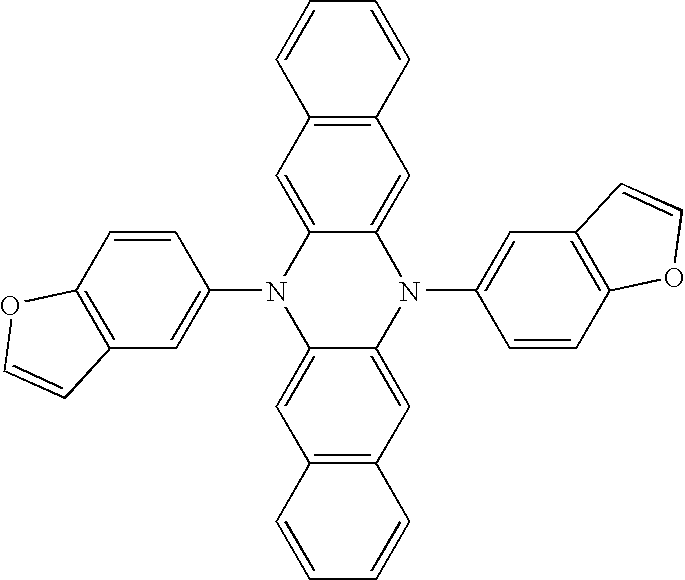
(XLIV) 
(XLV) 
(XLVI) 
(XLVII) 
(XLVIII) 
(XLIX) 
(L) 
(LI) 
(LII) 
(LIII) 
(LIV) 
(LV) 
(LVI) 
(LVII) 
(LVIII) 
(LIX) 
(LX) 
(LXI) 
(LXII) 
(LXIII) 
(LXIV) 
(LXV) 
(LXVI) 
(LXVII) 
(LXVIII) 
(LXIX) 
(LXX) 
(LXXI) 
(LXXII) 
(LXXIII) 
(LXXIV) 
(LXXV) 
(LXXVI) 
(LXXVII) 
(LXXVIII) 
(LXXIX) 
(LXXX) 
(LXXXI) 
(LXXXII) 
(LXXXIII) 
(LXXXIV) 
(LXXXV) 
(LXXXVI) 
(LXXXVII) 
(LXXXVIII) 
(LXXXIX) 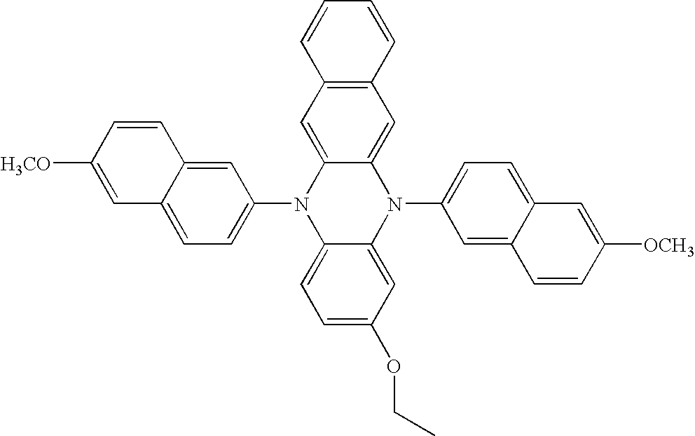
(XC) 
(XCI) 
(XCII) - The following device examples are presented for a further understanding of the present invention. For purposes of brevity, the materials and layers formed therefrom will be abbreviated as given below.
ITO: indium-tin-oxide; used in forming the transparent anode on glass substrates CFx: polymerized fluorocarbon layer; used in forming a hole-injecting layer on top of ITO NPB: N,N′-di(naphthalene-1-yl)-N,N′-diphenyl-benzidine; used in forming the hole-transporting layer in the organic EL unit, and also used as the host in forming the p-type doped organic layer in the connecting unit Alq: tris(8-hydroxyquinoline)aluminum(III); used in forming both the electron-transporting layer in the organic EL unit, and also used as host in forming the n-type doped organic layer in the connecting unit F4- 2,3,5,6-tetrafluoro-7,7′,8,8′-tetracyanoquinodimethane; used as TCNQ: p-type dopant in forming the p-type doped organic layer in the connecting unit Li: Lithium; used as n-type dopant in forming the n-type doped organic layer in the connecting unit Mg:Ag: magnesium:silver at a ratio of 10:0.5 by volume; used in forming the cathode. - The electroluminescence characteristics of all the fabricated devices were evaluated using a constant current source and a photometer at room temperature. The fabricated devices are operated at 20 mA/cm 2 and at the room temperature for operational stability test.
- The preparation of a conventional non-cascaded OLED is as follows. A ˜1.1 mm thick glass substrate coated with a transparent ITO conductive layer was cleaned and dried using a commercial glass scrubber tool. The thickness of ITO is about 42 nm and the sheet resistance of the ITO is about 68 Ω/square. The ITO surface was subsequently treated with oxidative plasma to condition the surface as an anode. A layer of CFx, 1 nm thick, was deposited on the clean ITO surface as the HIL by decomposing CHF 3 gas in RF plasma treatment chamber. The substrate was then transferred into a vacuum deposition chamber for deposition of all other layers on top of the substrate. The following layers were deposited in the following sequence by sublimation from a heated boat under a vacuum of approximately 10−6 Torr:
- (1) a HTL, 75 nm thick, consisting of NPB;
- (2) an ETL (also serving as the emissive layer), 60 nm thick, consisting of Alq;
- (3) a cathode, approximately 210 nm thick, consisting of Mg:Ag.
- After the deposition of these layers, the device was transferred from the deposition chamber into a dry box for encapsulation. The completed device structure is denoted as ITO/CFx/NPB(75)/Alq(60)/Mg:Ag.
- This device requires a driving voltage of 7.3 V to pass 20 mA/cm 2. Its luminance is 495 cd/m2 and its luminance efficiency is about 2.5 cd/A. The luminance decay vs. operational time is shown in both FIGS. 3 and 5, and the voltage evolution vs. operational time is shown in both FIGS. 4 and 6. After 300 hours' operation, the luminance is dropped by about 20%, but the driving voltage is basically unchanged.
- The preparation of a cascaded OLED is as follows. A 1.1 mm thick glass substrate coated with a transparent ITO conductive layer was cleaned and dried using a commercial glass scrubber tool. The thickness of ITO is about 42 nm and the sheet resistance of the ITO is about 68 Ω/square. The ITO surface was subsequently treated with oxidative plasma to condition the surface as an anode. A layer of CFx, 1 nm thick, was deposited on the clean ITO surface as the HIL by decomposing CHF 3 gas in RF plasma treatment chamber. The substrate was then transferred into a vacuum deposition chamber for deposition of all other layers on top of the substrate. The following layers were deposited in the following sequence by sublimation from a heated boat under a vacuum of approximately 10−6 Torr:
- (1) a HTL, 90 nm thick, consisting of NPB;
- (2) an ETL (also serving as the emissive layer), 30 nm thick, consisting of Alq;
- [NPB(90 nm)/Alq(30 nm), denoted as EL1, consists of the 1 st EL unit];
- (3) a n-type doped organic layer, 30 nm thick, consisting of Alq host doped with 1.2 vol. % Li;
- (4) a p-type doped organic layer, 60 nm thick, consisting of NPB host doped with 6 vol. % F 4-TCNQ
- [Li doped Alq(30 nm)/F 4-TCNQ doped NPB(60 nm) consists of the 1st connecting unit];
- (5) a HTL, 30 nm thick, consisting of NPB;
- (6) a LEL, 30 nm thick, consisting of Alq;
- (7) an
ETL 30 nm thick, consisting of Alq host doped with 1.2 vol. % Li; - [NPB(30 nm)/Alq(30 nm)/Alq:Li(30 nm), denoted as EL2, consists of the 2 nd EL unit;
- (8) a cathode, approximately 210 nm thick, consisting of Mg:Ag.
- After the deposition of these layers, the device was transferred from the deposition chamber into a dry box for encapsulation. The completed device structure is denoted as ITO/CFx/EL1/Alq:Li(30 nm)/NPB:F4-TCNQ(60 nm)/EL2/Mg:Ag.
- This cascaded OLED requires a driving voltage of 14.3 V to pass 20 mA/cm 2. Its luminance is 1166 cd/m2 and its luminance efficiency is about 5.8 cd/A, which are twice as high as those of Example 1. The luminance decay vs. operational time is shown in both FIGS. 3 and 5. After 300 hours' operation, the luminance is dropped by about 15%. The voltage evolution vs. operational time is shown in both FIGS. 4 and 6. It is obvious that the driving voltage is operationally unstable. After 300 hours' operation, the driving voltage is increased by 50%.
- A cascaded OLED was fabricated as the same as Example 2 except that NPB was replaced with compound (VI).
- The cascaded device structure is denoted as ITO/CFx/EL1/Alq:Li(30 nm)/(compound VI):F 4-TCNQ(60 nm)/EL2/Mg:Ag.
- This cascaded OLED requires a driving voltage of 13.5 V to pass 20 mA/cm 2. Its luminance is 1611 cd/m2 and its luminance efficiency is about 8.1 cd/A. The efficiency is higher while the voltage is lower when compared to Example 2. The luminance decay vs. operational time is shown in FIG. 3. After 300 hours' operation, the luminance dropped by about 10%. The voltage evolution vs. operational time is shown is FIG. 4. The voltage increased by only 1.3%
- A cascaded OLED was fabricated as the same as Example 2 except that NPB was replaced with compound (VII).
- The cascaded device structure is denoted as ITO/CFx/EL1/Alq:Li(30 nm)/(compound VII):F 4-TCNQ(60 nm)/EL2/Mg:Ag.
- This cascaded OLED requires a driving voltage of 13.2 V to pass 20 m/cm 2. Its luminance is 1619 cd/m2 and its luminance efficiency is about 8.1 cd/A. The efficiency is higher and the voltage is lower when compared to Example 2. The luminance decay vs. operational time is shown in FIG. 3. After 300 hours' operation, the luminance dropped by about 12%. The voltage evolution vs. operational time is shown in FIG. 4. There was no voltage increase.
- A cascaded OLED was fabricated as the same as Example 2 except that NPB was replaced with compound (X).
- The cascaded device structure is denoted as ITO/CFx/EL1/Alq:Li(30 nm)/(compound X):F 4-TCNQ(60 nm)/EL2/Mg:Ag.
- This cascaded OLED requires a driving voltage of 15.3 V to pass 20 mA/cm 2. Its luminance is 1580 cd/m2 and its luminance efficiency is about 7.9 cd/A. The efficiency is higher and the voltage is slightly higher when compared to Example 2. The luminance decay vs. operational time is shown in FIG. 3. After 300 hours' operation, the luminance dropped by about 15%. The voltage evolution vs. operational time is shown in FIG. 4. There was no voltage increase.
- A cascaded OLED was fabricated as the same as Example 2 except that NPB was replaced with compound (XIII).
- The cascaded device structure is denoted as ITO/CFx/EL1/Alq:Li(30 nm)/(compound XIII):F 4-TCNQ(60 nm)/EL2/Mg:Ag.
- This cascaded OLED requires a driving voltage of 12.5 V to pass 20 mA/cm 2. Its luminance is 1466 cd/m2 and its luminance efficiency is about 7.3 cd/A. The efficiency is higher and the voltage is slightly less when compared to Example 2. The luminance decay vs. operational time is shown in FIG. 5. After 300 hours' operation, the luminance dropped by about 14%. The voltage evolution vs. operational time is shown in FIG. 6. There is a voltage increase of about 23%.
- A cascaded OLED was fabricated as the same as Example 2 except that NPB was replaced with compound (XIV).
- The cascaded device structure is denoted as ITO/CFx/EL1/Alq:Li(30 nm)/(compound XIV):F 4-TCNQ(60 nm)/EL2/Mg:Ag.
- This cascaded OLED requires a driving voltage of 15.8 V to pass 20 mA/cm 2. Its luminance is 1598 cd/m2 and its luminance efficiency is about 8.0 cd/A. The efficiency is higher and the voltage is a bit higher when compared to Example 2. The luminance decay vs. operational time is shown in FIG. 5. After 300 hours' operation, the luminance dropped by about 20%. The voltage evolution vs. operational time is shown in FIG. 6. There is a voltage increase of about 2.8%.
- A cascaded OLED was fabricated as the same as Example 2 except that NPB was replaced with compound (XV).
- The cascaded device structure is denoted as ITO/CFx/EL1/Alq:Li(30 nm)/(compound XV):F 4-TCNQ(60 nm)/EL2/Mg:Ag.
- This cascaded OLED requires a driving voltage of 12.7 V to pass 20 mA/cm 2. Its luminance is 1427 cd/m2 and its luminance efficiency is about 7.1 cd/A. The efficiency is higher and the voltage is slightly when compared to Example 2. The luminance decay vs. operational time is shown in FIG. 5. After 300 hours' operation, the luminance dropped by about 14%. The voltage evolution vs. operational time is shown in FIG. 6. There is a voltage increase of about 6.9%.
- A cascaded OLED was fabricated as the same as Example 2 except that NPB was replaced with compound (XIV) and a 4-nm-thick Sb 2O5 layer was disposed between the Li doped Alq layer and the F4-TCNQ doped compound (XIV) layer in the connecting unit.
- The cascaded device structure is denoted as ITO/CFx/EL1/Alq:Li(30 nm)/Sb 2O5(4 nm)/(compound XIV):F4-TCNQ(60 nm)/EL2/Mg:Ag.
- This cascaded OLED requires a driving voltage of 15.5 V to pass 20 mA/cm 2. Its luminance is 1589 cd/m2 and its luminance efficiency is about 8.0 cd/A. When compared to Example 7, the efficiency is about the same and the voltage is slightly lower. The luminance decay vs. operational time is shown in FIG. 7. After 300 hours' operation, the luminance dropped by about 12%. The voltage evolution vs. operational time is shown in FIG. 8. There is no voltage increase during the 300 hours operation of the device.
- The above examples demonstrate that a significant increase in luminance efficiency can be achieved by using a cascaded OLED structure containing the new p-type host materials of the present invention compared to the cascaded OLED using NPB as p-type host. Additionally, the voltage is considerably more stable for the new p-type hosts versus that of NPB. As is shown by Example 9, the voltage can be stabilized even further if we insert an interfacial layer.
- The invention has been described in detail with particular reference to certain preferred embodiments thereof, but it will be understood that variations and modifications can be effected within the spirit and scope of the invention.
- 100 cascaded OLED
- 110 anode
- 120 EL unit
- 120.1 1st EL unit
- 120.2 2nd EL unit
- 120. 3rd EL unit
- 120.(N−1) (N−1)th EL unit
- 120.N Nth EL unit
- 130 connecting unit
- 130.1 1st connecting unit
- 130.2 2nd connecting unit
- 130.(N−1) (N−1)th connecting unit
- 131 n-type doped organic layer
- 132 interfacial layer
- 133 p-type doped organic layer
- 140 cathode
- 150 voltage/current source
- 160 electrical conductors
Claims (15)


Priority Applications (6)
| Application Number | Priority Date | Filing Date | Title |
|---|---|---|---|
| US10/391,176 US6869699B2 (en) | 2003-03-18 | 2003-03-18 | P-type materials and mixtures for electronic devices |
| TW093102309A TWI348490B (en) | 2003-03-18 | 2004-02-02 | A p-type mixture for use in an electronic device |
| EP04075751A EP1463130A2 (en) | 2003-03-18 | 2004-03-09 | P-type materials and mixtures for electronic devices |
| KR1020040017885A KR20040082319A (en) | 2003-03-18 | 2004-03-17 | P-type materials and mixtures for electronic devices |
| JP2004076498A JP4813769B2 (en) | 2003-03-18 | 2004-03-17 | P-type material mixture for electronic devices |
| CNB2004100287934A CN100483773C (en) | 2003-03-18 | 2004-03-18 | P type material and mikture used for electronic device |
Applications Claiming Priority (1)
| Application Number | Priority Date | Filing Date | Title |
|---|---|---|---|
| US10/391,176 US6869699B2 (en) | 2003-03-18 | 2003-03-18 | P-type materials and mixtures for electronic devices |
Publications (2)
| Publication Number | Publication Date |
|---|---|
| US20040183066A1 true US20040183066A1 (en) | 2004-09-23 |
| US6869699B2 US6869699B2 (en) | 2005-03-22 |
Family
ID=32824854
Family Applications (1)
| Application Number | Title | Priority Date | Filing Date |
|---|---|---|---|
| US10/391,176 Expired - Lifetime US6869699B2 (en) | 2003-03-18 | 2003-03-18 | P-type materials and mixtures for electronic devices |
Country Status (6)
| Country | Link |
|---|---|
| US (1) | US6869699B2 (en) |
| EP (1) | EP1463130A2 (en) |
| JP (1) | JP4813769B2 (en) |
| KR (1) | KR20040082319A (en) |
| CN (1) | CN100483773C (en) |
| TW (1) | TWI348490B (en) |
Cited By (14)
| Publication number | Priority date | Publication date | Assignee | Title |
|---|---|---|---|---|
| US20040185297A1 (en) * | 2003-03-18 | 2004-09-23 | Eastman Kodak Company | Cascaded organic electroluminescent devices |
| US20050173700A1 (en) * | 2004-02-06 | 2005-08-11 | Eastman Kodak Company | Full-color organic display having improved blue emission |
| US20050218418A1 (en) * | 2003-06-26 | 2005-10-06 | Eastman Kodak Company | Stacked OLED display having improved efficiency |
| US20050260451A1 (en) * | 2004-05-24 | 2005-11-24 | Sony Corporation | Organic electroluminescence element and display device constructed therefrom |
| US20060131562A1 (en) * | 2004-12-16 | 2006-06-22 | Au Optronics Corporation | Organic light-emitting device with improved layer structure |
| EP1900008A1 (en) * | 2005-06-29 | 2008-03-19 | Eastman Kodak Company | White light tandem oled display with filters |
| EP1908135A1 (en) * | 2005-06-29 | 2008-04-09 | Eastman Kodak Company | Broadband light tandem oled display |
| US20090091246A1 (en) * | 2005-05-11 | 2009-04-09 | Hiroya Tsuji | Organic electroluminescence element |
| DE102009046859A1 (en) * | 2009-11-19 | 2011-06-30 | Sensient Imaging Technologies GmbH, 06766 | Organic solar cell, useful e.g. in portable electronic applications, comprises a photoactive layer, two electrodes on both sides of the photoactive layer, an electron conducting layer, and a hole transport layer |
| US20120146009A1 (en) * | 2009-10-28 | 2012-06-14 | Sharp Kabushiki Kaisha | Novel compound, field-effective transistor, solar cell, method for producing said compound, field-effective transistor, and solar cell, composition for organic semiconductor layer, and composition for p-type semiconductor layer |
| CN103985818A (en) * | 2014-04-01 | 2014-08-13 | 上海道亦化工科技有限公司 | Organic electroluminescent device |
| CN104752624A (en) * | 2013-12-31 | 2015-07-01 | 乐金显示有限公司 | White organic light emitting device |
| US20150333270A1 (en) * | 2009-09-07 | 2015-11-19 | Semiconductor Energy Laboratory Co., Ltd. | Light-Emitting Element, Light-Emitting Device, Lighting Device, and Electronic Device |
| US9991461B2 (en) * | 2015-03-16 | 2018-06-05 | Pioneer Corporation | Light emitting device |
Families Citing this family (23)
| Publication number | Priority date | Publication date | Assignee | Title |
|---|---|---|---|---|
| US8796670B2 (en) | 2003-12-26 | 2014-08-05 | Semiconductor Energy Laboratory Co., Ltd. | Light-emitting element |
| WO2006081780A1 (en) * | 2005-02-04 | 2006-08-10 | Novaled Ag | Dopants for organic semiconductors |
| US7494722B2 (en) | 2005-02-23 | 2009-02-24 | Eastman Kodak Company | Tandem OLED having an organic intermediate connector |
| DE102005039608A1 (en) * | 2005-08-19 | 2007-03-01 | Ormecon Gmbh | Composition with intrinsically conductive polymer |
| US7563860B2 (en) * | 2006-04-06 | 2009-07-21 | Xerox Corporation | Semiconductors and electronic devices generated therefrom |
| US7517477B2 (en) * | 2006-04-06 | 2009-04-14 | Xerox Corporation | Polydiazaacenes and electronic devices generated therefrom |
| US7517476B2 (en) * | 2006-04-06 | 2009-04-14 | Xerox Corporation | Polydiazaacenes |
| TW200812129A (en) * | 2006-08-18 | 2008-03-01 | Chunghwa Picture Tubes Ltd | Organic light emitting structure |
| KR101513311B1 (en) | 2006-09-29 | 2015-04-22 | 유니버시티 오브 플로리다 리서치 파운데이션, 인크. | Method and apparatus for infrared detection and display |
| DE102007023876A1 (en) * | 2007-03-02 | 2008-09-04 | Osram Opto Semiconductors Gmbh | Electric organic component comprises substrate, former electrode, which has anode, former electrically semiconducting layer on former electrode, organic functional layer on former electrically semiconducting layer |
| US8608573B2 (en) | 2008-03-29 | 2013-12-17 | Hemanth Gundurao Kanekal | Electronic trading card and game system |
| CA2800549A1 (en) | 2010-05-24 | 2011-12-01 | University Of Florida Research Foundation, Inc. | Method and apparatus for providing a charge blocking layer on an infrared up-conversion device |
| WO2012067139A1 (en) * | 2010-11-16 | 2012-05-24 | シャープ株式会社 | Compound, field-effect transistor and process for production thereof, solar cell and process for production thereof, organic light-emitting element and process for production thereof, and composition |
| RU2013139230A (en) | 2011-02-28 | 2015-04-10 | Юниверсити Оф Флорида Рисеч Фаундэйшн, Инк. | PHOTODETECTOR AND CONVERTER WITH INCREASED FREQUENCY AND AMPLIFICATION (EP) |
| EP2727154B1 (en) | 2011-06-30 | 2019-09-18 | University of Florida Research Foundation, Inc. | A method and apparatus for detecting infrared radiation with gain |
| KR102268695B1 (en) | 2012-03-15 | 2021-06-23 | 메르크 파텐트 게엠베하 | Electronic devices |
| JP5594750B2 (en) | 2012-05-17 | 2014-09-24 | 国立大学法人九州大学 | COMPOUND, LIGHT EMITTING MATERIAL AND ORGANIC LIGHT EMITTING DEVICE |
| US20150239880A1 (en) | 2012-08-30 | 2015-08-27 | Kyushu University National University Corp. | Light emitting material, compound, and organic light emitting device using the same |
| JP2014082421A (en) | 2012-10-18 | 2014-05-08 | Samsung Display Co Ltd | Organic el material including amine derivative including 5,10-diaryl-5,10-dihydrophenazine moiety, and organic el element using the same |
| EP3308113A4 (en) | 2015-06-11 | 2019-03-20 | University of Florida Research Foundation, Incorporated | Monodisperse, ir-absorbing nanoparticles and related methods and devices |
| CN112079786B (en) * | 2019-06-14 | 2024-05-21 | 北京鼎材科技有限公司 | Compound, organic electronic light-emitting device containing compound and application of compound |
| CN111072578A (en) | 2019-11-25 | 2020-04-28 | 武汉华星光电半导体显示技术有限公司 | P-type dopant and organic light emitting diode |
| CN114914372A (en) * | 2021-02-06 | 2022-08-16 | 北京夏禾科技有限公司 | Organic electroluminescent device |
Citations (11)
| Publication number | Priority date | Publication date | Assignee | Title |
|---|---|---|---|---|
| US3173050A (en) * | 1962-09-19 | 1965-03-09 | Dow Chemical Co | Electroluminescent cell |
| US3172862A (en) * | 1960-09-29 | 1965-03-09 | Dow Chemical Co | Organic electroluminescent phosphors |
| US3710167A (en) * | 1970-07-02 | 1973-01-09 | Rca Corp | Organic electroluminescent cells having a tunnel injection cathode |
| US4356429A (en) * | 1980-07-17 | 1982-10-26 | Eastman Kodak Company | Organic electroluminescent cell |
| US4505841A (en) * | 1982-11-17 | 1985-03-19 | Chevron Research Company | Fused 6,6,6-membered heterocyclic electroactive polymers |
| US4769292A (en) * | 1987-03-02 | 1988-09-06 | Eastman Kodak Company | Electroluminescent device with modified thin film luminescent zone |
| US5703436A (en) * | 1994-12-13 | 1997-12-30 | The Trustees Of Princeton University | Transparent contacts for organic devices |
| US6274980B1 (en) * | 1998-11-16 | 2001-08-14 | The Trustees Of Princeton University | Single-color stacked organic light emitting device |
| US6337492B1 (en) * | 1997-07-11 | 2002-01-08 | Emagin Corporation | Serially-connected organic light emitting diode stack having conductors sandwiching each light emitting layer |
| US6486601B1 (en) * | 1998-06-26 | 2002-11-26 | Idemitsu Kosan Co., Ltd. | Organic luminescence device with reduced leakage current |
| US20040004433A1 (en) * | 2002-06-26 | 2004-01-08 | 3M Innovative Properties Company | Buffer layers for organic electroluminescent devices and methods of manufacture and use |
Family Cites Families (6)
| Publication number | Priority date | Publication date | Assignee | Title |
|---|---|---|---|---|
| EP0136833A3 (en) * | 1983-09-02 | 1986-02-19 | Bolwell Developments Pty. Ltd. | Simulator device |
| JP3150750B2 (en) * | 1992-03-13 | 2001-03-26 | 日本写真印刷株式会社 | Organic rectifier |
| JP3580078B2 (en) * | 1997-04-07 | 2004-10-20 | 東洋インキ製造株式会社 | Organic electroluminescent device material and organic electroluminescent device using the same |
| JP3503403B2 (en) * | 1997-03-17 | 2004-03-08 | 東洋インキ製造株式会社 | Light emitting material for organic electroluminescent device and organic electroluminescent device using the same |
| JP2000021574A (en) | 1998-06-29 | 2000-01-21 | Canon Inc | Light emitting element |
| JP2000260565A (en) * | 1999-03-04 | 2000-09-22 | Futaba Corp | Organic el element |
-
2003
- 2003-03-18 US US10/391,176 patent/US6869699B2/en not_active Expired - Lifetime
-
2004
- 2004-02-02 TW TW093102309A patent/TWI348490B/en not_active IP Right Cessation
- 2004-03-09 EP EP04075751A patent/EP1463130A2/en not_active Withdrawn
- 2004-03-17 KR KR1020040017885A patent/KR20040082319A/en not_active Application Discontinuation
- 2004-03-17 JP JP2004076498A patent/JP4813769B2/en not_active Expired - Lifetime
- 2004-03-18 CN CNB2004100287934A patent/CN100483773C/en not_active Expired - Lifetime
Patent Citations (11)
| Publication number | Priority date | Publication date | Assignee | Title |
|---|---|---|---|---|
| US3172862A (en) * | 1960-09-29 | 1965-03-09 | Dow Chemical Co | Organic electroluminescent phosphors |
| US3173050A (en) * | 1962-09-19 | 1965-03-09 | Dow Chemical Co | Electroluminescent cell |
| US3710167A (en) * | 1970-07-02 | 1973-01-09 | Rca Corp | Organic electroluminescent cells having a tunnel injection cathode |
| US4356429A (en) * | 1980-07-17 | 1982-10-26 | Eastman Kodak Company | Organic electroluminescent cell |
| US4505841A (en) * | 1982-11-17 | 1985-03-19 | Chevron Research Company | Fused 6,6,6-membered heterocyclic electroactive polymers |
| US4769292A (en) * | 1987-03-02 | 1988-09-06 | Eastman Kodak Company | Electroluminescent device with modified thin film luminescent zone |
| US5703436A (en) * | 1994-12-13 | 1997-12-30 | The Trustees Of Princeton University | Transparent contacts for organic devices |
| US6337492B1 (en) * | 1997-07-11 | 2002-01-08 | Emagin Corporation | Serially-connected organic light emitting diode stack having conductors sandwiching each light emitting layer |
| US6486601B1 (en) * | 1998-06-26 | 2002-11-26 | Idemitsu Kosan Co., Ltd. | Organic luminescence device with reduced leakage current |
| US6274980B1 (en) * | 1998-11-16 | 2001-08-14 | The Trustees Of Princeton University | Single-color stacked organic light emitting device |
| US20040004433A1 (en) * | 2002-06-26 | 2004-01-08 | 3M Innovative Properties Company | Buffer layers for organic electroluminescent devices and methods of manufacture and use |
Cited By (21)
| Publication number | Priority date | Publication date | Assignee | Title |
|---|---|---|---|---|
| US20040185297A1 (en) * | 2003-03-18 | 2004-09-23 | Eastman Kodak Company | Cascaded organic electroluminescent devices |
| US6991859B2 (en) * | 2003-03-18 | 2006-01-31 | Eastman Kodak Company | Cascaded organic electroluminescent devices |
| US20050218418A1 (en) * | 2003-06-26 | 2005-10-06 | Eastman Kodak Company | Stacked OLED display having improved efficiency |
| US20050173700A1 (en) * | 2004-02-06 | 2005-08-11 | Eastman Kodak Company | Full-color organic display having improved blue emission |
| US7030554B2 (en) * | 2004-02-06 | 2006-04-18 | Eastman Kodak Company | Full-color organic display having improved blue emission |
| US20050260451A1 (en) * | 2004-05-24 | 2005-11-24 | Sony Corporation | Organic electroluminescence element and display device constructed therefrom |
| US7781073B2 (en) * | 2004-05-24 | 2010-08-24 | Sony Corporation | Organic electroluminescence element and display device constructed therefrom |
| US20060131562A1 (en) * | 2004-12-16 | 2006-06-22 | Au Optronics Corporation | Organic light-emitting device with improved layer structure |
| US7351999B2 (en) * | 2004-12-16 | 2008-04-01 | Au Optronics Corporation | Organic light-emitting device with improved layer structure |
| US20090091246A1 (en) * | 2005-05-11 | 2009-04-09 | Hiroya Tsuji | Organic electroluminescence element |
| US8314545B2 (en) * | 2005-05-11 | 2012-11-20 | Panasonic Corporation | Organic electroluminescence element |
| EP1908135A1 (en) * | 2005-06-29 | 2008-04-09 | Eastman Kodak Company | Broadband light tandem oled display |
| EP1900008A1 (en) * | 2005-06-29 | 2008-03-19 | Eastman Kodak Company | White light tandem oled display with filters |
| EP1900008B1 (en) * | 2005-06-29 | 2017-04-12 | Global OLED Technology LLC | White light tandem oled display with filters |
| US20150333270A1 (en) * | 2009-09-07 | 2015-11-19 | Semiconductor Energy Laboratory Co., Ltd. | Light-Emitting Element, Light-Emitting Device, Lighting Device, and Electronic Device |
| US9917259B2 (en) * | 2009-09-07 | 2018-03-13 | Semiconductor Energy Laboratory Co., Ltd. | Light-emitting element, light-emitting device, lighting device, and electronic device |
| US20120146009A1 (en) * | 2009-10-28 | 2012-06-14 | Sharp Kabushiki Kaisha | Novel compound, field-effective transistor, solar cell, method for producing said compound, field-effective transistor, and solar cell, composition for organic semiconductor layer, and composition for p-type semiconductor layer |
| DE102009046859A1 (en) * | 2009-11-19 | 2011-06-30 | Sensient Imaging Technologies GmbH, 06766 | Organic solar cell, useful e.g. in portable electronic applications, comprises a photoactive layer, two electrodes on both sides of the photoactive layer, an electron conducting layer, and a hole transport layer |
| CN104752624A (en) * | 2013-12-31 | 2015-07-01 | 乐金显示有限公司 | White organic light emitting device |
| CN103985818A (en) * | 2014-04-01 | 2014-08-13 | 上海道亦化工科技有限公司 | Organic electroluminescent device |
| US9991461B2 (en) * | 2015-03-16 | 2018-06-05 | Pioneer Corporation | Light emitting device |
Also Published As
| Publication number | Publication date |
|---|---|
| CN1532959A (en) | 2004-09-29 |
| JP4813769B2 (en) | 2011-11-09 |
| JP2004281408A (en) | 2004-10-07 |
| US6869699B2 (en) | 2005-03-22 |
| CN100483773C (en) | 2009-04-29 |
| EP1463130A2 (en) | 2004-09-29 |
| TWI348490B (en) | 2011-09-11 |
| KR20040082319A (en) | 2004-09-24 |
| TW200500441A (en) | 2005-01-01 |
Similar Documents
| Publication | Publication Date | Title |
|---|---|---|
| US6869699B2 (en) | P-type materials and mixtures for electronic devices | |
| US6991859B2 (en) | Cascaded organic electroluminescent devices | |
| US6717358B1 (en) | Cascaded organic electroluminescent devices with improved voltage stability | |
| US6881502B2 (en) | Blue organic electroluminescent devices having a non-hole-blocking layer | |
| US7494722B2 (en) | Tandem OLED having an organic intermediate connector | |
| US8057916B2 (en) | OLED device with improved performance | |
| US7126267B2 (en) | Tandem OLED having stable intermediate connectors | |
| US8237157B2 (en) | Fluorocarbon electrode modification layer | |
| US6936961B2 (en) | Cascaded organic electroluminescent device having connecting units with N-type and P-type organic layers | |
| US6872472B2 (en) | Providing an organic electroluminescent device having stacked electroluminescent units | |
| US7211948B2 (en) | Using a crystallization-inhibitor in organic electroluminescent devices | |
| US6875320B2 (en) | Highly transparent top electrode for OLED device | |
| EP1668717B1 (en) | Metal sub-layer within a hole-transporting region | |
| US20060240277A1 (en) | Tandem OLED device | |
| US6919140B2 (en) | Organic electroluminescent devices with high luminance |
Legal Events
| Date | Code | Title | Description |
|---|---|---|---|
| AS | Assignment |
Owner name: EASTMAN KODAK COMPANY, NEW YORK Free format text: ASSIGNMENT OF ASSIGNORS INTEREST;ASSIGNORS:KLUBEK, KEVIN P.;LIAO, LIANG-SHENG;VARGAS, J. R.;AND OTHERS;REEL/FRAME:013889/0718;SIGNING DATES FROM 20030313 TO 20030317 |
|
| FEPP | Fee payment procedure |
Free format text: PAYOR NUMBER ASSIGNED (ORIGINAL EVENT CODE: ASPN); ENTITY STATUS OF PATENT OWNER: LARGE ENTITY |
|
| STCF | Information on status: patent grant |
Free format text: PATENTED CASE |
|
| FPAY | Fee payment |
Year of fee payment: 4 |
|
| FEPP | Fee payment procedure |
Free format text: PAYER NUMBER DE-ASSIGNED (ORIGINAL EVENT CODE: RMPN); ENTITY STATUS OF PATENT OWNER: LARGE ENTITY Free format text: PAYOR NUMBER ASSIGNED (ORIGINAL EVENT CODE: ASPN); ENTITY STATUS OF PATENT OWNER: LARGE ENTITY |
|
| AS | Assignment |
Owner name: GLOBAL OLED TECHNOLOGY LLC,DELAWARE Free format text: ASSIGNMENT OF ASSIGNORS INTEREST;ASSIGNOR:EASTMAN KODAK COMPANY;REEL/FRAME:023998/0368 Effective date: 20100122 Owner name: GLOBAL OLED TECHNOLOGY LLC, DELAWARE Free format text: ASSIGNMENT OF ASSIGNORS INTEREST;ASSIGNOR:EASTMAN KODAK COMPANY;REEL/FRAME:023998/0368 Effective date: 20100122 |
|
| FPAY | Fee payment |
Year of fee payment: 8 |
|
| FPAY | Fee payment |
Year of fee payment: 12 |