US20040106064A1 - Silicon-containing polymer, negative type resist composition comprising the same, and patterning method for semiconductor device using the same - Google Patents
Silicon-containing polymer, negative type resist composition comprising the same, and patterning method for semiconductor device using the same Download PDFInfo
- Publication number
- US20040106064A1 US20040106064A1 US10/702,778 US70277803A US2004106064A1 US 20040106064 A1 US20040106064 A1 US 20040106064A1 US 70277803 A US70277803 A US 70277803A US 2004106064 A1 US2004106064 A1 US 2004106064A1
- Authority
- US
- United States
- Prior art keywords
- negative type
- resist composition
- type resist
- group
- base polymer
- Prior art date
- Legal status (The legal status is an assumption and is not a legal conclusion. Google has not performed a legal analysis and makes no representation as to the accuracy of the status listed.)
- Granted
Links
- 0 [1*]C(C)(C)C(=O)OCC Chemical compound [1*]C(C)(C)C(=O)OCC 0.000 description 21
- PGHMAUCFEMMROY-UHFFFAOYSA-N C.C.C.C.C.C.C.C.C=C(C)C(=O)OCC1CO1.C=C(C)C(=O)OCCC[Si](O[Si](C)(C)C)(O[Si](C)(C)C)O[Si](C)(C)C.C=C(C)C(=O)OCCO.CC(C)(C(=O)OCCC[Si](O[Si](C)(C)C)(O[Si](C)(C)C)O[Si](C)(C)C)C(C)(C(=O)OCCO)C(C)(C)C(=O)OCC1CO1 Chemical compound C.C.C.C.C.C.C.C.C=C(C)C(=O)OCC1CO1.C=C(C)C(=O)OCCC[Si](O[Si](C)(C)C)(O[Si](C)(C)C)O[Si](C)(C)C.C=C(C)C(=O)OCCO.CC(C)(C(=O)OCCC[Si](O[Si](C)(C)C)(O[Si](C)(C)C)O[Si](C)(C)C)C(C)(C(=O)OCCO)C(C)(C)C(=O)OCC1CO1 PGHMAUCFEMMROY-UHFFFAOYSA-N 0.000 description 1
- LYUBGQNHPLVLIN-UHFFFAOYSA-N C.C.C.C.C.C.C.C.C=C(C)C(=O)OCC1CO1.C=C(C)C(=O)OCCC[Si](O[Si](C)(C)C)(O[Si](C)(C)C)O[Si](C)(C)C.CC(C)(C(=O)OCCC[Si](O[Si](C)(C)C)(O[Si](C)(C)C)O[Si](C)(C)C)C1C(=O)OC(=O)C1C(C)(C)C(=O)OCC1CO1.O=C1C=CC(=O)O1 Chemical compound C.C.C.C.C.C.C.C.C=C(C)C(=O)OCC1CO1.C=C(C)C(=O)OCCC[Si](O[Si](C)(C)C)(O[Si](C)(C)C)O[Si](C)(C)C.CC(C)(C(=O)OCCC[Si](O[Si](C)(C)C)(O[Si](C)(C)C)O[Si](C)(C)C)C1C(=O)OC(=O)C1C(C)(C)C(=O)OCC1CO1.O=C1C=CC(=O)O1 LYUBGQNHPLVLIN-UHFFFAOYSA-N 0.000 description 1
- IMRRDRRKISHDJJ-UHFFFAOYSA-N C.C.C.C.C.C.C.C.C=C(C)C(=O)OCCC[Si](O[Si](C)(C)C)(O[Si](C)(C)C)O[Si](C)(C)C.C=C(C)C(=O)OCCO.C=CC1=CC=C(O)C=C1.CC(C1=CC=C(O)C=C1)C(C)(C(=O)OCCO)C(C)(C)C(=O)OCCC[Si](O[Si](C)(C)C)(O[Si](C)(C)C)O[Si](C)(C)C Chemical compound C.C.C.C.C.C.C.C.C=C(C)C(=O)OCCC[Si](O[Si](C)(C)C)(O[Si](C)(C)C)O[Si](C)(C)C.C=C(C)C(=O)OCCO.C=CC1=CC=C(O)C=C1.CC(C1=CC=C(O)C=C1)C(C)(C(=O)OCCO)C(C)(C)C(=O)OCCC[Si](O[Si](C)(C)C)(O[Si](C)(C)C)O[Si](C)(C)C IMRRDRRKISHDJJ-UHFFFAOYSA-N 0.000 description 1
- LLIJIKJACSNBBT-UHFFFAOYSA-N C.C.C.C.C.C.C.C.C=C(C)C(=O)OCCC[Si](O[Si](C)(C)C)(O[Si](C)(C)C)O[Si](C)(C)C.C=C(C)C(=O)OCCO.CC(C)(C(=O)OCCO)C1C(=O)OC(=O)C1C(C)(C)C(=O)OCCC[Si](O[Si](C)(C)C)(O[Si](C)(C)C)O[Si](C)(C)C.O=C1C=CC(=O)O1 Chemical compound C.C.C.C.C.C.C.C.C=C(C)C(=O)OCCC[Si](O[Si](C)(C)C)(O[Si](C)(C)C)O[Si](C)(C)C.C=C(C)C(=O)OCCO.CC(C)(C(=O)OCCO)C1C(=O)OC(=O)C1C(C)(C)C(=O)OCCC[Si](O[Si](C)(C)C)(O[Si](C)(C)C)O[Si](C)(C)C.O=C1C=CC(=O)O1 LLIJIKJACSNBBT-UHFFFAOYSA-N 0.000 description 1
- FMTUXMIGAGKTIP-UHFFFAOYSA-N C.C.C.C.C.C=C(C)C(=O)OCC1CO1.C=C(C)C(=O)OCCC[Si](O[Si](C)(C)C)(O[Si](C)(C)C)O[Si](C)(C)C.CC(C)(C(=O)OCCC[Si](O[Si](C)(C)C)(O[Si](C)(C)C)O[Si](C)(C)C)C(C)(C)C(=O)OCC1CO1 Chemical compound C.C.C.C.C.C=C(C)C(=O)OCC1CO1.C=C(C)C(=O)OCCC[Si](O[Si](C)(C)C)(O[Si](C)(C)C)O[Si](C)(C)C.CC(C)(C(=O)OCCC[Si](O[Si](C)(C)C)(O[Si](C)(C)C)O[Si](C)(C)C)C(C)(C)C(=O)OCC1CO1 FMTUXMIGAGKTIP-UHFFFAOYSA-N 0.000 description 1
- YFOHZJAQBSYHGM-UHFFFAOYSA-N C.C.C.C.C.C=C(C)C(=O)OCCC[Si](O[Si](C)(C)C)(O[Si](C)(C)C)O[Si](C)(C)C.C=C(C)C(=O)OCCO.CC(C)(C(=O)OCCO)C(C)(C)C(=O)OCCC[Si](O[Si](C)(C)C)(O[Si](C)(C)C)O[Si](C)(C)C Chemical compound C.C.C.C.C.C=C(C)C(=O)OCCC[Si](O[Si](C)(C)C)(O[Si](C)(C)C)O[Si](C)(C)C.C=C(C)C(=O)OCCO.CC(C)(C(=O)OCCO)C(C)(C)C(=O)OCCC[Si](O[Si](C)(C)C)(O[Si](C)(C)C)O[Si](C)(C)C YFOHZJAQBSYHGM-UHFFFAOYSA-N 0.000 description 1
Images


Classifications
-
- G—PHYSICS
- G03—PHOTOGRAPHY; CINEMATOGRAPHY; ANALOGOUS TECHNIQUES USING WAVES OTHER THAN OPTICAL WAVES; ELECTROGRAPHY; HOLOGRAPHY
- G03F—PHOTOMECHANICAL PRODUCTION OF TEXTURED OR PATTERNED SURFACES, e.g. FOR PRINTING, FOR PROCESSING OF SEMICONDUCTOR DEVICES; MATERIALS THEREFOR; ORIGINALS THEREFOR; APPARATUS SPECIALLY ADAPTED THEREFOR
- G03F7/00—Photomechanical, e.g. photolithographic, production of textured or patterned surfaces, e.g. printing surfaces; Materials therefor, e.g. comprising photoresists; Apparatus specially adapted therefor
- G03F7/004—Photosensitive materials
- G03F7/075—Silicon-containing compounds
-
- C—CHEMISTRY; METALLURGY
- C08—ORGANIC MACROMOLECULAR COMPOUNDS; THEIR PREPARATION OR CHEMICAL WORKING-UP; COMPOSITIONS BASED THEREON
- C08F—MACROMOLECULAR COMPOUNDS OBTAINED BY REACTIONS ONLY INVOLVING CARBON-TO-CARBON UNSATURATED BONDS
- C08F220/00—Copolymers of compounds having one or more unsaturated aliphatic radicals, each having only one carbon-to-carbon double bond, and only one being terminated by only one carboxyl radical or a salt, anhydride ester, amide, imide or nitrile thereof
- C08F220/02—Monocarboxylic acids having less than ten carbon atoms; Derivatives thereof
- C08F220/10—Esters
- C08F220/26—Esters containing oxygen in addition to the carboxy oxygen
-
- G—PHYSICS
- G03—PHOTOGRAPHY; CINEMATOGRAPHY; ANALOGOUS TECHNIQUES USING WAVES OTHER THAN OPTICAL WAVES; ELECTROGRAPHY; HOLOGRAPHY
- G03F—PHOTOMECHANICAL PRODUCTION OF TEXTURED OR PATTERNED SURFACES, e.g. FOR PRINTING, FOR PROCESSING OF SEMICONDUCTOR DEVICES; MATERIALS THEREFOR; ORIGINALS THEREFOR; APPARATUS SPECIALLY ADAPTED THEREFOR
- G03F7/00—Photomechanical, e.g. photolithographic, production of textured or patterned surfaces, e.g. printing surfaces; Materials therefor, e.g. comprising photoresists; Apparatus specially adapted therefor
- G03F7/004—Photosensitive materials
- G03F7/038—Macromolecular compounds which are rendered insoluble or differentially wettable
- G03F7/0382—Macromolecular compounds which are rendered insoluble or differentially wettable the macromolecular compound being present in a chemically amplified negative photoresist composition
-
- G—PHYSICS
- G03—PHOTOGRAPHY; CINEMATOGRAPHY; ANALOGOUS TECHNIQUES USING WAVES OTHER THAN OPTICAL WAVES; ELECTROGRAPHY; HOLOGRAPHY
- G03F—PHOTOMECHANICAL PRODUCTION OF TEXTURED OR PATTERNED SURFACES, e.g. FOR PRINTING, FOR PROCESSING OF SEMICONDUCTOR DEVICES; MATERIALS THEREFOR; ORIGINALS THEREFOR; APPARATUS SPECIALLY ADAPTED THEREFOR
- G03F7/00—Photomechanical, e.g. photolithographic, production of textured or patterned surfaces, e.g. printing surfaces; Materials therefor, e.g. comprising photoresists; Apparatus specially adapted therefor
- G03F7/004—Photosensitive materials
- G03F7/075—Silicon-containing compounds
- G03F7/0757—Macromolecular compounds containing Si-O, Si-C or Si-N bonds
- G03F7/0758—Macromolecular compounds containing Si-O, Si-C or Si-N bonds with silicon- containing groups in the side chains
-
- G—PHYSICS
- G03—PHOTOGRAPHY; CINEMATOGRAPHY; ANALOGOUS TECHNIQUES USING WAVES OTHER THAN OPTICAL WAVES; ELECTROGRAPHY; HOLOGRAPHY
- G03F—PHOTOMECHANICAL PRODUCTION OF TEXTURED OR PATTERNED SURFACES, e.g. FOR PRINTING, FOR PROCESSING OF SEMICONDUCTOR DEVICES; MATERIALS THEREFOR; ORIGINALS THEREFOR; APPARATUS SPECIALLY ADAPTED THEREFOR
- G03F7/00—Photomechanical, e.g. photolithographic, production of textured or patterned surfaces, e.g. printing surfaces; Materials therefor, e.g. comprising photoresists; Apparatus specially adapted therefor
- G03F7/004—Photosensitive materials
- G03F7/09—Photosensitive materials characterised by structural details, e.g. supports, auxiliary layers
- G03F7/095—Photosensitive materials characterised by structural details, e.g. supports, auxiliary layers having more than one photosensitive layer
-
- C—CHEMISTRY; METALLURGY
- C08—ORGANIC MACROMOLECULAR COMPOUNDS; THEIR PREPARATION OR CHEMICAL WORKING-UP; COMPOSITIONS BASED THEREON
- C08F—MACROMOLECULAR COMPOUNDS OBTAINED BY REACTIONS ONLY INVOLVING CARBON-TO-CARBON UNSATURATED BONDS
- C08F230/00—Copolymers of compounds having one or more unsaturated aliphatic radicals, each having only one carbon-to-carbon double bond, and containing phosphorus, selenium, tellurium or a metal
- C08F230/04—Copolymers of compounds having one or more unsaturated aliphatic radicals, each having only one carbon-to-carbon double bond, and containing phosphorus, selenium, tellurium or a metal containing a metal
- C08F230/08—Copolymers of compounds having one or more unsaturated aliphatic radicals, each having only one carbon-to-carbon double bond, and containing phosphorus, selenium, tellurium or a metal containing a metal containing silicon
- C08F230/085—Copolymers of compounds having one or more unsaturated aliphatic radicals, each having only one carbon-to-carbon double bond, and containing phosphorus, selenium, tellurium or a metal containing a metal containing silicon the monomer being a polymerisable silane, e.g. (meth)acryloyloxy trialkoxy silanes or vinyl trialkoxysilanes
-
- Y—GENERAL TAGGING OF NEW TECHNOLOGICAL DEVELOPMENTS; GENERAL TAGGING OF CROSS-SECTIONAL TECHNOLOGIES SPANNING OVER SEVERAL SECTIONS OF THE IPC; TECHNICAL SUBJECTS COVERED BY FORMER USPC CROSS-REFERENCE ART COLLECTIONS [XRACs] AND DIGESTS
- Y10—TECHNICAL SUBJECTS COVERED BY FORMER USPC
- Y10S—TECHNICAL SUBJECTS COVERED BY FORMER USPC CROSS-REFERENCE ART COLLECTIONS [XRACs] AND DIGESTS
- Y10S430/00—Radiation imagery chemistry: process, composition, or product thereof
- Y10S430/1053—Imaging affecting physical property or radiation sensitive material, or producing nonplanar or printing surface - process, composition, or product: radiation sensitive composition or product or process of making binder containing
- Y10S430/1055—Radiation sensitive composition or product or process of making
- Y10S430/106—Binder containing
- Y10S430/111—Polymer of unsaturated acid or ester
-
- Y—GENERAL TAGGING OF NEW TECHNOLOGICAL DEVELOPMENTS; GENERAL TAGGING OF CROSS-SECTIONAL TECHNOLOGIES SPANNING OVER SEVERAL SECTIONS OF THE IPC; TECHNICAL SUBJECTS COVERED BY FORMER USPC CROSS-REFERENCE ART COLLECTIONS [XRACs] AND DIGESTS
- Y10—TECHNICAL SUBJECTS COVERED BY FORMER USPC
- Y10S—TECHNICAL SUBJECTS COVERED BY FORMER USPC CROSS-REFERENCE ART COLLECTIONS [XRACs] AND DIGESTS
- Y10S430/00—Radiation imagery chemistry: process, composition, or product thereof
- Y10S430/1053—Imaging affecting physical property or radiation sensitive material, or producing nonplanar or printing surface - process, composition, or product: radiation sensitive composition or product or process of making binder containing
- Y10S430/1055—Radiation sensitive composition or product or process of making
- Y10S430/114—Initiator containing
- Y10S430/115—Cationic or anionic
-
- Y—GENERAL TAGGING OF NEW TECHNOLOGICAL DEVELOPMENTS; GENERAL TAGGING OF CROSS-SECTIONAL TECHNOLOGIES SPANNING OVER SEVERAL SECTIONS OF THE IPC; TECHNICAL SUBJECTS COVERED BY FORMER USPC CROSS-REFERENCE ART COLLECTIONS [XRACs] AND DIGESTS
- Y10—TECHNICAL SUBJECTS COVERED BY FORMER USPC
- Y10S—TECHNICAL SUBJECTS COVERED BY FORMER USPC CROSS-REFERENCE ART COLLECTIONS [XRACs] AND DIGESTS
- Y10S430/00—Radiation imagery chemistry: process, composition, or product thereof
- Y10S430/1053—Imaging affecting physical property or radiation sensitive material, or producing nonplanar or printing surface - process, composition, or product: radiation sensitive composition or product or process of making binder containing
- Y10S430/1055—Radiation sensitive composition or product or process of making
- Y10S430/114—Initiator containing
- Y10S430/122—Sulfur compound containing
-
- Y—GENERAL TAGGING OF NEW TECHNOLOGICAL DEVELOPMENTS; GENERAL TAGGING OF CROSS-SECTIONAL TECHNOLOGIES SPANNING OVER SEVERAL SECTIONS OF THE IPC; TECHNICAL SUBJECTS COVERED BY FORMER USPC CROSS-REFERENCE ART COLLECTIONS [XRACs] AND DIGESTS
- Y10—TECHNICAL SUBJECTS COVERED BY FORMER USPC
- Y10S—TECHNICAL SUBJECTS COVERED BY FORMER USPC CROSS-REFERENCE ART COLLECTIONS [XRACs] AND DIGESTS
- Y10S430/00—Radiation imagery chemistry: process, composition, or product thereof
- Y10S430/1053—Imaging affecting physical property or radiation sensitive material, or producing nonplanar or printing surface - process, composition, or product: radiation sensitive composition or product or process of making binder containing
- Y10S430/1055—Radiation sensitive composition or product or process of making
- Y10S430/114—Initiator containing
- Y10S430/126—Halogen compound containing
-
- Y—GENERAL TAGGING OF NEW TECHNOLOGICAL DEVELOPMENTS; GENERAL TAGGING OF CROSS-SECTIONAL TECHNOLOGIES SPANNING OVER SEVERAL SECTIONS OF THE IPC; TECHNICAL SUBJECTS COVERED BY FORMER USPC CROSS-REFERENCE ART COLLECTIONS [XRACs] AND DIGESTS
- Y10—TECHNICAL SUBJECTS COVERED BY FORMER USPC
- Y10S—TECHNICAL SUBJECTS COVERED BY FORMER USPC CROSS-REFERENCE ART COLLECTIONS [XRACs] AND DIGESTS
- Y10S430/00—Radiation imagery chemistry: process, composition, or product thereof
- Y10S430/146—Laser beam
Definitions
- the present invention relates generally to silicon-containing polymers, negative type resist compositions comprising the same, and a patterning method for semiconductor devices using the same. More particularly, the present invention relates to silicon-containing polymers for use in a bi-layer resist (BLR) process, negative type resist compositions comprising the same, and a patterning method for semiconductor devices using the same.
- BLR bi-layer resist
- a single layer resist (SLR) process and a bi-layer resist (BLR) process are widely used.
- BLR process overcomes problems associated with the SLR process.
- the BLR process increases the resistance to dry etching. Therefore, patterns having large aspect ratios can be formed using the BLR process and high resolution power can be provided at short-wavelength regions.
- a BLR process requires a two component chemically amplified resist comprising a silicon-containing polymer having a silicon atom substituted in the backbone of the polymer and a photoacid generator (PAG), which is a positive type chemically amplified resist.
- PAG photoacid generator
- high-sensitivity resist materials suitable for the BLR process developed to be compatible with short-wavelength light sources are mostly positive type chemically amplified resists.
- compositions synthesized from the positive type chemically amplified resists suitable for the BLR process are too hydrophobic.
- adhesion to underlying layer materials is weak, and it is difficult to control the amount of silicon needed to create suitable resist materials.
- the most serious problem with the positive type chemically amplified resists is shrinkage by e-beam.
- SEM scanning electron microscope
- CDs critical dimensions
- a polymer having a high transmittance at short-wavelengths and a high dry etching resistance for the manufacture of negative type resist compositions for forming fine patterns in a highly integrated semiconductor device.
- a negative type resist composition that can be used in conjunction with KrF eximer laser (248 nm), ArF excimer laser (193 nm) and next-generation F 2 excimer laser (157 nm), which also provides high dry etching resistance by including silicon and can be advantageously used in a BLR process to realize high resolution power and large aspect ratios.
- a patterning method for a semiconductor device by which fine patterns having large aspect ratios can be formed in highly integrated semiconductor devices.
- a polymer used for a negative type resist composition represented by the following formula:
- R 1 is a hydrogen atom or methyl group
- R 2 is a C 2 ⁇ C 8 alkyl group having a hydroxy group
- R 3 is a hydrogen atom or methyl group
- X is a C 1 -C 4 alkyl or alkoxy group
- n is an integer from 2 to 4
- q/(p+q) is about 0.1 to about 0.5.
- the weight average molecular weight of the polymer is about 3,000 to about 50,000.
- R 2 is a 2-hydroxyethyl or a 2-hydroxypropyl group and X is a methyl group or a trimethylsilyloxy group.
- the polymer may also include at least one repeating unit selected from the group consisting of acrylate derivatives, methacrylate derivatives, norbornene derivatives, maleic anhydride monomer derivatives and styrene derivatives, and the Si-containing repeating unit is contained in the base polymer in an amount of about 5 to about 40 mol % based on total number of moles of repeating units forming the base polymer.
- R 1 is a hydrogen atom or a methyl group
- R 2 is a hydrogen atom or methyl group
- X is a C 1 -C 4 alkyl or alkoxy group
- n is an integer from 2 to 4
- q/(p+q) is about 0.1 to about 0.5.
- the weight average molecular weight of the polymer is about 3,000 to about 50,000.
- X is a methyl group or a trimethylsilyloxy group.
- the polymer may also include at least one repeating unit selected from the group consisting of acrylate derivatives, methacrylate derivatives, norbornene derivatives, maleic anhydride monomer derivatives and styrene derivatives, and wherein the Si-containing repeating unit is contained in the base polymer in an amount of about 5 to about 40 mol % based on total number of moles of repeating units forming the base polymer.
- a negative type resist composition comprising:
- R 1 is a hydrogen atom or methyl group
- X is a C 1 -C 4 alkyl or alkoxy group
- n is an integer from 2 to 4
- a photoacid generator (PAG) and a crosslinking agent cross linkable in the presence of an acid.
- the base polymer has a weight average molecular weight of about 3,000 to about 50,000.
- a patterning method for a semiconductor device comprising forming a first resist layer on a layer to be etched on a semiconductor substrate, forming a second resist layer by coating a negative type resist composition comprising an alkali soluble base polymer, pre-baking the second resist layer, exposing the second resist layer to light, performing post-exposure baking (PEB) on the exposed second resist layer, forming a second resist layer pattern by developing the exposed second resist layer, forming a first resist layer pattern by etching the first resist layer using the second resist layer pattern as an etching mask, and etching the layer to be etched using the first resist layer pattern as an etching mask.
- PEB post-exposure baking
- R 1 is a hydrogen atom or a methyl group
- R 2 is a hydrogen atom or methyl group
- X is a C 1 -C 4 alkyl or alkoxy group
- n is an integer from 2 to 4
- q/(p+q) is about 0.1 to about 0.5
- a photoacid generator (PAG) and a crosslinking agent formed of a compound having a hydroxy group and cross linkable by reacting with an acid.
- FIGS. 1 through 4 are cross-sectional views of a patterning method for semiconductor devices, according to an exemplary embodiment of the present invention.
- a negative type resist composition according to an exemplary embodiment of the present invention includes an alkali soluble base polymer having a repeating unit formed of a Si-containing monomer unit, a photoacid generator (PAG) and a crosslinking agent cross linkable by reacting with an acid.
- PAG photoacid generator
- the base polymer comprises a first repeating unit represented by Formula 1:
- R 1 is a hydrogen atom or a methyl group
- X is a C 1 -C 4 alkyl or alkoxy group
- n is an integer from 2 to 4.
- the base polymer has a weight average molecular weight of about 3,000 to about 50,000.
- X is a methyl group or a trimethylsilyloxy group.
- the base polymer may further include a second repeating unit having a hydroxy group represented by Formula 2:
- R 2 is a hydrogen atom or a methyl group
- R 3 is a C 2 ⁇ C 8 alkyl group having a hydroxy group.
- R 3 is a 2-hydroxyethyl or a 2-hydroxypropyl group.
- the structure of the base polymer can be represented by Formula 3:
- R 1 is a hydrogen atom or a methyl group
- R 2 is a C 2 ⁇ C 8 alkyl group having a hydroxy group
- R 3 is a hydrogen atom or a methyl group
- X is a C 1 -C 4 alkyl or alkoxy group
- n is an integer from 2 to 4
- q/(p+q) is about 0.1 to about 0.5.
- R 2 is a 2-hydroxyethyl group or a 2-hydroxypropyl group.
- a negative type resist composition can be manufactured using a compound having an epoxy ring as a crosslinking agent.
- aliphatic compounds having multi-epoxy groups can be used as the crosslinking agent having an epoxy ring. These aliphatic compounds cause curing with a hydroxy group in the presence of an acid.
- the crosslinking agent having an epoxy ring is a triglycidyl isocyanurate, a trimethylolpropane triglycidyl ether, or a triphenylolmethane triglycidyl ether.
- the base polymer represented by Formula 3 may further include a third repeating unit selected from the group consisting of acrylate derivatives, methacrylate derivatives, norbornene derivatives, maleic anhydride monomer derivatives, and styrene derivatives.
- the Si-containing repeating unit is contained in the base polymer in an amount of about 5 to about 40 mol % based on total number of moles of repeating units forming the base polymer.
- the second repeating unit may be a repeating unit having an epoxy ring represented by the following Formula 4:
- R 4 is a hydrogen atom or a methyl group.
- the structure of the base polymer can be represented by Formula 5:
- R 1 is a hydrogen atom or a methyl group
- R 2 is a hydrogen atom or a methyl group
- X is a C 1 -C 4 alkyl or alkoxy group
- n is an integer from 2 to 4
- q/(p+q) is about 0.1 to about 0.5.
- a negative type resist composition can be manufactured using a compound having a hydroxy group as a crosslinking agent, according to another embodiment of the present invention.
- the crosslinking agent having a hydroxy group used for causing curing with an expoxy ring in the base polymer may be a polymer having three or more different monomer units.
- the crosslinking agent may be a low molecular weight aliphatic compound having a multi-hydroxy group, and the low-molecule weight aliphatic compound may cause curing with an epoxy group in the presence of an acid.
- the crosslinking agent having a hydroxy group is 1,3,5-tris(2-hydroxyethyl)cyanuric acid, 1,1,1-tris(hydroxymethyl)ethane, triethylene glycol, diethylene glycol, 1,2,6-trihydroxyhexane or trimethylolpropane.
- the base polymer represented by Formula 5 may further include a third repeating unit selected from a group consisting of acrylate derivatives, methacrylate derivatives, norbornene derivatives, maleic anhydride monomer derivatives and styrene derivatives.
- the Si-containing repeating unit is contained in the base polymer in an amount of about 5 to about 40 mol % based on total number of moles of repeating units forming the base polymer.
- the third repeating unit includes a (meth)acrylate derivative or norbornene derivative having a hydroxy group.
- PAG is contained in an amount of about 1.0 to about 15% by weight based on the total weight of the base polymer.
- PAG includes onium compounds exemplified by triarylsulfonium salts, diaryliodonium salts, or mixtures thereof. More preferably, the PAG comprises triphenylsulfonium triflate, diphenyliodonium triflate, di-t-butyldiphenyliodonium triflate, or mixtures thereof.
- a negative type resist composition may further comprise an organic base in an amount of about 0.01 to about 2.0 wt % on the basis of the total weight of the base polymer.
- the organic base comprises organic tertiary amine compounds exemplified by triethylamine, triisobutylamine, trioctylamine, triisodecylamine, triethanolamine, or mixtures thereof.
- FIGS. 1 through 4 are cross-sectional views of a patterning method for a semiconductor device according to the present invention.
- an etching target layer 12 is formed on a substrate 10 , for example, a semiconductor substrate or a transparent, and a BLR structure resist layer comprised of a first resist layer 22 and a second resist layer 24 containing silicon is formed by spin coating.
- the second resist layer 24 is a negative type resist composition according to the embodiments of the present invention discussed above.
- pre-baking is performed to provide the second resist layer 24 having a predetermined thickness.
- the predetermined thickness of the second resist layer 24 is about 100 to about 400 nm.
- a selected portion of the second resist layer 24 is exposed to light through a mask 26 using a KrF, ArF or F 2 eximer laser.
- the second resist layer 24 is defined by an exposure portion 24 a and a non-exposure portion 24 b .
- a post exposure bake (PEB) is performed on the exposed second resist layer 24 .
- cross-linkage occurs at the exposure portion 24 a of the second resist layer 24 with the PAG.
- the exposed second resist layer 24 is developed using an alkali solution, e.g., a tetramethylammonium hydroxide (TMAH) solution, to remove the non-exposure portion 24 b , thereby forming a second resist layer pattern 24 a formed of the exposure portion 24 a , which is a negative type pattern.
- an alkali solution e.g., a tetramethylammonium hydroxide (TMAH) solution
- the first resist layer 22 is etched, e.g., using O 2 plasma, using the second resist layer pattern 24 a as an etching mask to form a first resist layer pattern 22 a .
- the etching target layer 12 is etched using the first resist layer pattern 22 a as an etching mask to form an etching target layer pattern 12 a.
- the reactant was slowly precipitated with excess n-hexane. Thereafter, the precipitate was filtered, and the filtrate was dissolved in an appropriate amount of THF and re-precipitated in n-hexane. Then, the obtained precipitate was dried in a vacuum oven at about 50° C. for about 24 hours, giving a desired product at a yield of about 75%.
- the obtained product had a weight average molecular weight (Mw) of about 13,200 and polydispersity (Mw/Mn) of about 1.9.
- the obtained product had a weight average molecular weight (Mw) of about 12,100 and polydispersity (Mw/Mn) of about 2.0.
- the obtained product had a weight average molecular weight (Mw) of about 9,700 and polydispersity (Mw/Mn) of about 1.9.
- the reactant was slowly precipitated with excess n-hexane. Thereafter, the precipitate was filtered, and the filtrate was dissolved in an appropriate amount of THF and re-precipitated in n-hexane. Then, the obtained precipitate was dried in a vacuum oven at about 50° C. for about 24 hours, giving a desired product at a yield of about 75%.
- the obtained product had a weight average molecular weight (Mw) of about 13,500 and polydispersity (Mw/Mn) of about 2.0.
- the obtained product had a weight average molecular weight (Mw) of about 14,100 and polydispersity (Mw/Mn) of about 2.0.
- the obtained product had a weight average molecular weight (Mw) of about 9,100 and polydispersity (Mw/Mn) of about 1.9.
- HMDS hexamethyldisilazane
- PEB post exposure bake
- TMAH tetramethylammonium hydroxide
- a PEB was performed at a temperature of about 120° C. for about 60 seconds.
- the resultant was developed using a solution of TMAH (2.38 wt %) for about 60 seconds.
- TMAH TMAH (2.38 wt %) for about 60 seconds.
- a 150 nm line-and-space pattern was obtained at an exposure dose of about 10 to about 16 mJ/cm 2 .
- PEB post exposure bake
- the resultant was developed using a solution of TMAH (2.38 wt %) for about 60 seconds.
- TMAH TMAH (2.38 wt %)
- a 150 nm line-and-space pattern was obtained at an exposure dose of about 11 to about 15 mJ/cm 2 .
- PEB post exposure bake
- a silicon nitride layer is formed on a Si wafer to a thickness of about 3000 ⁇ and an i-line resist (such as ip3300 manufactured by Tokyo Ohka Kogyo Co.) was coated thereon to a thickness of about 500 nm, followed by thermally treating the Si wafer having the silicon nitride layer and i-line resist at a temperature of about 220° C., thereby forming a bottom layer.
- an i-line resist such as ip3300 manufactured by Tokyo Ohka Kogyo Co.
- PEB post exposure bake
- the bottom layer was etched by a dry etching process using O 2 plasma (source gases: O 2 /SO 2 ) and the top layer pattern as an etching mask to form a bottom layer pattern. Thereafter, the top layer pattern was removed using a stripper.
- O 2 plasma source gases: O 2 /SO 2
- a silicon nitride layer was etched by a dry etching process using a CF 4 plasma and the bottom layer pattern comprised of i-line resist as an etching mask, thereby forming a silicon nitride layer pattern. Then, the resist layer remaining on the wafer was removed using a stripper.
- the crosslinking agent is not limited to the compounds illustrated in the embodiments.
- triglycidyl isocyanurate trimethylolpropane triglycidyl ether or triphenylolmethane triglycidyl ether can also be used as a crosslinking agent.
- 1,3,5-tris(2-hydroxyethyl)cyanuric acid 1,1,1-tris(hydroxymethyl)ethane, triethylene glycol, diethylene glycol, 1,2,6-trihydroxyhexane, or trimethylolpropane can also be used as a crosslinking agent.
- the PAG is used in an amount of about 1.0 to about 15% by weight based on the weight of the base polymer and examples thereof include triarylsulfonium salts, diaryliodonium salts and mixtures thereof.
- the organic base is contained in an amount of about 0.01 to about 2.0 wt % on the basis of the total weight of the base polymer and comprises a tertiary amine exemplified by triethylamine, triisobutylamine, trioctylamine, triisodecylamine, diethanolamine, triethanolamine, or mixtures thereof.
- the thickness of the negative type resist composition coated on the wafer may vary according to use.
- the thickness of the negative type resist composition is about 0.2 to about 0.7 ⁇ m.
- Soft-baking is generally performed at about 110 to about 140° C. for about 60 to about 90 seconds.
- an exposure dose may vary according to a deep-UV used.
- ArF or F 2 eximer laser energy of about 5 to about 100 mJ/cm 2 is generally used.
- the PEB is generally performed at about 100 to about 130° C. for about 60 to about 90 seconds.
- the development is generally performed using a 2.38 wt % TMAH (0.26N) solution for about 20 to about 60 seconds.
- a polymer comprising a first repeating unit having a Si-containing monomer unit.
- the polymer further comprises a second repeating unit having a hydroxy group copolymerized with the first repeating unit.
- the second repeating unit may be a monomer unit having a hydroxy group or a monomer unit having an epoxy ring.
- the polymer having the above-described structure exhibits high transmittance at short wavelengths and provides high dry etching resistance by including silicon therein. Therefore, the polymer can be used for the manufacture of the negative type resist composition that is advantageously used in forming fine patterns.
- the negative type resist composition according to the present invention includes an alkali soluble base polymer having a repeating unit formed of a Si-containing monomer unit, a PAG and a crosslinking agent. If the base polymer includes a Si-containing monomer unit and a monomer unit having an epoxy ring, the crosslinking agent is formed of a compound having a hydroxy group. Therefore, in the case of using the negative type resist composition according to the embodiments of the present invention in a BLR process, the density of a resist layer is increased by cross-linkage. Therefore, shrinkage caused by e-beam, which is the most serious problem with conventional positive type chemically amplified resists, is prevented. Also, compared with the conventional positive type resist composition, a negative type resist composition according to the present invention has improved adhesion to underlying layers and easily adjustably wettability.
- the negative type resist composition according to the embodiments of the present invention exhibits high transmittance at short wavelengths such as a KrF (248 nm), ArF (193 nm), or F 2 (157 nm) eximer laser, and provides high dry etching resistance by including silicon therein. Therefore, the negative type resist composition can be advantageously used in a BLR process. Also, patterns having large aspect ratios, which are required for highly integrated semiconductor devices, can be formed using the BLR process in conjunction with the negative type resist compositions, according to the embodiments of the present invention.
Landscapes
- Physics & Mathematics (AREA)
- General Physics & Mathematics (AREA)
- Spectroscopy & Molecular Physics (AREA)
- Chemical & Material Sciences (AREA)
- Health & Medical Sciences (AREA)
- Structural Engineering (AREA)
- Engineering & Computer Science (AREA)
- Architecture (AREA)
- Chemical Kinetics & Catalysis (AREA)
- Medicinal Chemistry (AREA)
- Polymers & Plastics (AREA)
- Organic Chemistry (AREA)
- Materials For Photolithography (AREA)
- Exposure And Positioning Against Photoresist Photosensitive Materials (AREA)
Abstract

Description
- 1. Technical Field
- The present invention relates generally to silicon-containing polymers, negative type resist compositions comprising the same, and a patterning method for semiconductor devices using the same. More particularly, the present invention relates to silicon-containing polymers for use in a bi-layer resist (BLR) process, negative type resist compositions comprising the same, and a patterning method for semiconductor devices using the same.
- 2. Discussion of the Related Art
- As semiconductor devices become more highly integrated and complex, the ability to form ultra-fine patterns becomes more important. For instance, in semiconductor devices of 1-Gigabit or greater, a pattern size having a design rule of 0.2 μm or less is needed. Such pattern size is difficult to achieve using conventional lithography processes using lower wavelength devices, e.g., a KrF eximer laser (248 nm), with a conventional resist material. Lithography processes using different exposure light sources, e.g., ArF excimer laser (193 nm) or F 2 excimer laser (157 nm), have been proposed.
- Further, conventional ArF or F 2 resist materials suffer from a variety of drawbacks due to their structural limitation. One problem is the increase in the occurrence of patterns collapsing as the aspect ratio of pattern features increases. Another problem is the weak resistance against a dry etching process. Accordingly, there is an increasing demand for the development of new resist materials and processes.
- In photolithography for the manufacture of highly integrated semiconductor devices, a single layer resist (SLR) process and a bi-layer resist (BLR) process are widely used. Use of the BLR process overcomes problems associated with the SLR process. For example, the BLR process increases the resistance to dry etching. Therefore, patterns having large aspect ratios can be formed using the BLR process and high resolution power can be provided at short-wavelength regions.
- Generally, a BLR process requires a two component chemically amplified resist comprising a silicon-containing polymer having a silicon atom substituted in the backbone of the polymer and a photoacid generator (PAG), which is a positive type chemically amplified resist. Also, high-sensitivity resist materials suitable for the BLR process developed to be compatible with short-wavelength light sources are mostly positive type chemically amplified resists.
- Although positive type chemically amplified resists are preferred in view of their higher resolution, compositions synthesized from the positive type chemically amplified resists suitable for the BLR process are too hydrophobic. Thus, adhesion to underlying layer materials is weak, and it is difficult to control the amount of silicon needed to create suitable resist materials. In particular, the most serious problem with the positive type chemically amplified resists is shrinkage by e-beam. In other words, while observing sizes of resist patterns using a scanning electron microscope (SEM), critical dimensions (CDs) of the patterns may change.
- In pursuit of high-speed, highly-efficient DRAMs, there is a limitation in using positive type resists for forming isolated patterns. In lithography processes for the manufacture of semiconductor devices having a memory capacity of 1-Gigabit or more, use of phase shift masks is needed. In the design of phase shift masks, negative type resists are preferred over positive type resists.
- Therefore, there is a need to develop negative type resists having a high transmittance to short-wavelength exposure light sources, high resolution power, and high dry etching resistance.
- Provided is a polymer having a high transmittance at short-wavelengths and a high dry etching resistance for the manufacture of negative type resist compositions for forming fine patterns in a highly integrated semiconductor device.
- Also provided is a negative type resist composition that can be used in conjunction with KrF eximer laser (248 nm), ArF excimer laser (193 nm) and next-generation F 2 excimer laser (157 nm), which also provides high dry etching resistance by including silicon and can be advantageously used in a BLR process to realize high resolution power and large aspect ratios.
- Further, provided is a patterning method for a semiconductor device, by which fine patterns having large aspect ratios can be formed in highly integrated semiconductor devices.
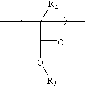
- According to one aspect of the present invention, there is provided a polymer used for a negative type resist composition, represented by the following formula:

- wherein R 1 is a hydrogen atom or methyl group, R2 is a C2˜C8 alkyl group having a hydroxy group, R3 is a hydrogen atom or methyl group, X is a C1-C4 alkyl or alkoxy group, n is an integer from 2 to 4, and q/(p+q) is about 0.1 to about 0.5. And, the weight average molecular weight of the polymer is about 3,000 to about 50,000.
- Preferably, R 2 is a 2-hydroxyethyl or a 2-hydroxypropyl group and X is a methyl group or a trimethylsilyloxy group. Further, the polymer may also include at least one repeating unit selected from the group consisting of acrylate derivatives, methacrylate derivatives, norbornene derivatives, maleic anhydride monomer derivatives and styrene derivatives, and the Si-containing repeating unit is contained in the base polymer in an amount of about 5 to about 40 mol % based on total number of moles of repeating units forming the base polymer.
- In another aspect of the present invention, there is provided a polymer used for a negative type resist composition, represented by the following formula:

- wherein R 1 is a hydrogen atom or a methyl group, R2 is a hydrogen atom or methyl group, X is a C1-C4 alkyl or alkoxy group, n is an integer from 2 to 4, and q/(p+q) is about 0.1 to about 0.5. And, the weight average molecular weight of the polymer is about 3,000 to about 50,000.
- Preferably, X is a methyl group or a trimethylsilyloxy group. Further, the polymer may also include at least one repeating unit selected from the group consisting of acrylate derivatives, methacrylate derivatives, norbornene derivatives, maleic anhydride monomer derivatives and styrene derivatives, and wherein the Si-containing repeating unit is contained in the base polymer in an amount of about 5 to about 40 mol % based on total number of moles of repeating units forming the base polymer.
- According to still another aspect of the present invention, there is provided a negative type resist composition comprising:
- (a) an alkali soluble base polymer having a first repeating unit represented by the following formula:

- wherein R 1 is a hydrogen atom or methyl group, X is a C1-C4 alkyl or alkoxy group, and n is an integer from 2 to 4, a photoacid generator (PAG), and a crosslinking agent cross linkable in the presence of an acid. Further, the base polymer has a weight average molecular weight of about 3,000 to about 50,000.
- According to yet another aspect of the present invention, there is provided a patterning method for a semiconductor device comprising forming a first resist layer on a layer to be etched on a semiconductor substrate, forming a second resist layer by coating a negative type resist composition comprising an alkali soluble base polymer, pre-baking the second resist layer, exposing the second resist layer to light, performing post-exposure baking (PEB) on the exposed second resist layer, forming a second resist layer pattern by developing the exposed second resist layer, forming a first resist layer pattern by etching the first resist layer using the second resist layer pattern as an etching mask, and etching the layer to be etched using the first resist layer pattern as an etching mask.
- Further, the negative type resist composition comprising an alkali soluble base polymer may be represented by the following formula:

- wherein R 1 is a hydrogen atom or a methyl group, R2 is a hydrogen atom or methyl group, X is a C1-C4 alkyl or alkoxy group, n is an integer from 2 to 4, and q/(p+q) is about 0.1 to about 0.5, a photoacid generator (PAG), and a crosslinking agent formed of a compound having a hydroxy group and cross linkable by reacting with an acid.
- Thus, a polymer, a negative type photoresist, and a patterning method for semiconductor devices using the same to solve the problems of the conventional art are disclosed.
- FIGS. 1 through 4 are cross-sectional views of a patterning method for semiconductor devices, according to an exemplary embodiment of the present invention.
- The Embodiments of the present invention will now be described more fully hereinafter with reference to the accompanying drawings where applicable, in which preferred embodiments of the invention are shown. This invention may, however, be embodied in different forms and should not be construed as limited to the embodiments set forth herein. Rather, these embodiments are provided so that this disclosure will be thorough and complete, and will fully convey the scope of the invention to those skilled in the art.
- A negative type resist composition according to an exemplary embodiment of the present invention includes an alkali soluble base polymer having a repeating unit formed of a Si-containing monomer unit, a photoacid generator (PAG) and a crosslinking agent cross linkable by reacting with an acid.
- The base polymer comprises a first repeating unit represented by Formula 1:

- wherein R 1 is a hydrogen atom or a methyl group, X is a C1-C4 alkyl or alkoxy group, and n is an integer from 2 to 4. The base polymer has a weight average molecular weight of about 3,000 to about 50,000.
- Preferably, X is a methyl group or a trimethylsilyloxy group.
- The base polymer may further include a second repeating unit having a hydroxy group represented by Formula 2:

- wherein R 2 is a hydrogen atom or a methyl group, R3 is a C2˜C8 alkyl group having a hydroxy group. Preferably, R3 is a 2-hydroxyethyl or a 2-hydroxypropyl group.
- If the base polymer includes a Si-containing first repeating unit represented by Formula 1 and a second repeating unit having a hydroxy group represented by Formula 2, the structure of the base polymer can be represented by Formula 3:

- wherein R 1 is a hydrogen atom or a methyl group, R2 is a C2˜C8 alkyl group having a hydroxy group, R3 is a hydrogen atom or a methyl group, X is a C1-C4 alkyl or alkoxy group, n is an integer from 2 to 4, and q/(p+q) is about 0.1 to about 0.5. Preferably, R2 is a 2-hydroxyethyl group or a 2-hydroxypropyl group.
- In the case of using the base polymer represented by Formula 3, a negative type resist composition can be manufactured using a compound having an epoxy ring as a crosslinking agent. In the manufacture of the negative type resist composition, aliphatic compounds having multi-epoxy groups can be used as the crosslinking agent having an epoxy ring. These aliphatic compounds cause curing with a hydroxy group in the presence of an acid.
- Preferably, the crosslinking agent having an epoxy ring is a triglycidyl isocyanurate, a trimethylolpropane triglycidyl ether, or a triphenylolmethane triglycidyl ether.
- The base polymer represented by Formula 3 may further include a third repeating unit selected from the group consisting of acrylate derivatives, methacrylate derivatives, norbornene derivatives, maleic anhydride monomer derivatives, and styrene derivatives. Preferably, the Si-containing repeating unit is contained in the base polymer in an amount of about 5 to about 40 mol % based on total number of moles of repeating units forming the base polymer.
- The second repeating unit may be a repeating unit having an epoxy ring represented by the following Formula 4:

- wherein R 4 is a hydrogen atom or a methyl group.
- If the base polymer includes a Si-containing first repeating unit represented by Formula 1 and a second repeating unit having an epoxy ring represented by Formula 4, the structure of the base polymer can be represented by Formula 5:

- wherein R 1 is a hydrogen atom or a methyl group, R2 is a hydrogen atom or a methyl group, X is a C1-C4 alkyl or alkoxy group, n is an integer from 2 to 4, and q/(p+q) is about 0.1 to about 0.5.
- In the case of using the base polymer represented by Formula 5, a negative type resist composition can be manufactured using a compound having a hydroxy group as a crosslinking agent, according to another embodiment of the present invention. In the manufacture of the negative type resist composition, the crosslinking agent having a hydroxy group used for causing curing with an expoxy ring in the base polymer may be a polymer having three or more different monomer units. In addition, the crosslinking agent may be a low molecular weight aliphatic compound having a multi-hydroxy group, and the low-molecule weight aliphatic compound may cause curing with an epoxy group in the presence of an acid.
- Preferably, the crosslinking agent having a hydroxy group is 1,3,5-tris(2-hydroxyethyl)cyanuric acid, 1,1,1-tris(hydroxymethyl)ethane, triethylene glycol, diethylene glycol, 1,2,6-trihydroxyhexane or trimethylolpropane.
- The base polymer represented by Formula 5 may further include a third repeating unit selected from a group consisting of acrylate derivatives, methacrylate derivatives, norbornene derivatives, maleic anhydride monomer derivatives and styrene derivatives. Preferably, the Si-containing repeating unit is contained in the base polymer in an amount of about 5 to about 40 mol % based on total number of moles of repeating units forming the base polymer. Preferably, the third repeating unit includes a (meth)acrylate derivative or norbornene derivative having a hydroxy group.
- In the manufacture of the negative type resist composition according to another exemplary embodiment of the present invention, PAG is contained in an amount of about 1.0 to about 15% by weight based on the total weight of the base polymer. Preferably, PAG includes onium compounds exemplified by triarylsulfonium salts, diaryliodonium salts, or mixtures thereof. More preferably, the PAG comprises triphenylsulfonium triflate, diphenyliodonium triflate, di-t-butyldiphenyliodonium triflate, or mixtures thereof.
- According to another embodiment of the present invention, a negative type resist composition may further comprise an organic base in an amount of about 0.01 to about 2.0 wt % on the basis of the total weight of the base polymer. Preferably, the organic base comprises organic tertiary amine compounds exemplified by triethylamine, triisobutylamine, trioctylamine, triisodecylamine, triethanolamine, or mixtures thereof.
- FIGS. 1 through 4 are cross-sectional views of a patterning method for a semiconductor device according to the present invention.
- First, referring to FIG. 1, an
etching target layer 12 is formed on asubstrate 10, for example, a semiconductor substrate or a transparent, and a BLR structure resist layer comprised of a first resistlayer 22 and a second resistlayer 24 containing silicon is formed by spin coating. The second resistlayer 24 is a negative type resist composition according to the embodiments of the present invention discussed above. After the negative type resist composition is spin coated on the first resistlayer 22, pre-baking is performed to provide the second resistlayer 24 having a predetermined thickness. Preferably, the predetermined thickness of the second resistlayer 24 is about 100 to about 400 nm. - Referring to FIG. 2, a selected portion of the second resist
layer 24 is exposed to light through amask 26 using a KrF, ArF or F2 eximer laser. Thus, the second resistlayer 24 is defined by anexposure portion 24 a and anon-exposure portion 24 b. Then, a post exposure bake (PEB) is performed on the exposed second resistlayer 24. And, cross-linkage occurs at theexposure portion 24 a of the second resistlayer 24 with the PAG. - Referring to FIG. 3, the exposed second resist
layer 24 is developed using an alkali solution, e.g., a tetramethylammonium hydroxide (TMAH) solution, to remove thenon-exposure portion 24 b, thereby forming a second resistlayer pattern 24 a formed of theexposure portion 24 a, which is a negative type pattern. - Referring to FIG. 4, the first resist
layer 22 is etched, e.g., using O2 plasma, using the second resistlayer pattern 24 a as an etching mask to form a first resistlayer pattern 22 a. Subsequently, theetching target layer 12 is etched using the first resistlayer pattern 22 a as an etching mask to form an etchingtarget layer pattern 12 a. - The present invention will now be described in more detail with reference to the following illustrative examples. Further, the following illustrative examples may be altered in various forms and the invention should not be construed as limited thereto.
-

- 4.3 g of 3-[tris(trimethylsilyloxy)silyl]propyl methacrylate (10 mmol) and 3.9 g of 2-hydroxyethyl methacrylate (30 mmol) were dissolved in a round bottom flask containing 35 g of tetrahydrofuran (THF) and 0.33 g of azobisisobutyronitrile (AIBN) (5 mol %) and purged using nitrogen, followed by polymerizing at about 65° C. for about 12 hours.
- After polymerization, the reactant was slowly precipitated with excess n-hexane. Thereafter, the precipitate was filtered, and the filtrate was dissolved in an appropriate amount of THF and re-precipitated in n-hexane. Then, the obtained precipitate was dried in a vacuum oven at about 50° C. for about 24 hours, giving a desired product at a yield of about 75%.
- The obtained product had a weight average molecular weight (Mw) of about 13,200 and polydispersity (Mw/Mn) of about 1.9.
-

- 1.8 g of 4-hydroxystyrene (15 mmol), 2.0 g of 2-hydroxyethyl methacrylate (15 mmol), and 4.3 g of 3-[tris(trimethylsilyloxy)silyl]propyl methacrylate (10 mmol) were dissolved 30 g of THF and 0.33 g of AIBN (5 mol %), followed by polymerizing, thereby synthesizing a desired polymer at a yield of about 70%.
- The obtained product had a weight average molecular weight (Mw) of about 12,100 and polydispersity (Mw/Mn) of about 2.0.
-
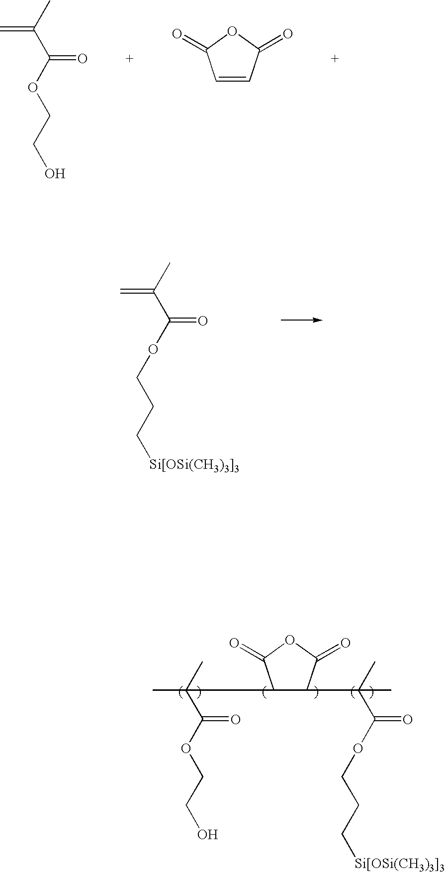
- 2.6 g of 2-hydroxyethyl methacrylate (20 mmol), 2.95 g of maleic anhydride (30 mmol) and 4.3 g of 3-[tris(trimethylsilyloxy)silyl]propyl methacrylate (10 mmol) were dissolved in 20 g of THF and 0.20 g of AIBN (2 mol %), followed by polymerizing, thereby synthesizing a desired polymer at a yield of about 50%.
- The obtained product had a weight average molecular weight (Mw) of about 9,700 and polydispersity (Mw/Mn) of about 1.9.
-

- 4.3 g of 3-[tris(trimethylsilyloxy)silyl]propyl methacrylate (10 mmol) and 5.7 g of glycidyl methacrylate (40 mmol) were dissolved in a round bottom flask containing 40 g of THF and 0.41 g of AIBN (5 mol %) and purged using nitrogen, followed by polymerizing at about 65° C. for about 12 hours.
- After polymerization, the reactant was slowly precipitated with excess n-hexane. Thereafter, the precipitate was filtered, and the filtrate was dissolved in an appropriate amount of THF and re-precipitated in n-hexane. Then, the obtained precipitate was dried in a vacuum oven at about 50° C. for about 24 hours, giving a desired product at a yield of about 75%.
- The obtained product had a weight average molecular weight (Mw) of about 13,500 and polydispersity (Mw/Mn) of about 2.0.
-
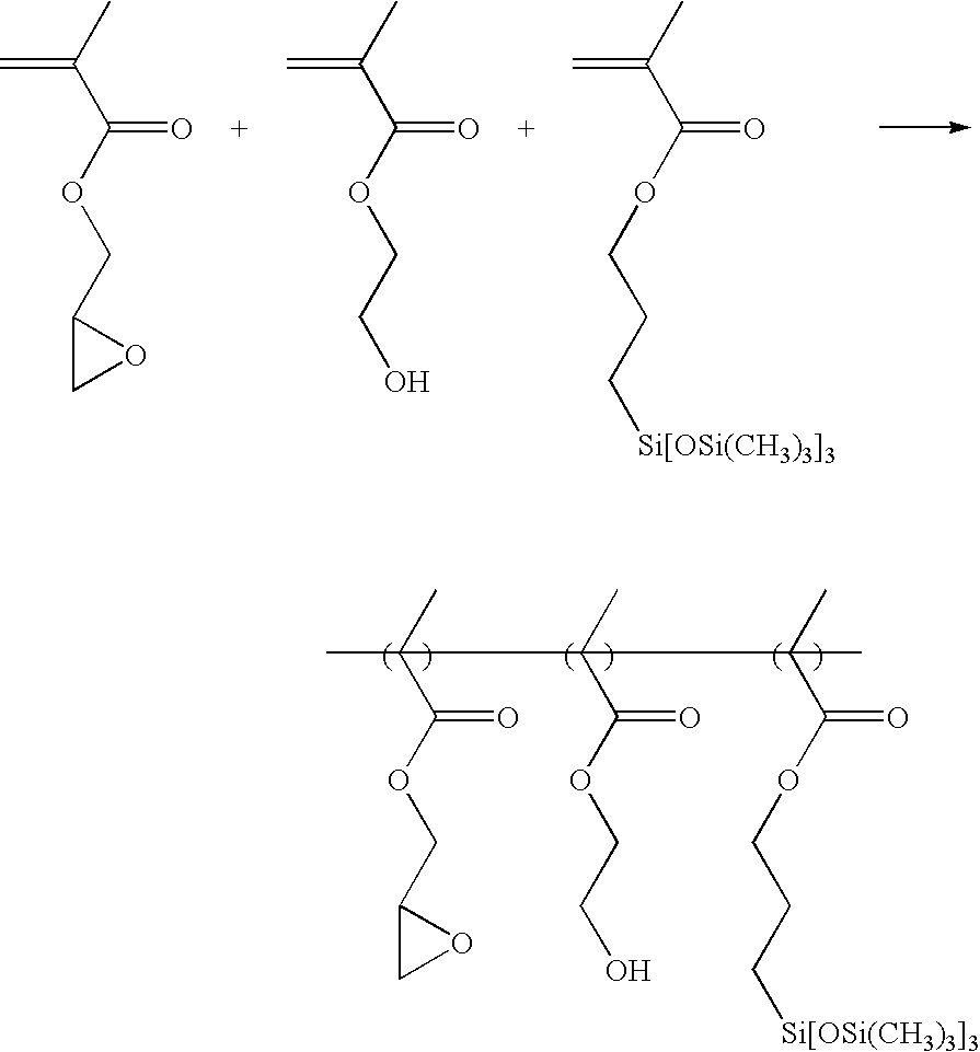
- 2.2 g of glycidyl methacrylate (15 mmol), 2.0 g of 2-hydroxyethyl methacrylate (15 mmol) and 4.3 g of 3-[tris(trimethylsilyloxy)silyl]propyl methacrylate (10 mmol) were dissolved in 30 g of THF and 0.33 g of AIBN (5 mol %), followed by polymerizing in the same manner as in Example 4, thereby synthesizing a desired polymer at a yield of about 70%.
- The obtained product had a weight average molecular weight (Mw) of about 14,100 and polydispersity (Mw/Mn) of about 2.0.
-

- 4.4 g of glycidyl methacrylate (30 mmol), 3.95 g of maleic anhydride (40 mmol) and 4.3 g of 3-[tris(trimethylsilyloxy)silyl]propyl methacrylate (10 mmol) were dissolved in 25 g of THF together with 0.26 g of AIBN (2 mol %), followed by polymerizing in the same manner as in Example 1, thereby synthesizing a desired polymer at a yield of about 50%.
- The obtained product had a weight average molecular weight (Mw) of about 9,100 and polydispersity (Mw/Mn) of about 1.9.
- Using polymers synthesized in Examples 1 through 3 as base polymers, 1.0 g of each polymer, 0.2 g of trimethylolpropane triglycidyl ether as a crosslinking agent, 0.02 g of triphenylsulfonium trifluoromethane sulfonate (triflate) as a PAG and 1 mg triisobutylamine as an organic base were completely dissolved in 10 g of propylene glycol monomethyl ether acetate (PGMEA) and then filtered using a 0.2 μm membrane filter, thereby forming each resist solution. The filtered solution was then coated to a thickness of about 0.25 μm on a bare silicon (Si) wafer treated with hexamethyldisilazane (HMDS), a pre-bake (or soft-bake) was performed at about 120° C. for about 90 seconds and exposed to light using an ArF stepper (0.6 NA, σ=0.75).
- Then, a post exposure bake (PEB) was performed at a temperature of about 120° C. for about 60 seconds. The resultant was developed using a solution of 2.38 wt % tetramethylammonium hydroxide (TMAH) for about 60 seconds. Thus, a 150 nm line-and-space pattern was obtained at an exposure dose of about 11 to about 15 mJ/cm 2.
- Using polymers synthesized in Examples 1 through 3 as base polymers, 1.0 g of each polymer, 0.2 g triglycidyl isocyanurate as a crosslinking agent and 0.02 g triphenylsulfonium trifluoromethane sulfonate (triflate) as a PAG were completely dissolved in 10 g PGMEA and then filtered using a 0.2 μm membrane filter, thereby forming each resist solution. The filtered solution was coated to a thickness of about 0.25 μm on a bare silicon (Si) wafer treated with HMDS, a soft-bake was performed at about 120° C. for about 90 seconds, and then exposed to light using an ArF stepper (0.6 NA, σ=0.75).
- Next, a PEB was performed at a temperature of about 120° C. for about 60 seconds. The resultant was developed using a solution of TMAH (2.38 wt %) for about 60 seconds. Thus, a 150 nm line-and-space pattern was obtained at an exposure dose of about 10 to about 16 mJ/cm 2.
- 1.0 g of each of the respective polymers synthesized in Examples 4 and 6 as a base polymer, 0.2 g of 1,3,5-tris(2-hydroxyethyl)cyanuric acid as a crosslinking agent and 0.02 g of triphenylsulfonium triflate as a PAG were completely dissolved in 10.0 g of propylene glycol monomethyl ether acetate (PGMEA) and then filtered using a 0.2 μm membrane filter, thereby forming each resist solution.
- A resist solution was then coated to a thickness of about 0.25 μm on a silicon (Si) wafer treated with HMDS, and pre-baked at about 120° C. for about 90 seconds, followed by exposing to light using an ArF stepper (0.6NA, σ=0.75). Thereafter, a post exposure bake (PEB) was performed at a temperature of about 120° C. for about 60 seconds.
- The resultant was developed using a solution of TMAH (2.38 wt %) for about 60 seconds. Thus, a 150 nm line-and-space pattern was obtained at an exposure dose of about 11 to about 15 mJ/cm 2.
- 1.0 g of a polymer synthesized in Example 5 as a base polymer, 0.2 g of 1,3,5-tris(2-hydroxyethyl)cyanuric acid as a crosslinking agent, triisobutylamine amine as an organic solvent and 0.02 g of triphenylsulfonium triflate as a PAG were completely dissolved in 10.0 g of propylene glycol monomethyl ether acetate (PGMEA) and then filtered using a 0.2 μm membrane filter, thereby forming a resist solution.
- The resist solution was then coated to a thickness of about 0.25 μm on a silicon (Si) wafer treated with HMDS, and pre-baked at about 120° C. for about 90 seconds, followed by exposure to light using an ArF stepper (0.6NA, σ=0.75).
- Thereafter, a post exposure bake (PEB) was performed at a temperature of about 120° C. for about 60 seconds. The resultant was developed using a solution of TMAH (2.38 wt %) for about 60 seconds. Thus, a 140 nm line-and-space pattern was obtained at an exposure dose of about 10 to about 16 mJ/cm 2.
- A silicon nitride layer is formed on a Si wafer to a thickness of about 3000 Å and an i-line resist (such as ip3300 manufactured by Tokyo Ohka Kogyo Co.) was coated thereon to a thickness of about 500 nm, followed by thermally treating the Si wafer having the silicon nitride layer and i-line resist at a temperature of about 220° C., thereby forming a bottom layer.
- The resist composition (Example 4) obtained from the polymer synthesized in Example 3 was coated on the bottom layer to a thickness of about 250 nm to form a top layer. Thereafter, a soft-bake was performed at about 120° C. for about 90 seconds. Then, an exposure process was performed using an ArF stepper (0.6NA, σ=0.75). Next, a post exposure bake (PEB) was performed at a temperature of about 120° C. for about 60 seconds. The resultant was then developed using a solution of TMAH (2.38 wt %) for about 60 seconds. Next, a post-development bake (PDB) was performed at about 110° C. for about 60 seconds to form a top layer pattern.
- The bottom layer was etched by a dry etching process using O 2 plasma (source gases: O2/SO2) and the top layer pattern as an etching mask to form a bottom layer pattern. Thereafter, the top layer pattern was removed using a stripper.
- Thereafter, a silicon nitride layer was etched by a dry etching process using a CF 4 plasma and the bottom layer pattern comprised of i-line resist as an etching mask, thereby forming a silicon nitride layer pattern. Then, the resist layer remaining on the wafer was removed using a stripper.
- Although the present invention has been particularly shown and described with reference to specific embodiments thereof, the non-limiting embodiments described in the specification of the invention are illustrative only.
- For example, in the manufacture of a negative type resist composition according to the present invention, the crosslinking agent is not limited to the compounds illustrated in the embodiments. For example, as in Examples 7 and 8, triglycidyl isocyanurate, trimethylolpropane triglycidyl ether or triphenylolmethane triglycidyl ether can also be used as a crosslinking agent. Also, as in Examples 9 and 10, 1,3,5-tris(2-hydroxyethyl)cyanuric acid, 1,1,1-tris(hydroxymethyl)ethane, triethylene glycol, diethylene glycol, 1,2,6-trihydroxyhexane, or trimethylolpropane can also be used as a crosslinking agent.
- The PAG is used in an amount of about 1.0 to about 15% by weight based on the weight of the base polymer and examples thereof include triarylsulfonium salts, diaryliodonium salts and mixtures thereof. Also, the organic base is contained in an amount of about 0.01 to about 2.0 wt % on the basis of the total weight of the base polymer and comprises a tertiary amine exemplified by triethylamine, triisobutylamine, trioctylamine, triisodecylamine, diethanolamine, triethanolamine, or mixtures thereof.
- In the patterning described in Examples 7 through 11, during coating, the thickness of the negative type resist composition coated on the wafer may vary according to use. Preferably, the thickness of the negative type resist composition is about 0.2 to about 0.7 μm. Soft-baking is generally performed at about 110 to about 140° C. for about 60 to about 90 seconds. During exposure, an exposure dose may vary according to a deep-UV used. In the case of using ArF or F 2 eximer laser, energy of about 5 to about 100 mJ/cm2 is generally used. The PEB is generally performed at about 100 to about 130° C. for about 60 to about 90 seconds. The development is generally performed using a 2.38 wt % TMAH (0.26N) solution for about 20 to about 60 seconds.
- According to at least one embodiment of the present invention, a polymer comprising a first repeating unit having a Si-containing monomer unit is provided. The polymer further comprises a second repeating unit having a hydroxy group copolymerized with the first repeating unit. The second repeating unit may be a monomer unit having a hydroxy group or a monomer unit having an epoxy ring. The polymer having the above-described structure exhibits high transmittance at short wavelengths and provides high dry etching resistance by including silicon therein. Therefore, the polymer can be used for the manufacture of the negative type resist composition that is advantageously used in forming fine patterns.
- Also, the negative type resist composition according to the present invention includes an alkali soluble base polymer having a repeating unit formed of a Si-containing monomer unit, a PAG and a crosslinking agent. If the base polymer includes a Si-containing monomer unit and a monomer unit having an epoxy ring, the crosslinking agent is formed of a compound having a hydroxy group. Therefore, in the case of using the negative type resist composition according to the embodiments of the present invention in a BLR process, the density of a resist layer is increased by cross-linkage. Therefore, shrinkage caused by e-beam, which is the most serious problem with conventional positive type chemically amplified resists, is prevented. Also, compared with the conventional positive type resist composition, a negative type resist composition according to the present invention has improved adhesion to underlying layers and easily adjustably wettability.
- Further, the negative type resist composition according to the embodiments of the present invention exhibits high transmittance at short wavelengths such as a KrF (248 nm), ArF (193 nm), or F 2 (157 nm) eximer laser, and provides high dry etching resistance by including silicon therein. Therefore, the negative type resist composition can be advantageously used in a BLR process. Also, patterns having large aspect ratios, which are required for highly integrated semiconductor devices, can be formed using the BLR process in conjunction with the negative type resist compositions, according to the embodiments of the present invention.
- While this invention has been particularly shown and described with reference to preferred embodiments thereof, it will be understood by those skilled in the art that various changes in form and details may be made therein without departing from the spirit and scope of the invention.
Claims (63)


Applications Claiming Priority (2)
| Application Number | Priority Date | Filing Date | Title |
|---|---|---|---|
| KR1020020070867A KR100564565B1 (en) | 2002-11-14 | 2002-11-14 | Silicon-containing polymer, negative type resist composition comprising the same, and patterning method for semiconductor device using the same |
| KR2002-70867 | 2002-11-14 |
Publications (2)
| Publication Number | Publication Date |
|---|---|
| US20040106064A1 true US20040106064A1 (en) | 2004-06-03 |
| US7129015B2 US7129015B2 (en) | 2006-10-31 |
Family
ID=32388187
Family Applications (1)
| Application Number | Title | Priority Date | Filing Date |
|---|---|---|---|
| US10/702,778 Expired - Fee Related US7129015B2 (en) | 2002-11-14 | 2003-11-06 | Silicon-containing polymer, negative type resist composition comprising the same, and patterning method for semiconductor device using the same |
Country Status (2)
| Country | Link |
|---|---|
| US (1) | US7129015B2 (en) |
| KR (1) | KR100564565B1 (en) |
Cited By (13)
| Publication number | Priority date | Publication date | Assignee | Title |
|---|---|---|---|---|
| US20070077768A1 (en) * | 2005-09-29 | 2007-04-05 | Tokyo Electron Limited | Substrate processing method |
| US20080044970A1 (en) * | 2006-08-18 | 2008-02-21 | Promos Technologies Inc. | Memory structure and method for preparing the same |
| EP1834969A3 (en) * | 2006-03-07 | 2008-03-26 | National Starch and Chemical Investment Holding Corporation | Curable materials containing siloxane |
| US20100086870A1 (en) * | 2008-10-02 | 2010-04-08 | Shin-Etsu Chemical Co., Ltd. | Composition for forming silicon-containing film, silicon-containing film-formed substrate and patterning process |
| EP2602661A1 (en) * | 2011-12-09 | 2013-06-12 | Shin-Etsu Chemical Co., Ltd. | Chemically amplified negative resist composition, photo-curable dry film, making method, pattern forming process, and electric/electronic part protecting film |
| CN103809375A (en) * | 2012-11-09 | 2014-05-21 | 盖伦奇普有限公司 | Photosensitive resin composition |
| JP2016188987A (en) * | 2015-03-30 | 2016-11-04 | 日立化成株式会社 | Photosensitive resin composition, photosensitive element, semiconductor device and method for forming resist pattern |
| WO2017056928A1 (en) * | 2015-09-30 | 2017-04-06 | 富士フイルム株式会社 | Resist composition, resist film in which same is used, pattern formation method, and method for manufacturing electronic device |
| JP2017107024A (en) * | 2015-12-08 | 2017-06-15 | Jsr株式会社 | Radiation sensitive resin composition, method for forming cured article, cured article, semiconductor element and display element |
| JP2018151644A (en) * | 2012-12-27 | 2018-09-27 | 日立化成株式会社 | Photosensitive resin composition, photosensitive film and method for forming resist pattern |
| CN109836885A (en) * | 2019-01-18 | 2019-06-04 | 广州市红太电子科技有限公司 | Liquid photosensitive ink, PCB and preparation method of PCB inner layer plate |
| WO2019200049A1 (en) * | 2018-04-11 | 2019-10-17 | Wisys Technology Foundation, Inc. | Macromolecular sieves from semiconductor membranes for shape-based separation and sensing |
| US12002674B2 (en) * | 2019-04-11 | 2024-06-04 | Wisys Technology Foundation, Inc. | Macromolecular sieves from semiconductor membranes for shape-based separation and sensing |
Families Citing this family (1)
| Publication number | Priority date | Publication date | Assignee | Title |
|---|---|---|---|---|
| KR100652425B1 (en) * | 2005-08-12 | 2006-12-01 | 삼성전자주식회사 | Top coating composition for photoresist and method for forming photoresist pattern |
Citations (5)
| Publication number | Priority date | Publication date | Assignee | Title |
|---|---|---|---|---|
| US4551417A (en) * | 1982-06-08 | 1985-11-05 | Nec Corporation | Method of forming patterns in manufacturing microelectronic devices |
| US5314961A (en) * | 1990-10-11 | 1994-05-24 | Permeable Technologies, Inc. | Silicone-containing polymers, compositions and improved oxygen permeable hydrophilic contact lenses |
| US5674941A (en) * | 1993-04-16 | 1997-10-07 | Lucky Limited | Antifogging abrasion resistant coating composition and synthetic resin article coated therewith |
| US20040009436A1 (en) * | 2002-07-09 | 2004-01-15 | Samsung Electronics Co., Ltd. | Methods for forming resist pattern and fabricating semiconductor device using Si-containing water-soluble polymer |
| US20040197698A1 (en) * | 2001-07-24 | 2004-10-07 | Kentarou Tamaki | Positive type radiosensitive composition and method for forming pattern |
Family Cites Families (6)
| Publication number | Priority date | Publication date | Assignee | Title |
|---|---|---|---|---|
| JPH02170809A (en) * | 1988-12-24 | 1990-07-02 | Nippon Zeon Co Ltd | Negative type resists |
| JP2707785B2 (en) * | 1990-03-13 | 1998-02-04 | 富士通株式会社 | Resist composition and pattern forming method |
| JPH04294355A (en) * | 1991-03-25 | 1992-10-19 | Fujitsu Ltd | Resin composition and method for formation of resist pattern |
| JP3216799B2 (en) * | 1996-11-13 | 2001-10-09 | 松下電工株式会社 | Heat fixing roll |
| US6358675B1 (en) * | 1998-10-02 | 2002-03-19 | 3M Innovative Properties Company | Silicon-containing alcohols and polymers having silicon-containing tertiary ester groups made therefrom |
| JP2002006504A (en) * | 2000-06-19 | 2002-01-09 | Fuji Photo Film Co Ltd | Original plate for planographic printing |
-
2002
- 2002-11-14 KR KR1020020070867A patent/KR100564565B1/en not_active IP Right Cessation
-
2003
- 2003-11-06 US US10/702,778 patent/US7129015B2/en not_active Expired - Fee Related
Patent Citations (5)
| Publication number | Priority date | Publication date | Assignee | Title |
|---|---|---|---|---|
| US4551417A (en) * | 1982-06-08 | 1985-11-05 | Nec Corporation | Method of forming patterns in manufacturing microelectronic devices |
| US5314961A (en) * | 1990-10-11 | 1994-05-24 | Permeable Technologies, Inc. | Silicone-containing polymers, compositions and improved oxygen permeable hydrophilic contact lenses |
| US5674941A (en) * | 1993-04-16 | 1997-10-07 | Lucky Limited | Antifogging abrasion resistant coating composition and synthetic resin article coated therewith |
| US20040197698A1 (en) * | 2001-07-24 | 2004-10-07 | Kentarou Tamaki | Positive type radiosensitive composition and method for forming pattern |
| US20040009436A1 (en) * | 2002-07-09 | 2004-01-15 | Samsung Electronics Co., Ltd. | Methods for forming resist pattern and fabricating semiconductor device using Si-containing water-soluble polymer |
Cited By (25)
| Publication number | Priority date | Publication date | Assignee | Title |
|---|---|---|---|---|
| US7482281B2 (en) * | 2005-09-29 | 2009-01-27 | Tokyo Electron Limited | Substrate processing method |
| US20070077768A1 (en) * | 2005-09-29 | 2007-04-05 | Tokyo Electron Limited | Substrate processing method |
| EP1834969A3 (en) * | 2006-03-07 | 2008-03-26 | National Starch and Chemical Investment Holding Corporation | Curable materials containing siloxane |
| US20080044970A1 (en) * | 2006-08-18 | 2008-02-21 | Promos Technologies Inc. | Memory structure and method for preparing the same |
| US8852844B2 (en) * | 2008-10-02 | 2014-10-07 | Shin-Etsu Chemical Co., Ltd. | Composition for forming silicon-containing film, silicon-containing film-formed substrate and patterning process |
| US20100086870A1 (en) * | 2008-10-02 | 2010-04-08 | Shin-Etsu Chemical Co., Ltd. | Composition for forming silicon-containing film, silicon-containing film-formed substrate and patterning process |
| JP2013140338A (en) * | 2011-12-09 | 2013-07-18 | Shin Etsu Chem Co Ltd | Chemically amplified negative resist composition, photo-curable dry film, manufacturing method thereof, pattern forming method, and electric/electronic part protecting film |
| US8865391B2 (en) | 2011-12-09 | 2014-10-21 | Shin-Etsu Chemical Co., Ltd. | Chemically amplified negative resist composition, photo-curable dry film, making method, pattern forming process, and electric/electronic part protecting film |
| TWI561923B (en) * | 2011-12-09 | 2016-12-11 | Shinetsu Chemical Co | |
| EP2602661A1 (en) * | 2011-12-09 | 2013-06-12 | Shin-Etsu Chemical Co., Ltd. | Chemically amplified negative resist composition, photo-curable dry film, making method, pattern forming process, and electric/electronic part protecting film |
| CN103809375A (en) * | 2012-11-09 | 2014-05-21 | 盖伦奇普有限公司 | Photosensitive resin composition |
| JP2018151644A (en) * | 2012-12-27 | 2018-09-27 | 日立化成株式会社 | Photosensitive resin composition, photosensitive film and method for forming resist pattern |
| JP2020095279A (en) * | 2012-12-27 | 2020-06-18 | 日立化成株式会社 | Photosensitive resin composition, photosensitive film and method for forming resist pattern |
| JP2016188987A (en) * | 2015-03-30 | 2016-11-04 | 日立化成株式会社 | Photosensitive resin composition, photosensitive element, semiconductor device and method for forming resist pattern |
| WO2017056928A1 (en) * | 2015-09-30 | 2017-04-06 | 富士フイルム株式会社 | Resist composition, resist film in which same is used, pattern formation method, and method for manufacturing electronic device |
| JPWO2017056928A1 (en) * | 2015-09-30 | 2018-01-18 | 富士フイルム株式会社 | Resist composition, and resist film, pattern forming method, and electronic device manufacturing method using the same |
| US10551739B2 (en) | 2015-09-30 | 2020-02-04 | Fujifilm Corporation | Resist composition, and resist film, pattern forming method, and method for manufacturing electronic device, each using resist composition |
| KR20170067649A (en) * | 2015-12-08 | 2017-06-16 | 제이에스알 가부시끼가이샤 | Radiation-sensitive resin composition, method for forming cured film, cured film, semiconductor device, and display device |
| JP2017107024A (en) * | 2015-12-08 | 2017-06-15 | Jsr株式会社 | Radiation sensitive resin composition, method for forming cured article, cured article, semiconductor element and display element |
| KR102554059B1 (en) * | 2015-12-08 | 2023-07-11 | 제이에스알 가부시끼가이샤 | Radiation-sensitive resin composition, method for forming cured film, cured film, semiconductor device, and display device |
| WO2019200049A1 (en) * | 2018-04-11 | 2019-10-17 | Wisys Technology Foundation, Inc. | Macromolecular sieves from semiconductor membranes for shape-based separation and sensing |
| US20210166938A1 (en) * | 2018-04-11 | 2021-06-03 | Wisys Technology Foundation, Inc. | Macromolecular sieves from semiconductor membranes for shape-based separation and sensing |
| CN109836885A (en) * | 2019-01-18 | 2019-06-04 | 广州市红太电子科技有限公司 | Liquid photosensitive ink, PCB and preparation method of PCB inner layer plate |
| CN109836885B (en) * | 2019-01-18 | 2021-10-29 | 广州市红太电子科技有限公司 | Liquid photosensitive ink, PCB and preparation method of PCB inner layer plate |
| US12002674B2 (en) * | 2019-04-11 | 2024-06-04 | Wisys Technology Foundation, Inc. | Macromolecular sieves from semiconductor membranes for shape-based separation and sensing |
Also Published As
| Publication number | Publication date |
|---|---|
| US7129015B2 (en) | 2006-10-31 |
| KR100564565B1 (en) | 2006-03-28 |
| KR20040042916A (en) | 2004-05-22 |
Similar Documents
| Publication | Publication Date | Title |
|---|---|---|
| US7361447B2 (en) | Photoresist polymer and photoresist composition containing the same | |
| US6245482B1 (en) | Polymer and chemically amplified resist composition including silicon containing protecting group | |
| US7226725B2 (en) | Negative resist composition comprising base polymer having epoxy ring and si-containing crosslinker and patterning method for semiconductor device using the same | |
| JP3990146B2 (en) | Photosensitive polymer containing silicon and resist composition containing the same | |
| US7270936B2 (en) | Negative resist composition comprising hydroxy-substituted base polymer and Si-containing crosslinker having epoxy ring and a method for patterning semiconductor devices using the same | |
| US7504195B2 (en) | Photosensitive polymer and photoresist composition | |
| US7129015B2 (en) | Silicon-containing polymer, negative type resist composition comprising the same, and patterning method for semiconductor device using the same | |
| US6787287B2 (en) | Photosensitive polymers and resist compositions comprising the photosensitive polymers | |
| US6777162B2 (en) | Photosensitive polymer and photoresist composition thereof | |
| US6964839B1 (en) | Photosensitive polymer having cyclic backbone and resist composition containing the same | |
| US20030215758A1 (en) | Photosensitive polymer and chemically amplified resist composition comprising the same | |
| US7081325B2 (en) | Photoresist polymer and photoresist composition including the same | |
| US6833230B2 (en) | Photosensitive polymers containing adamantylalkyl vinyl ether, and resist compositions including the same | |
| KR100564643B1 (en) | Silicon-containing polymer, negative type resist composition comprising the same, and patterning method for semiconductor device using the same | |
| KR100536594B1 (en) | A photosensitive polymer containing silicon and resist compositions using the same | |
| US20030224289A1 (en) | Photosensitive polymers and resist compositions containing the same | |
| US6835529B2 (en) | Polymer having butadiene sulfone repeating unit and resist composition comprising the same | |
| KR100604802B1 (en) | Photosensitive polymer having naphthalene derivative in its backbone and resist composition comprising the same | |
| KR20030057948A (en) | Photosensitive polymer having fluorinated-alkyl norbornene carboxylate including hydroxy group and resist composition containing the same | |
| KR20050003604A (en) | Photoresist Composition | |
| KR20000061198A (en) | Resist composition having silicon-containing photosensitive polymer | |
| KR20030028988A (en) | Fluorine-containing photosensitive polymer and chemically amplified positive resist composition comprising the same |
Legal Events
| Date | Code | Title | Description |
|---|---|---|---|
| AS | Assignment |
Owner name: SAMSUNG ELECTRONICS CO., LTD., KOREA, REPUBLIC OF Free format text: ASSIGNMENT OF ASSIGNORS INTEREST;ASSIGNOR:CHOI, SANG-JUN;REEL/FRAME:014690/0267 Effective date: 20031014 |
|
| FEPP | Fee payment procedure |
Free format text: PAYOR NUMBER ASSIGNED (ORIGINAL EVENT CODE: ASPN); ENTITY STATUS OF PATENT OWNER: LARGE ENTITY Free format text: PAYER NUMBER DE-ASSIGNED (ORIGINAL EVENT CODE: RMPN); ENTITY STATUS OF PATENT OWNER: LARGE ENTITY |
|
| FPAY | Fee payment |
Year of fee payment: 4 |
|
| FPAY | Fee payment |
Year of fee payment: 8 |
|
| FEPP | Fee payment procedure |
Free format text: MAINTENANCE FEE REMINDER MAILED (ORIGINAL EVENT CODE: REM.) |
|
| LAPS | Lapse for failure to pay maintenance fees |
Free format text: PATENT EXPIRED FOR FAILURE TO PAY MAINTENANCE FEES (ORIGINAL EVENT CODE: EXP.); ENTITY STATUS OF PATENT OWNER: LARGE ENTITY |
|
| STCH | Information on status: patent discontinuation |
Free format text: PATENT EXPIRED DUE TO NONPAYMENT OF MAINTENANCE FEES UNDER 37 CFR 1.362 |
|
| FP | Lapsed due to failure to pay maintenance fee |
Effective date: 20181031 |