US20030198039A1 - Liquid crystal display module with an enhanced light guide device - Google Patents
Liquid crystal display module with an enhanced light guide device Download PDFInfo
- Publication number
- US20030198039A1 US20030198039A1 US10/445,848 US44584803A US2003198039A1 US 20030198039 A1 US20030198039 A1 US 20030198039A1 US 44584803 A US44584803 A US 44584803A US 2003198039 A1 US2003198039 A1 US 2003198039A1
- Authority
- US
- United States
- Prior art keywords
- light guide
- light
- guide plate
- end portion
- catching jaw
- Prior art date
- Legal status (The legal status is an assumption and is not a legal conclusion. Google has not performed a legal analysis and makes no representation as to the accuracy of the status listed.)
- Granted
Links
Images


Classifications
-
- G—PHYSICS
- G02—OPTICS
- G02B—OPTICAL ELEMENTS, SYSTEMS OR APPARATUS
- G02B6/00—Light guides; Structural details of arrangements comprising light guides and other optical elements, e.g. couplings
- G02B6/0001—Light guides; Structural details of arrangements comprising light guides and other optical elements, e.g. couplings specially adapted for lighting devices or systems
- G02B6/0011—Light guides; Structural details of arrangements comprising light guides and other optical elements, e.g. couplings specially adapted for lighting devices or systems the light guides being planar or of plate-like form
- G02B6/0081—Mechanical or electrical aspects of the light guide and light source in the lighting device peculiar to the adaptation to planar light guides, e.g. concerning packaging
- G02B6/0086—Positioning aspects
- G02B6/0088—Positioning aspects of the light guide or other optical sheets in the package
-
- G—PHYSICS
- G02—OPTICS
- G02F—OPTICAL DEVICES OR ARRANGEMENTS FOR THE CONTROL OF LIGHT BY MODIFICATION OF THE OPTICAL PROPERTIES OF THE MEDIA OF THE ELEMENTS INVOLVED THEREIN; NON-LINEAR OPTICS; FREQUENCY-CHANGING OF LIGHT; OPTICAL LOGIC ELEMENTS; OPTICAL ANALOGUE/DIGITAL CONVERTERS
- G02F1/00—Devices or arrangements for the control of the intensity, colour, phase, polarisation or direction of light arriving from an independent light source, e.g. switching, gating or modulating; Non-linear optics
- G02F1/01—Devices or arrangements for the control of the intensity, colour, phase, polarisation or direction of light arriving from an independent light source, e.g. switching, gating or modulating; Non-linear optics for the control of the intensity, phase, polarisation or colour
- G02F1/13—Devices or arrangements for the control of the intensity, colour, phase, polarisation or direction of light arriving from an independent light source, e.g. switching, gating or modulating; Non-linear optics for the control of the intensity, phase, polarisation or colour based on liquid crystals, e.g. single liquid crystal display cells
- G02F1/133—Constructional arrangements; Operation of liquid crystal cells; Circuit arrangements
- G02F1/1333—Constructional arrangements; Manufacturing methods
- G02F1/1335—Structural association of cells with optical devices, e.g. polarisers or reflectors
-
- G—PHYSICS
- G02—OPTICS
- G02B—OPTICAL ELEMENTS, SYSTEMS OR APPARATUS
- G02B6/00—Light guides; Structural details of arrangements comprising light guides and other optical elements, e.g. couplings
- G02B6/0001—Light guides; Structural details of arrangements comprising light guides and other optical elements, e.g. couplings specially adapted for lighting devices or systems
- G02B6/0011—Light guides; Structural details of arrangements comprising light guides and other optical elements, e.g. couplings specially adapted for lighting devices or systems the light guides being planar or of plate-like form
- G02B6/0066—Light guides; Structural details of arrangements comprising light guides and other optical elements, e.g. couplings specially adapted for lighting devices or systems the light guides being planar or of plate-like form characterised by the light source being coupled to the light guide
- G02B6/0068—Arrangements of plural sources, e.g. multi-colour light sources
-
- G—PHYSICS
- G02—OPTICS
- G02B—OPTICAL ELEMENTS, SYSTEMS OR APPARATUS
- G02B6/00—Light guides; Structural details of arrangements comprising light guides and other optical elements, e.g. couplings
- G02B6/0001—Light guides; Structural details of arrangements comprising light guides and other optical elements, e.g. couplings specially adapted for lighting devices or systems
- G02B6/0011—Light guides; Structural details of arrangements comprising light guides and other optical elements, e.g. couplings specially adapted for lighting devices or systems the light guides being planar or of plate-like form
- G02B6/0066—Light guides; Structural details of arrangements comprising light guides and other optical elements, e.g. couplings specially adapted for lighting devices or systems the light guides being planar or of plate-like form characterised by the light source being coupled to the light guide
- G02B6/007—Incandescent lamp or gas discharge lamp
- G02B6/0071—Incandescent lamp or gas discharge lamp with elongated shape, e.g. tube
-
- G—PHYSICS
- G02—OPTICS
- G02B—OPTICAL ELEMENTS, SYSTEMS OR APPARATUS
- G02B6/00—Light guides; Structural details of arrangements comprising light guides and other optical elements, e.g. couplings
- G02B6/0001—Light guides; Structural details of arrangements comprising light guides and other optical elements, e.g. couplings specially adapted for lighting devices or systems
- G02B6/0011—Light guides; Structural details of arrangements comprising light guides and other optical elements, e.g. couplings specially adapted for lighting devices or systems the light guides being planar or of plate-like form
- G02B6/0081—Mechanical or electrical aspects of the light guide and light source in the lighting device peculiar to the adaptation to planar light guides, e.g. concerning packaging
- G02B6/0093—Means for protecting the light guide
-
- G—PHYSICS
- G02—OPTICS
- G02F—OPTICAL DEVICES OR ARRANGEMENTS FOR THE CONTROL OF LIGHT BY MODIFICATION OF THE OPTICAL PROPERTIES OF THE MEDIA OF THE ELEMENTS INVOLVED THEREIN; NON-LINEAR OPTICS; FREQUENCY-CHANGING OF LIGHT; OPTICAL LOGIC ELEMENTS; OPTICAL ANALOGUE/DIGITAL CONVERTERS
- G02F1/00—Devices or arrangements for the control of the intensity, colour, phase, polarisation or direction of light arriving from an independent light source, e.g. switching, gating or modulating; Non-linear optics
- G02F1/01—Devices or arrangements for the control of the intensity, colour, phase, polarisation or direction of light arriving from an independent light source, e.g. switching, gating or modulating; Non-linear optics for the control of the intensity, phase, polarisation or colour
- G02F1/13—Devices or arrangements for the control of the intensity, colour, phase, polarisation or direction of light arriving from an independent light source, e.g. switching, gating or modulating; Non-linear optics for the control of the intensity, phase, polarisation or colour based on liquid crystals, e.g. single liquid crystal display cells
- G02F1/133—Constructional arrangements; Operation of liquid crystal cells; Circuit arrangements
- G02F1/1333—Constructional arrangements; Manufacturing methods
- G02F1/1335—Structural association of cells with optical devices, e.g. polarisers or reflectors
- G02F1/1336—Illuminating devices
- G02F1/133615—Edge-illuminating devices, i.e. illuminating from the side
Definitions
- the present invention relates to a liquid crystal display device, and more particularly to a light guide device, and a liquid crystal display module and a liquid crystal display device having the light guide device, which can minimize the flowing of a light guide plate received in a mold frame by improving the structure of the light guide plate of the liquid crystal display device.
- an information processing device has been developed to have a various shape, a various function, and a rapid information processing speed.
- the information processed in the information processing device has an electrical signal.
- a display device In order to confirm the information processed in the information processing device with the naked eye, a display device that is needed.
- liquid crystal display device which is lighter, and smaller than a CRT type display device has been developed.
- the liquid crystal display device now displays a full color spectrum in a high resolution.
- the liquid crystal display device is widely used as a computer monitor, a television receiver, and another display device.
- the liquid crystal display device applies a voltage to a liquid crystal layer to change the molecular arrangement of the liquid crystal layer.
- the liquid crystal display device changes of optical properties in the liquid crystal and uses the modulation of a light by using a liquid crystal cell.
- liquid crystal display devices There are two kinds of liquid crystal display devices: TN (Twisted Nematic) method; and an STN (Super-Twisted Nematic) method. Also they can be grouped to an active matrix display method that uses a switching device and a TN liquid crystal, and a passive matrix display method which uses a STN liquid crystal according to the driving type.
- TN Transmission Nematic
- STN Super-Twisted Nematic
- the active matrix display method is used in a TFT-LCD and drives an LCD by using a TFT as a switch.
- the passive matrix display method does not use any transistor and does not need a complex circuit.
- liquid crystal display devices are grouped to a transmissive liquid crystal display device that uses a backlight and a reflecting liquid crystal display device that uses an exterior light source, according to a method for using a light source
- the transmissive liquid crystal display device using the back light as a light source is relatively heavy and voluminous due to the back light, but is widely used since it does not use an exterior light source and displays independently.
- FIG. 1 is an exploded perspective view schematically showing a conventional liquid crystal display device.
- FIG. 2 is a partial exploded perspective view of the liquid crystal display device shown in FIG. 1.
- the liquid crystal display device 900 has a liquid crystal display module 700 to which an image signals is applied to display the screen, and a front surface case 810 and a rear surface case 820 for receiving the liquid crystal display module 700 .
- the liquid crystal display module 700 has a display unit 710 which includes a liquid crystal display panel for displaying the screen.
- the display unit 710 has a liquid crystal display panel 710 , an integrated printed circuit board 714 , a data side tape carrier package 716 , and a gate side flexible circuit board 718 manufactured by the COF method.
- the liquid crystal display panel 712 has a thin film transistor substrate 712 a , a color filter substrate 712 b , and a liquid crystal layer interposed therebetween (not shown).
- the thin film transistor substrate 712 a is a transparent glass substrate on which thin film transistors are formed in a matrix shape. Data lines are connected to source terminals of the thin film transistors, and gate lines are connected to gate terminals of the thin film transistors. Pixel electrodes of indium tin oxide (ITO), which is a transparent conductive material, are formed on drain terminals.
- ITO indium tin oxide
- the color filter substrate 712 b is attached to the thin film transistor substrate 712 a .
- RGB pixels that pass light through to realize color display is formed on the color filter substrate 712 b by a thin film process.
- a common electrode comprised of ITO is coated on the front surface of the color filter board 712 b.
- a driving signal and a timing signal is applied to the gate line and the data line of the thin film transistor to control the arrangement of the liquid crystal of the liquid crystal display panel 712 and the timing when the liquid crystal is arranged.
- the data side tape carrier package 716 which is a kind of flexible circuit board determining the timing when the data driving signal is applied is attached to the source side of the liquid crystal display panel 712
- the gate side flexible circuit board 718 manufactured by the COF method for determining the time at which the gate driving signal is applied is attached to the gate side of the liquid crystal display panel 712 .
- the integrated printed circuit board 714 for receiving image signals from outside of the liquid crystal display panel 712 and applying driving signal to the gate line and the data line is connected to the data tape carrier package 714 of the data line side of the liquid crystal display panel 712 .
- the integrated printed circuit board 714 has a source portion to which the image signals generated in an exterior information processing device (not shown) such as a computer are applied to provided the data driving signals to the liquid crystal display panel 712 and a gate portion for providing the gate driving signals to the gate line of the liquid crystal display panel 712 .
- the integrated printed circuit board 714 generates the gate driving signals for driving the liquid crystal display device, the data signals, and a plurality of timing signals for applying the signals.
- the gate signals are applied to the gate line of the liquid crystal display panel 712 through the gate side flexible circuit board 718
- the data signals are applied to the data line of the liquid crystal display panel 212 through the data tape carrier package 716 .
- a back light assembly 720 for providing a uniform light to the display unit 710 is provided under the display unit 710 .
- the back light assembly 720 comprises a lamp 722 which is provided on one side of the liquid crystal display module 700 to generate the light.
- the lamp 721 is protected by a lamp cover 722 .
- a light guide plate 724 has a size corresponding to the liquid crystal display panel 712 of the display unit 710 , and is located under the liquid crystal display panel 712 .
- the lamp side of the light guide plate 724 is thicker than the other side, and guides the light generated in the lamp 722 towards the display unit 710 to change the passage of the light.
- a plurality of optical sheets 726 for making the luminance of the light irradiated from the light guide plate 724 and passed towards the liquid crystal display panel 712 uniform are provided above the light guide plate 724 .
- a reflection plate 728 for reflecting the light leaking from the light guide plate 724 to increase the light efficiency is provided under the light guide plate 724 .
- the display unit 710 and the back light assembly 720 is fixed and supported by a mold frame 730 that is a receiving receptacle.
- the mold frame 730 has a box-shape, and the upper surface of the mold frame 730 is open. Namely, the mold frame 730 has four side walls and a bottom, and openings for bending the integrated printed circuit board 714 along the outer side surface of the mold frame 730 and positioning the integrated printed circuit board 714 are formed on the lower surface of the bottom.
- a chassis 740 for bending the integrated printed circuit board 714 of the display unit 710 and the gate tape carrier package 718 outside of the mold frame 730 and fixing the integrated printed circuit board 714 of the display unit 710 and the gate tape carrier package 718 to the bottom surface of the mold frame 730 to prevent the deviation of the display unit is provided.
- the chassis 740 has a box-shape. The upper surface of the chassis 740 is opened to expose the liquid crystal display panel 710 , and the side walls are bent inwardly to cover the upper surface peripheral portion of the liquid crystal display panel 710 .
- first and second catching bosses 731 and 732 integrally formed with the mold frame 730 are formed on the corner portion of the side wall of the side on which the lamp 721 is installed in the receiving space of the mold frame 730 .
- the lamp side corner of the light guide plate 724 received in the mold frame 730 is cut off to form first and second catching jaw 724 a and 724 b.
- FIG. 3 shows the state in which the light guide plate shown in FIG. 2 is received in the mold frame.
- FIG. 4 is a partially enlarged view for showing the fixing structure of the light guide plate shown in FIG. 3 and the mold frame.
- FIG. 5 is a top view for showing the size of the light guide plate shown in FIG. 3.
- the first and second catching jaws 724 a and 724 b are engaged with the first and second catching bosses 731 and 732 . Therefore, even when exterior impacts are applied to the liquid crystal display device 900 , the light guide plate 724 is does not move to the lamp side due to the first and second catching bosses 731 and 732 .
- the side wall of the mold frame 730 is getting thinner to minimize the size of the liquid crystal display device 900 .
- the width of the light guide plate 724 of the end portion of the side of the lamp 721 is identical to the width of the end portion of the opposite end portion. Therefore, it is not easy to sufficiently guarantee the thickness of the first and second catching bosses 731 and 732 which are integrally formed with the mold frame 730 . Therefore, as shown in FIG.
- the catching amount of the first and second catching jaws 724 a and 724 b of the light guide plate 724 and the first and second catching bosses 731 and 732 of the mold frame 730 can not be sufficiently guaranteed, making it difficult to prevent the light guide plate 724 from moving to the side of the lamp 721 .
- the width of the light guide plate 724 is increased by the gap between the light guide plate 724 and the mold frame 730 to guarantee the catching amount, the catching amount of the first and second catching jaws 724 a and 724 b and the first and second catching bosses 731 and 732 can be obtained.
- the thermal expansion space of the light guide plate 724 according to the temperature change and the humidity cannot be guaranteed, deteriorating the folding phenomenon.
- the gap between the light guide plate 724 and the mold frame 730 needs to be sufficient.
- the flowing of the light guide plate 724 can be prevented by protruding a portion of both side surfaces of the light guide plate 724 , forming a boss, and forming a recess at a position which corresponds to the boss on both side wall of the mold frame 730 .
- the present invention has been made to solve the above-mentioned problem, and accordingly it is an object of the present invention to provide a light guide device that can minimize the moving of a light guide plate received in a mold frame by improving the structure of the light guide plate.
- the light guide device receives a light generated from a lamp unit and guiding the light to a display unit for displaying an image.
- a catching jaw is formed by cutting off both corner portions of a first end portion of the light guide device to which the light is inputted from the lamp unit and the width of the first end portion including the catching jaw is wider than the width of a second portion opposite to the first end portion.
- the liquid crystal display module comprises a lamp unit for generating a light, a light guide plate for guiding the light from the lamp unit to a display unit for displaying an image, in which a catching jaw is formed by cutting off both corner portions of a first end portion to which the light from the lamp unit is inputted and the width of the first end portion including the catching jaw is wider than the width of a second end portion opposite to the first end portion, and a mold frame for receiving the lamp unit and the light guide plate, in which a catching boss engaged with the catching jaw formed on both corner portions of the first end portion of the light guide plate for fixing the light guide plate is formed at a position that corresponds to the catching jaw of a bottom surface of the mold frame.
- the liquid crystal display device comprises a back light assembly having a lamp unit for generating a light and a light guide plate for guiding the light from the lamp unit to a display unit for displaying an image, in which a catching jaw is formed by cutting off both corner portions of a first end portion to which the light from the lamp unit is inputted and the width of the first end portion including the catching jaw is wider than the width of a second end portion opposite to the first end portion, a mold frame for receiving the lamp unit and the light guide plate, in which a catching boss engaged with the catching jaw formed on both corner portions of the first end portion of the light guide plate for fixing the light guide plate is formed at a position which corresponds to the catching jaw of a bottom surface of the mold frame, and a top chassis for guiding the position of the display unit and fixing the display unit and the back light assembly to the mold frame by engaging the top chassis with the mold frame so as to be opposite to each other.
- the catching jaw of both corner portions of the first end portion is formed in a slope shape in which the width thereof is narrower on the side of the second end portion opposite to the first end portion.
- the light guide device is a wedge type light guide plate in which the first end portion to which the light is inputted is thicker than the second end portion opposite to the first end portion.
- the catching amount of the catching boss integrally formed with the mold frame and the catching jaw of the light guide plate is remarkably increased between the lamp and the light guide plate. Therefore, the light guide plate is prevented from moving towards the lamp even when exterior impacts are applied to the liquid crystal device. Further, since the catching jaw is formed so as to have a slope shape, the concentration of the light inputted from the lamp is prevented.
- FIG. 1 is an exploded perspective view for schematically showing a conventional liquid crystal display device.
- FIG. 2 is an exploded perspective view for showing the structure of a light guide plate and a mold frame shown in FIG. 1.
- FIG. 3 is a view for showing the state in which the light guide plate shown in FIG. 2 is received in the mold frame.
- FIG. 4 is a partially enlarged view for showing the horizontal fixing structure of the light guide plate and the mold frame shown in FIG. 3.
- FIG. 5 is a top view for showing the size of the light guide plate shown in FIG. 3.
- FIG. 6 is an exploded perspective view for showing a liquid crystal display device according to the first preferred embodiment of the present invention.
- FIG. 7 is a perspective view for showing the structure of a light guide plate and a mold frame of the liquid crystal display device according to the first preferred embodiment of the present invention that are shown in FIG. 6.
- FIG. 8 is a view for showing the state in which the light guide plate according to the first preferred embodiment of the present invention shown in FIG. 7 is received in the mold frame.
- FIG. 9 is a partially enlarged view for showing the fixing structure of the light guide plate according to the first preferred embodiment of the present invention shown in FIG. 8 and the mold frame.
- FIG. 10 is a top view for showing the structure of the light guide plate according to the first preferred embodiment of the present invention shown in FIG. 8.
- FIG. 11 is an exploded perspective view for showing a liquid crystal display device according to the second preferred embodiment of the present invention.
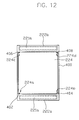
- FIG. 12 is a view for showing the state in which the light guide plate according to the second preferred embodiment of the present invention shown in FIG. 11 is received in a mold frame.
- FIG. 13 is a top view for showing the structure of the light guide plate according to the second preferred embodiment of the present invention shown in FIG. 10.
- FIG. 14 is a top view showing another structure of the light guide plate according to the first preferred embodiment of the present invention shown FIG. 8.
- FIG. 6 is an exploded perspective view for schematically showing a liquid crystal display device according to a first preferred embodiment of the present invention.
- the liquid crystal display device 100 has a liquid crystal display module 200 to which an image signal is applied to display a screen and a case 300 which includes a front case 310 and a rear case 320 for receiving the liquid crystal display module 200 .
- the liquid crystal display module 200 has a display unit 210 having a liquid crystal display panel which displays the screen.
- the display unit 210 has a liquid crystal display panel 212 , an integrated printed circuit board 214 , a data side tape carrier package 216 , and a gate side flexible circuit board 218 manufactured by the COF method.
- the liquid crystal display panel 212 has a thin film transistor substrate 212 a , a color filter substrate 212 b , and a liquid crystal layer interposed therebetween (not shown).
- the thin film transistor substrate 212 a is a transparent glass substrate having a matrix type thin film transistor formed thereon.
- a data line is connected to a source terminal of the thin film transistors, and a gate line is connected to a gate terminal.
- a pixel electrode composed of indium tin oxide (ITO) is formed in a drain terminal.
- the electrical signal is inputted to the data line and the gate line, the electrical signal is inputted to the source terminal and the gate terminal of the thin film transistor.
- the thin film transistor is turned on or off as the gate signal is inputted, and an electrical signal needed to form a pixel image is outputted to the drain terminal.
- the color filter substrate 212 b is opposite to the thin film transistor substrate 212 a .
- the color filter substrate 212 b is a board on which RGB pixels are formed by a thin film process.
- a common electrode of ITO is coated on the front surface of the color filter substrate 212 b.
- the thin film transistor is turned on by applying a power source to the gate terminal and the source terminal of the transistor of the thin film transistor substrate 212 a , an electric field is formed between the pixel electrode and the common electrode of the color filter substrate.
- the arrangement of the liquid crystal injected between the thin film transistor substrate 212 a and the color filter substrate 214 b is changed by the electric field, and light transmission is changed accordingly.
- a driving signal and a timing signal are applied to the gate line and the data line of the thin film transistor.
- the data tape carrier package 216 a flexible circuit board for determining the applying time of a data driving signal, is attached to the source side of the liquid crystal display panel 212 , and the gate side flexible circuit board 218 manufactured by the COF method for determining the applying time of the driving signal of the gate is attached to the gate side.
- the integrated printed circuit board 214 that receives the image signal from outside of the liquid crystal display panel 212 and applies a driving signal to the gate line and the data line is connected to the tape carrier package 214 of the data line side of the liquid crystal display panel 212 .
- a source portion that receives an image signal generated in an exterior information processing device (not shown) and provides a data driving signal to the liquid crystal display panel 212 and a gate portion for providing a gate driving signal to the gate line of the liquid crystal display panel 212 are formed in the integrated printed circuit board 214 .
- the integrated printed circuit board 214 generates the gate driving signal for driving the liquid crystal display device, the data signal, and a plurality of timing signals for applying the signals at a proper time.
- the gate driving signal is applied to the gate line of the liquid crystal display panel 212 through the gate side flexible circuit board 218
- the data signal is applied to the data line of the liquid crystal display panel 212 through the data tape carrier package 216 .
- a back light assembly 220 for providing the display unit 210 with a uniform light is provided under the display unit 210 .
- the back light assembly 220 has a lamp 221 which is provided on one side of the liquid crystal display module 200 to generate a light, and the lamp 221 is protected by a lamp cover 222 .
- a light guide plate 224 has a size corresponding to the liquid crystal panel 212 of the display unit 210 , and guide the light generated in the lamp 221 towards the display unit 210 to change the path of the light.
- a plurality of optical sheets 226 for making the luminance of the light which is irradiated from the light guide plate 224 and is moved towards the liquid crystal display panel 212 uniform are provided above the light guide plate 224 .
- a reflection plate 228 that reflects the light leaking from the light guide plate 224 to increase the efficiency of the light is provided under the light guide plate 224 .
- the display unit 210 and the back light assembly 220 is fixed by a mold frame 400 that is a receptacle assembly.
- FIG. 7 is an exploded perspective view showing the light guide plate and the mold frame of the liquid crystal display device according to the first preferred embodiment of the present invention shown in FIG. 6.
- FIG. 8 is a view showing the state in which the light guide plate according to the first preferred embodiment of the present invention shown in FIG. 7 is received in the mold frame.
- the light guide plate 224 is a wedge type light guide plate in which the thickness thereof becomes thinner as it goes far from the side close to the lamp 221 .
- the first preferred embodiment according to the present invention is applied to the case where the thickness of the both end portions of the light guide plate 224 is identical.
- a first end portion of the light guide plate i.e., both edge portions of the first end portion which is received in a receiving space of the mold frame 400 towards a position at which the lamp 221 is installed is cut off to formed a third catching jaw 224 a and a fourth catching jaw 224 b .
- the overall width of the first end portion in which the third and fourth catching jaws 224 a and 224 b are formed is larger than the width of the second end portion opposite to the first end portion, i.e., the end portion of the far side of the lamp 221 . It is because the catching body is integrally formed with the light guide plate 224 on the side wall of the third and fourth catching jaws 224 a and 224 b , and it will be explained in detail with reference to FIGS. 9 and 10.
- the lamp 221 and the lamp cover 222 are received on one side of the receiving space of the mold frame 400 that receives the light guide plate 224 .
- Third and fourth catching bosses 402 and 404 which are engaged with the third and fourth catching jaw 224 a and 224 b to prevent the flowing of the horizontal direction of the light guide plate 224 are integrally formed with the mold frame 400 in both corner portions of the side wall on which the lamp 221 is positioned.
- Third and fourth catching covers 406 and 408 for preventing the light guide plate 224 received in the mold frame 400 from being deviated to the vertical direction of the receiving space are integrally formed with the mold frame 400 in both corner portions of the side wall opposite to the third and fourth catching bosses 402 and 404 .
- FIG. 9 is a partial enlarged view for showing the fixing structure of the light guide plate and the mold frame according to the first preferred embodiment of the present invention shown in FIG. 8.
- FIG. 10 shows in detail the structure of the light guide plate according to the first preferred embodiment of the present invention shown in FIG. 8.
- the gap between the side surface of the third catching jaw 224 a and the side wall of the mold frame 400 is narrower than the gap between the side surface of the second end portion of the light guide plate 224 and the mold frame 400 . It is because the catching body is integrally formed with the light guide plate 224 on the side wall of the third catching jaw 224 a .
- the catching body has a slope shape in which the width thereof is narrower as it proceeds towards the second end portion.
- the width of the third catching jaw 224 a of the light guide plate 224 is narrower as it proceeds towards the first end portion to the second end portion.
- the catching body is formed in the fourth catching jaw 224 b . Therefore, the catching amount between the third and fourth catching jaws 224 a and 224 b and the third and fourth catching bosses 402 and 404 is increased by the width of the catching body.
- the widths W 3 and W 4 of the third and fourth catching jaws 224 a and 224 b of the light guide plate 224 are identical before the catching bodies 224 a ′ and 224 b ′ are attached to the third and fourth catching jaws 224 a and 224 b .
- the widths of the first end portion and the second end portion are identical.
- the width W 1 ′ of the first end portion increases by the widths W 5 and W 6 of the catching bodies 224 a ′ and 224 b ′ in relation to the width W 2 of the second end portion. Therefore, as shown in FIG. 9, the catching amount between the third and fourth catching jaws 224 a and 224 b and the third and fourth catching bosses 402 and 404 are sufficiently obtained, and thus the light guide plate 224 is prevented from being flowed towards the lamp 221 by the exterior impacts.
- the catching bodies 224 a ′ and 224 b ′ has a slope shape in which the width thereof is narrower as it proceeds towards the second end portion, the concentration of the light irradiated from the lamp 221 is prevented. Since the gap between the light guide plate 224 and the side wall of the mold frame 400 except for the portion in which the catching bodies 224 a ′ and 224 b ′ are attached is sufficiently maintained, the folding of the light guide plate 224 according to the temperature and the humidity is prevented.
- FIG. 11 is an exploded perspective view showing the liquid crystal display device according to the second preferred embodiment of the present invention.
- the liquid crystal display device according to the second preferred embodiment of the present invention has the same structure as the liquid crystal display device according to the first preferred embodiment of the present invention shown in FIG. 6 except for a back light assembly 220 and a back cover 400 a .
- the liquid crystal display device according to the second preferred embodiment of the present invention shown in FIG. 11 has a monitor device which employs two lamps.
- a back light assembly 220 for providing the uniform light to the display unit 210 is provided under the display unit 210 .
- the back light assembly 220 has first and second lamps 221 a and 221 b which are provided on both sides of the liquid crystal display module 220 to generate the light, and the first and second lamps 221 a and 221 b are protected by the first and second lamp covers 222 a and 222 b .
- the light guide plate 224 has a size which corresponds to the liquid crystal panel 212 of the display unit 210 , and guides the light generated from the first and second lamps 221 a and 221 b towards the display unit 210 to change the path of the light.
- the light guide plate 224 can be a plurality of light guide plates, and can be a single light guide plate.
- the display unit 210 and the back light assembly 220 are supported by the mold frame which is a receiving receptacle assembly.
- a back cover 400 a made of metal for interrupting and reducing EMI generated in the monitor device is engaged with the rear surface of the mold frame 400 .
- FIG. 12 shows the state in which the light guide plate according to the second preferred embodiment of the present invention shown in FIG. 11 is received in the mold frame.
- FIG. 13 is a top view for showing the structure of the light guide plate according to the second preferred embodiment of the present invention shown in FIG. 10.
- the first end of the light guide plate 224 i.e., both corner portion of the first end portion which is opposite to the side wall in which the first lamp 221 a is installed in the receiving space of the mold frame is cut off to form a fifth catching jaw 224 a and a sixth catching jaw 224 b .
- the second end portion opposite to the first end portion of the light guide plate 224 i.e., both corner portions of the second end portion opposite to the side wall in which the second lamp 221 b is installed in the receiving space of the mold frame 400 is cut off to form a seventh catching jaw 224 c and an eighth catching jaw 224 d.
- the total width W 1 ′ of the first end portion in which the fifth and sixth catching jaws 224 a and 224 b are formed is identical to the width W 2 ′ of the second end portion in which the seventh and eighth catching jaws 224 c and 224 d are formed.
- the catching bodies 224 a ′, 224 b ′, 224 c ′, and 224 d ′ are integrally formed with the side surfaces of the fifth, sixth, seventh, and eighth catching jaws 224 a , 224 b , 224 c , and 224 d , and the overall width of the first and second end portions is wider than the width W 7 of the central portion of the light guide plate 224 . It will be explained in detail with reference to FIG. 13.
- the first lamp 221 a and the first lamp cover 222 a are received on the side opposite to the first end portion of the light guide plate 224 and the second lamp 221 b and the second lamp cover 222 b are received on the side opposite to the second end portion.
- Fifth and sixth catching bosses 402 and 404 which are engaged with the fifth and six catching jaws 224 a and 224 b to prevent the flowing of the light guide plate 224 towards the first lamp 221 a are integrally formed with the mold frame 400 on both corner portions of the side wall in which the first lamp 221 a is positioned.
- Seventh and eighth catching bosses 406 and 408 which are engaged with the seventh and eighth catching jaws 224 c and 224 d to prevent the flowing of the light guide plate 224 towards the second lamp 221 b are integrally formed with the mold frame 400 on both corner portions of the side wall in which the second lamp 221 b is positioned.
- the fifth catching jaw 224 a and the fifth catching boss 402 , the six the catching jaw 224 b and the sixth catching boss 404 , the seventh catching jaw 224 c and the seventh catching boss 406 , and the eighth catching jaw 224 d and the eighth catching boss 408 are respectively engaged to prevent the horizontal flowing of the light guide plate 224 .
- the gap between the side surface of the fifth catching jaw 224 a and the side wall of the mold frame 400 is narrower than the gap between the side surface of the central portion of the light guide plate 224 and the mold frame 400 . It is because the catching body 224 a ′ is integrally attached to the light guide plate 224 on the side wall of the fifth catching jaw 224 a , and the catching body 224 a ′ has a smooth slope in which the width W 5 thereof is narrower at the central portion of the light guide plate.
- the catching body 224 a ′ is identical in the sixth, seventh, and eighth catching jaws 224 b , 224 c , and 224 d of the light guide plate 224 .
- the catching amount between the fifth, sixth, seventh, and eighth catching jaws 224 a , 224 b , 224 c , and 224 d and the fifth, sixth, seventh, and eighth catching bosses 402 , 404 , 406 , and 408 is respectively increased by the widths W 5 , W 6 , W 5 ′, and W 6 ′ of the catching bodies 224 a ′, 224 b ′, 224 c ′, and 224 d′.
- the widths W 3 , W 4 , W 3 ′, and W 4 ′ of the fifth, sixth, seventh, and eighth catching jaws 224 a , 224 b , 224 c , and 224 d are identical before the catching bodies 224 a ′, 224 b ′, 224 c ′, and 224 d ′ are attached to the fifth, sixth, seventh, and eights catching jaws 224 a , 224 b , 224 c , and 224 d .
- the width W 1 ′ of the first end portion and the width W 2 ′ of the second end portion are wider than the width W 7 of the central portion by the widths W 5 and W 6 of the catching bodies 224 a ′ and 224 b ′. Therefore, as shown in FIG.
- the catching amounts between the fifth, sixth, seventh, and eighth catching jaws 224 a , 224 b , 224 c , and 224 d and the fifth, sixth, seventh, and eighth catching bosses 402 , 404 , 406 , and 408 are sufficiently obtained, and thus the light guide plate 224 is prevented from being flowed towards the first lamp 221 a or the second lamp 221 b by the exterior impacts.
- the catching bodies 224 a ′, 224 b ′, 224 c ′, and 224 d ′ has a slope shape in which the widths W 5 , W 6 , W 5 ′, and W 6 ′ are narrower towards the central portion, the light irradiated from the first and second lamps 221 a and 221 b is prevented from being concentrated.
- the above-mentioned catching body of the light guide plate 224 is also formed at one corner portion of an end portion of the light guide plate 225 .
- a first end portion of the light guide plate 225 i.e., one corner portion of the first end portion which is received in a receiving space of the mold frame 400 toward a position at which the lamp 221 is installed is cut off to form a ninth catching jaw 225 a shaping the same as the third catching jaw 224 a .
- Another corner portion of the first end portion is also cut off to form a catching jaw as shown in FIG. 14 or is formed into a particular shape according to the developing environment of the liquid crystal display device.
- a catching body 225 a ′ is formed on the side wall 225 c of the corner portion at which the ninth catching jaw 225 a is formed.
- the catching body 225 a ′ is formed to elongate from the ninth catching jaw 225 a and have a slope shape in which the width thereof is narrower at the central portion of the light guide plate 225 .
- catching jaws are formed on both corner portions of the end portions opposite to the lamp installed in the mold frame among the side surface of the light guide plate, and the width of the end portion including the catching jaw is wider than the width of the end portion received towards a side on which the lamp is not installed. Further, the outer surface of the catching jaw formed in the both corner portions has a slope shape in which the width thereof is narrower as it proceeds towards the central portion.
- the catching amount of the catching bosses integrally formed with the mold frame and the catching jaws of the light guide plate is remarkably increased. Therefore, the light guide plate is prevented from being flowed towards the lamp even when the exterior impacts are applied to the liquid crystal display device. Further, since the catching jaw is formed in a slope shape, the light irradiated from the lamp is prevented from being concentrated.
Landscapes
- Physics & Mathematics (AREA)
- General Physics & Mathematics (AREA)
- Optics & Photonics (AREA)
- Nonlinear Science (AREA)
- Mathematical Physics (AREA)
- Chemical & Material Sciences (AREA)
- Crystallography & Structural Chemistry (AREA)
- Liquid Crystal (AREA)
- Devices For Indicating Variable Information By Combining Individual Elements (AREA)
- Planar Illumination Modules (AREA)
- Light Guides In General And Applications Therefor (AREA)
- Securing Globes, Refractors, Reflectors Or The Like (AREA)
Abstract
Description
- 1. Field of the Invention
- The present invention relates to a liquid crystal display device, and more particularly to a light guide device, and a liquid crystal display module and a liquid crystal display device having the light guide device, which can minimize the flowing of a light guide plate received in a mold frame by improving the structure of the light guide plate of the liquid crystal display device.
- 2. Description of the Related Art
- Recently, an information processing device has been developed to have a various shape, a various function, and a rapid information processing speed. The information processed in the information processing device has an electrical signal. In order to confirm the information processed in the information processing device with the naked eye, a display device that is needed.
- Recently, a liquid crystal display device which is lighter, and smaller than a CRT type display device has been developed. The liquid crystal display device now displays a full color spectrum in a high resolution. As a result, the liquid crystal display device is widely used as a computer monitor, a television receiver, and another display device.
- The liquid crystal display device applies a voltage to a liquid crystal layer to change the molecular arrangement of the liquid crystal layer. The liquid crystal display device changes of optical properties in the liquid crystal and uses the modulation of a light by using a liquid crystal cell.
- There are two kinds of liquid crystal display devices: TN (Twisted Nematic) method; and an STN (Super-Twisted Nematic) method. Also they can be grouped to an active matrix display method that uses a switching device and a TN liquid crystal, and a passive matrix display method which uses a STN liquid crystal according to the driving type.
- The active matrix display method is used in a TFT-LCD and drives an LCD by using a TFT as a switch. The passive matrix display method does not use any transistor and does not need a complex circuit.
- Further, liquid crystal display devices are grouped to a transmissive liquid crystal display device that uses a backlight and a reflecting liquid crystal display device that uses an exterior light source, according to a method for using a light source The transmissive liquid crystal display device using the back light as a light source is relatively heavy and voluminous due to the back light, but is widely used since it does not use an exterior light source and displays independently.
- FIG. 1 is an exploded perspective view schematically showing a conventional liquid crystal display device. FIG. 2 is a partial exploded perspective view of the liquid crystal display device shown in FIG. 1.
- Referring to FIG. 1, the liquid
crystal display device 900 has a liquidcrystal display module 700 to which an image signals is applied to display the screen, and afront surface case 810 and arear surface case 820 for receiving the liquidcrystal display module 700. - The liquid
crystal display module 700 has adisplay unit 710 which includes a liquid crystal display panel for displaying the screen. - The
display unit 710 has a liquidcrystal display panel 710, an integratedprinted circuit board 714, a data sidetape carrier package 716, and a gate sideflexible circuit board 718 manufactured by the COF method. - The liquid
crystal display panel 712 has a thinfilm transistor substrate 712 a, acolor filter substrate 712 b, and a liquid crystal layer interposed therebetween (not shown). - The thin
film transistor substrate 712 a is a transparent glass substrate on which thin film transistors are formed in a matrix shape. Data lines are connected to source terminals of the thin film transistors, and gate lines are connected to gate terminals of the thin film transistors. Pixel electrodes of indium tin oxide (ITO), which is a transparent conductive material, are formed on drain terminals. - If electrical signals are inputted to the data lines and the gate lines, the electrical signals are inputted to the source terminals and the gate terminals of thin film transistors and the thin film transistors are turned on or off so that electrical signals for forming pixels are outputted to the drain terminals.
- The
color filter substrate 712 b is attached to the thinfilm transistor substrate 712 a. RGB pixels that pass light through to realize color display is formed on thecolor filter substrate 712 b by a thin film process. A common electrode comprised of ITO is coated on the front surface of thecolor filter board 712 b. - If power sources are applied to the gate terminals and the source terminals of the transistors and the thin film transistors are turned on, an electric field is formed between the pixel electrode on the thin film transistor substrate and the common electrode on the color filter substrate. The arrangement angles of the liquid crystals injected between the thin
film transistor board 712 a and the color filter board 714 b changes by the electric field, and the light passage changes due to the arrangement angle changes to obtain a desired pixel status. - A driving signal and a timing signal is applied to the gate line and the data line of the thin film transistor to control the arrangement of the liquid crystal of the liquid
crystal display panel 712 and the timing when the liquid crystal is arranged. The data sidetape carrier package 716 which is a kind of flexible circuit board determining the timing when the data driving signal is applied is attached to the source side of the liquidcrystal display panel 712, and the gate sideflexible circuit board 718 manufactured by the COF method for determining the time at which the gate driving signal is applied is attached to the gate side of the liquidcrystal display panel 712. - The integrated
printed circuit board 714 for receiving image signals from outside of the liquidcrystal display panel 712 and applying driving signal to the gate line and the data line is connected to the datatape carrier package 714 of the data line side of the liquidcrystal display panel 712. The integrated printedcircuit board 714 has a source portion to which the image signals generated in an exterior information processing device (not shown) such as a computer are applied to provided the data driving signals to the liquidcrystal display panel 712 and a gate portion for providing the gate driving signals to the gate line of the liquidcrystal display panel 712. Namely, the integratedprinted circuit board 714 generates the gate driving signals for driving the liquid crystal display device, the data signals, and a plurality of timing signals for applying the signals. The gate signals are applied to the gate line of the liquidcrystal display panel 712 through the gate sideflexible circuit board 718, and the data signals are applied to the data line of the liquidcrystal display panel 212 through the datatape carrier package 716. - A
back light assembly 720 for providing a uniform light to thedisplay unit 710 is provided under thedisplay unit 710. Theback light assembly 720 comprises alamp 722 which is provided on one side of the liquidcrystal display module 700 to generate the light. Thelamp 721 is protected by alamp cover 722. Alight guide plate 724 has a size corresponding to the liquidcrystal display panel 712 of thedisplay unit 710, and is located under the liquidcrystal display panel 712. The lamp side of thelight guide plate 724 is thicker than the other side, and guides the light generated in thelamp 722 towards thedisplay unit 710 to change the passage of the light. - A plurality of
optical sheets 726 for making the luminance of the light irradiated from thelight guide plate 724 and passed towards the liquidcrystal display panel 712 uniform are provided above thelight guide plate 724. Areflection plate 728 for reflecting the light leaking from thelight guide plate 724 to increase the light efficiency is provided under thelight guide plate 724. - The
display unit 710 and theback light assembly 720 is fixed and supported by amold frame 730 that is a receiving receptacle. Themold frame 730 has a box-shape, and the upper surface of themold frame 730 is open. Namely, themold frame 730 has four side walls and a bottom, and openings for bending the integrated printedcircuit board 714 along the outer side surface of themold frame 730 and positioning the integrated printedcircuit board 714 are formed on the lower surface of the bottom. - A
chassis 740 for bending the integratedprinted circuit board 714 of thedisplay unit 710 and the gatetape carrier package 718 outside of themold frame 730 and fixing the integrated printedcircuit board 714 of thedisplay unit 710 and the gatetape carrier package 718 to the bottom surface of themold frame 730 to prevent the deviation of the display unit is provided. Thechassis 740 has a box-shape. The upper surface of thechassis 740 is opened to expose the liquidcrystal display panel 710, and the side walls are bent inwardly to cover the upper surface peripheral portion of the liquidcrystal display panel 710. - On the other hand, referring to FIG. 2, first and second catching
bosses mold frame 730 are formed on the corner portion of the side wall of the side on which thelamp 721 is installed in the receiving space of themold frame 730. The lamp side corner of thelight guide plate 724 received in themold frame 730 is cut off to form first and second catchingjaw - FIG. 3 shows the state in which the light guide plate shown in FIG. 2 is received in the mold frame. FIG. 4 is a partially enlarged view for showing the fixing structure of the light guide plate shown in FIG. 3 and the mold frame. FIG. 5 is a top view for showing the size of the light guide plate shown in FIG. 3.
- Referring to FIG. 3, if the
light guide plate 724 is received in themold frame 730, the first and second catchingjaws bosses crystal display device 900, thelight guide plate 724 is does not move to the lamp side due to the first and secondcatching bosses - However, recently, the side wall of the
mold frame 730 is getting thinner to minimize the size of the liquidcrystal display device 900. Further, as shown in FIG. 5, the width of thelight guide plate 724 of the end portion of the side of thelamp 721 is identical to the width of the end portion of the opposite end portion. Therefore, it is not easy to sufficiently guarantee the thickness of the first and secondcatching bosses mold frame 730. Therefore, as shown in FIG. 4, the catching amount of the first and second catchingjaws light guide plate 724 and the first and secondcatching bosses mold frame 730 can not be sufficiently guaranteed, making it difficult to prevent thelight guide plate 724 from moving to the side of thelamp 721. - On the other hand, if the width of the
light guide plate 724 is increased by the gap between thelight guide plate 724 and themold frame 730 to guarantee the catching amount, the catching amount of the first and second catchingjaws bosses light guide plate 724 and themold frame 730, the thermal expansion space of thelight guide plate 724 according to the temperature change and the humidity cannot be guaranteed, deteriorating the folding phenomenon. Especially, in the wedge typelight guide plate 724 shown in FIG. 1, since the thermal expansion rate is large at a portion thelight guide plate 724 is thin, the gap between thelight guide plate 724 and themold frame 730 needs to be sufficient. - On the other hand, even if it is not shown, the flowing of the
light guide plate 724 can be prevented by protruding a portion of both side surfaces of thelight guide plate 724, forming a boss, and forming a recess at a position which corresponds to the boss on both side wall of themold frame 730. However, in the case, it is not easy to guarantee the catching amount between the boss and the recess and the light inputted from the lamp is concentrated at a corner portion bent by the boss and the recess. - The present invention has been made to solve the above-mentioned problem, and accordingly it is an object of the present invention to provide a light guide device that can minimize the moving of a light guide plate received in a mold frame by improving the structure of the light guide plate.
- It is another object of the present invention to provide a liquid crystal display module having a light guide device that can minimize the moving of a light guide plate received in a mold frame by improving the structure of the light guide plate.
- It is another object of the present invention to provide a liquid crystal display device having a light guide device that can minimize the moving of a light guide plate received in a mold frame by improving the structure of the light guide plate.
- The light guide device according to the present invention receives a light generated from a lamp unit and guiding the light to a display unit for displaying an image. A catching jaw is formed by cutting off both corner portions of a first end portion of the light guide device to which the light is inputted from the lamp unit and the width of the first end portion including the catching jaw is wider than the width of a second portion opposite to the first end portion.
- The liquid crystal display module according to the present invention comprises a lamp unit for generating a light, a light guide plate for guiding the light from the lamp unit to a display unit for displaying an image, in which a catching jaw is formed by cutting off both corner portions of a first end portion to which the light from the lamp unit is inputted and the width of the first end portion including the catching jaw is wider than the width of a second end portion opposite to the first end portion, and a mold frame for receiving the lamp unit and the light guide plate, in which a catching boss engaged with the catching jaw formed on both corner portions of the first end portion of the light guide plate for fixing the light guide plate is formed at a position that corresponds to the catching jaw of a bottom surface of the mold frame.
- The liquid crystal display device according to the present invention comprises a back light assembly having a lamp unit for generating a light and a light guide plate for guiding the light from the lamp unit to a display unit for displaying an image, in which a catching jaw is formed by cutting off both corner portions of a first end portion to which the light from the lamp unit is inputted and the width of the first end portion including the catching jaw is wider than the width of a second end portion opposite to the first end portion, a mold frame for receiving the lamp unit and the light guide plate, in which a catching boss engaged with the catching jaw formed on both corner portions of the first end portion of the light guide plate for fixing the light guide plate is formed at a position which corresponds to the catching jaw of a bottom surface of the mold frame, and a top chassis for guiding the position of the display unit and fixing the display unit and the back light assembly to the mold frame by engaging the top chassis with the mold frame so as to be opposite to each other.
- The catching jaw of both corner portions of the first end portion is formed in a slope shape in which the width thereof is narrower on the side of the second end portion opposite to the first end portion.
- The light guide device is a wedge type light guide plate in which the first end portion to which the light is inputted is thicker than the second end portion opposite to the first end portion.
- According to the light guide device, the liquid crystal display module, and the liquid crystal display device according to the present invention, the catching amount of the catching boss integrally formed with the mold frame and the catching jaw of the light guide plate is remarkably increased between the lamp and the light guide plate. Therefore, the light guide plate is prevented from moving towards the lamp even when exterior impacts are applied to the liquid crystal device. Further, since the catching jaw is formed so as to have a slope shape, the concentration of the light inputted from the lamp is prevented.
- The above and other objects and advantages of the present invention will become readily apparent by reference to the following detailed description when considered in conjunction with the accompanying drawings.
- FIG. 1 is an exploded perspective view for schematically showing a conventional liquid crystal display device.
- FIG. 2 is an exploded perspective view for showing the structure of a light guide plate and a mold frame shown in FIG. 1.
- FIG. 3 is a view for showing the state in which the light guide plate shown in FIG. 2 is received in the mold frame.
- FIG. 4 is a partially enlarged view for showing the horizontal fixing structure of the light guide plate and the mold frame shown in FIG. 3.
- FIG. 5 is a top view for showing the size of the light guide plate shown in FIG. 3.
- FIG. 6 is an exploded perspective view for showing a liquid crystal display device according to the first preferred embodiment of the present invention.
- FIG. 7 is a perspective view for showing the structure of a light guide plate and a mold frame of the liquid crystal display device according to the first preferred embodiment of the present invention that are shown in FIG. 6.
- FIG. 8 is a view for showing the state in which the light guide plate according to the first preferred embodiment of the present invention shown in FIG. 7 is received in the mold frame.
- FIG. 9 is a partially enlarged view for showing the fixing structure of the light guide plate according to the first preferred embodiment of the present invention shown in FIG. 8 and the mold frame.
- FIG. 10 is a top view for showing the structure of the light guide plate according to the first preferred embodiment of the present invention shown in FIG. 8.
- FIG. 11 is an exploded perspective view for showing a liquid crystal display device according to the second preferred embodiment of the present invention.
- FIG. 12 is a view for showing the state in which the light guide plate according to the second preferred embodiment of the present invention shown in FIG. 11 is received in a mold frame.
- FIG. 13 is a top view for showing the structure of the light guide plate according to the second preferred embodiment of the present invention shown in FIG. 10.
- FIG. 14 is a top view showing another structure of the light guide plate according to the first preferred embodiment of the present invention shown FIG. 8.
- Hereinafter, preferred embodiments of the present invention will be explained in detail with reference to the attached drawings.
- Embodiment 1
- FIG. 6 is an exploded perspective view for schematically showing a liquid crystal display device according to a first preferred embodiment of the present invention.
- Referring to FIG. 6, the liquid
crystal display device 100 has a liquidcrystal display module 200 to which an image signal is applied to display a screen and acase 300 which includes afront case 310 and arear case 320 for receiving the liquidcrystal display module 200. - The liquid
crystal display module 200 has adisplay unit 210 having a liquid crystal display panel which displays the screen. - The
display unit 210 has a liquidcrystal display panel 212, an integrated printedcircuit board 214, a data sidetape carrier package 216, and a gate sideflexible circuit board 218 manufactured by the COF method. - The liquid
crystal display panel 212 has a thinfilm transistor substrate 212 a, acolor filter substrate 212 b, and a liquid crystal layer interposed therebetween (not shown). - The thin
film transistor substrate 212 a is a transparent glass substrate having a matrix type thin film transistor formed thereon. A data line is connected to a source terminal of the thin film transistors, and a gate line is connected to a gate terminal. A pixel electrode composed of indium tin oxide (ITO) is formed in a drain terminal. - If an electrical signal is inputted to the data line and the gate line, the electrical signal is inputted to the source terminal and the gate terminal of the thin film transistor. The thin film transistor is turned on or off as the gate signal is inputted, and an electrical signal needed to form a pixel image is outputted to the drain terminal.
- The
color filter substrate 212 b is opposite to the thinfilm transistor substrate 212 a. Thecolor filter substrate 212 b is a board on which RGB pixels are formed by a thin film process. A common electrode of ITO is coated on the front surface of thecolor filter substrate 212 b. - If the thin film transistor is turned on by applying a power source to the gate terminal and the source terminal of the transistor of the thin
film transistor substrate 212 a, an electric field is formed between the pixel electrode and the common electrode of the color filter substrate. The arrangement of the liquid crystal injected between the thinfilm transistor substrate 212 a and the color filter substrate 214 b is changed by the electric field, and light transmission is changed accordingly. - In order to control the timing for the arrangement of the liquid crystal of the liquid
crystal display panel 212, a driving signal and a timing signal are applied to the gate line and the data line of the thin film transistor. - As shown, the data
tape carrier package 216, a flexible circuit board for determining the applying time of a data driving signal, is attached to the source side of the liquidcrystal display panel 212, and the gate sideflexible circuit board 218 manufactured by the COF method for determining the applying time of the driving signal of the gate is attached to the gate side. - The integrated printed
circuit board 214 that receives the image signal from outside of the liquidcrystal display panel 212 and applies a driving signal to the gate line and the data line is connected to thetape carrier package 214 of the data line side of the liquidcrystal display panel 212. - A source portion that receives an image signal generated in an exterior information processing device (not shown) and provides a data driving signal to the liquid
crystal display panel 212 and a gate portion for providing a gate driving signal to the gate line of the liquidcrystal display panel 212 are formed in the integrated printedcircuit board 214. - Namely, the integrated printed
circuit board 214 generates the gate driving signal for driving the liquid crystal display device, the data signal, and a plurality of timing signals for applying the signals at a proper time. The gate driving signal is applied to the gate line of the liquidcrystal display panel 212 through the gate sideflexible circuit board 218, and the data signal is applied to the data line of the liquidcrystal display panel 212 through the datatape carrier package 216. - A back
light assembly 220 for providing thedisplay unit 210 with a uniform light is provided under thedisplay unit 210. The backlight assembly 220 has alamp 221 which is provided on one side of the liquidcrystal display module 200 to generate a light, and thelamp 221 is protected by alamp cover 222. Alight guide plate 224 has a size corresponding to theliquid crystal panel 212 of thedisplay unit 210, and guide the light generated in thelamp 221 towards thedisplay unit 210 to change the path of the light. - A plurality of
optical sheets 226 for making the luminance of the light which is irradiated from thelight guide plate 224 and is moved towards the liquidcrystal display panel 212 uniform are provided above thelight guide plate 224. Areflection plate 228 that reflects the light leaking from thelight guide plate 224 to increase the efficiency of the light is provided under thelight guide plate 224. Thedisplay unit 210 and the backlight assembly 220 is fixed by amold frame 400 that is a receptacle assembly. - FIG. 7 is an exploded perspective view showing the light guide plate and the mold frame of the liquid crystal display device according to the first preferred embodiment of the present invention shown in FIG. 6. FIG. 8 is a view showing the state in which the light guide plate according to the first preferred embodiment of the present invention shown in FIG. 7 is received in the mold frame.
- Referring to FIG. 7, the
light guide plate 224 is a wedge type light guide plate in which the thickness thereof becomes thinner as it goes far from the side close to thelamp 221. However, the first preferred embodiment according to the present invention is applied to the case where the thickness of the both end portions of thelight guide plate 224 is identical. - A first end portion of the light guide plate, i.e., both edge portions of the first end portion which is received in a receiving space of the
mold frame 400 towards a position at which thelamp 221 is installed is cut off to formed a third catchingjaw 224 a and a fourth catchingjaw 224 b. The overall width of the first end portion in which the third and fourth catchingjaws lamp 221. It is because the catching body is integrally formed with thelight guide plate 224 on the side wall of the third and fourth catchingjaws - The
lamp 221 and thelamp cover 222 are received on one side of the receiving space of themold frame 400 that receives thelight guide plate 224. Third and fourth catchingbosses jaw light guide plate 224 are integrally formed with themold frame 400 in both corner portions of the side wall on which thelamp 221 is positioned. Third and fourth catching covers 406 and 408 for preventing thelight guide plate 224 received in themold frame 400 from being deviated to the vertical direction of the receiving space are integrally formed with themold frame 400 in both corner portions of the side wall opposite to the third and fourth catchingbosses - As shown in FIG. 8, when the
light guide plate 224 is received in the receiving space of themold frame 400, the third catchingjaw 224 a is engaged with the third catchingboss 402 and the fourth catchingjaw 224 b is engaged with the fourth catchingboss 404. A portion of the both corner portions of the second end portion of thelight guide plate 224 is inserted into the lower side of the third and fourth catching covers 406 and 408. - FIG. 9 is a partial enlarged view for showing the fixing structure of the light guide plate and the mold frame according to the first preferred embodiment of the present invention shown in FIG. 8. FIG. 10 shows in detail the structure of the light guide plate according to the first preferred embodiment of the present invention shown in FIG. 8.
- Referring to FIG. 9, the gap between the side surface of the third catching
jaw 224 a and the side wall of themold frame 400 is narrower than the gap between the side surface of the second end portion of thelight guide plate 224 and themold frame 400. It is because the catching body is integrally formed with thelight guide plate 224 on the side wall of the third catchingjaw 224 a. The catching body has a slope shape in which the width thereof is narrower as it proceeds towards the second end portion. The width of the third catchingjaw 224 a of thelight guide plate 224 is narrower as it proceeds towards the first end portion to the second end portion. The catching body is formed in the fourth catchingjaw 224 b. Therefore, the catching amount between the third and fourth catchingjaws bosses - As shown in FIG. 10, the widths W 3 and W4 of the third and fourth catching
jaws light guide plate 224 are identical before the catchingbodies 224 a′ and 224 b′ are attached to the third and fourth catchingjaws bodies 224 a′ and 224 b′ are attached to the side wall of the third and fourth catchingjaws bodies 224 a′ and 224 b′ in relation to the width W2 of the second end portion. Therefore, as shown in FIG. 9, the catching amount between the third and fourth catchingjaws bosses light guide plate 224 is prevented from being flowed towards thelamp 221 by the exterior impacts. Further, the catchingbodies 224 a′ and 224 b′ has a slope shape in which the width thereof is narrower as it proceeds towards the second end portion, the concentration of the light irradiated from thelamp 221 is prevented. Since the gap between thelight guide plate 224 and the side wall of themold frame 400 except for the portion in which the catchingbodies 224 a′ and 224 b′ are attached is sufficiently maintained, the folding of thelight guide plate 224 according to the temperature and the humidity is prevented. - Embodiment 2
- Hereinafter, a liquid crystal display device according to the second preferred embodiment of the present invention will be explained with reference to FIGS. 11, 12 and 13.
- FIG. 11 is an exploded perspective view showing the liquid crystal display device according to the second preferred embodiment of the present invention.
- Referring to FIG. 11, the liquid crystal display device according to the second preferred embodiment of the present invention has the same structure as the liquid crystal display device according to the first preferred embodiment of the present invention shown in FIG. 6 except for a back
light assembly 220 and aback cover 400 a. Namely, the liquid crystal display device according to the second preferred embodiment of the present invention shown in FIG. 11 has a monitor device which employs two lamps. - As shown in FIG. 11, a back
light assembly 220 for providing the uniform light to thedisplay unit 210 is provided under thedisplay unit 210. The backlight assembly 220 has first andsecond lamps crystal display module 220 to generate the light, and the first andsecond lamps light guide plate 224 has a size which corresponds to theliquid crystal panel 212 of thedisplay unit 210, and guides the light generated from the first andsecond lamps display unit 210 to change the path of the light. Thelight guide plate 224 can be a plurality of light guide plates, and can be a single light guide plate. - The
display unit 210 and the backlight assembly 220 are supported by the mold frame which is a receiving receptacle assembly. Aback cover 400 a made of metal for interrupting and reducing EMI generated in the monitor device is engaged with the rear surface of themold frame 400. - FIG. 12 shows the state in which the light guide plate according to the second preferred embodiment of the present invention shown in FIG. 11 is received in the mold frame. FIG. 13 is a top view for showing the structure of the light guide plate according to the second preferred embodiment of the present invention shown in FIG. 10.
- Referring to FIG. 12, the first end of the
light guide plate 224, i.e., both corner portion of the first end portion which is opposite to the side wall in which thefirst lamp 221 a is installed in the receiving space of the mold frame is cut off to form a fifth catchingjaw 224 a and a sixth catchingjaw 224 b. Further, the second end portion opposite to the first end portion of thelight guide plate 224, i.e., both corner portions of the second end portion opposite to the side wall in which thesecond lamp 221 b is installed in the receiving space of themold frame 400 is cut off to form a seventh catchingjaw 224 c and an eighth catchingjaw 224 d. - The total width W 1′ of the first end portion in which the fifth and sixth catching
jaws jaws bodies 224 a′, 224 b′, 224 c′, and 224 d′ are integrally formed with the side surfaces of the fifth, sixth, seventh, and eighth catchingjaws light guide plate 224. It will be explained in detail with reference to FIG. 13. - On the other hand, in the receiving space of the
mold frame 400 which receives thelight guide plate 224, thefirst lamp 221 a and thefirst lamp cover 222 a are received on the side opposite to the first end portion of thelight guide plate 224 and thesecond lamp 221 b and thesecond lamp cover 222 b are received on the side opposite to the second end portion. Fifth and sixth catchingbosses jaws light guide plate 224 towards thefirst lamp 221 a are integrally formed with themold frame 400 on both corner portions of the side wall in which thefirst lamp 221 a is positioned. Seventh and eighth catchingbosses jaws light guide plate 224 towards thesecond lamp 221 b are integrally formed with themold frame 400 on both corner portions of the side wall in which thesecond lamp 221 b is positioned. - As shown in FIG. 12, if the
light guide plate 224 is received in the receiving space of themold frame 400, the fifth catchingjaw 224 a and the fifth catchingboss 402, the six the catchingjaw 224 b and the sixth catchingboss 404, the seventh catchingjaw 224 c and the seventh catchingboss 406, and the eighth catchingjaw 224 d and the eighth catchingboss 408 are respectively engaged to prevent the horizontal flowing of thelight guide plate 224. - Referring to FIG. 12, the gap between the side surface of the fifth catching
jaw 224 a and the side wall of themold frame 400 is narrower than the gap between the side surface of the central portion of thelight guide plate 224 and themold frame 400. It is because the catchingbody 224 a′ is integrally attached to thelight guide plate 224 on the side wall of the fifth catchingjaw 224 a, and the catchingbody 224 a′ has a smooth slope in which the width W5 thereof is narrower at the central portion of the light guide plate. The catchingbody 224 a′ is identical in the sixth, seventh, and eighth catchingjaws light guide plate 224. The catching amount between the fifth, sixth, seventh, and eighth catchingjaws bosses bodies 224 a′, 224 b′, 224 c′, and 224 d′. - As shown in FIG. 13, the widths W 3, W4, W3′, and W4′ of the fifth, sixth, seventh, and eighth catching
jaws bodies 224 a′, 224 b′, 224 c′, and 224 d′ are attached to the fifth, sixth, seventh, andeights catching jaws bodies 224 a′, 224 b′, 224 c′, and 224 d′ are attached to the side walls of the fifth, sixth, seventh, and eighth catchingjaws bodies 224 a′ and 224 b′. Therefore, as shown in FIG. 13, the catching amounts between the fifth, sixth, seventh, and eighth catchingjaws bosses light guide plate 224 is prevented from being flowed towards thefirst lamp 221 a or thesecond lamp 221 b by the exterior impacts. Further, since the catchingbodies 224 a′, 224 b′, 224 c′, and 224 d′ has a slope shape in which the widths W5, W6, W5′, and W6′ are narrower towards the central portion, the light irradiated from the first andsecond lamps - On the other hand, as shown in FIG. 14, the above-mentioned catching body of the
light guide plate 224 is also formed at one corner portion of an end portion of thelight guide plate 225. - Referring to FIG. 14, a first end portion of the
light guide plate 225, i.e., one corner portion of the first end portion which is received in a receiving space of themold frame 400 toward a position at which thelamp 221 is installed is cut off to form a ninth catchingjaw 225 a shaping the same as the third catchingjaw 224 a. Another corner portion of the first end portion is also cut off to form a catching jaw as shown in FIG. 14 or is formed into a particular shape according to the developing environment of the liquid crystal display device. A catchingbody 225 a′ is formed on theside wall 225 c of the corner portion at which the ninth catchingjaw 225 a is formed. The catchingbody 225 a′ is formed to elongate from the ninth catchingjaw 225 a and have a slope shape in which the width thereof is narrower at the central portion of thelight guide plate 225. - According to the light guide plate and the liquid crystal display module and a liquid crystal display device having the light guide plate, catching jaws are formed on both corner portions of the end portions opposite to the lamp installed in the mold frame among the side surface of the light guide plate, and the width of the end portion including the catching jaw is wider than the width of the end portion received towards a side on which the lamp is not installed. Further, the outer surface of the catching jaw formed in the both corner portions has a slope shape in which the width thereof is narrower as it proceeds towards the central portion.
- Therefore, the catching amount of the catching bosses integrally formed with the mold frame and the catching jaws of the light guide plate is remarkably increased. Therefore, the light guide plate is prevented from being flowed towards the lamp even when the exterior impacts are applied to the liquid crystal display device. Further, since the catching jaw is formed in a slope shape, the light irradiated from the lamp is prevented from being concentrated.
- As stated above, preferred embodiments of the present invention are shown and described. Although the preferred embodiments of the present invention have been described, it is understood that the present invention should not be limited to these preferred embodiments but various changes and modifications can be made by one skilled in the art within the spirit and scope of the present invention as hereinafter claimed.
Claims (20)
Priority Applications (1)
| Application Number | Priority Date | Filing Date | Title |
|---|---|---|---|
| US10/445,848 US6854858B2 (en) | 2000-11-22 | 2003-05-28 | Liquid crystal display module with an enhanced light guide device |
Applications Claiming Priority (4)
| Application Number | Priority Date | Filing Date | Title |
|---|---|---|---|
| KR2000-69479 | 2000-11-22 | ||
| KR1020000069479A KR100701014B1 (en) | 2000-11-22 | 2000-11-22 | Light guide device, liquid crystal display module and liquid crystal display device having same |
| US09/953,200 US6595651B2 (en) | 2000-11-22 | 2001-09-17 | Light guide device, and liquid crystal display module and liquid crystal display device having the same |
| US10/445,848 US6854858B2 (en) | 2000-11-22 | 2003-05-28 | Liquid crystal display module with an enhanced light guide device |
Related Parent Applications (1)
| Application Number | Title | Priority Date | Filing Date |
|---|---|---|---|
| US09/953,200 Continuation US6595651B2 (en) | 2000-11-22 | 2001-09-17 | Light guide device, and liquid crystal display module and liquid crystal display device having the same |
Publications (2)
| Publication Number | Publication Date |
|---|---|
| US20030198039A1 true US20030198039A1 (en) | 2003-10-23 |
| US6854858B2 US6854858B2 (en) | 2005-02-15 |
Family
ID=19700477
Family Applications (2)
| Application Number | Title | Priority Date | Filing Date |
|---|---|---|---|
| US09/953,200 Expired - Lifetime US6595651B2 (en) | 2000-11-22 | 2001-09-17 | Light guide device, and liquid crystal display module and liquid crystal display device having the same |
| US10/445,848 Expired - Fee Related US6854858B2 (en) | 2000-11-22 | 2003-05-28 | Liquid crystal display module with an enhanced light guide device |
Family Applications Before (1)
| Application Number | Title | Priority Date | Filing Date |
|---|---|---|---|
| US09/953,200 Expired - Lifetime US6595651B2 (en) | 2000-11-22 | 2001-09-17 | Light guide device, and liquid crystal display module and liquid crystal display device having the same |
Country Status (5)
| Country | Link |
|---|---|
| US (2) | US6595651B2 (en) |
| JP (1) | JP3888611B2 (en) |
| KR (1) | KR100701014B1 (en) |
| CN (1) | CN1260604C (en) |
| TW (1) | TWI283317B (en) |
Cited By (6)
| Publication number | Priority date | Publication date | Assignee | Title |
|---|---|---|---|---|
| US20040114396A1 (en) * | 2002-10-29 | 2004-06-17 | Fujitsu Display Technologies Corporation | Illumination device and liquid crystal display device using the same |
| US20050180171A1 (en) * | 2004-02-18 | 2005-08-18 | Hsin-Tao Huang | Back light module of liquid crystal display device |
| US20110037182A1 (en) * | 2007-06-27 | 2011-02-17 | Au Optronics Corporation | Backlight Module and the Method for Manufacturing the Same |
| CN102654601A (en) * | 2012-05-10 | 2012-09-05 | 深圳市华星光电技术有限公司 | Light guide plate with buffer protection fixed structure and liquid crystal display (LCD) device thereof |
| US20140347886A1 (en) * | 2011-09-28 | 2014-11-27 | Au Optronics Corp. | Display module |
| CN106405723A (en) * | 2016-09-12 | 2017-02-15 | 昆山国显光电有限公司 | Narrow-bezel display device |
Families Citing this family (37)
| Publication number | Priority date | Publication date | Assignee | Title |
|---|---|---|---|---|
| US7004613B2 (en) * | 2000-12-28 | 2006-02-28 | Au Optronics Corp. | Display structure |
| KR20030008790A (en) * | 2001-07-20 | 2003-01-29 | 삼성전자 주식회사 | Liquid crystal display device |
| KR100757794B1 (en) * | 2001-09-03 | 2007-09-11 | 삼성전자주식회사 | Liquid crystal display module and liquid crystal display device having same |
| KR100515676B1 (en) * | 2001-12-22 | 2005-09-23 | 엘지.필립스 엘시디 주식회사 | The backlight unit of liquid crystal display and method of assemblying the same |
| KR100852167B1 (en) * | 2002-03-08 | 2008-08-13 | 삼성전자주식회사 | Flat panel display |
| KR100840715B1 (en) * | 2002-05-28 | 2008-06-23 | 삼성전자주식회사 | Back light assembly and liquid crystal display device having the same |
| KR100936370B1 (en) * | 2003-02-18 | 2010-01-12 | 엘지디스플레이 주식회사 | LCD Display Module |
| US7495717B2 (en) | 2003-02-28 | 2009-02-24 | Lg. Display Co., Ltd. | Liquid crystal display module having a light sheet with hardened part |
| KR100943632B1 (en) * | 2003-02-28 | 2010-02-24 | 엘지디스플레이 주식회사 | LCD Display Module |
| TW594176B (en) * | 2003-06-17 | 2004-06-21 | Au Optronics Corp | Circuit scheme of light emitting device and liquid crystal display |
| TWI282015B (en) * | 2003-08-22 | 2007-06-01 | Hon Hai Prec Ind Co Ltd | Process about a reflective film of a light guide plate |
| KR20050024528A (en) * | 2003-09-03 | 2005-03-10 | 삼성전자주식회사 | Liquid crystal display device |
| JP4647218B2 (en) * | 2004-02-27 | 2011-03-09 | 三菱電機株式会社 | Display device |
| TWI282885B (en) * | 2004-03-03 | 2007-06-21 | Au Optronics Corp | Backlight assembly |
| KR101034779B1 (en) | 2004-08-06 | 2011-05-17 | 삼성전자주식회사 | Backlight Assembly and Display Device Using the Same |
| KR101157238B1 (en) * | 2005-01-31 | 2012-06-15 | 엘지디스플레이 주식회사 | Liquid crystal display device |
| CN101819352A (en) * | 2005-08-30 | 2010-09-01 | 夏普株式会社 | Illumination apparatus and display device including same |
| KR100805537B1 (en) * | 2005-12-02 | 2008-02-20 | 삼성에스디아이 주식회사 | Portable display |
| CN1987596A (en) * | 2005-12-22 | 2007-06-27 | 群康科技(深圳)有限公司 | Back light module and liquid crystal display device |
| US7359614B2 (en) * | 2006-01-20 | 2008-04-15 | Chunghwa Picture Tubes, Ltd. | Backlight module |
| US20080188277A1 (en) | 2007-02-01 | 2008-08-07 | Ritter Janice E | Electronic Game Device And Method Of Using The Same |
| JP5294642B2 (en) * | 2008-01-25 | 2013-09-18 | シチズン電子株式会社 | Liquid crystal display device and injection mold for forming a thin light guide plate used in the liquid crystal display device |
| KR101539769B1 (en) * | 2008-10-14 | 2015-07-27 | 삼성전자주식회사 | Liquid crystal display module fixture for portable communication device |
| KR101604266B1 (en) * | 2009-06-24 | 2016-03-17 | 엘지디스플레이 주식회사 | Liquid crystal display device |
| TWI427369B (en) * | 2009-12-31 | 2014-02-21 | Innolux Corp | Backlight module and liquid crystal display |
| JP5081933B2 (en) * | 2010-01-25 | 2012-11-28 | 株式会社ジャパンディスプレイイースト | Liquid crystal display device and lighting device |
| TWI494619B (en) * | 2011-06-09 | 2015-08-01 | Innolux Corp | Liquid crystal display device |
| TWI504986B (en) * | 2011-09-01 | 2015-10-21 | Hon Hai Prec Ind Co Ltd | Frame for backlight module, backlight module and liquid crystal panel having same |
| WO2014141822A1 (en) * | 2013-03-12 | 2014-09-18 | 堺ディスプレイプロダクト株式会社 | Light guide plate, light source apparatus, and display apparatus |
| TWI553373B (en) * | 2013-06-21 | 2016-10-11 | 緯創資通股份有限公司 | Readily detachable panel device |
| JP2015184561A (en) * | 2014-03-25 | 2015-10-22 | ソニー株式会社 | Light guide device, image display device, and display device |
| JP2015184560A (en) | 2014-03-25 | 2015-10-22 | ソニー株式会社 | Light guide device, image display device, and display device |
| PL3009300T3 (en) * | 2014-10-13 | 2021-08-09 | Marelli Automotive Lighting Italy S.p.A. | Automotive light |
| WO2017216902A1 (en) * | 2016-06-15 | 2017-12-21 | 富士通フロンテック株式会社 | Image pickup device |
| KR102421777B1 (en) * | 2017-10-19 | 2022-07-18 | 삼성전자주식회사 | Display apparatus |
| US12276793B2 (en) * | 2020-06-10 | 2025-04-15 | Sony Group Corporation | Display apparatus, optical member, method for manufacturing optical member, and stamping apparatus |
| KR102546989B1 (en) * | 2021-06-17 | 2023-06-22 | 엘지전자 주식회사 | Display device |
Citations (9)
| Publication number | Priority date | Publication date | Assignee | Title |
|---|---|---|---|---|
| US2907863A (en) * | 1958-01-06 | 1959-10-06 | Union Carbide Corp | Gas shielded arc cutting |
| US2994971A (en) * | 1959-01-28 | 1961-08-08 | Gilbert Co A C | Instructional sky scanner |
| US3561145A (en) * | 1968-03-05 | 1971-02-09 | United States Radium Corp | Light distributing lens system |
| US3864905A (en) * | 1973-11-14 | 1975-02-11 | Hoffmann La Roche | Horological instrument incorporating means for illuminating a liquid crystal display |
| US4975808A (en) * | 1989-10-02 | 1990-12-04 | Motorola, Inc. | Backlighting apparatus |
| US5949505A (en) * | 1992-07-13 | 1999-09-07 | Seiko Epson Corporation | Surface-type illumination device and liquid crystal display |
| US6295405B1 (en) * | 1997-07-25 | 2001-09-25 | Physical Optics Corporation | Light pipe for a backlighting system |
| US20020044438A1 (en) * | 2000-08-08 | 2002-04-18 | Masaki Ono | Light guide plate, sidelight type light source device and image display device |
| US20020057562A1 (en) * | 1996-03-29 | 2002-05-16 | Hiromi Sasako | Surface light source device |
Family Cites Families (17)
| Publication number | Priority date | Publication date | Assignee | Title |
|---|---|---|---|---|
| US2907869A (en) * | 1957-08-14 | 1959-10-06 | Edwin M Hudson | Instrument illuminator |
| JP2982549B2 (en) * | 1993-04-13 | 1999-11-22 | 東ソー株式会社 | Backlight |
| JP3528261B2 (en) * | 1994-09-05 | 2004-05-17 | 東ソー株式会社 | Backlight for panel |
| JPH09113900A (en) * | 1995-10-16 | 1997-05-02 | Toshiba Corp | Liquid crystal display |
| JP3395940B2 (en) * | 1995-11-30 | 2003-04-14 | 株式会社日立製作所 | Liquid crystal display |
| JP3512133B2 (en) * | 1996-03-11 | 2004-03-29 | 株式会社エンプラス | Light guide plate and side light type surface light source device |
| JP3351251B2 (en) * | 1996-07-29 | 2002-11-25 | 株式会社エンプラス | Sidelight type surface light source device |
| JPH1096900A (en) * | 1996-09-25 | 1998-04-14 | Toshiba Electron Eng Corp | Liquid crystal display |
| JPH10123330A (en) * | 1996-10-16 | 1998-05-15 | Enplas Corp | Sidelight type surface light source device |
| KR100246849B1 (en) * | 1997-06-30 | 2000-03-15 | 윤종용 | Liquid crystal display |
| JP4159059B2 (en) * | 1998-06-05 | 2008-10-01 | シチズン電子株式会社 | Planar light source unit |
| KR100532867B1 (en) * | 1998-07-29 | 2006-02-01 | 삼성전자주식회사 | Backlight assembly |
| JP3300679B2 (en) * | 1999-01-26 | 2002-07-08 | 松下電器産業株式会社 | Backlight structure in display device |
| JP2000214332A (en) * | 1999-01-27 | 2000-08-04 | Ohtsu Tire & Rubber Co Ltd :The | Light guide plate for backlight and backlight |
| JP2000275635A (en) * | 1999-03-23 | 2000-10-06 | Hitachi Ltd | Liquid crystal display |
| JP2002093233A (en) * | 2000-09-14 | 2002-03-29 | Toshiba Corp | Surface light source device |
| KR100739527B1 (en) * | 2000-10-13 | 2007-07-13 | 삼성전자주식회사 | Backlight Unit of Liquid Crystal Display |
-
2000
- 2000-11-22 KR KR1020000069479A patent/KR100701014B1/en not_active Expired - Lifetime
-
2001
- 2001-06-01 TW TW090113378A patent/TWI283317B/en not_active IP Right Cessation
- 2001-06-29 CN CNB011175664A patent/CN1260604C/en not_active Expired - Fee Related
- 2001-07-13 JP JP2001214091A patent/JP3888611B2/en not_active Expired - Fee Related
- 2001-09-17 US US09/953,200 patent/US6595651B2/en not_active Expired - Lifetime
-
2003
- 2003-05-28 US US10/445,848 patent/US6854858B2/en not_active Expired - Fee Related
Patent Citations (10)
| Publication number | Priority date | Publication date | Assignee | Title |
|---|---|---|---|---|
| US2907863A (en) * | 1958-01-06 | 1959-10-06 | Union Carbide Corp | Gas shielded arc cutting |
| US2994971A (en) * | 1959-01-28 | 1961-08-08 | Gilbert Co A C | Instructional sky scanner |
| US3561145A (en) * | 1968-03-05 | 1971-02-09 | United States Radium Corp | Light distributing lens system |
| US3864905A (en) * | 1973-11-14 | 1975-02-11 | Hoffmann La Roche | Horological instrument incorporating means for illuminating a liquid crystal display |
| US4975808A (en) * | 1989-10-02 | 1990-12-04 | Motorola, Inc. | Backlighting apparatus |
| US5949505A (en) * | 1992-07-13 | 1999-09-07 | Seiko Epson Corporation | Surface-type illumination device and liquid crystal display |
| US6108060A (en) * | 1992-07-13 | 2000-08-22 | Seiko Epson Corporation | Surface-type illumination device and liquid crystal display |
| US20020057562A1 (en) * | 1996-03-29 | 2002-05-16 | Hiromi Sasako | Surface light source device |
| US6295405B1 (en) * | 1997-07-25 | 2001-09-25 | Physical Optics Corporation | Light pipe for a backlighting system |
| US20020044438A1 (en) * | 2000-08-08 | 2002-04-18 | Masaki Ono | Light guide plate, sidelight type light source device and image display device |
Cited By (11)
| Publication number | Priority date | Publication date | Assignee | Title |
|---|---|---|---|---|
| US20040114396A1 (en) * | 2002-10-29 | 2004-06-17 | Fujitsu Display Technologies Corporation | Illumination device and liquid crystal display device using the same |
| US7277079B2 (en) * | 2002-10-29 | 2007-10-02 | Sharp Kabushiki Kaisha | Illumination device and liquid crystal display device using the same |
| US20080018575A1 (en) * | 2002-10-29 | 2008-01-24 | Tetsuya Kobayashi | Illumination device and liquid crystal display device using the same |
| US8049711B2 (en) | 2002-10-29 | 2011-11-01 | Sharp Kabushiki Kaisha | Illumination device and liquid crystal display device using the same |
| US20050180171A1 (en) * | 2004-02-18 | 2005-08-18 | Hsin-Tao Huang | Back light module of liquid crystal display device |
| US7207707B2 (en) * | 2004-02-18 | 2007-04-24 | Au Optronics Corporation | Back light module of liquid crystal display device |
| US20110037182A1 (en) * | 2007-06-27 | 2011-02-17 | Au Optronics Corporation | Backlight Module and the Method for Manufacturing the Same |
| US8162527B2 (en) * | 2007-06-27 | 2012-04-24 | Au Optronics Corporation | Backlight module and the method for manufacturing the same |
| US20140347886A1 (en) * | 2011-09-28 | 2014-11-27 | Au Optronics Corp. | Display module |
| CN102654601A (en) * | 2012-05-10 | 2012-09-05 | 深圳市华星光电技术有限公司 | Light guide plate with buffer protection fixed structure and liquid crystal display (LCD) device thereof |
| CN106405723A (en) * | 2016-09-12 | 2017-02-15 | 昆山国显光电有限公司 | Narrow-bezel display device |
Also Published As
| Publication number | Publication date |
|---|---|
| US6595651B2 (en) | 2003-07-22 |
| TWI283317B (en) | 2007-07-01 |
| KR100701014B1 (en) | 2007-03-29 |
| US20020060758A1 (en) | 2002-05-23 |
| JP3888611B2 (en) | 2007-03-07 |
| US6854858B2 (en) | 2005-02-15 |
| CN1260604C (en) | 2006-06-21 |
| JP2002170420A (en) | 2002-06-14 |
| CN1354384A (en) | 2002-06-19 |
| KR20020039718A (en) | 2002-05-30 |
Similar Documents
| Publication | Publication Date | Title |
|---|---|---|
| US6595651B2 (en) | Light guide device, and liquid crystal display module and liquid crystal display device having the same | |
| US7092048B2 (en) | Liquid crystal display device | |
| US7724315B2 (en) | Liquid crystal display module for liquid crystal display device and a method for assembling the same | |
| US7006168B2 (en) | Flat panel display apparatus having fixing groove and fixing member to secure display module | |
| US7372515B2 (en) | Liquid crystal display device | |
| US10222541B2 (en) | Liquid crystal display apparatus | |
| US6667780B2 (en) | Liquid crystal display module and liquid crystal display apparatus having the same | |
| KR100783591B1 (en) | Liquid crystal display | |
| US7528899B2 (en) | Liquid crystal display device having electromagnetic shielding means | |
| KR100715941B1 (en) | LCD display module, liquid crystal display device having same and assembly method of liquid crystal display device | |
| JP3611449B2 (en) | Liquid crystal display | |
| US8446540B2 (en) | Display device having an enlarged display area | |
| KR100757779B1 (en) | Liquid crystal display module and liquid crystal display device having same | |
| KR20050099221A (en) | Liquid cristal display device | |
| KR20070044662A (en) | Liquid crystal display | |
| KR20050014944A (en) | Liquid crystal display device | |
| KR20040102235A (en) | Flat panel display device | |
| JP2006024578A (en) | Display device and electronic device using the same | |
| KR20020073894A (en) | Light guide plate and liquid crystal display module having the same | |
| JP2006018322A (en) | Display device and electronic device using the same |
Legal Events
| Date | Code | Title | Description |
|---|---|---|---|
| FEPP | Fee payment procedure |
Free format text: PAYOR NUMBER ASSIGNED (ORIGINAL EVENT CODE: ASPN); ENTITY STATUS OF PATENT OWNER: LARGE ENTITY |
|
| FPAY | Fee payment |
Year of fee payment: 4 |
|
| FEPP | Fee payment procedure |
Free format text: PAYOR NUMBER ASSIGNED (ORIGINAL EVENT CODE: ASPN); ENTITY STATUS OF PATENT OWNER: LARGE ENTITY Free format text: PAYER NUMBER DE-ASSIGNED (ORIGINAL EVENT CODE: RMPN); ENTITY STATUS OF PATENT OWNER: LARGE ENTITY |
|
| FPAY | Fee payment |
Year of fee payment: 8 |
|
| AS | Assignment |
Owner name: SAMSUNG DISPLAY CO., LTD., KOREA, REPUBLIC OF Free format text: CHANGE OF NAME;ASSIGNOR:SAMSUNG ELECTRONICS CO., LTD.;REEL/FRAME:028863/0846 Effective date: 20120403 |
|
| REMI | Maintenance fee reminder mailed | ||
| LAPS | Lapse for failure to pay maintenance fees | ||
| STCH | Information on status: patent discontinuation |
Free format text: PATENT EXPIRED DUE TO NONPAYMENT OF MAINTENANCE FEES UNDER 37 CFR 1.362 |
|
| STCH | Information on status: patent discontinuation |
Free format text: PATENT EXPIRED DUE TO NONPAYMENT OF MAINTENANCE FEES UNDER 37 CFR 1.362 |
|
| FP | Lapsed due to failure to pay maintenance fee |
Effective date: 20170215 |