US20030197854A1 - Method for the rapid measurement of magnetoresistive read head dimensions - Google Patents
Method for the rapid measurement of magnetoresistive read head dimensions Download PDFInfo
- Publication number
- US20030197854A1 US20030197854A1 US10/125,212 US12521202A US2003197854A1 US 20030197854 A1 US20030197854 A1 US 20030197854A1 US 12521202 A US12521202 A US 12521202A US 2003197854 A1 US2003197854 A1 US 2003197854A1
- Authority
- US
- United States
- Prior art keywords
- heating
- delta
- read
- sensor elements
- measurements
- Prior art date
- Legal status (The legal status is an assumption and is not a legal conclusion. Google has not performed a legal analysis and makes no representation as to the accuracy of the status listed.)
- Granted
Links
- 238000005259 measurement Methods 0.000 title claims abstract description 71
- 238000000034 method Methods 0.000 title claims abstract description 54
- 239000000758 substrate Substances 0.000 claims abstract description 76
- 238000004519 manufacturing process Methods 0.000 claims abstract description 29
- 230000003287 optical effect Effects 0.000 claims abstract description 29
- 238000012360 testing method Methods 0.000 claims description 19
- 238000003860 storage Methods 0.000 claims description 8
- 238000003908 quality control method Methods 0.000 abstract description 14
- 238000001493 electron microscopy Methods 0.000 abstract description 5
- 238000012216 screening Methods 0.000 abstract description 4
- 239000010410 layer Substances 0.000 description 12
- 238000010438 heat treatment Methods 0.000 description 9
- 239000004020 conductor Substances 0.000 description 5
- 230000001965 increasing effect Effects 0.000 description 4
- 230000001939 inductive effect Effects 0.000 description 4
- 239000010409 thin film Substances 0.000 description 4
- 238000010586 diagram Methods 0.000 description 3
- 230000000694 effects Effects 0.000 description 3
- 238000007689 inspection Methods 0.000 description 3
- 239000000463 material Substances 0.000 description 3
- 229910001030 Iron–nickel alloy Inorganic materials 0.000 description 2
- VYPSYNLAJGMNEJ-UHFFFAOYSA-N Silicium dioxide Chemical compound O=[Si]=O VYPSYNLAJGMNEJ-UHFFFAOYSA-N 0.000 description 2
- 238000000429 assembly Methods 0.000 description 2
- 230000000712 assembly Effects 0.000 description 2
- 238000005516 engineering process Methods 0.000 description 2
- 238000012986 modification Methods 0.000 description 2
- 230000004048 modification Effects 0.000 description 2
- 230000035945 sensitivity Effects 0.000 description 2
- 238000004544 sputter deposition Methods 0.000 description 2
- 238000012546 transfer Methods 0.000 description 2
- 229910003321 CoFe Inorganic materials 0.000 description 1
- 229910003266 NiCo Inorganic materials 0.000 description 1
- 206010042618 Surgical procedure repeated Diseases 0.000 description 1
- 230000002411 adverse Effects 0.000 description 1
- 238000013500 data storage Methods 0.000 description 1
- 230000007812 deficiency Effects 0.000 description 1
- 230000000593 degrading effect Effects 0.000 description 1
- 238000000151 deposition Methods 0.000 description 1
- 238000013461 design Methods 0.000 description 1
- 238000009792 diffusion process Methods 0.000 description 1
- 238000009713 electroplating Methods 0.000 description 1
- PCHJSUWPFVWCPO-UHFFFAOYSA-N gold Chemical compound [Au] PCHJSUWPFVWCPO-UHFFFAOYSA-N 0.000 description 1
- 239000010931 gold Substances 0.000 description 1
- 229910052737 gold Inorganic materials 0.000 description 1
- 239000011810 insulating material Substances 0.000 description 1
- 239000011229 interlayer Substances 0.000 description 1
- 230000005381 magnetic domain Effects 0.000 description 1
- 239000000696 magnetic material Substances 0.000 description 1
- 230000005415 magnetization Effects 0.000 description 1
- 238000000691 measurement method Methods 0.000 description 1
- TWNQGVIAIRXVLR-UHFFFAOYSA-N oxo(oxoalumanyloxy)alumane Chemical compound O=[Al]O[Al]=O TWNQGVIAIRXVLR-UHFFFAOYSA-N 0.000 description 1
- 230000002028 premature Effects 0.000 description 1
- 230000001681 protective effect Effects 0.000 description 1
- 235000012239 silicon dioxide Nutrition 0.000 description 1
- 239000000377 silicon dioxide Substances 0.000 description 1
- 238000009987 spinning Methods 0.000 description 1
- 238000000427 thin-film deposition Methods 0.000 description 1
- 230000002463 transducing effect Effects 0.000 description 1
- 238000001771 vacuum deposition Methods 0.000 description 1
Images


Classifications
-
- G—PHYSICS
- G11—INFORMATION STORAGE
- G11B—INFORMATION STORAGE BASED ON RELATIVE MOVEMENT BETWEEN RECORD CARRIER AND TRANSDUCER
- G11B5/00—Recording by magnetisation or demagnetisation of a record carrier; Reproducing by magnetic means; Record carriers therefor
- G11B5/127—Structure or manufacture of heads, e.g. inductive
- G11B5/31—Structure or manufacture of heads, e.g. inductive using thin films
- G11B5/3163—Fabrication methods or processes specially adapted for a particular head structure, e.g. using base layers for electroplating, using functional layers for masking, using energy or particle beams for shaping the structure or modifying the properties of the basic layers
- G11B5/3173—Batch fabrication, i.e. producing a plurality of head structures in one batch
-
- G—PHYSICS
- G11—INFORMATION STORAGE
- G11B—INFORMATION STORAGE BASED ON RELATIVE MOVEMENT BETWEEN RECORD CARRIER AND TRANSDUCER
- G11B5/00—Recording by magnetisation or demagnetisation of a record carrier; Reproducing by magnetic means; Record carriers therefor
- G11B5/127—Structure or manufacture of heads, e.g. inductive
- G11B5/31—Structure or manufacture of heads, e.g. inductive using thin films
- G11B5/3163—Fabrication methods or processes specially adapted for a particular head structure, e.g. using base layers for electroplating, using functional layers for masking, using energy or particle beams for shaping the structure or modifying the properties of the basic layers
- G11B5/3166—Testing or indicating in relation thereto, e.g. before the fabrication is completed
-
- G—PHYSICS
- G11—INFORMATION STORAGE
- G11B—INFORMATION STORAGE BASED ON RELATIVE MOVEMENT BETWEEN RECORD CARRIER AND TRANSDUCER
- G11B5/00—Recording by magnetisation or demagnetisation of a record carrier; Reproducing by magnetic means; Record carriers therefor
- G11B5/127—Structure or manufacture of heads, e.g. inductive
- G11B5/33—Structure or manufacture of flux-sensitive heads, i.e. for reproduction only; Combination of such heads with means for recording or erasing only
- G11B5/39—Structure or manufacture of flux-sensitive heads, i.e. for reproduction only; Combination of such heads with means for recording or erasing only using magneto-resistive devices or effects
- G11B5/3903—Structure or manufacture of flux-sensitive heads, i.e. for reproduction only; Combination of such heads with means for recording or erasing only using magneto-resistive devices or effects using magnetic thin film layers or their effects, the films being part of integrated structures
-
- G—PHYSICS
- G11—INFORMATION STORAGE
- G11B—INFORMATION STORAGE BASED ON RELATIVE MOVEMENT BETWEEN RECORD CARRIER AND TRANSDUCER
- G11B5/00—Recording by magnetisation or demagnetisation of a record carrier; Reproducing by magnetic means; Record carriers therefor
- G11B2005/0002—Special dispositions or recording techniques
- G11B2005/0005—Arrangements, methods or circuits
- G11B2005/001—Controlling recording characteristics of record carriers or transducing characteristics of transducers by means not being part of their structure
- G11B2005/0013—Controlling recording characteristics of record carriers or transducing characteristics of transducers by means not being part of their structure of transducers, e.g. linearisation, equalisation
- G11B2005/0016—Controlling recording characteristics of record carriers or transducing characteristics of transducers by means not being part of their structure of transducers, e.g. linearisation, equalisation of magnetoresistive transducers
- G11B2005/0018—Controlling recording characteristics of record carriers or transducing characteristics of transducers by means not being part of their structure of transducers, e.g. linearisation, equalisation of magnetoresistive transducers by current biasing control or regulation
-
- G—PHYSICS
- G11—INFORMATION STORAGE
- G11B—INFORMATION STORAGE BASED ON RELATIVE MOVEMENT BETWEEN RECORD CARRIER AND TRANSDUCER
- G11B5/00—Recording by magnetisation or demagnetisation of a record carrier; Reproducing by magnetic means; Record carriers therefor
- G11B5/127—Structure or manufacture of heads, e.g. inductive
- G11B5/31—Structure or manufacture of heads, e.g. inductive using thin films
- G11B5/3109—Details
- G11B5/3116—Shaping of layers, poles or gaps for improving the form of the electrical signal transduced, e.g. for shielding, contour effect, equalizing, side flux fringing, cross talk reduction between heads or between heads and information tracks
-
- Y—GENERAL TAGGING OF NEW TECHNOLOGICAL DEVELOPMENTS; GENERAL TAGGING OF CROSS-SECTIONAL TECHNOLOGIES SPANNING OVER SEVERAL SECTIONS OF THE IPC; TECHNICAL SUBJECTS COVERED BY FORMER USPC CROSS-REFERENCE ART COLLECTIONS [XRACs] AND DIGESTS
- Y10—TECHNICAL SUBJECTS COVERED BY FORMER USPC
- Y10T—TECHNICAL SUBJECTS COVERED BY FORMER US CLASSIFICATION
- Y10T29/00—Metal working
- Y10T29/49—Method of mechanical manufacture
- Y10T29/49002—Electrical device making
- Y10T29/4902—Electromagnet, transformer or inductor
- Y10T29/49021—Magnetic recording reproducing transducer [e.g., tape head, core, etc.]
- Y10T29/49032—Fabricating head structure or component thereof
- Y10T29/49036—Fabricating head structure or component thereof including measuring or testing
Definitions
- This invention relates generally to magnetoresistive (MR) read head sensing elements for magnetic data recording devices and, more particularly, to a rapid MR read head width measurement technique suitable for use during manufacture of data recording head assemblies.
- MR magnetoresistive
- Computer system secondary data storage is commonly provided in the form of a direct access storage device (DASD), such as a hard disk drive, a tape drive subsystem, or the like.
- DASD direct access storage device
- a typical hard disk drive unit includes one or more rotating storage disks on which digital data is stored magnetically in a plurality of concentric tracks. Small read/write heads are positioned close to the rotating disk surface and moved from track to track to transfer data between the computer system and the spinning storage disk.
- a typical tape drive unit includes a flexible magnetic tape on which data is stored magnetically in a plurality of parallel tracks. The tape is streamed over a small interleaved read/write head array to transfer data between the computer system and the tracks of the streaming tape.
- DASD read/write heads are usually manufactured by depositing various thin-films on a substrate to form an array of read head magneto-resistive (MR) sensor elements interleaved with write head magnetic gap elements. This substrate is then sliced and the pieces polished and mounted to produce read/write heads having the desired number of interleaved read and write elements for use in hard disk drives, tape drives, or the like.
- MR magneto-resistive
- An MR head includes a center portion denominated the MR stripe, which is the element that senses changes in magnetic field representing data stored on a magnetic disk or tape surface in a DASD.
- MR read head sensors are well-known in the art and are particularly useful as read elements for high data recording densities.
- the MR read sensor provides a higher output signal than an inductive read head, which results in a higher signal-to-noise ratio for the playback channel, thereby permitting the reading of a higher areal density of recorded data on the magnetic disk surface.
- Such high data recording densities are possible because the MR sensor typically is very small (a 1 ⁇ m long stripe face with a read-width of 10 nm or less is typical).
- FIG. 5 illustrates a typical thin film wafer substrate on which an interleaved array of MR read sensor elements and magnetic gap elements have been fabricated.
- 16,000 or more such interleaved read/write head pairs are fabricated on a single wafer substrate during one fabrication procedure.
- the sensitivity of an MR head depends on many factors.
- One of the most significant factors is the bias current provided to the MR head.
- the ability to read a signal from the storage media is, in part, a function of the amount of bias current supplied to the MR head.
- Signal sensitivity can be increased by increasing the amount of bias current supplied to the MR head. Therefore, increased bias current generally produces an improved signal-to-noise ratio and reduces bit error rates.
- simply increasing the bias current is not a complete solution because excessive current can significantly shorten the useful life span of the MR read head.
- Bias current can adversely affect MR read head life in two different ways.
- application of bias current in excessive quantities can cause the MR sensor element to overheat. If the current density reaches a high enough level, the MR element can burn out. This type of catastrophic failure is typically avoided by selecting a MR element bias current that avoids burnout over the entire operating temperature range.
- Catastrophic failure is not the most common cause of MR read head failure.
- the most common cause of MR read head failure is a phenomenon known as electromigration and/or interlayer diffusion. Constant exposure to even normal operating levels of bias current will, over time, change the molecular structure of the MR sensor element, thereby degrading the magnetic sensing capability of the MR read head.
- the MR read heads are typically characterized to determine the range of their operating characteristics over temperature and bias current variations.
- the performance of MR heads fabricated on a given fabrication line may vary considerably because of process variations in the important geometric features on the heads, such as read-width (RW) and stripe height (SH).
- RW read-width
- SH stripe height
- QC Quality Control
- One option is for the designer to select a MR stripe bias current that holds the stripe temperature below a predetermined threshold, thereby providing the desired minimum lifetime for the DASD unit but at the expense of reducing MR sensor performance by producing all production heads for operation with the bias current selected for the worst-case element geometry.
- MR heads with sensor elements that fall within a nominal range of manufacturing tolerances may be driven with higher bias currents to boost their performance without exceeding the relevant temperature thresholds, but such higher bias current can shorten the life expectancy of the MR heads at the edge of expected manufacturing variations. Because an MR head should be operated below 155 degrees Celsius to avoid premature failure, the maximum bias current for all heads is typically set to equal the maximum bias current for the worst-case head.
- MR sensor element performance depends critically on the geometry of the MR stripe.
- Two important MR stripe dimensions are the read-width (RW) and the stripe height (SH), as they are known in the art.
- the MR read-width (RW) has an important effect on DASD performance because it directly affects the minimum available track width and, therefore, the maximum areal storage density for the DASD.
- the RW for a MR sensor can be measured only during production by using electron microscopy to visually inspect the physical MR element.
- Such a technique is unacceptably slow and burdensome for quality-control (QC) inspection in a MR element production line capable of fabricating 16,000 or more elements per wafer substrate.
- QC quality-control
- the usual production QC practice is to select a few exemplary MR elements from each wafer substrate for inspection by electron microscopy. This means that 99% or more of the MR read head elements are not properly inspected for acceptable RW value, requiring the bias current design compromises discussed above to accommodate expected geometric variations.
- This invention solves the problem described above by providing for the first time a method for the automated production screening of the read-width (RW) and/or the stripe-height (SH) for every magnetoresistive (MR) read sensor element in a wafer substrate.
- RH is the sensor resistance when hot
- RC the sensor resistance when cold
- the hot resistance RH is measured at a constant applied voltage
- the resulting heating-delta which can be measured using automated equipment, may be used with a first substrate coefficient to estimate the read-width RW of each MR sensor element for quality-control purposes during manufacture.
- the read-width RW for every MR sensor element can be estimated from the optical measurement of RW for a few of the MR sensor elements and the automated measurement of a cold resistance and a constant-voltage hot resistance for all MR sensor elements on the substrate wafer.
- the hot resistance RH is measured at a constant applied current
- the resulting heating-delta which can be measured using automated equipment, may be used to estimate the stripe-height SH of each MR sensor element for quality-control purposes during manufacture.
- the throat height SH for every MR sensor elements can be estimated from the optical measurement of SH for a few of the MR sensor elements and the automated measurement of a cold resistance and a constant-current hot resistance for all MR sensor elements on the substrate wafer.
- MR magnetoresist
- FIG. 1 shows a schematic diagram illustrating the various dimensions and features of the MR stripe used as a read head sensor
- FIG. 2 illustrates a plan view of a typical MR read sensor element known in the art
- FIG. 3 illustrates the MR read sensor element of FIG. 2 viewed from the side
- FIG. 4 illustrates the MR read sensor element of FIG. 2 viewed from the front air bearing surface (ABS);
- FIG. 5 illustrates a single wafer substrate showing a plurality of interleaved read/write head elements fabricated thereon;
- FIG. 6 shows an illustrative embodiment of a read/write head and slider assembly suitable for use in a hard disk drive
- FIG. 7 shows an experimentally-measured 1 relationship between read-width (RW) and heating-delta for MR read sensor elements as determined for the first time by the inventors;
- FIG. 8 shows an experimentally-measured relationship between heating-delta and a time rate of change of voltage-drop at fixed current for MR read sensor elements as determined for the first time by the inventors;
- FIG. 9 shows an experimentally-measured relationship between stripe height (SH) and bias current for MR read sensor elements as determined by the inventors.
- FIGS. 10A and 10B illustrate a flow chart diagram of the method of this invention.
- FIG. 1 shows a magnetoresistive (MR) read sensor strip geometry known in the art.
- the MR sensor element consists of a narrow stripe 20 of magnetoresistive materials such as NiFe, NiCo or CoFe, of height SH and width RW.
- the stripe 20 is mounted in a plane perpendicular to the recording medium 22 and connected to the conductors 24 at each end carrying a sense current Is.
- the resistivity of each portion of stripe 20 depends on the angle ⁇ between the direction of magnetization N s and the current density vector, as is well-known in the art.
- the resistivity varies as a function of the angle between the magnetic moments of the free and pinned layers.
- FIG. 2 shows a top plan view of a MR sensor element 26 .
- MR sensor 26 includes the stripe 20 .
- the conductor and hard bias layers 28 and 30 and the conductor and hard bias layers 31 and 32 are coupled to MR sensor element 26 in a spatial relationship that defines the read-width RW.
- Hard bias layers 30 and 32 are included to stabilize the magnetic domains of MR sensor element 26 in the well-known manner.
- the read/write head 40 also includes an upper MR shield 34 and a lower MR shield 38 (shown in FIG. 3; only MR shield 34 is shown in FIG. 2 because lower MR shield 38 is directly below).
- the sensor leads 36 are thin gold conductors for conducting bias current through MR sensor element 26 via conductor layers 28 and 31 and hard bias layers 30 and 32 .
- FIG. 3 shows a read/write head assembly 40 viewed from the side.
- Read/write head 40 includes MR sensor element 26 discussed above in connection with FIG. 2 and a separate inductive write assembly 43 formed adjacent one another on a substrate 44 A portion of the read/write head 40 is shown in transducing relationship with the moving magnetic recording medium 22 .
- the head air bearing surface (ABS) 42 is disposed in facing relationship with and slightly above the recording surface of recording medium 22 .
- read/write head 40 (FIG. 3) represents a single pair of read and write elements (MR sensor element 26 and inductive write assembly 43 ).
- MR sensor element 26 is enclosed by upper MR shield 34 and lower MR shield 38 .
- Sensor leads 36 (shown in FIG. 2) couple MR sensor element 26 to external circuitry (not shown) to provide for sensing the resistance of MR sensor element 26 as changed by external magnetic fields.
- the MR read assembly is formed by vacuum deposition techniques, such as sputter deposition, for example, on the substrate 44 .
- the various elements of the MR assembly discussed above are surrounded and insulated from one another with layers, exemplified by the layer 46 , of insulating material, such as silicon dioxide or aluminum oxide, for example.
- the inductive write assembly includes a lower or first pole piece 48 and an upper or second pole piece 50 .
- Pole pieces 48 and 50 are made of a highly permeable magnetic material such NiFe, for example, and form a magnetic circuit that is magnetically closed at a back gap portion (not shown) with the first and second pole tips 52 and 54 forming a magnetic gap 56 at the air bearing surface 42 , thereby acting as a magnetic gap write element.
- One or more write coils are disposed between first and second pole pieces 48 and 50 .
- Write coil 58 is also connected to external circuitry (not shown) via conductive leads (not shown).
- Pole pieces 48 and 50 and write coil 58 are usually fabricated by well-known processes such as electroplating or sputter deposition, for example.
- Pole pieces 48 and 50 are insulated electrically from write coil 58 and the MR read assembly by layers, exemplified by layer 46 , of insulating and protective material.
- Read/write head 40 is sometimes denominated a “piggyback” head assembly.
- first pole piece 48 also serves as a second shield layer for the read assembly, in which case layer 34 is omitted. Either configuration can be repeated to define a “interleaved” read/write head consisting of alternating read and write elements substantially as shown.
- FIG. 4 illustrates the typical read/write head assembly 40 from FIG. 3 viewed from the front air bearing surface 42 (FIG. 3).
- FIG. 4 may be appreciated with reference to the above description of read/write head assembly 40 shown in FIG. 3.
- the read-width (RW) of MR sensor element 26 is roughly equivalent to the height of second pole tip 54 , which together govern the requisite track width for the recording medium.
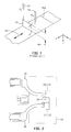
- FIG. 6 shows an illustrative embodiment, in perspective, of a typical slider 60 having read/write heads 40 formed on the slider trailing edge 62 .
- Slider 60 is suitable for use in a direct access storage device (DASD) using hard disk drives.
- Slider 60 has a rectangular rail 64 along each of the slider edges aligned parallel to the longitudinal axis of the slider.
- the top surface of each rail 64 forms the slider air bearing surface.
- the leading edge of each rail 64 has an upward-sloping ramp 66 formed across the entire width of rail 64 .
- Read/write head assembly 40 is mounted on or formed integrally with slider trailing edge 62 and has the read and write head elements exposed at air bearing surface 42 as detailed in FIGS. 3 and 4.
- FIG. 5 illustrates a single wafer substrate showing a plurality of interleaved read 20 and write head elements 70 fabricated thereon.
- the substrate wafer 68 is processed using thin film deposition technology to produce an array of read/write head elements 70 , each of which include at least one MR sensor element such as MR sensor element 26 shown in FIG. 2.
- QC quality control
- read/write head assemblies 70 shown on wafer substrate 68 in FIG. 5 it is possible to manually measure the read-width (RW) of a 25 few particular MR sensor element 26 (FIG. 2) by using electron microscopy.
- RW read-width
- FIG. 2 it is much more practical to automatically measure the electrical resistance of all MR element 26 by probing the appropriate pairs of sensor leads 36 (FIG. 2) using computer-controlled robotic equipment.
- the method of this invention uses both of these steps to screen every read/write head 70 on substrate 68 for acceptable read-width (RW) values.
- a heating-delta for MR sensor element 26 can be measured without referring to the actual element temperature, as may be understood with reference to the following discussion.
- the cold resistance RC is measured by applying a fixed bias current (for example, 1 mA) through the MR sensor element under test and (within a few milliseconds) measuring the voltage drop.
- the hot resistance RH is measured twice; once at constant-voltage for the RW determination and once again at constant-current for the SH determination.
- the constant-voltage measurement of RH is made by applying a fixed voltage (for instance, 200 mV) to the MR element under test and (within a few milliseconds) measuring the current.
- the inventors have found experimentally that, for a particular wafer substrate, the RW for any MR sensor element under test is related to the constant-voltage heating-delta for the same MR element.
- This experimental result is best appreciated with reference to FIG. 7, which provides the relationship between heating-delta 8 and read-width RW for seven different wafer substrates.
- the RW values are seen to vary from about 530 nm to 680 nm, which variation is seen to be related more or less predictably to the variation of heating-delta values from about 5.5% to 3.8%, respectively.
- a test coefficient CT k RW k 2 / ⁇ k is computed.
- the K values of CT k are then combined to produce a substrate coefficient CS representing the relationship shown in FIG. 7.
- the read-width RW can easily be estimated for every other MR sensor element from the constant-voltage RH and constant-current RC measurements needed to calculate the RW-related heating-deltas for each of the MR sensor elements.
- FIG. 8 illustrates the experimental results of tests made by the inventors to demonstrate the relationship between the heating-delta and bias current ratio (before and after heating) for a constant 200 mV bias voltage applied for 10 seconds.
- the clustering of experimental results in FIG. 8 demonstrates that there is a strong correlation between read-width RW and heating-delta ⁇ for any particular substrate wafer.
- FIG. 9 illustrates the experimental results of tests made by the inventors to demonstrate the relationship between the stripe height (SH) and constant-current heating-delta ⁇ for four different wafer substrates.
- the SH values are seen to vary from about 150 nm to 550 nm, which variation is seen to be related more or less predictably to the variation in bias current in arbitrary units.
- the precise relationship exemplified in FIG. 9 may be determined on a wafer-by-wafer basis by optically measuring the stripe-height SH of a few (for example, 200) MR sensor elements with an electron microscope and correlating the optical SH measurements with the automated constant-current heating-delta measurements for the same few MR sensor elements.
- the K values of CT k are then combined to produce a substrate coefficient CS representing the relationship shown in FIG. 7.
- FIG. 10 provides a block diagram showing an illustrative embodiment of the method of this invention for screening read-width values.
- a plurality, I of MR sensor elements are fabricated on a single wafer substrate (for example, wafer substrate 68 in FIG. 6).
- this plurality I may be 14,000 or so.
- a small sample of these MR sensor elements (a plurality, K) are selected for examination with an electron microscope.
- this plurality K may be 10 or so.
- the examination step 71 is performed, which provides a measured read-width value RW k for the k th MR sensor element.
- the substrate coefficient CS K is calculated.
- Substrate coefficient CS K represents an expected value computed from the small sample (K in number) of test coefficients CT k that were individually derived from the optically-measured read-widths RW k and automatically-measured deltas ⁇ k for the MR sensor element sample. For example, these measurements may be made on 200 such MR sensor elements on a single wafer substrate and an expected value for the substrate coefficient CS may be computed by using the mean value of the test coefficients.
- the inspection is performed by measuring the heating-delta ⁇ i for the i th MR sensor element and therefrom inferring the acceptance/rejection of the RW 1 for the i th MR sensor element. This measurement is accomplished in the step 78 of FIG. 10 for the i th MR sensor element.
- the measured heating-delta ⁇ i is tested ( ⁇ MIN ⁇ i ⁇ MAX ) against the acceptable range of values determined in step 76 above.
- the i th MR sensor element is rejected at the step 84 . Otherwise, the i th sensor element is accepted at the step 86 . Following the acceptance/rejection decisions, the index i is tested and incremented and the procedure repeated for the remaining MR sensor elements on the wafer substrate.
- a constant-voltage RH (hot resistance) is measured by applying a 200 mV voltage across the MR sensor element.
- the RC cold resistance is measured separately by passing a fixed current of 1 mA through the MR sensor element. Because the MR sensor element resistances are typically in the region of 40 ohms, the RH measurement is made at approximately 5 mA, which provides substantially more heating energy to the MR sensor element than does the 1 mA, thereby providing a “hot” resistance measurement.
- V bias voltage
- RW sensor read-width in metric units
- TCR temperature coefficient of resistance for substrate in (C.°) ⁇ 1 ,
- ⁇ 1 , ⁇ 2 thermal propagation coefficients of the surrounding substrate
- C T thermal conduction constant (not to be confused with test coefficient CT).
- the thermal propagation coefficients ⁇ 1 , ⁇ 2 are related directly to the length of the gap between upper or lower shield 34 , 38 and MR sensor 26 as seen in FIG. 3. Coefficients ⁇ 1 , ⁇ 2 are also related to the relative thermal conductivity between both shields 34 , 38 and the gap materials.
- Eqn. 3 demonstrates that, for the same substrate conditions and head geometry, the heating-delta can be used to compute the read-width by using the approximately-invariant substrate coefficient CS defined as follows: CS ⁇ V 2 ⁇ ⁇ TCR ⁇ ⁇ 1 ⁇ ⁇ 2 ( ⁇ 1 + ⁇ 2 ) ⁇ C T [ Eqn . ⁇ 4 ]
- a constant-current RH (hot resistance) is measured by applying a 4 mA current through the MR sensor element.
- the RC cold resistance is measured separately by passing a fixed current of 1 mA through the MR sensor element. The RH measurement is made with 16 times more heating energy to the MR sensor element than RC measurement, thereby providing a “hot” resistance measurement.
Landscapes
- Engineering & Computer Science (AREA)
- Manufacturing & Machinery (AREA)
- Magnetic Heads (AREA)
Abstract
An automated production process for the screening of the read-width (RW) and/or the stripe-height (SH) for every magnetoresistive (MR) read sensor element in a wafer substrate. The method of this invention uses the RW and/or SH values found with optical examination by electron microscopy of several of the MR sensor elements to estimate two substrate coefficients that relates the optical RW and SH measurements to heating-delta measurements, δ=(RH−RC)/RC, where RH is the sensor resistance when hot and RC is the sensor resistance when cold, both of which can be measured using automated equipment. These relationships are sufficiently similar among all MR sensor elements manufactured on a single wafer substrate during a single manufacturing procedure that, when the hot resistance RH is measured at a constant applied voltage, the heating-delta, may be used with a first substrate coefficient to estimate the read-width RW of each MR sensor element for quality-control purposes during manufacture. When the hot resistance RH is measured at a constant applied current, the heating-delta may be used with a second substrate coefficient to estimate the stripe-height SH of each MR sensor element for quality-control purposes during manufacture.
Description
- 1. Field of the Invention
- This invention relates generally to magnetoresistive (MR) read head sensing elements for magnetic data recording devices and, more particularly, to a rapid MR read head width measurement technique suitable for use during manufacture of data recording head assemblies.
- 2. Description of the Related Art
- Computer system secondary data storage is commonly provided in the form of a direct access storage device (DASD), such as a hard disk drive, a tape drive subsystem, or the like. A typical hard disk drive unit includes one or more rotating storage disks on which digital data is stored magnetically in a plurality of concentric tracks. Small read/write heads are positioned close to the rotating disk surface and moved from track to track to transfer data between the computer system and the spinning storage disk. Similarly, a typical tape drive unit includes a flexible magnetic tape on which data is stored magnetically in a plurality of parallel tracks. The tape is streamed over a small interleaved read/write head array to transfer data between the computer system and the tracks of the streaming tape. DASD read/write heads are usually manufactured by depositing various thin-films on a substrate to form an array of read head magneto-resistive (MR) sensor elements interleaved with write head magnetic gap elements. This substrate is then sliced and the pieces polished and mounted to produce read/write heads having the desired number of interleaved read and write elements for use in hard disk drives, tape drives, or the like.
- An MR head includes a center portion denominated the MR stripe, which is the element that senses changes in magnetic field representing data stored on a magnetic disk or tape surface in a DASD. MR read head sensors are well-known in the art and are particularly useful as read elements for high data recording densities. The MR read sensor provides a higher output signal than an inductive read head, which results in a higher signal-to-noise ratio for the playback channel, thereby permitting the reading of a higher areal density of recorded data on the magnetic disk surface. Such high data recording densities are possible because the MR sensor typically is very small (a 1 μm long stripe face with a read-width of 10 nm or less is typical). Because of the small sizes involved, modern MR read sensor fabrication is accomplished using monolithic thin film photolithographic fabrication technology. FIG. 5 illustrates a typical thin film wafer substrate on which an interleaved array of MR read sensor elements and magnetic gap elements have been fabricated. In the present art, 16,000 or more such interleaved read/write head pairs are fabricated on a single wafer substrate during one fabrication procedure.
- The sensitivity of an MR head depends on many factors. One of the most significant factors is the bias current provided to the MR head. The ability to read a signal from the storage media is, in part, a function of the amount of bias current supplied to the MR head. Signal sensitivity can be increased by increasing the amount of bias current supplied to the MR head. Therefore, increased bias current generally produces an improved signal-to-noise ratio and reduces bit error rates. However, simply increasing the bias current is not a complete solution because excessive current can significantly shorten the useful life span of the MR read head.
- Bias current can adversely affect MR read head life in two different ways. First, application of bias current in excessive quantities can cause the MR sensor element to overheat. If the current density reaches a high enough level, the MR element can burn out. This type of catastrophic failure is typically avoided by selecting a MR element bias current that avoids burnout over the entire operating temperature range.
- Catastrophic failure, however, is not the most common cause of MR read head failure. The most common cause of MR read head failure is a phenomenon known as electromigration and/or interlayer diffusion. Constant exposure to even normal operating levels of bias current will, over time, change the molecular structure of the MR sensor element, thereby degrading the magnetic sensing capability of the MR read head.
- During manufacture, the MR read heads are typically characterized to determine the range of their operating characteristics over temperature and bias current variations. The performance of MR heads fabricated on a given fabrication line may vary considerably because of process variations in the important geometric features on the heads, such as read-width (RW) and stripe height (SH). Proper Quality Control (QC) procedures must assure that even the MR read head with the worst-case geometric tolerances can provide a minimum desired lifetime. One option is for the designer to select a MR stripe bias current that holds the stripe temperature below a predetermined threshold, thereby providing the desired minimum lifetime for the DASD unit but at the expense of reducing MR sensor performance by producing all production heads for operation with the bias current selected for the worst-case element geometry.
- MR heads with sensor elements that fall within a nominal range of manufacturing tolerances may be driven with higher bias currents to boost their performance without exceeding the relevant temperature thresholds, but such higher bias current can shorten the life expectancy of the MR heads at the edge of expected manufacturing variations. Because an MR head should be operated below 155 degrees Celsius to avoid premature failure, the maximum bias current for all heads is typically set to equal the maximum bias current for the worst-case head.
- Because of the tradeoff between performance, bias current and element life expectancy, MR sensor element performance depends critically on the geometry of the MR stripe. Two important MR stripe dimensions are the read-width (RW) and the stripe height (SH), as they are known in the art. The MR read-width (RW) has an important effect on DASD performance because it directly affects the minimum available track width and, therefore, the maximum areal storage density for the DASD. Normally, in the art, the RW for a MR sensor can be measured only during production by using electron microscopy to visually inspect the physical MR element. Such a technique is unacceptably slow and burdensome for quality-control (QC) inspection in a MR element production line capable of fabricating 16,000 or more elements per wafer substrate. As a result of this problem, the usual production QC practice is to select a few exemplary MR elements from each wafer substrate for inspection by electron microscopy. This means that 99% or more of the MR read head elements are not properly inspected for acceptable RW value, requiring the bias current design compromises discussed above to accommodate expected geometric variations.
- There is accordingly a clearly-felt need in the art for a reasonably efficient technique for testing all MR sensor elements for proper stripe geometry during production. The related unresolved problems and deficiencies are clearly felt in the art and are solved by this invention in the manner described below.
- This invention solves the problem described above by providing for the first time a method for the automated production screening of the read-width (RW) and/or the stripe-height (SH) for every magnetoresistive (MR) read sensor element in a wafer substrate. The method of this invention uses the RW and/or SH values (optical SH measurements require the cross-sectioning of the sensor for measuring) found by optical examination with electron microscopy of several of the MR sensor elements to estimate two substrate coefficients that relates the optical RW and SH measurements to heating-delta measurements, δ=(RH−RC)/RC, where RH is the sensor resistance when hot and RC is the sensor resistance when cold, both of which can be measured using automated equipment These relationships are sufficiently similar among all MR sensor elements manufactured on a single wafer substrate during a single manufacturing procedure that, when the hot resistance RH is measured at a constant applied voltage, the heating-delta, may be used with a first substrate coefficient to estimate the read-width RW of each MR sensor element for quality-control purposes during manufacture. When the hot resistance RH is measured at a constant applied current, the heating-delta may be used with a second substrate coefficient to estimate the stripe-height SH of each MR sensor element for quality-control purposes during manufacture.
- It is a purpose of this invention to use such a substrate coefficient to estimate the read-width RW from a first heating-delta measured for any MR read sensor element on the same substrate. When the hot resistance RH is measured at a constant applied voltage, the resulting heating-delta, which can be measured using automated equipment, may be used with a first substrate coefficient to estimate the read-width RW of each MR sensor element for quality-control purposes during manufacture.
- It is an advantage of this invention that the read-width RW for every MR sensor element can be estimated from the optical measurement of RW for a few of the MR sensor elements and the automated measurement of a cold resistance and a constant-voltage hot resistance for all MR sensor elements on the substrate wafer.
- It is another purpose of this invention to use another substrate coefficient to estimate the throat height SH from a second heating-delta measured for any MR read sensor element on the same substrate. When the hot resistance RH is measured at a constant applied current, the resulting heating-delta, which can be measured using automated equipment, may be used to estimate the stripe-height SH of each MR sensor element for quality-control purposes during manufacture.
- It is another advantage of this invention that the throat height SH for every MR sensor elements can be estimated from the optical measurement of SH for a few of the MR sensor elements and the automated measurement of a cold resistance and a constant-current hot resistance for all MR sensor elements on the substrate wafer.
- In one embodiment, this invention is a method for determining the read-width RW i of one of a first plurality (I) of magnetoresistive (MR) sensor elements fabricated on a substrate, including the steps of optically measuring the read-width RWk of each of a second plurality (K<I) of the MR sensor elements, where i≠k=1, K, measuring a heating-delta δi for the one MR sensor element and a heating-delta δk for each of the second plurality (K<I) of MR sensor elements and calculating the read-width RWi of the one MR sensor element as a function of the optical read-width measurements RWk and the heating-delta measurements δi and δk.
- In another embodiment, this invention is a method for determining the stripe-height SH i of one of a first plurality (I) of magnetoresistive (MR) sensor elements fabricated on a substrate, including the steps of optically measuring the stripe-height SHk of each of a second plurality (K<I) of the MR sensor elements, where i≠k=1, K, measuring a heating-delta δi for the one MR sensor element and a heating-delta δk for each of the second plurality (K<I) of MR sensor elements, and calculating the stripe-height SHi of the one MR sensor element as a function of the optical stripe-height measurements SHk and the heating-delta measurements δi and δk.
- In yet another embodiment, this invention is a process for manufacturing magnetoresistive (MR) heads having a read-width RW j within a predetermined range (RWmax, RWmin) including the steps of fabricating a first plurality (I) of magnetoresistive (MR) sensor elements on a substrate, optically measuring the read-width RWk of each of a second plurality (K<I) of the MR sensor elements, where k=1, K, measuring a heating-delta δi for each of the first plurality (I) of MR sensor elements, calculating an upper heating-delta limit δmax and a lower heating-delta limit δi, for the MR sensor elements as a function of the optical read-width measurements RWk and the heating-delta measurements δk, and selecting those MR sensor elements for which the heating-delta δj is within the range (δmax,δmin) for use in making the magnetoresistive (MR) heads.
- In still another embodiment, this invention is a process for manufacturing magnetoresistive (MR) heads having a stripe-height SH j within a predetermined range (SHmax, SHmin) including the steps of fabricating a first plurality (I) of magnetoresistive (MR) sensor elements on a substrate, optically measuring the stripe-height SHk of each of a second plurality (K<I) of the MR sensor elements, where k=1, K, measuring a heating-delta δi for each of the first plurality (I) of MR sensor elements, calculating an upper heating-delta limit δmax and a lower heating-delta limit δmin for the MR sensor elements as a function of the optical stripe-height measurements SHk and the heating-delta measurements δk, and selecting those MR sensor elements for which the heating-delta δj is within the range (δmax,δmin) for use in making the magnetoresistive (MR) heads.
- In another embodiment, this invention is a process for manufacturing read/write heads for direct access storage devices (DASDs) including magnetic gap write elements interleaved with magnetoresistive (MR) sensor read elements each having a read-width RW j within a first predetermined range (RWmax, RWmin) and a stripe-height SHj within a second predetermined range (SHmax, SHmin) including the steps of fabricating a first plurality (I) of MR sensor elements on a substrate optically measuring the read-width RWk of each of a second plurality (K<I) of the MR sensor elements, where k=1, K, measuring a first heating-delta δi for each of the first plurality (I) of MR sensor elements, calculating a first upper heating-delta limit δmax and a first lower heating-delta limit δmin for the MR sensor elements as a function of the optical read-width measurements RWk and the first heating-delta measurements δk, measuring the stripe-height SHk of each of a second plurality (K<I) of the MR sensor elements, where k=1, K, measuring a second heating-delta δi for each of the first plurality (I) of MR sensor elements, calculating a second upper heating-delta limit δmax and a second lower heating-delta limit δmin for the MR elements as a function of the optical stripe-height measurements SHk and the second heating-delta measurements δk, and selecting those MR sensor elements for which the first heating-delta δj is within the first range (δmax, δmin) and the second heating-delta δj is within the second range (δmax, δmin) for use in making the read/write heads.
- The foregoing, together with other objects, features and advantages of this invention, can be better appreciated with reference to the following specification, claims and the accompanying drawing.
- For a more complete understanding of this invention, reference is now made to the following detailed description of the embodiments as illustrated in the accompanying drawing, in which like reference designations represent like features throughout the several views and wherein:
- FIG. 1 shows a schematic diagram illustrating the various dimensions and features of the MR stripe used as a read head sensor;
- FIG. 2 illustrates a plan view of a typical MR read sensor element known in the art;
- FIG. 3 illustrates the MR read sensor element of FIG. 2 viewed from the side;
- FIG. 4 illustrates the MR read sensor element of FIG. 2 viewed from the front air bearing surface (ABS);
- FIG. 5 illustrates a single wafer substrate showing a plurality of interleaved read/write head elements fabricated thereon;
- FIG. 6 shows an illustrative embodiment of a read/write head and slider assembly suitable for use in a hard disk drive;
- FIG. 7 shows an experimentally-measured 1 relationship between read-width (RW) and heating-delta for MR read sensor elements as determined for the first time by the inventors;
- FIG. 8 shows an experimentally-measured relationship between heating-delta and a time rate of change of voltage-drop at fixed current for MR read sensor elements as determined for the first time by the inventors;
- FIG. 9 shows an experimentally-measured relationship between stripe height (SH) and bias current for MR read sensor elements as determined by the inventors; and
- FIGS. 10A and 10B illustrate a flow chart diagram of the method of this invention.
- FIG. 1 shows a magnetoresistive (MR) read sensor strip geometry known in the art. In its simplest form, the MR sensor element consists of a
narrow stripe 20 of magnetoresistive materials such as NiFe, NiCo or CoFe, of height SH and width RW. Thestripe 20 is mounted in a plane perpendicular to therecording medium 22 and connected to theconductors 24 at each end carrying a sense current Is. Because of the magnetoresistive effect, the resistivity of each portion ofstripe 20 depends on the angle θ between the direction of magnetization Ns and the current density vector, as is well-known in the art. In a spin valve sensor, the resistivity varies as a function of the angle between the magnetic moments of the free and pinned layers. - Thin film techniques are widely used for fabricating MR sensor elements because of the advantageous effects of very narrow read-with (RW) and stripe height (SH). FIG. 2 shows a top plan view of a
MR sensor element 26.MR sensor 26 includes thestripe 20. Referring to FIG. 4, the conductor and hard bias layers 28 and 30 and the conductor and hard bias layers 31 and 32 are coupled toMR sensor element 26 in a spatial relationship that defines the read-width RW. Hard bias layers 30 and 32 are included to stabilize the magnetic domains ofMR sensor element 26 in the well-known manner. The read/write head 40 also includes anupper MR shield 34 and a lower MR shield 38 (shown in FIG. 3; onlyMR shield 34 is shown in FIG. 2 becauselower MR shield 38 is directly below). The sensor leads 36 are thin gold conductors for conducting bias current throughMR sensor element 26 via conductor layers 28 and 31 and hard bias layers 30 and 32. - FIG. 3 shows a read/
write head assembly 40 viewed from the side. Read/write head 40 includesMR sensor element 26 discussed above in connection with FIG. 2 and a separateinductive write assembly 43 formed adjacent one another on a substrate 44 A portion of the read/write head 40 is shown in transducing relationship with the movingmagnetic recording medium 22. The head air bearing surface (ABS) 42 is disposed in facing relationship with and slightly above the recording surface ofrecording medium 22. Typically, read/write head 40 (FIG. 3) represents a single pair of read and write elements (MR sensor element 26 and inductive write assembly 43).MR sensor element 26 is enclosed byupper MR shield 34 andlower MR shield 38. Sensor leads 36 (shown in FIG. 2) coupleMR sensor element 26 to external circuitry (not shown) to provide for sensing the resistance ofMR sensor element 26 as changed by external magnetic fields. - The MR read assembly is formed by vacuum deposition techniques, such as sputter deposition, for example, on the
substrate 44. The various elements of the MR assembly discussed above are surrounded and insulated from one another with layers, exemplified by thelayer 46, of insulating material, such as silicon dioxide or aluminum oxide, for example. - The inductive write assembly includes a lower or
first pole piece 48 and an upper orsecond pole piece 50.Pole pieces second pole tips magnetic gap 56 at theair bearing surface 42, thereby acting as a magnetic gap write element. One or more write coils are disposed between first andsecond pole pieces coil 58 is also connected to external circuitry (not shown) via conductive leads (not shown).Pole pieces coil 58 are usually fabricated by well-known processes such as electroplating or sputter deposition, for example.Pole pieces write coil 58 and the MR read assembly by layers, exemplified bylayer 46, of insulating and protective material. Read/write head 40 is sometimes denominated a “piggyback” head assembly. In an alternative embodiment, sometimes denominated a “merged” head assembly,first pole piece 48 also serves as a second shield layer for the read assembly, in whichcase layer 34 is omitted. Either configuration can be repeated to define a “interleaved” read/write head consisting of alternating read and write elements substantially as shown. - FIG. 4 illustrates the typical read/
write head assembly 40 from FIG. 3 viewed from the front air bearing surface 42 (FIG. 3). FIG. 4 may be appreciated with reference to the above description of read/write head assembly 40 shown in FIG. 3. Note that the read-width (RW) ofMR sensor element 26 is roughly equivalent to the height ofsecond pole tip 54, which together govern the requisite track width for the recording medium. - FIG. 6 shows an illustrative embodiment, in perspective, of a
typical slider 60 having read/write heads 40 formed on theslider trailing edge 62.Slider 60 is suitable for use in a direct access storage device (DASD) using hard disk drives.Slider 60 has arectangular rail 64 along each of the slider edges aligned parallel to the longitudinal axis of the slider. The top surface of eachrail 64 forms the slider air bearing surface. The leading edge of eachrail 64 has an upward-slopingramp 66 formed across the entire width ofrail 64. Read/write head assembly 40 is mounted on or formed integrally withslider trailing edge 62 and has the read and write head elements exposed atair bearing surface 42 as detailed in FIGS. 3 and 4. - FIG. 5 illustrates a single wafer substrate showing a plurality of interleaved read 20 and write
head elements 70 fabricated thereon. Thesubstrate wafer 68 is processed using thin film deposition technology to produce an array of read/write head elements 70, each of which include at least one MR sensor element such asMR sensor element 26 shown in FIG. 2. During quality control (QC) testing of read/write head assemblies 70 shown onwafer substrate 68 in FIG. 5, it is possible to manually measure the read-width (RW) of a 25 few particular MR sensor element 26 (FIG. 2) by using electron microscopy. However, it is much more practical to automatically measure the electrical resistance of allMR element 26 by probing the appropriate pairs of sensor leads 36 (FIG. 2) using computer-controlled robotic equipment. The method of this invention, as discussed below in connection with FIG. 10, uses both of these steps to screen every read/write head 70 onsubstrate 68 for acceptable read-width (RW) values. - The method of this invention arises from the unexpectedly advantageous observation that the read-width RW and the stripe-height SH for
MR sensor element 26 are each related by one of two substrate coefficients to a heating-delta, δ=(RH−RC)/RC, forMR sensor element 26. A heating-delta forMR sensor element 26 can be measured without referring to the actual element temperature, as may be understood with reference to the following discussion. - For purposes of the method of this invention, a three-step process for measuring both heating deltas is preferred. The cold resistance RC is measured by applying a fixed bias current (for example, 1 mA) through the MR sensor element under test and (within a few milliseconds) measuring the voltage drop. The hot resistance RH is measured twice; once at constant-voltage for the RW determination and once again at constant-current for the SH determination. The constant-voltage measurement of RH is made by applying a fixed voltage (for instance, 200 mV) to the MR element under test and (within a few milliseconds) measuring the current. The constant-current measurement of RH is made by applying a fixed current (for instance, 4 mA) to the MR element under test and (within a few milliseconds) measuring the current. For each of the two RH measurements, the heating-delta δ=(RH−RC)/RC may be readily and automatically computed. If the read-width RW alone is to be tested, the second constant-current RH measurement may be omitted.
- The inventors have found experimentally that, for a particular wafer substrate, the RW for any MR sensor element under test is related to the constant-voltage heating-delta for the same MR element. This experimental result is best appreciated with reference to FIG. 7, which provides the relationship between heating-delta 8 and read-width RW for seven different wafer substrates. The RW values are seen to vary from about 530 nm to 680 nm, which variation is seen to be related more or less predictably to the variation of heating-delta values from about 5.5% to 3.8%, respectively. The precise relationship exemplified in FIG. 7 may be determined on a wafer-by-wafer basis by optically measuring the read-width RW of a few (for example, 200) MR sensor elements with an electron microscope and correlating the optical RW measurements with the automated constant-voltage heating-delta measurements for the same few MR sensor elements. For each of these measurements (k=1, K where K is about 200), a test coefficient CTk RWk 2/δk is computed. The K values of CTk are then combined to produce a substrate coefficient CS representing the relationship shown in FIG. 7. Once the substrate coefficient (CS=RW2/δ) is established by combining the optical RW measurements for the MR sensor element sample, then the read-width RW can easily be estimated for every other MR sensor element from the constant-voltage RH and constant-current RC measurements needed to calculate the RW-related heating-deltas for each of the MR sensor elements.
- FIG. 8 illustrates the experimental results of tests made by the inventors to demonstrate the relationship between the heating-delta and bias current ratio (before and after heating) for a constant 200 mV bias voltage applied for 10 seconds. The clustering of experimental results in FIG. 8 demonstrates that there is a strong correlation between read-width RW and heating-delta δ for any particular substrate wafer.
- FIG. 9 illustrates the experimental results of tests made by the inventors to demonstrate the relationship between the stripe height (SH) and constant-current heating-delta δ for four different wafer substrates. The SH values are seen to vary from about 150 nm to 550 nm, which variation is seen to be related more or less predictably to the variation in bias current in arbitrary units. The precise relationship exemplified in FIG. 9 may be determined on a wafer-by-wafer basis by optically measuring the stripe-height SH of a few (for example, 200) MR sensor elements with an electron microscope and correlating the optical SH measurements with the automated constant-current heating-delta measurements for the same few MR sensor elements. For each of these measurements (k=1, K where K is about 200), a test coefficient CT k=RWk 2/δ k is computed. The K values of CTk are then combined to produce a substrate coefficient CS representing the relationship shown in FIG. 7. Once the substrate coefficient (CS =RW2/δ) is established by combining the optical SH measurements for the MR sensor element sample, then the stripe-height SH can easily be estimated for every other MR sensor element from the constant-current RH and RC measurements needed to calculate the SH-related heating-deltas for each of the MR sensor elements.
- FIG. 10 provides a block diagram showing an illustrative embodiment of the method of this invention for screening read-width values. For the purpose of appreciating FIG. 10, it is assumed that a plurality, I, of MR sensor elements are fabricated on a single wafer substrate (for example,
wafer substrate 68 in FIG. 6). For example, this plurality I may be 14,000 or so. In the method of this invention, a small sample of these MR sensor elements (a plurality, K) are selected for examination with an electron microscope. For example, this plurality K may be 10 or so. For each of the K sensor elements, theexamination step 71 is performed, which provides a measured read-width value RWk for the kth MR sensor element.Step 71 is repeated for every integer k=1, K as may be understood with reference to FIG. 10. After completingstep 71 for the Kth MR sensor element, the process then proceeds to thestep 72 where the index k is reset to unity and, in thestep 74, the heating-delta δ=( RH−Rc)/Rc is computed for each of the MR sensor elements in a loop for every integer k=1, K. Afterstep 74 is completed for the Kth sensor element, the substrate coefficient CSK is calculated. Substrate coefficient CSK represents an expected value computed from the small sample (K in number) of test coefficients CTk that were individually derived from the optically-measured read-widths RWk and automatically-measured deltas δk for the MR sensor element sample. For example, these measurements may be made on 200 such MR sensor elements on a single wafer substrate and an expected value for the substrate coefficient CS may be computed by using the mean value of the test coefficients. - Using the substrate coefficient expected value, CS K, an acceptable range of heating-deltas from δmax=CSK/(RWmin)2 to δ min=CSK/(RWmax)2 is computed in the
step 76. It may be readily appreciated that the heating-delta range computed instep 76 is a result of the measurements of the K sensor element sample alone. The reasoning behind the form of the computation is discussed below. After completingstep 76, each of the plurality I MR sensor elements in the substrate wafer are inspected for acceptance or rejection. Although the acceptance criterion for the ith MR sensor element is the read-width, (RWmin <RWi<RWmax), the inspection is performed by measuring the heating-delta δifor the ith MR sensor element and therefrom inferring the acceptance/rejection of the RW1 for the ith MR sensor element. This measurement is accomplished in thestep 78 of FIG. 10 for the ith MR sensor element. At thesteps step 76 above. If the measured heating-delta δi falls outside the acceptable heating-delta range (δMIN, δMAX), then the ith MR sensor element is rejected at thestep 84. Otherwise, the ith sensor element is accepted at thestep 86. Following the acceptance/rejection decisions, the index i is tested and incremented and the procedure repeated for the remaining MR sensor elements on the wafer substrate. - As discussed above in connection with FIGS. 7-9, the inventors have determined through experimental measurement that the method of this invention provides a reliable QC screening technique for MR head elements of the type discussed hereinabove. The inventors also have developed a theoretical explanation for the usefulness of the relationship between read-width RW, stripe-height SH and the two heating-deltas δ. Eqn. 1 describes the definition of the heating-delta in terms of resistance values measured at two different temperatures RH and RC:
- δ=(RH−RC)/RC [Eqn. 1]
- For read-width RW determination, a constant-voltage RH (hot resistance) is measured by applying a 200 mV voltage across the MR sensor element. The RC (cold resistance) is measured separately by passing a fixed current of 1 mA through the MR sensor element. Because the MR sensor element resistances are typically in the region of 40 ohms, the RH measurement is made at approximately 5 mA, which provides substantially more heating energy to the MR sensor element than does the 1 mA, thereby providing a “hot” resistance measurement.
- Considering that the heating of the MR sensor element, ΔT, is equal to the heating power multiplied by the thermal impedance, it follows that:

- where: δ=heating delta from Eqn. 1,
- V=bias voltage,
- p=substrate sheet resistivity in ohms/square,
- RW=sensor read-width in metric units,
- TCR=temperature coefficient of resistance for substrate in (C.°) −1,
- τ 1, τ2 =thermal propagation coefficients of the surrounding substrate, and
- C T=thermal conduction constant (not to be confused with test coefficient CT).
- The thermal propagation coefficients τ 1, τ2 are related directly to the length of the gap between upper or
lower shield MR sensor 26 as seen in FIG. 3. Coefficients τ1, τ2 are also related to the relative thermal conductivity between bothshields - Considering that τ<<1 (for example, 3%), then the approximation can be made as shown in Eqn. 3:
- δ(1+δ)≈δ [Eqn. 3]
- Eqn. 3 demonstrates that, for the same substrate conditions and head geometry, the heating-delta can be used to compute the read-width by using the approximately-invariant substrate coefficient CS defined as follows:

- Note that the right-hand side of Eqn. 4 is constant (for the same substrate) if the bias voltage V is constant. For this reason, the constant-voltage RH measurement is used to derive the heating delta δ(per Eqn. 1 ) used to determine read-width RW from the substrate coefficient CS of Eqn. 4.
- For stripe-height SH determination, a constant-current RH (hot resistance) is measured by applying a 4 mA current through the MR sensor element. As was done for read-width RW determination, the RC (cold resistance) is measured separately by passing a fixed current of 1 mA through the MR sensor element. The RH measurement is made with 16 times more heating energy to the MR sensor element than RC measurement, thereby providing a “hot” resistance measurement.
- The inventors have shown that the heating-delta is related to the stripe height SH according to the Eqn. 5 :

- Again, because δ<<1, Eqn. 5 can be approximated by following equation:

- where

- Note that the right-hand side of Eqn. 7 is constant (for the same substrate) if the bias current I is constant. For this reason, the constant-current RH measurement is used to derive the heating delta δ(per Eqn. 1) used to determine stripe-height SH from the substrate coefficient CS of Eqn. 6.
- Clearly, other embodiments and modifications of this invention may occur readily to those of ordinary skill in the art in view of these teachings. Therefore, this invention is to be limited only by the following claims, which include all such embodiments and modifications when viewed in conjunction with the above specification and accompanying drawing.
Claims (24)
1. A method for determining the read-width RWi of one of a first plurality (I) of magnetoresistive (MR) sensor elements fabricated on a substrate, the method comprising the steps of:
optically measuring the read-width RWk of each of a second plurality (K<I) of the MR sensor elements, where i≠k=1, K;
measuring a heating-delta δi for the one MR sensor element and a heating-delta δk for each of the second plurality (K<I) of MR sensor elements; and
calculating the read-width RWi of the one MR sensor element as a function of the optical read-width measurements RWk and the heating-delta measurements δi and δk.
2. The method of claim 2 further comprising the step of:
calculating an expected value of a substrate coefficient CSK as a function of the optical read-width measurements RWk and the heating-delta measurements δk.
3. The method of claim 3 further comprising the steps of:
calculating a test coefficient CTk=(RWk)2/δ k for each of the second plurality (K<I) of MR sensor elements; and
combining the second plurality of test coefficients CTk to obtain the expected value of the substrate coefficient CSK.
4. The method of claim 3 further comprising the steps of:
measuring a cold resistance RCi when a fixed current is applied to the ith MR sensor element;
measuring a hot resistance RHi when a fixed voltage is applied to the ith MR sensor element; and
computing the heating-delta δi=(RHi −RCi )/RCi for the ith MR sensor element.
5. The method of claim 4 further comprising the step of:
calculating the read-width RWi=(δi·CSK) 1/2 for the one MR sensor element.
6. A method for determining the stripe-height SHi of one of a first plurality (I) of magnetoresistive (MR) sensor elements fabricated on a substrate, the method comprising the steps of:
optically measuring the stripe-height SHk of each of a second plurality (K<I) of the MR sensor elements, where i≠k=1, K;
measuring a heating-delta δi for the one MR sensor element and a heating-delta δk for each of the second plurality (K<I) of MR sensor elements; and
calculating the stripe-height SHi of the one MR sensor element as a function of the optical stripe-height measurements SHk and the heating-delta measurements δi and
7. The method of claim 6 further comprising the step of:
calculating an expected value of a substrate coefficient CSK as a function of the optical stripe-height measurements SHk and the heating-delta measurements δk .
8. The method of claim 7 further comprising the steps of:
measuring a cold resistance RCi when a first fixed current is applied to the ith MR sensor element;
measuring a hot resistance RHi when a second fixed current is applied to the ith MR sensor element; and
computing the heating-delta δi=(RHi−RC1 ,)/RCi for the ith MR sensor element.
9. A process for manufacturing magnetoresistive (MR) heads having a read-width RWj within a predetermined range (RWmax, RWmin) comprising the steps of:
fabricating a first plurality (I) of magnetoresistive (MR) sensor elements on a substrate;
optically measuring the read-width RWk of each of a second plurality (K<I) of the MR sensor elements, where k=1, K;
measuring a heating-delta δi for each of the first plurality (I) of MR sensor elements;
calculating an upper heating-delta limit δmax and a lower heating-delta limit δmin for the MR sensor elements as a function of the optical read-width measurements RWk and the heating-delta measurements δk; and
selecting those MR sensor elements for which the heating-delta δj is within the range (δmax, δmin) for use in making the magnetoresistive (MR) heads.
10. The process of claim 9 further comprising the step of:
calculating an expected value of a substrate coefficient CSK as a function of the optical read-width measurements RWk and the heating-delta measurements δk.
11. The process of claim 10 further comprising the steps of:
calculating a test coefficient CTk=(RWk)2/δ k for each of the second plurality (K<I) of MR sensor elements; and
combining the second plurality of test coefficients CTk to obtain the expected value of the substrate coefficient CSK.
12. The process of claim 11 further comprising the steps of:
measuring a cold resistance RCi when a fixed current is applied to the ith MR sensor element;
measuring a hot resistance RHi when a fixed voltage is applied to the ith MR sensor element; and
computing the heating-delta δ=(RHi−RCi)/RCi for the ithMR sensor element.
13. The process of claim 12 further comprising the step of:
calculating the read-width RWi=(δi·CSK)1/2 for each of the first plurality (I) of MR sensor elements.
14. A process for manufacturing magnetoresistive (MR) heads having a stripe-height SHj within a predetermined range (SHmax, SHmin) comprising the steps of:
fabricating a first plurality (I) of magnetoresistive (MR) sensor elements on a substrate;
optically measuring the stripe-height SHk of each of a second plurality (K<I) of the MR sensor elements, where k=1, K;
measuring a heating-delta δi for each of the first plurality (I) of MR sensor elements;
calculating an upper heating-delta limit δmax and a lower heating-delta limit δmin for the MR sensor elements as a function of the optical stripe-height measurements SHk and the heating-delta measurements δk; and
selecting those MR sensor elements for which the heating-delta δj is within the range (δmax, δmin,) for use in making the magnetoresistive (MR) heads.
15. The process of claim 14 further comprising the step of:
calculating an expected value of a substrate coefficient CSK as a function of the optical stripe-height measurements SHk and the heating-delta measurements δk
16. The process of claim 15 further comprising the steps of:
calculating a test coefficient CTk=(RWk)2/δk for each of the second plurality (K<I) of MR sensor elements; and
combining the second plurality of test coefficients CTk to obtain the expected value of the substrate coefficient CSK.
17. The process of claim 16 further comprising the steps of:
measuring a cold resistance RCi when a first fixed current is applied to the ith MR sensor element;
measuring a hot resistance RHi when a second fixed current is applied to the ith MR sensor element; and
computing the heating-delta δi=(RHi−RCi)/RCi for the ith MR sensor element.
18. The process of claim 17 further comprising the step of:
calculating the stripe-height SHi=(δi·CSK)1/2 for each of the first plurality (I) of MR sensor elements.
19. A process for manufacturing read/write heads for direct access storage devices (DASDs) including magnetic gap write elements interleaved with magnetoresistive (MR) sensor read elements each having a read-width RWj within a first predetermined range (RWmax, RWmin) and a stripe-height SHj within a second predetermined range (SHmax, SHmin), the method comprising the steps of:
fabricating a first plurality (I) of MR sensor elements on a substrate;
optically measuring the read-width RWk of each of a second plurality (K<I) of the MR sensor elements, where k=1, K;
measuring a first heating-delta δi for each of the first plurality (I) of MR sensor elements;
calculating a first upper heating-delta limit δmax and a first lower heating-delta limit δmin for the MR sensor elements as a function of the optical read-width measurements RWk and the first heating-delta measurements δk; and
selecting those MR sensor elements for which the first heating-delta δj is within the first range (δmax, δmin) for use in making the read/write heads.
20. The process of claim 19 further comprising the step of:
calculating an expected value of a first substrate coefficient CSK as a function of the optical read-width measurements RWk and the first heating-delta measurements δk.
21. The process of claim 19 further comprising the steps of:
measuring a cold resistance RCi when a fixed current is applied to the ith MR sensor element;
measuring a hot resistance RHi when a fixed voltage is applied to the ith MR sensor element; and
computing the first heating-delta δi=(RHi−RCi)/RCi for the ith MR sensor element.
22. The process of claim 19 further comprising the steps of:
measuring the stripe-height SHk of each of a second plurality (K<I) of the MR sensor elements, where k=1, K;
measuring a second heating-delta δi for each of the first plurality (I) of MR sensor elements;
calculating a second upper heating-delta limit δmax and a second lower heating-delta limit δmin for the MR elements as a function of the optical stripe-height measurements SHk and the second heating-delta measurements δk ; and
selecting those MR sensor elements for which the second heating-delta δj is within the second range (δmax, δmin) for use in making the read/write heads.
23. The process of claim 22 further comprising the step of:
calculating an expected value of a second substrate coefficient CSK as a function of the optical stripe-height measurements SHk and the second heating-delta measurements δk.
24. The process of claim 23 further comprising the steps of:
measuring a second hot resistance RH2i when a second fixed current is applied to the ith MR sensor element; and
computing the second heating-delta δi=(RH2i−RCi)/RCi for the ith MR sensor element.
Priority Applications (1)
| Application Number | Priority Date | Filing Date | Title |
|---|---|---|---|
| US10/125,212 US6762914B2 (en) | 2002-04-17 | 2002-04-17 | Method for the rapid measurement of magnetoresistive read head dimensions |
Applications Claiming Priority (1)
| Application Number | Priority Date | Filing Date | Title |
|---|---|---|---|
| US10/125,212 US6762914B2 (en) | 2002-04-17 | 2002-04-17 | Method for the rapid measurement of magnetoresistive read head dimensions |
Publications (2)
| Publication Number | Publication Date |
|---|---|
| US20030197854A1 true US20030197854A1 (en) | 2003-10-23 |
| US6762914B2 US6762914B2 (en) | 2004-07-13 |
Family
ID=29214753
Family Applications (1)
| Application Number | Title | Priority Date | Filing Date |
|---|---|---|---|
| US10/125,212 Expired - Fee Related US6762914B2 (en) | 2002-04-17 | 2002-04-17 | Method for the rapid measurement of magnetoresistive read head dimensions |
Country Status (1)
| Country | Link |
|---|---|
| US (1) | US6762914B2 (en) |
Cited By (1)
| Publication number | Priority date | Publication date | Assignee | Title |
|---|---|---|---|---|
| US9387568B1 (en) * | 2013-02-27 | 2016-07-12 | Western Digital Technologies, Inc. | Systems and methods for correcting fabrication error in magnetic recording heads using magnetic write width measurements |
Families Citing this family (6)
| Publication number | Priority date | Publication date | Assignee | Title |
|---|---|---|---|---|
| JP2003203312A (en) * | 2002-01-10 | 2003-07-18 | Fujitsu Ltd | Magneto-resistance effect head and information reproducing device |
| US7564235B2 (en) * | 2006-08-11 | 2009-07-21 | Hitachi Global Storage Technologies Netherlands B.V. | Determination of magnetic read head properties |
| US8044816B2 (en) * | 2007-02-01 | 2011-10-25 | International Business Machines Corporation | Apparatus, system, and method for detecting the formation of a short between a magnetoresistive head and a head substrate |
| US7804657B1 (en) | 2007-06-11 | 2010-09-28 | Western Digital Technologies, Inc. | Setting an operating bias current for a magnetoresistive head using ratio of target voltage and measured voltage |
| US7872824B1 (en) | 2007-06-11 | 2011-01-18 | Western Digital (Fremont), Llc | Setting an operating bias current for a magnetoresistive head by computing a target operating voltage |
| US7760458B1 (en) | 2008-08-12 | 2010-07-20 | Western Digital Technologies, Inc. | Disk drive adjusting head bias during servo synchronization to compensate for over/under sensitivity |
Citations (3)
| Publication number | Priority date | Publication date | Assignee | Title |
|---|---|---|---|---|
| US6515475B2 (en) * | 2001-02-16 | 2003-02-04 | International Business Machines Corporation | Determination of track width of magnetoresistive sensors during magnetic head fabrication using magnetic fields |
| US6581271B2 (en) * | 1998-05-06 | 2003-06-24 | Tdk Corporation | Method of manufacturing thin-film magnetic head |
| US6642713B2 (en) * | 2001-03-28 | 2003-11-04 | International Business Machines Corporation | Absolute track width measurement on magnetic recording heads |
Family Cites Families (2)
| Publication number | Priority date | Publication date | Assignee | Title |
|---|---|---|---|---|
| US5790334A (en) | 1996-10-02 | 1998-08-04 | International Business Machines Corporation | Circuit and method for optimizing bias supply in a magnetoresistive head based on the thermal properties of the MR head itself |
| JP2001006129A (en) * | 1999-06-22 | 2001-01-12 | Sony Corp | Lapping guide for MR element and stripe height measuring method |
-
2002
- 2002-04-17 US US10/125,212 patent/US6762914B2/en not_active Expired - Fee Related
Patent Citations (3)
| Publication number | Priority date | Publication date | Assignee | Title |
|---|---|---|---|---|
| US6581271B2 (en) * | 1998-05-06 | 2003-06-24 | Tdk Corporation | Method of manufacturing thin-film magnetic head |
| US6515475B2 (en) * | 2001-02-16 | 2003-02-04 | International Business Machines Corporation | Determination of track width of magnetoresistive sensors during magnetic head fabrication using magnetic fields |
| US6642713B2 (en) * | 2001-03-28 | 2003-11-04 | International Business Machines Corporation | Absolute track width measurement on magnetic recording heads |
Cited By (1)
| Publication number | Priority date | Publication date | Assignee | Title |
|---|---|---|---|---|
| US9387568B1 (en) * | 2013-02-27 | 2016-07-12 | Western Digital Technologies, Inc. | Systems and methods for correcting fabrication error in magnetic recording heads using magnetic write width measurements |
Also Published As
| Publication number | Publication date |
|---|---|
| US6762914B2 (en) | 2004-07-13 |
Similar Documents
| Publication | Publication Date | Title |
|---|---|---|
| US7872471B2 (en) | Testing method of head element and magnetic recording and reproducing apparatus capable of head evaluating | |
| US8351162B2 (en) | Magnetic head with electro lapping guide | |
| US7583479B2 (en) | Thin-film magnetic head with heater in overcoat multilayer, head gimbal assembly with thin-film magnetic head, and magnetic disk drive apparatus with head gimbal assembly | |
| US7961429B2 (en) | Thin-film magnetic head having heating element with lower-resistance portion | |
| JP4021369B2 (en) | Thin film magnetic head, temperature monitoring and feedback system, and tape head | |
| US7649713B2 (en) | Thin-film magnetic head with heating element and heatsink | |
| US7986481B2 (en) | Magnetic reproducing method for suppressing low temperature noise | |
| US8085038B2 (en) | Method for testing noise of thin-film magnetic head, and magnetic disk drive apparatus with noise testing function | |
| US20080102316A1 (en) | Magneto-resistive magnetic read head and storage apparatus using the same magnetic read head | |
| US7813085B2 (en) | Thin-film magnetic head having laminate shields for tolerating external magnetic field | |
| US6731110B2 (en) | Magneto-resistive device with built-in test structure and method for determining resistance and track width | |
| US6762914B2 (en) | Method for the rapid measurement of magnetoresistive read head dimensions | |
| US6678127B2 (en) | Device and method of reducing ESD damage in thin film read heads which enables measurement of gap resistances and method of making | |
| JP3421983B2 (en) | Method of manufacturing composite thin film magnetic head | |
| US7916434B2 (en) | Tunnel magnetoresistive effect element with limited electric popping output voltage | |
| US11823712B2 (en) | Built-in resistance sensor for measuring slider level pole width at point “A” (PWA) for PMR/MAMR writers | |
| US7643247B2 (en) | β-phase tantalum thin-film resistor and thin-film magnetic head with the resistor | |
| JP2001006128A (en) | Manufacture of magnetic converting element and its device and manufacture of magnetic head and its device | |
| JP4179260B2 (en) | Magnetoresistive magnetic head and magnetic tape device | |
| US6404603B1 (en) | Thin film device, thin film head, and magnetoresistive element | |
| Ju et al. | A combined experimental and numerical study of temperature rise in GMR sensors due to self-heating | |
| US7009818B1 (en) | Thin film magnetic head having improved thermal characteristics, and method of manufacturing | |
| US6633459B2 (en) | Functional recording-head on-slider lap monitor | |
| Imamura et al. | An FEM analysis of the temperature rise distribution in a GMR head due to the sense current and contact resistance | |
| JP2008171530A (en) | Magnetoresistive element manufacturing method and inspection method |
Legal Events
| Date | Code | Title | Description |
|---|---|---|---|
| AS | Assignment |
Owner name: INTERNATIONAL BUSINESS MACHINES CORPORATION, NEW Y Free format text: ASSIGNMENT OF ASSIGNORS INTEREST;ASSIGNORS:FOX, CIARAN A.;MELZ, PETER JOHN;LUO, JIH-SHIUAN;AND OTHERS;REEL/FRAME:012843/0653;SIGNING DATES FROM 20001221 TO 20020415 |
|
| FEPP | Fee payment procedure |
Free format text: PAYOR NUMBER ASSIGNED (ORIGINAL EVENT CODE: ASPN); ENTITY STATUS OF PATENT OWNER: LARGE ENTITY |
|
| REMI | Maintenance fee reminder mailed | ||
| LAPS | Lapse for failure to pay maintenance fees | ||
| STCH | Information on status: patent discontinuation |
Free format text: PATENT EXPIRED DUE TO NONPAYMENT OF MAINTENANCE FEES UNDER 37 CFR 1.362 |
|
| FP | Lapsed due to failure to pay maintenance fee |
Effective date: 20080713 |