US20030197800A1 - Method and apparatus for increasing the data acquisition rate in a digital detector - Google Patents
Method and apparatus for increasing the data acquisition rate in a digital detector Download PDFInfo
- Publication number
- US20030197800A1 US20030197800A1 US10/126,162 US12616202A US2003197800A1 US 20030197800 A1 US20030197800 A1 US 20030197800A1 US 12616202 A US12616202 A US 12616202A US 2003197800 A1 US2003197800 A1 US 2003197800A1
- Authority
- US
- United States
- Prior art keywords
- pixels
- row
- detector
- data
- signals
- Prior art date
- Legal status (The legal status is an assumption and is not a legal conclusion. Google has not performed a legal analysis and makes no representation as to the accuracy of the status listed.)
- Granted
Links
Images


Classifications
-
- H—ELECTRICITY
- H04—ELECTRIC COMMUNICATION TECHNIQUE
- H04N—PICTORIAL COMMUNICATION, e.g. TELEVISION
- H04N5/00—Details of television systems
- H04N5/30—Transforming light or analogous information into electric information
- H04N5/32—Transforming X-rays
-
- H—ELECTRICITY
- H04—ELECTRIC COMMUNICATION TECHNIQUE
- H04N—PICTORIAL COMMUNICATION, e.g. TELEVISION
- H04N25/00—Circuitry of solid-state image sensors [SSIS]; Control thereof
- H04N25/40—Extracting pixel data from image sensors by controlling scanning circuits, e.g. by modifying the number of pixels sampled or to be sampled
- H04N25/44—Extracting pixel data from image sensors by controlling scanning circuits, e.g. by modifying the number of pixels sampled or to be sampled by partially reading an SSIS array
- H04N25/443—Extracting pixel data from image sensors by controlling scanning circuits, e.g. by modifying the number of pixels sampled or to be sampled by partially reading an SSIS array by reading pixels from selected two-dimensional [2D] regions of the array, e.g. for windowing or digital zooming
-
- H—ELECTRICITY
- H04—ELECTRIC COMMUNICATION TECHNIQUE
- H04N—PICTORIAL COMMUNICATION, e.g. TELEVISION
- H04N25/00—Circuitry of solid-state image sensors [SSIS]; Control thereof
- H04N25/70—SSIS architectures; Circuits associated therewith
- H04N25/76—Addressed sensors, e.g. MOS or CMOS sensors
-
- H—ELECTRICITY
- H04—ELECTRIC COMMUNICATION TECHNIQUE
- H04N—PICTORIAL COMMUNICATION, e.g. TELEVISION
- H04N25/00—Circuitry of solid-state image sensors [SSIS]; Control thereof
- H04N25/30—Circuitry of solid-state image sensors [SSIS]; Control thereof for transforming X-rays into image signals
Definitions
- the present invention relates generally to imaging systems, such as radiographic systems, and more particularly, to digital detectors used in such systems. Even more particularly, the present invention relates to an apparatus and method for reducing time involved in reading a solid state X-ray detector.
- Digital imaging systems are becoming increasingly widespread for producing digital data which can be reconstructed into useful radiographic images.
- radiation from a source is directed toward a subject, typically a patient in a medical diagnostic application, and a portion of the radiation passes through the subject and impacts a detector.
- the surface of the detector converts the radiation to light photons, which are sensed.
- the detector is divided into an array of discrete picture elements or pixels, and encodes output signals based upon the quantity or intensity of the radiation impacting each pixel region. Because the radiation intensity is altered as the radiation passes through the subject, the images reconstructed based upon the output signals may provide a projection of tissues and other features similar to those available through conventional photographic film techniques.
- the detector surface is divided into an array of picture elements or pixels, with rows and columns of pixels being organized adjacent to one another to form the overall image area.
- photons impact a scintillator coextensive with the image area.
- a series of detector elements are formed at row and column crossing points, each crossing point corresponding to a pixel making up the image matrix.
- each element consists of a photodiode and a thin film transistor.
- the transistors and photodiodes are typically constructed of amorphous silicon, over which cesium iodide is deposited.
- the cesium iodide absorbs the X-rays and converts them to light, which is then detected by the photodiodes.
- the photodiode acts as a capacitor, where the photodiode is generally charged to some known voltage. Light that is emitted in proportion to the X-ray flux then partially discharges the photodiode. Once the exposure is completed, charge on the photodiode is restored to the initial charge. The amount of charge required to restore the initial voltage on the photodiode is then measured which becomes a measure of the X-ray radiation impacting the pixel during the length of the exposure.
- each photodiode is connected to the source of a transistor, and the anodes of all diodes are connected to a negative bias voltage.
- the gates of the transistors in a row are connected together and a row electrode is connected to scanning electronics.
- the drains of the transistors in each column are connected together and each column electrode is connected to additional readout electronics. Sequential scanning of the rows and simultaneous read out of the signals present at the column electrode permits the system to acquire the entire array or matrix of signals for subsequent signal processing and display.
- the detector is read or “scrubbed” on a row-by-row basis as controlled by the transistor associated with each photodiode.
- reading of the detector refers to recharging of the photodiodes and collection of data when the image produced by the detector contains valuable data, mainly images that contain exposure or offset data
- scrubbing refers to similar recharging even though the data is not important and can be discarded or not collected at all. Scrubbing, therefore is executed to restore the charge on the photodiode. More importantly, scrubbing is performed to maintain a proper bias on the diodes during idle periods or to reduce the effects of lag, which is an incomplete charge restoration of the photodiodes. Thus, scrubbing is typically performed to restore and maintain the charge of the photodiode, in addition to preventing a continuous DC voltage bias on the amorphous silicon transistors.
- the detector is typically read or scrubbed according to its array structure, that is, on a row-by-row basis.
- the reading or scrubbing of the detector is controlled by field effect transistors (FETs) associated with each photodiode.
- FETs field effect transistors
- the FET allows the minimization of the number of electrical contacts that would need to made to the detector.
- the FETs reduce the number of required contacts to no more than the number of pixels along the perimeter of the array.
- an entire row of an array may be controlled simultaneously when the scan line attached to the gates of all the FETs of pixels on that particular row is activated.
- each of the pixels on the particular row is connected to a separate data line through a FET, which is used by the readout electronics to restore the charge to the photodiodes.
- a FET which is used by the readout electronics to restore the charge to the photodiodes.
- the signals generated at the pixel locations of the detector are sampled and digitized.
- the digital values are transmitted to processing circuitry where they are filtered, scaled, and further processed to produce the image data set.
- the data set may then be used to reconstruct the resulting image, to display the image, such as on a computer monitor, to transfer the image to conventional photographic film, and so forth.
- images are used by attending physicians and radiologists in evaluating the physical conditions of a patient and diagnosing disease and trauma.
- the present invention features a digital detector design that addresses such needs.
- One aspect of the technique provides a method for acquiring signals from discrete pixels in a detector.
- the detector includes a matrix of rows and columns of pixels, whereby each pixel is configured to generate a signal based upon the radiation received from a radiation source and at improved frame rates.
- Another aspect of the technique relates to an imaging system including a source of radiation, a control circuit to regulate the source of radiation, and a detector for receiving radiation from the source and for generating signals therefrom.
- the detector has an array of pixels, forming rows and columns coupled to a plurality of scan lines, each scan line being coupled to a plurality of rows of pixels.
- the detector is configured to process the exposure in a reduced field of view.
- Yet another aspect of the technique relates to a detector comprising an array of pixels in rows and columns, configured to generate signals based upon radiation impacting the detector.
- the detector also has a plurality of scan lines, wherein each scan line is coupled to a plurality of rows of pixels. Additionally, the pixels of the array are coupled to a series of data lines, so that when the pixels are scanned, the data generated by the scan are transmitted via the data lines to a data acquisition subsystem.
- FIG. 1 is a diagrammatical overview of a digital X-ray imaging system in which the present technique may be utilized;
- FIG. 2 is a diagrammatical representation of the functional circuitry in a detector of the system of FIG. 1 to produce image data for reconstruction;
- FIG. 3 is a partial sectional view illustrating an exemplary detector structure for producing the image data
- FIG. 4 is a circuit schematic illustrating rows and columns of pixels in an exemplary detector
- FIG. 5 is a flowchart representing the method of operating an exemplary imaging system for providing image data
- FIG. 6 is a block diagram of the representing the connectivity of an exemplary detector
- FIG. 7 is a timing diagram illustrating a readout operation of an exemplary detector
- FIG. 8 is a timing diagram illustrating a readout operation utilized by the present technique
- FIG. 9 is a timing diagram illustrating an alternative readout operation as illustrated in FIG. 8;
- FIG. 10 is a timing diagram illustrating a readout operation of a reduced field of view in an exemplary detector
- FIG. 11 is timing diagram illustrating the present technique of initiating a readout operation and scrubbing operation simultaneously;
- FIG. 12 is flowchart illustrating exemplary steps utilized in performing the present technique.
- FIG. 13 is a flow chart illustrating in somewhat greater detail specific stages in performing the present technique in accordance with a present implementation.
- FIG. 1 illustrates diagrammatically an imaging system 10 for acquiring and processing discrete pixel image data.
- system 10 is a digital X-ray system designed both to acquire original image data and to process the image data for display in accordance with the present technique.
- imaging system 10 includes a source of X-ray radiation 12 positioned adjacent to a collimator 14 .
- Collimator 14 permits a stream of radiation 16 to pass into a region in which a subject, such as a human patient 18 is positioned.
- a portion of the radiation 20 passes through or around the subject and impacts a digital X-ray detector, represented generally at reference numeral 22 .
- detector 22 converts the X-ray photons received on its surface to lower energy photons, and subsequently to electric signals, which are acquired and processed to reconstruct an image of the features within the subject.
- Source 12 is controlled by a power supply/control circuit 24 which furnishes both power and control signals for examination sequences.
- detector 22 is coupled to a detector controller 26 which commands acquisition of the signals generated in the detector 22 .
- Detector controller 26 may also execute various signal processing and filtration functions, such as for initial adjustment of dynamic ranges, interleaving of digital image data, and so forth.
- Both power supply/control circuit 24 and detector controller 26 are responsive to signals from a system controller 28 .
- system controller 28 commands operation of the imaging system to execute examination protocols and to process acquired image data.
- system controller 28 also includes signal processing circuitry, typically based upon a general purpose or application-specific digital computer, associated memory circuitry for storing programs and routines executed by the computer, as well as configuration parameters and image data, interface circuits, and so forth.
- system controller 28 is linked to at least one output device, such as a display or printer as indicated at reference numeral 30 .
- the output device may include standard or special purpose computer monitors and associated processing circuitry.
- One or more operator workstations 32 may be further linked in the system for outputting system parameters, requesting examinations, viewing images, and so forth.
- displays, printers, workstations, and similar devices supplied within the system may be local to the data acquisition components, or may be remote from these components, such as elsewhere within an institution or hospital, or in an entirely different location, linked to the image acquisition system via one or more configurable networks, such as the Internet, virtual private networks, and so forth.
- FIG. 2 is a diagrammatical representation of functional components of digital detector 22 .
- FIG. 2 also represents an imaging detector controller or IDC 34 which will typically be configured within detector controller 26 .
- IDC 34 includes a CPU or digital signal processor, as well as memory circuits for commanding acquisition of sensed signals from the detector.
- IDC 34 is coupled via two-way fiberoptic conductors to detector control circuitry 36 within detector 22 . IDC 34 thereby exchanges command signals for image data within the detector during operation.
- Detector control circuitry 36 receives DC power from a power source, represented generally at reference numeral 38 .
- Detector control circuitry 36 is configured to originate timing and control commands for row and column electronics used to acquire image data during data acquisition phases of operation of the system. Circuitry 36 therefore transmits power and control signals to reference/regulator circuitry 40 , and receives digital image pixel data from circuitry 40 .
- detector 22 consists of a scintillator that converts X-ray photons received on the detector surface during examinations to lower energy (light) photons.
- An array of photodetectors then converts the light photons to electrical signals which are representative of the number of photons or the intensity of radiation impacting individual pixel regions of the detector surface.
- Readout electronics convert the resulting analog signals to digital values that can be processed, stored, and displayed, such as in a display 30 or a workstation 32 following reconstruction of the image.
- the array of photodetectors is formed of amorphous silicon. The array elements are organized in rows and columns, with each element consisting of a photodiode and a thin film transistor.
- each diode is connected to the source of the transistor, and the anodes of all diodes are connected to a negative bias voltage.
- the gates of the transistors in each row are connected together and the row electrodes are connected to the scanning electronics as described below.
- the drains of the transistors in a column are connected together and the electrode of each column is connected to an individual channel of the readout electronics.
- a row bus 42 includes a plurality of conductors for enabling readout from various rows of the detector, as well as for disabling rows and applying a charge compensation voltage to selected rows, where desired.
- a column bus 44 includes additional conductors for commanding readout from the columns while the rows are sequentially enabled.
- Row bus 42 is coupled to a series of row drivers 46 , each of which commands enabling of a series of rows in the detector.
- readout electronics 48 are coupled to column bus 44 for commanding readout of all columns of the detector. In the present technique, image acquisition rate is increased by employing a partial readout of the detector 22 .
- row drivers 46 and readout electronics 48 are coupled to a detector panel 50 which may be subdivided into a plurality of sections 52 . Each section 52 is coupled to one of the row drivers 46 , and includes a number of rows. Similarly, each column driver 48 is coupled to a series of columns.
- the photodiode and thin film transistor arrangement mentioned above thereby define a series of pixels or discrete picture elements 54 which are arranged in rows 56 and columns 58 .
- the rows and columns define an image matrix 60 , having a height 62 and a width 64 .
- the present technique allows an enhanced number of pixels to be read out via the row drivers and column readout electronics.
- each pixel 54 is generally defined at a row and column crossing, at which a column electrode 68 crosses a row electrode 70 .
- a thin film transistor 72 is provided at each crossing location for each pixel, as is a photodiode 74 .
- signals from each photodiode 74 may be accessed via readout electronics 48 , and converted to digital signals for subsequent processing and image reconstruction.
- an entire row of pixels in the array is controlled simultaneously when the scan line attached to the gates of all the transistors of pixels on that row is activated. Consequently, each of the pixels in that particular row is connected to a data line, through a switch, which is used by the readout electronics to restore the charge to the photodiode 74 .
- the readout electronics is converting the measurements from the previous row from an analog voltage to a digital value. Furthermore, the readout electronics are transferring the digital values from 2 rows previous to the acquisition subsystem, which will perform some processing prior to displaying a diagnostic image on a monitor or writing it to film. Thus, the read out electronics are performing three functions simultaneously; measuring or restoring the charge for the pixels in a particular row, converting the data for pixels in the previous row and transferring the converted data for the pixels in a twice previous row.
- FIG. 3 generally represents an exemplary physical arrangement of the components illustrated diagrammatically in FIG. 2.
- the detector may include a glass substrate 76 on which the components described below are disposed.
- Column electrodes 68 and row electrodes 70 are provided on the substrate, and an amorphous silicon flat panel array 78 is defined, including the thin film transistors and photodiodes described above.
- a scintillator 80 is provided over the amorphous silicon array for receiving radiation during examination sequences as described above.
- Contact fingers 82 are formed for communicating signals to and from the column and row electrodes, and contact leads 84 are provided for communicating the signals between the contact fingers and external circuitry.
- the particular configuration of the detector panel 22 and the subdivision of the panel into rows and columns controlled by row drivers and column read out channels is subject to various alternate configurations. In particular, more or fewer row drivers and column read out channels may be used, and detector panels having various matrix dimensions may thereby be defined.
- the detector panel 22 may be further subdivided into regions of multiple sections, such as along a vertical or horizontal center line.
- the readout electronics in the detector generally employ a pipeline type architecture. For example, as the charge is restored to all the pixels in a particular row simultaneously by each of the associated dedicated readout channels, the readout electronics convert the measurements from the previous row from an analog signal to a digital signal. Concurrently, the readout electronics transfer the measured digital values from two rows previous to the data acquisition subsystem. The data acquisition subsystem typically performs some processing prior to displaying a diagnostic image on a display. Thus, the readout electronics in the present technique perform three functions simultaneously.
- FIG. 4 illustrates an array of pixels 86 located on an exemplary detector having a plurality of column lines and row lines.
- each pixel comprises the transistor 72 and the photodiode 74 .
- the array is made up of a plurality of scan lines 88 , 90 , 92 and a plurality of data lines 94 , 96 and 98 .
- the scan lines 88 , 90 , 92 represent rows of pixels scanned during the imaging process.
- the data lines 94 , 96 and 98 represent the columns of pixels through which signal information representing image data is transmitted to the read out electronics.
- the scan lines typically control the recharge of the photodiode and while the read out electronics measure the amount of charge displaced. The read out electronics then typically transmit the data from each row of pixels to the data acquisition system.
- scan line 88 (denoted N in FIG. 4) is connected to each one of the pixels in that specific row. Additionally, scan line 88 is capacitively coupled to each of one of the data lines by virtue of both the scan/data line crossover and the capacitance between the gate and the drain of the pixel FET. For example, scan line 88 is capacitively coupled to data line 94 (denoted K in FIG. 4) and data line 98 (K+1). Similarly, each one of the data lines is capacitively coupled to each one of the scan lines.
- scan line 88 (N), scan line 90 (N ⁇ 1), and scan line 92 (N+1) are capacitively coupled to data line 94 (K), data line 96 (K ⁇ 1), and data line 98 (K+1) and so on. It should be understood that each data line is typically connected to one specific column of pixels and each scan line is connected to one specific row of pixels. Additionally, although in the present embodiment of FIG. 4, 30 pixels are illustrated, it should be noted that additional pixels may, of course, be incorporated in the pixel array.
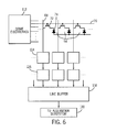
- FIG. 5 a flowchart is represented illustrating a method 100 for operating an imaging system of the type described above.
- an X-ray exposure is initiated by an operator, as represented by step 102 .
- the readout electronics within the detector 22 are activated, as indicated by step 104 .
- an exposure is taken of a patient, whereby X-rays are transmitted through the patient and received by the detector.
- the array of pixels 86 typically measures the intensity of the X-rays received by the detector 22 , via the photodiode provided within each individual pixel.
- the readout electronics typically collect data from the pixels utilizing circuitry associated with each of the data lines, as indicated by step 106 .
- the data are transmitted to a data acquisition subsystem as indicated by step 108 . While data from one specific row of pixels is transmitted to the data acquisition subsystem, signal from the next row of pixels is being converted from analog to digital. Furthermore, pixels from two rows beyond the row being transmitted are being scanned and read. It should be understood that this process continues until the detector 22 , and more particularly all the pixels, are read out. Subsequently, the collected data are processed and ultimately used to reconstruct an image of the exposure area.
- FIG. 6 illustrates a block diagram of certain functional circuitry of a detector and the corresponding readout electronics utilized in an exemplary imaging system.
- FIG. 6 illustrates pixels 54 each comprising a transistor 72 and photodiode 74 .
- a scan line 70 and a data line 68 are also illustrated connected to the respective FET 72 of each of the pixels 54 .
- the scan line 70 is connected to drive electronics 112 .
- each consecutive row of pixels is similarly connected to the drive electronics 112 by a scan line.
- each one of the data lines 68 is connected to a corresponding recharge and measurement subcircuit 114 . It should be noted that each subcircuit 114 restores the charge to each one of the pixels 54 .
- each subcircuit 114 also measures the discharge experienced by the diodes as a result of exposure to radiation. Additionally, each subcircuit 114 is connected to a convert subcircuit 116 .
- the convert subcircuits 116 are configured to convert analog signals received from the pixels 54 to digital signals. It should be understood that each one of the restore/measure subcircuits 114 , are connected to specific convert subcircuit 116 .
- the signals from each convert subcircuits 116 are then transmitted to a line buffer 118 , which comprises part of an output subcircuit, which is not represented in its entirety. Subsequently, the line buffer outputs digital data to the data acquisition subsystem 120 .
- the column or data lines recharge the pixels and measure the discharge of the associated photodiodes.
- the measured data is then transmitted to a convert subcircuit for converting the analog signals to digital signals or data.
- the convert subcircuits transmit the digital signals for each pixel to the line buffer, which collects the data and outputs the collected data for the array of pixels to the data acquisition subsystem 120 .
- FIG. 7 a timing diagram of a normal readout of a detector consisting of “X” rows and “Y” columns is illustrated.
- axis 122 and 124 illustrate the functions of the imaging system 10 .
- Axis 122 represents a pulse pattern for an imaging exposure of a region of interest of a patient, whereby image signals are generated by the detector.
- a signal is provided as illustrated by axis 122 , wherein the detector reads out the signals as indicated by axis 124 .
- the detector reads out a particular detector row, as indicated by axes 126 to 136 , the rows are enabled or activated in sequential order.
- axis 126 illustrates a row 1 as it is activated when the readout of the detector is initiated.
- axis 138 illustrates pulses for a restore function provided by the detector readout electronics.
- axis 138 represents operation of the restore subcircuit 114 as represented in FIG. 6.
- axis 138 illustrates a row-by-row restoration of the charge depleted when the pixels are discharged.
- row 1 is illustrated at a high level along axis 138 when the pixels in row 1 are recharged. Subsequently, following row 1, row 2 are recharged and so on.
- Axis 140 illustrates pulses of a reset function provided by the detector readout electronics. Particularly, the reset signal prepares for the measurement of the rows of pixels. Thus, axis 140 illustrates the reset of the restore subcircuit 114 prior to the restoration of the charge in each pixel of the row that is about to be activated.
- Axis 142 represents pulses of the convert function of the readout electronics. Particularly, the conversion process as illustrated always lags the restoration process by one row or line. Furthermore, it is not until the third row as represented in the present embodiment that the data from the first row, now in digital form after being converted, can be transferred to the acquisition subsystem. The transfer function for several rows is illustrated by axis 144 .
- Axis 146 illustrates the transfer of data from one line.
- an X-ray exposure causes the photodiodes to partially discharge as described above.
- the process of reading out the detector is performed by activating the FET for each pixel in a row, such as beginning with row 1.
- the readout electronics restore the charge on each photodiode to reach the desired voltage.
- the discharge is measured by the readout electronics based upon the charge needed to restore each photodiode to its original charge. For example, as row 2, as represented by axis 138 the charge is restored, the analog signal measured for row 1 is converted as represented along axis 142 .
- row N ⁇ 1 (see axis 130 ) is restored to the original charge as represented by axis 138
- row N ⁇ 2 signals are converted to digital signals (see axis 142 ), and row N ⁇ 3 signals, now in digital form, are transferred to a data acquisition system (see axis 144 ).
- row N ⁇ 2 is illustrated in FIG. 7 as transmitting data signals from channel 1 through channel “X” as illustrated by axis 146 .
- FIG. 8 illustrates a timing diagram for an abbreviated read out of the detectors starting at row N without scrubbing unread rows and transferring all “X” columns of data.
- FIG. 8 shows the readout of the detector 22 of specific rows N through Y, corresponding to axes 132 134 , and 136 respectively.
- row 1, row 2, and row N ⁇ 1 are not active in the scheme illustrated in FIG. 8.
- row N is read out as its charge is restored, as illustrated by restore axis 138 and axis 132 .
- row N+1 is restored to its original charge.
- pixels of row Y are recharged to their original charge as indicated by axis 136 and restore axis 138 .
- a reset signal is applied to the restore/measure subcircuit 114 before actual recharge of the photodiodes for each row occurs as illustrated by axis 140 .
- the conversion of the analog signals to digital signals is accomplished for each row as illustrated by the convert axis 142 .
- the signals from row N are converted to digital signals as row N+1 is being recharged.
- row Y ⁇ 1 signals are being converted to digital signals as photodiodes of row Y are recharged.
- row Y signals are similarly converted to digital signals as illustrated by line 142 .
- the digital signals are transferred to the data acquisition system as represented for a single row by axis 146 .
- signals for row Y ⁇ 2 are transferred to the data channels at the same time signals from row Y ⁇ 1 are being converted from analog to digital form. It should also be understood that at the same time pixels of row Y are being recharged. Similarly, as signals from row Y ⁇ 1 are being transferred to the data channels, signals from row Y are being converted from analog to digital form.
- each function of restoring, converting and transferring the signals produced by the exposure occurs in sequence for individual rows, and partially overlapped in time for the series of rows.
- FIG. 9 illustrates a timing diagram showing an abbreviated read out of a detector starting at row N without scrubbing of unread rows and transferring “X/2” columns of data.
- FIG. 9 illustrates series of axes 122 - 146 . It should be noted that the read out of the detector begins in this implementation at row N as illustrated on axis 132 . As also illustrated, after row N is read out, row N+1 and row Y are readout as illustrated by axes 134 and 136 , respectively. As row N is read out, the photodiodes of the pixels comprising row N are recharged as shown by axis 138 . Subsequently, after a short time delay, row N+1 is recharged.
- the reset of the restore/measure subcircuit 114 prior to the activation of each individual row is illustrated by line 140 .
- pixels of row Y are restored to their original charge.
- the signals received from row N are converted from analog signals to digital signals as illustrated by axis 142 .
- the pixels in row Y are recharged as the data signals from row Y ⁇ 1 are converted from analog signals to digital signals.
- signals from row Y are converted from analog signals to digital signals after a short time delay.
- the signals from row Y ⁇ 1 are being converted from analog to digital form, and pixels of row Y are recharged, the signals from row Y ⁇ 2 are transferred from the detector to the data acquisition system. Specifically, the signals are sent as illustrated by axis 146 . Subsequently, as signals from row Y are being converted to digital signals, signals from row Y ⁇ 1 are transferred to the data channels.
- the present illustration depicts signals transferred from row Y, after similar transfer of signals from row Y ⁇ 1 as illustrated by axis 144 .
- FIG. 10 illustrates a timing diagram showing a reduced field of view consisting of Y rows and “X2” columns.
- row 1 through row Y are activated, as illustrated by axes 126 - 136 .
- Axes 138 - 146 illustrate the restoring, converting, and transferring functions for the detector.
- axis 124 is shown by axes 126 - 144 .
- axes 122 and 124 illustrate the exposure and readout functions of the imaging system 10 .
- Axis 122 represents the imaging system exposing a region of interest of a patient, whereby image signals are generated by the detector. When a patient is exposed to radiation, signals are provided as described above, and the detector reads out the signals as indicated by axis 124 . Thus, as the rows of the detector are read, the rows are activated in sequential order as indicated by axes 126 to 136 . Particularly, axis 126 illustrates row 1 as it is activated when the readout of the detector is initiated. It should be noted that, as before, axis 138 refers to a restore function provided by the detector readout electronics. Axis 138 represents operations of the restore subcircuit 114 as represented in FIG. 6.
- axis 138 illustrates a row-by-row restoration of the charge depleted when the pixels of the detector are discharged by the exposure. For example, row 1 is illustrated at a high along axis 138 when the pixels in row 1 are recharged. After a certain amount of time has elapsed, row 2 is recharged, and so on.
- axis 140 illustrates a reset axis for a reset function provided by the detector readout electronics. The reset signal prepares for the measurement of the rows of pixels.
- axis 140 illustrates the reset of the restore/measure subcircuit 114 for each row prior to the restoration function of the charge in each pixel.
- Axis 142 represents the convert function of the readout electronics.
- the conversion process as illustrated always lags the restoration process by the one row or line. Furthermore, it is not until the third row, as represented in the present embodiment, that the data from the first row, now in digital form after being converted during restoration of the second row, can be transferred to the acquisition subsystem.
- the transfer function is illustrated by axis 144 .
- an X-ray exposure causes the photodiodes to partially discharge as describe earlier.
- the process of reading out the detector is performed by activating the FET for each of the pixels of interest.
- axis 126 is activated as illustrated.
- the readout electronics restore the charge of each photodiode to the desired voltage, and the discharge is measured by the readout electronics. For example, as charges of pixels of row 2 as represented by axis 138 are restored, the analog signals measured for row 1 are converted to digital form as represented in axis 142 .
- row N ⁇ 2 signals are converted to digital signals, and row N ⁇ 3 digital signals are transferred to a data acquisition system.
- signals of row N ⁇ 2 are illustrated in FIG. 10 as being transmitted from channel X/4+1 through channel 3X/4, as illustrated by axis 146 .
- FIG. 11 illustrates a timing diagram representing an abbreviated readout of the detector starting at a row N with scrubbing of unread rows in parallel and transferring all “X” columns of data.
- FIG. 11 shows the read out of the detector 22 by specific rows N ⁇ 1, N, N+1 and Y with respect to axes 130 , 132 , 134 and 136 .
- row 1 and row 2 are active in this implementation. Specifically, during the time that the detector is being exposed, pixels of rows 1 and 2 are scrubbed. Thus, the charge for pixels of these rows is restored, however data is not measured and collected. It should be noted that a short time delay is provided before each restore function, as illustrated by axis 140 .
- pixels of row N+1 represented by axis 134 are restored to their original charge.
- pixels of row Y are recharged as indicated by axis 136 and restore axis 138 .
- a reset signal is applied to the restore subcircuit before actual recharge of the photodiodes in each row occurs as illustrated by axis 140 .
- the conversion of the analog signals to digital signals is accomplished for each row as illustrated by the convert axis 142 . Specifically, the signals from row N are converted to digital signals as row N+1 is being recharged. Similarly, row Y ⁇ 1 signals are converted to digital signals as row Y photodiodes are recharged. Further, row Y signals are converted to digital signals as illustrated by line 142 .
- the converted digital signals are transferred to the data acquisition system as represented by axis 146 .
- data for row Y ⁇ 2 are transferred to the detector controller 26 at the same time as signals of row Y ⁇ 1 are being converted from analog to digital form.
- row Y pixels are being recharged to their original charge.
- row Y signals being converted from analog to digital form.
- FIG. 12 is a flow chart representing the process of the present technique.
- an initial X-ray exposure is taken of a subject of interest.
- the detector 22 receives a portion of the radiation, following which the read out of the detector is initiated as indicated by step 152 .
- the read out of the detector is initiated by the control system.
- the read out of the detector comprises reset of the restore subcircuit prior to readout of each row as shown by step 154 , and restoring the charge on each photodiode of the pixels as indicated by step 156 .
- the analog signals measured are converted to digital signals as illustrated by step 158 .
- the read out of the detector provides the transfer of the digital signals from the detector electronics to the data acquisition subsystem as indicated by step 160 . Once restoration of that specific row is accomplished, the read out for that row is deactivated as illustrated by step 164 .
- step 166 the read out of the subsequent row is activated as shown by step 166 . Similar to the previous row, read out of the next row of pixels is performed by initiating the reset, restore, convert, and transfer functions, producing an output is indicated by steps 168 - 176 . Again, once that specific row is readout, the row is subsequently deactivated as illustrated by step 178 . Next, the system generally checks whether the next row is the last row to be read as indicated by step 180 . If the row just read out was the last row, then the read out of the detector is ended as indicated by step 182 . Otherwise, the read out of the next row is activated as illustrated by step 166 .
- FIG. 13 illustrates stages in carrying out the process, similar to that described above, in a present implementation.
- code for controlling the scanning, converting and transferring functions begins at a step 186 in which a row variable, called “next row” in the example, is set to an initial value called “first row.”
- the exposure is made as described above. It should be noted that various types of exposure may be made, including pulsed and continuous exposures.
- a recharge sub-circuit is reset as indicated at step 190 .
- the row currently designated as the “next row” is enabled for readout as indicated at step 192 .
- a waiting period is then initiated as indicated at step 194 , and a sufficient time is allowed to pass for complete recharge of the pixels of the row.
- the “next row” is disabled and measurement is completed as shown at step 196 .
- step 196 the simultaneous operations described above take place through the remainder of the process. That is, as shown at step 198 , the measured data for the “next row” resulting from step 196 is converted to digital values. It should be noted that this conversion is performed for all channels of the readout electronics in parallel. Following the conversion, the data is output to the acquisition system at step 200 , in a manner described above.
- the readout continues as indicated at step 202 in FIG. 13.
- the control code determines whether the “next row” is the “last row” of the detector to be scanned. If the last desired scanned row is not the current value of “next row” the process reverts to step 204 at which the value of “next row” is indexed. With the indexed value of the variable “new row” then, control reverts to step 190 for recharging of the pixels of the row, measurement, conversion and transfer.
- step 206 the controller awaits completion of the conversion and output of the last row recharged.
- the readout is indicated as complete, and control may revert to step 186 for the next examination.
- the drive electronics of the detector are implemented as a shift register with a high voltage output in conjunction with a separate input.
- a single bit is shifted into the shift register.
- an input signal is activated and the output of the drive electronics associated with the first row is placed in an “ON” state.
- the transistor within the each pixel conducts and the restore subcircuit provides the charge necessary to fully restore the photodiodes of the pixels on the first row.
- the activated input signal is taken to its inactive state, causing the output to return to an “OFF” state, and the pixel transistors become non-conducting.
- the shift register is clocked and the internal bit is advanced from the first position to the second. As the first bit is shifted, the sequence for driving the successive rows would be: enable, disable, shift, enable, disable, shift, enable, and disable, and so forth.
- the detector is provided a function to allow scrubbing to prevent the characteristics of the individual pixels from degrading over time.
- rows of pixels that are not being scanned as part of the reduced field of view can be scrubbed during the exposure at which time the field of view is not being read. More than one row can be scrubbed at a time.
- a small amount of time during every image read out is provided for scrubbing as mentioned above, so that rows outside the field of view may be scrubbed.
- Another alternative implementation allows scrubbing and reading out more than one row at a time. Furthermore, the time for each row can be minimized by transferring only the data that is part of the field of view.
- restricting the field of view saves readout time in two ways: firstly, by reducing the number of rows that need to be read out, and secondly, by reducing the number of data channels of data that need to be transferred in each row It should be noted again that other tradeoffs between measurement and conversion may be possible.
- a restricted field of view is defined along the edge of the detector (as opposed to the center)
- another advantage of the invention that is gained is that of improved angulation in positioning the patient relative to the detector. Defining a restricted field of view along the edge of the detector allows the detector to be positioned closer to the patient in procedures that require the detection of X-Rays produced at angles other than “normal” to the patient.
Landscapes
- Engineering & Computer Science (AREA)
- Multimedia (AREA)
- Signal Processing (AREA)
- Measurement Of Radiation (AREA)
- Apparatus For Radiation Diagnosis (AREA)
- Magnetic Resonance Imaging Apparatus (AREA)
- Transforming Light Signals Into Electric Signals (AREA)
Abstract
Description
- The present invention relates generally to imaging systems, such as radiographic systems, and more particularly, to digital detectors used in such systems. Even more particularly, the present invention relates to an apparatus and method for reducing time involved in reading a solid state X-ray detector.
- Digital imaging systems are becoming increasingly widespread for producing digital data which can be reconstructed into useful radiographic images. In one application of a digital imaging system, radiation from a source is directed toward a subject, typically a patient in a medical diagnostic application, and a portion of the radiation passes through the subject and impacts a detector. The surface of the detector converts the radiation to light photons, which are sensed.
- The detector is divided into an array of discrete picture elements or pixels, and encodes output signals based upon the quantity or intensity of the radiation impacting each pixel region. Because the radiation intensity is altered as the radiation passes through the subject, the images reconstructed based upon the output signals may provide a projection of tissues and other features similar to those available through conventional photographic film techniques.
- In available digital detectors, the detector surface is divided into an array of picture elements or pixels, with rows and columns of pixels being organized adjacent to one another to form the overall image area. When the detector is exposed to radiation, photons impact a scintillator coextensive with the image area. A series of detector elements are formed at row and column crossing points, each crossing point corresponding to a pixel making up the image matrix. In one type of detector, each element consists of a photodiode and a thin film transistor. The transistors and photodiodes are typically constructed of amorphous silicon, over which cesium iodide is deposited. The cesium iodide absorbs the X-rays and converts them to light, which is then detected by the photodiodes. As can be appreciated by those skilled in the art, the photodiode acts as a capacitor, where the photodiode is generally charged to some known voltage. Light that is emitted in proportion to the X-ray flux then partially discharges the photodiode. Once the exposure is completed, charge on the photodiode is restored to the initial charge. The amount of charge required to restore the initial voltage on the photodiode is then measured which becomes a measure of the X-ray radiation impacting the pixel during the length of the exposure.
- In a detector of the type described above, the cathode of each photodiode is connected to the source of a transistor, and the anodes of all diodes are connected to a negative bias voltage. Further, the gates of the transistors in a row are connected together and a row electrode is connected to scanning electronics. The drains of the transistors in each column are connected together and each column electrode is connected to additional readout electronics. Sequential scanning of the rows and simultaneous read out of the signals present at the column electrode permits the system to acquire the entire array or matrix of signals for subsequent signal processing and display. Thus, the detector is read or “scrubbed” on a row-by-row basis as controlled by the transistor associated with each photodiode. It should be noted that reading of the detector refers to recharging of the photodiodes and collection of data when the image produced by the detector contains valuable data, mainly images that contain exposure or offset data, whereas “scrubbing” refers to similar recharging even though the data is not important and can be discarded or not collected at all. Scrubbing, therefore is executed to restore the charge on the photodiode. More importantly, scrubbing is performed to maintain a proper bias on the diodes during idle periods or to reduce the effects of lag, which is an incomplete charge restoration of the photodiodes. Thus, scrubbing is typically performed to restore and maintain the charge of the photodiode, in addition to preventing a continuous DC voltage bias on the amorphous silicon transistors.
- The detector is typically read or scrubbed according to its array structure, that is, on a row-by-row basis. As mentioned above, the reading or scrubbing of the detector is controlled by field effect transistors (FETs) associated with each photodiode. The FET allows the minimization of the number of electrical contacts that would need to made to the detector. Thus, the FETs reduce the number of required contacts to no more than the number of pixels along the perimeter of the array. Further, an entire row of an array may be controlled simultaneously when the scan line attached to the gates of all the FETs of pixels on that particular row is activated. It should be noted that each of the pixels on the particular row is connected to a separate data line through a FET, which is used by the readout electronics to restore the charge to the photodiodes. Thus, as each row is activated or read-enabled, the charge is restored for each pixel in that row simultaneously by the read out electronics over the individual data line for each column. Thus, each data line has a dedicated read out channel associated with it.
- In use, the signals generated at the pixel locations of the detector are sampled and digitized. The digital values are transmitted to processing circuitry where they are filtered, scaled, and further processed to produce the image data set. The data set may then be used to reconstruct the resulting image, to display the image, such as on a computer monitor, to transfer the image to conventional photographic film, and so forth. In the medical imaging field, such images are used by attending physicians and radiologists in evaluating the physical conditions of a patient and diagnosing disease and trauma.
- Large area solid-state detector arrays, such as those described above, provide solutions for digital imaging applications such as medical imaging, digital reproduction and non-destructive testing. While such detectors provide excellent image data, further improvement is needed. For instance, a detector having a small pixel size providing high spatial resolution comes at the cost of acquisition frame rate. Furthermore, for a given pixel size, a larger detector is generally more expensive due to the cost of the required support electronics, and will not support frame rates as fast as a smaller detector with the same bandwidth. Many times, when a specific application is targeted, detector design tradeoffs are made to optimize the detector's performance in regards to that application. One result of this is that larger detectors with small pixels typically do not have the bandwidth to support higher frame rates.
- There is a need, therefore, for a technique designed to increase the acquisition frame rate without affecting other variables that reduce image quality.
- The present invention features a digital detector design that addresses such needs. One aspect of the technique provides a method for acquiring signals from discrete pixels in a detector. The detector includes a matrix of rows and columns of pixels, whereby each pixel is configured to generate a signal based upon the radiation received from a radiation source and at improved frame rates.
- Another aspect of the technique relates to an imaging system including a source of radiation, a control circuit to regulate the source of radiation, and a detector for receiving radiation from the source and for generating signals therefrom. The detector has an array of pixels, forming rows and columns coupled to a plurality of scan lines, each scan line being coupled to a plurality of rows of pixels. The detector is configured to process the exposure in a reduced field of view.
- Yet another aspect of the technique relates to a detector comprising an array of pixels in rows and columns, configured to generate signals based upon radiation impacting the detector. The detector also has a plurality of scan lines, wherein each scan line is coupled to a plurality of rows of pixels. Additionally, the pixels of the array are coupled to a series of data lines, so that when the pixels are scanned, the data generated by the scan are transmitted via the data lines to a data acquisition subsystem.
- FIG. 1 is a diagrammatical overview of a digital X-ray imaging system in which the present technique may be utilized;
- FIG. 2 is a diagrammatical representation of the functional circuitry in a detector of the system of FIG. 1 to produce image data for reconstruction;
- FIG. 3 is a partial sectional view illustrating an exemplary detector structure for producing the image data;
- FIG. 4 is a circuit schematic illustrating rows and columns of pixels in an exemplary detector;
- FIG. 5 is a flowchart representing the method of operating an exemplary imaging system for providing image data;
- FIG. 6 is a block diagram of the representing the connectivity of an exemplary detector;
- FIG. 7 is a timing diagram illustrating a readout operation of an exemplary detector;
- FIG. 8 is a timing diagram illustrating a readout operation utilized by the present technique;
- FIG. 9 is a timing diagram illustrating an alternative readout operation as illustrated in FIG. 8;
- FIG. 10 is a timing diagram illustrating a readout operation of a reduced field of view in an exemplary detector;
- FIG. 11 is timing diagram illustrating the present technique of initiating a readout operation and scrubbing operation simultaneously;
- FIG. 12 is flowchart illustrating exemplary steps utilized in performing the present technique; and
- FIG. 13 is a flow chart illustrating in somewhat greater detail specific stages in performing the present technique in accordance with a present implementation.
- FIG. 1 illustrates diagrammatically an
imaging system 10 for acquiring and processing discrete pixel image data. In the illustrated embodiment,system 10 is a digital X-ray system designed both to acquire original image data and to process the image data for display in accordance with the present technique. In the embodiment illustrated in FIG. 1,imaging system 10 includes a source ofX-ray radiation 12 positioned adjacent to acollimator 14.Collimator 14 permits a stream ofradiation 16 to pass into a region in which a subject, such as ahuman patient 18 is positioned. A portion of theradiation 20 passes through or around the subject and impacts a digital X-ray detector, represented generally atreference numeral 22. As described more fully below,detector 22 converts the X-ray photons received on its surface to lower energy photons, and subsequently to electric signals, which are acquired and processed to reconstruct an image of the features within the subject. -
Source 12 is controlled by a power supply/control circuit 24 which furnishes both power and control signals for examination sequences. Moreover,detector 22 is coupled to adetector controller 26 which commands acquisition of the signals generated in thedetector 22.Detector controller 26 may also execute various signal processing and filtration functions, such as for initial adjustment of dynamic ranges, interleaving of digital image data, and so forth. Both power supply/control circuit 24 anddetector controller 26 are responsive to signals from asystem controller 28. In general,system controller 28 commands operation of the imaging system to execute examination protocols and to process acquired image data. In the present context,system controller 28 also includes signal processing circuitry, typically based upon a general purpose or application-specific digital computer, associated memory circuitry for storing programs and routines executed by the computer, as well as configuration parameters and image data, interface circuits, and so forth. - In the embodiment illustrated in FIG. 1,
system controller 28 is linked to at least one output device, such as a display or printer as indicated atreference numeral 30. The output device may include standard or special purpose computer monitors and associated processing circuitry. One ormore operator workstations 32 may be further linked in the system for outputting system parameters, requesting examinations, viewing images, and so forth. In general, displays, printers, workstations, and similar devices supplied within the system may be local to the data acquisition components, or may be remote from these components, such as elsewhere within an institution or hospital, or in an entirely different location, linked to the image acquisition system via one or more configurable networks, such as the Internet, virtual private networks, and so forth. - FIG. 2 is a diagrammatical representation of functional components of
digital detector 22. FIG. 2 also represents an imaging detector controller orIDC 34 which will typically be configured withindetector controller 26.IDC 34 includes a CPU or digital signal processor, as well as memory circuits for commanding acquisition of sensed signals from the detector.IDC 34 is coupled via two-way fiberoptic conductors to detector control circuitry 36 withindetector 22.IDC 34 thereby exchanges command signals for image data within the detector during operation. - Detector control circuitry 36 receives DC power from a power source, represented generally at
reference numeral 38. Detector control circuitry 36 is configured to originate timing and control commands for row and column electronics used to acquire image data during data acquisition phases of operation of the system. Circuitry 36 therefore transmits power and control signals to reference/regulator circuitry 40, and receives digital image pixel data fromcircuitry 40. - In a present embodiment,
detector 22 consists of a scintillator that converts X-ray photons received on the detector surface during examinations to lower energy (light) photons. An array of photodetectors then converts the light photons to electrical signals which are representative of the number of photons or the intensity of radiation impacting individual pixel regions of the detector surface. Readout electronics convert the resulting analog signals to digital values that can be processed, stored, and displayed, such as in adisplay 30 or aworkstation 32 following reconstruction of the image. In a present form, the array of photodetectors is formed of amorphous silicon. The array elements are organized in rows and columns, with each element consisting of a photodiode and a thin film transistor. The cathode of each diode is connected to the source of the transistor, and the anodes of all diodes are connected to a negative bias voltage. The gates of the transistors in each row are connected together and the row electrodes are connected to the scanning electronics as described below. The drains of the transistors in a column are connected together and the electrode of each column is connected to an individual channel of the readout electronics. - In the particular embodiment illustrated in FIG. 2, by way of example, a
row bus 42 includes a plurality of conductors for enabling readout from various rows of the detector, as well as for disabling rows and applying a charge compensation voltage to selected rows, where desired. Acolumn bus 44 includes additional conductors for commanding readout from the columns while the rows are sequentially enabled.Row bus 42 is coupled to a series ofrow drivers 46, each of which commands enabling of a series of rows in the detector. Similarly,readout electronics 48 are coupled tocolumn bus 44 for commanding readout of all columns of the detector. In the present technique, image acquisition rate is increased by employing a partial readout of thedetector 22. - In the illustrated embodiment,
row drivers 46 andreadout electronics 48 are coupled to adetector panel 50 which may be subdivided into a plurality ofsections 52. Eachsection 52 is coupled to one of therow drivers 46, and includes a number of rows. Similarly, eachcolumn driver 48 is coupled to a series of columns. The photodiode and thin film transistor arrangement mentioned above thereby define a series of pixels ordiscrete picture elements 54 which are arranged inrows 56 andcolumns 58. The rows and columns define animage matrix 60, having aheight 62 and awidth 64. Again, as described below, the present technique allows an enhanced number of pixels to be read out via the row drivers and column readout electronics. - As also illustrated in FIG. 2, each
pixel 54 is generally defined at a row and column crossing, at which acolumn electrode 68 crosses arow electrode 70. As mentioned above, athin film transistor 72 is provided at each crossing location for each pixel, as is aphotodiode 74. As each row is enabled byrow drivers 46, signals from eachphotodiode 74 may be accessed viareadout electronics 48, and converted to digital signals for subsequent processing and image reconstruction. Thus, an entire row of pixels in the array is controlled simultaneously when the scan line attached to the gates of all the transistors of pixels on that row is activated. Consequently, each of the pixels in that particular row is connected to a data line, through a switch, which is used by the readout electronics to restore the charge to thephotodiode 74. - It should be noted that as the charge is restored to all the pixels in one row simultaneously by each of the associated dedicated readout channels, the readout electronics is converting the measurements from the previous row from an analog voltage to a digital value. Furthermore, the readout electronics are transferring the digital values from 2 rows previous to the acquisition subsystem, which will perform some processing prior to displaying a diagnostic image on a monitor or writing it to film. Thus, the read out electronics are performing three functions simultaneously; measuring or restoring the charge for the pixels in a particular row, converting the data for pixels in the previous row and transferring the converted data for the pixels in a twice previous row.
- FIG. 3 generally represents an exemplary physical arrangement of the components illustrated diagrammatically in FIG. 2. As shown in FIG. 3, the detector may include a
glass substrate 76 on which the components described below are disposed.Column electrodes 68 androw electrodes 70 are provided on the substrate, and an amorphous siliconflat panel array 78 is defined, including the thin film transistors and photodiodes described above. Ascintillator 80 is provided over the amorphous silicon array for receiving radiation during examination sequences as described above. Contactfingers 82 are formed for communicating signals to and from the column and row electrodes, and contact leads 84 are provided for communicating the signals between the contact fingers and external circuitry. - It should be noted that the particular configuration of the
detector panel 22, and the subdivision of the panel into rows and columns controlled by row drivers and column read out channels is subject to various alternate configurations. In particular, more or fewer row drivers and column read out channels may be used, and detector panels having various matrix dimensions may thereby be defined. Thedetector panel 22 may be further subdivided into regions of multiple sections, such as along a vertical or horizontal center line. - It should be further noted that the readout electronics in the detector generally employ a pipeline type architecture. For example, as the charge is restored to all the pixels in a particular row simultaneously by each of the associated dedicated readout channels, the readout electronics convert the measurements from the previous row from an analog signal to a digital signal. Concurrently, the readout electronics transfer the measured digital values from two rows previous to the data acquisition subsystem. The data acquisition subsystem typically performs some processing prior to displaying a diagnostic image on a display. Thus, the readout electronics in the present technique perform three functions simultaneously.
- FIG. 4 illustrates an array of
pixels 86 located on an exemplary detector having a plurality of column lines and row lines. As illustrated by the array ofpixels 86, each pixel comprises thetransistor 72 and thephotodiode 74. It should be noted that the array is made up of a plurality ofscan lines data lines scan lines - As illustrated, scan line 88(denoted N in FIG. 4) is connected to each one of the pixels in that specific row. Additionally,
scan line 88 is capacitively coupled to each of one of the data lines by virtue of both the scan/data line crossover and the capacitance between the gate and the drain of the pixel FET. For example,scan line 88 is capacitively coupled to data line 94 (denoted K in FIG. 4) and data line 98 (K+1). Similarly, each one of the data lines is capacitively coupled to each one of the scan lines. Thus, as illustrated for the array ofpixels 86, scan line 88 (N), scan line 90 (N−1), and scan line 92 (N+1) are capacitively coupled to data line 94 (K), data line 96 (K−1), and data line 98 (K+1) and so on. It should be understood that each data line is typically connected to one specific column of pixels and each scan line is connected to one specific row of pixels. Additionally, although in the present embodiment of FIG. 4, 30 pixels are illustrated, it should be noted that additional pixels may, of course, be incorporated in the pixel array. - Turning to FIG. 5, a flowchart is represented illustrating a
method 100 for operating an imaging system of the type described above. Initially, an X-ray exposure is initiated by an operator, as represented bystep 102. Once an X-ray exposure is completed, the readout electronics within thedetector 22 are activated, as indicated bystep 104. As mentioned above, an exposure is taken of a patient, whereby X-rays are transmitted through the patient and received by the detector. The array ofpixels 86 typically measures the intensity of the X-rays received by thedetector 22, via the photodiode provided within each individual pixel. The readout electronics typically collect data from the pixels utilizing circuitry associated with each of the data lines, as indicated bystep 106. Once the data are collected for a particular row of pixels, the data are transmitted to a data acquisition subsystem as indicated bystep 108. While data from one specific row of pixels is transmitted to the data acquisition subsystem, signal from the next row of pixels is being converted from analog to digital. Furthermore, pixels from two rows beyond the row being transmitted are being scanned and read. It should be understood that this process continues until thedetector 22, and more particularly all the pixels, are read out. Subsequently, the collected data are processed and ultimately used to reconstruct an image of the exposure area. - FIG. 6 illustrates a block diagram of certain functional circuitry of a detector and the corresponding readout electronics utilized in an exemplary imaging system. Particularly, FIG. 6 illustrates
pixels 54 each comprising atransistor 72 andphotodiode 74. Ascan line 70 and adata line 68 are also illustrated connected to therespective FET 72 of each of thepixels 54. It should be further noted that thescan line 70 is connected to driveelectronics 112. It should be noted that each consecutive row of pixels is similarly connected to thedrive electronics 112 by a scan line. On the other hand, each one of the data lines 68 is connected to a corresponding recharge andmeasurement subcircuit 114. It should be noted that eachsubcircuit 114 restores the charge to each one of thepixels 54. Further each subcircuit 114 also measures the discharge experienced by the diodes as a result of exposure to radiation. Additionally, eachsubcircuit 114 is connected to aconvert subcircuit 116. Theconvert subcircuits 116 are configured to convert analog signals received from thepixels 54 to digital signals. It should be understood that each one of the restore/measure subcircuits 114, are connected tospecific convert subcircuit 116. The signals from eachconvert subcircuits 116 are then transmitted to aline buffer 118, which comprises part of an output subcircuit, which is not represented in its entirety. Subsequently, the line buffer outputs digital data to thedata acquisition subsystem 120. - Thus, to summarize, as the
drive electronics 112 scan each row of pixels, the column or data lines recharge the pixels and measure the discharge of the associated photodiodes. The measured data is then transmitted to a convert subcircuit for converting the analog signals to digital signals or data. Next, the convert subcircuits transmit the digital signals for each pixel to the line buffer, which collects the data and outputs the collected data for the array of pixels to thedata acquisition subsystem 120. - Turning to FIG. 7, a timing diagram of a normal readout of a detector consisting of “X” rows and “Y” columns is illustrated. Particularly,
axis imaging system 10.Axis 122 represents a pulse pattern for an imaging exposure of a region of interest of a patient, whereby image signals are generated by the detector. At the time of the image exposure, a signal is provided as illustrated byaxis 122, wherein the detector reads out the signals as indicated byaxis 124. Thus, when the detector reads out a particular detector row, as indicated by axes 126 to 136, the rows are enabled or activated in sequential order. Particularly, axis 126 illustrates arow 1 as it is activated when the readout of the detector is initiated. It should be noted thataxis 138 illustrates pulses for a restore function provided by the detector readout electronics. Specifically,axis 138 represents operation of the restoresubcircuit 114 as represented in FIG. 6. Further,axis 138 illustrates a row-by-row restoration of the charge depleted when the pixels are discharged. For example,row 1 is illustrated at a high level alongaxis 138 when the pixels inrow 1 are recharged. Subsequently, followingrow 1,row 2 are recharged and so on. -
Axis 140 illustrates pulses of a reset function provided by the detector readout electronics. Particularly, the reset signal prepares for the measurement of the rows of pixels. Thus,axis 140 illustrates the reset of the restoresubcircuit 114 prior to the restoration of the charge in each pixel of the row that is about to be activated.Axis 142 represents pulses of the convert function of the readout electronics. Particularly, the conversion process as illustrated always lags the restoration process by one row or line. Furthermore, it is not until the third row as represented in the present embodiment that the data from the first row, now in digital form after being converted, can be transferred to the acquisition subsystem. The transfer function for several rows is illustrated byaxis 144.Axis 146 illustrates the transfer of data from one line. - Thus, in the example, an X-ray exposure causes the photodiodes to partially discharge as described above. At the conclusion of the exposure, the process of reading out the detector is performed by activating the FET for each pixel in a row, such as beginning with
row 1. As each row is read, as for axis 126 as illustrated, the readout electronics restore the charge on each photodiode to reach the desired voltage. The discharge is measured by the readout electronics based upon the charge needed to restore each photodiode to its original charge. For example, asrow 2, as represented byaxis 138 the charge is restored, the analog signal measured forrow 1 is converted as represented alongaxis 142. Next, as row N−1 (see axis 130) is restored to the original charge as represented byaxis 138, row N−2 signals are converted to digital signals (see axis 142), and row N−3 signals, now in digital form, are transferred to a data acquisition system (see axis 144). Particularly, row N−2 is illustrated in FIG. 7 as transmitting data signals fromchannel 1 through channel “X” as illustrated byaxis 146. - FIG. 8 illustrates a timing diagram for an abbreviated read out of the detectors starting at row N without scrubbing unread rows and transferring all “X” columns of data. Particularly, FIG. 8 shows the readout of the
detector 22 of specific rows N through Y, corresponding toaxes 132 134, and 136 respectively. It should be noted thatrow 1,row 2, and row N−1 are not active in the scheme illustrated in FIG. 8. Thus, as described above forrow 1, row N is read out as its charge is restored, as illustrated by restoreaxis 138 andaxis 132. After a short time delay row N+1 is restored to its original charge. Subsequently, pixels of row Y are recharged to their original charge as indicated byaxis 136 and restoreaxis 138. It should be further noted that a reset signal is applied to the restore/measure subcircuit 114 before actual recharge of the photodiodes for each row occurs as illustrated byaxis 140. In the present embodiment, the conversion of the analog signals to digital signals is accomplished for each row as illustrated by theconvert axis 142. Specifically, the signals from row N are converted to digital signals as row N+1 is being recharged. Similarly, row Y−1 signals are being converted to digital signals as photodiodes of row Y are recharged. Further, row Y signals are similarly converted to digital signals as illustrated byline 142. - Next, the digital signals are transferred to the data acquisition system as represented for a single row by
axis 146. In the illustrated embodiment, signals for row Y−2 are transferred to the data channels at the same time signals from row Y−1 are being converted from analog to digital form. It should also be understood that at the same time pixels of row Y are being recharged. Similarly, as signals from row Y−1 are being transferred to the data channels, signals from row Y are being converted from analog to digital form. Thus, as can be seen by the illustration in FIG. 8 each function of restoring, converting and transferring the signals produced by the exposure occurs in sequence for individual rows, and partially overlapped in time for the series of rows. - FIG. 9 illustrates a timing diagram showing an abbreviated read out of a detector starting at row N without scrubbing of unread rows and transferring “X/2” columns of data. FIG. 9 illustrates series of axes 122-146. It should be noted that the read out of the detector begins in this implementation at row N as illustrated on
axis 132. As also illustrated, after row N is read out, row N+1 and row Y are readout as illustrated byaxes axis 138. Subsequently, after a short time delay, row N+1 is recharged. The reset of the restore/measure subcircuit 114 prior to the activation of each individual row is illustrated byline 140. Subsequently, after a short period of time, pixels of row Y are restored to their original charge. Further, as the pixels of row N+1 are being recharged, the signals received from row N are converted from analog signals to digital signals as illustrated byaxis 142. Next, the pixels in row Y are recharged as the data signals from row Y−1 are converted from analog signals to digital signals. Similarly, signals from row Y are converted from analog signals to digital signals after a short time delay. Thus, as the signals from row Y−1 are being converted from analog to digital form, and pixels of row Y are recharged, the signals from row Y−2 are transferred from the detector to the data acquisition system. Specifically, the signals are sent as illustrated byaxis 146. Subsequently, as signals from row Y are being converted to digital signals, signals from row Y−1 are transferred to the data channels. The present illustration depicts signals transferred from row Y, after similar transfer of signals from row Y−1 as illustrated byaxis 144. - FIG. 10 illustrates a timing diagram showing a reduced field of view consisting of Y rows and “X2” columns. In this illustration,
row 1 through row Y are activated, as illustrated by axes 126-136. Axes 138-146 illustrate the restoring, converting, and transferring functions for the detector. Thus, it should be noted that the read out of the detector as illustrated byaxis 124 is shown by axes 126-144. In the present diagram the read out ofrows 1 through Y is illustrated. Similarly to the procedure discussed above, axes 122 and 124 illustrate the exposure and readout functions of theimaging system 10.Axis 122 represents the imaging system exposing a region of interest of a patient, whereby image signals are generated by the detector. When a patient is exposed to radiation, signals are provided as described above, and the detector reads out the signals as indicated byaxis 124. Thus, as the rows of the detector are read, the rows are activated in sequential order as indicated by axes 126 to 136. Particularly, axis 126 illustratesrow 1 as it is activated when the readout of the detector is initiated. It should be noted that, as before,axis 138 refers to a restore function provided by the detector readout electronics.Axis 138 represents operations of the restoresubcircuit 114 as represented in FIG. 6. Further,axis 138 illustrates a row-by-row restoration of the charge depleted when the pixels of the detector are discharged by the exposure. For example,row 1 is illustrated at a high alongaxis 138 when the pixels inrow 1 are recharged. After a certain amount of time has elapsed,row 2 is recharged, and so on. Next,axis 140 illustrates a reset axis for a reset function provided by the detector readout electronics. The reset signal prepares for the measurement of the rows of pixels. Thus,axis 140 illustrates the reset of the restore/measure subcircuit 114 for each row prior to the restoration function of the charge in each pixel.Axis 142 represents the convert function of the readout electronics. The conversion process as illustrated always lags the restoration process by the one row or line. Furthermore, it is not until the third row, as represented in the present embodiment, that the data from the first row, now in digital form after being converted during restoration of the second row, can be transferred to the acquisition subsystem. The transfer function is illustrated byaxis 144. - Thus, in the example, an X-ray exposure causes the photodiodes to partially discharge as describe earlier. At the conclusion of the exposure, the process of reading out the detector is performed by activating the FET for each of the pixels of interest. As represented by FIG. 10, axis 126 is activated as illustrated. Simultaneously, the readout electronics restore the charge of each photodiode to the desired voltage, and the discharge is measured by the readout electronics. For example, as charges of pixels of
row 2 as represented byaxis 138 are restored, the analog signals measured forrow 1 are converted to digital form as represented inaxis 142. Next, as charges of pixels of row N−1 are restored as represented byaxis 138, row N−2 signals are converted to digital signals, and row N−3 digital signals are transferred to a data acquisition system. Particularly, signals of row N−2 are illustrated in FIG. 10 as being transmitted from channel X/4+1 throughchannel 3X/4, as illustrated byaxis 146. - FIG. 11 illustrates a timing diagram representing an abbreviated readout of the detector starting at a row N with scrubbing of unread rows in parallel and transferring all “X” columns of data. FIG. 11 shows the read out of the
detector 22 by specific rows N−1, N, N+1 and Y with respect toaxes row 1 androw 2 are active in this implementation. Specifically, during the time that the detector is being exposed, pixels ofrows axis 140. Thus, after a short time delay charges of pixels of row N+1 represented byaxis 134 are restored to their original charge. Subsequently, pixels of row Y are recharged as indicated byaxis 136 and restoreaxis 138. It should be further noted that a reset signal is applied to the restore subcircuit before actual recharge of the photodiodes in each row occurs as illustrated byaxis 140. In the present embodiment, the conversion of the analog signals to digital signals is accomplished for each row as illustrated by theconvert axis 142. Specifically, the signals from row N are converted to digital signals as row N+1 is being recharged. Similarly, row Y−1 signals are converted to digital signals as row Y photodiodes are recharged. Further, row Y signals are converted to digital signals as illustrated byline 142. - As mentioned previously, the converted digital signals are transferred to the data acquisition system as represented by
axis 146. In this implementation, data for row Y−2 are transferred to thedetector controller 26 at the same time as signals of row Y−1 are being converted from analog to digital form. It should also be understood that, concurrently, row Y pixels are being recharged to their original charge. Similarly, as data for row Y−1 are being transferred to thedetector controller 26, row Y signals being converted from analog to digital form. Thus, as can be seen by the illustration in FIG. 11, each function of restoring, converting and transferring the signals produced by the exposure of the X-ray beam occurs sequentially for each row, and overlapped in time for the series of rows read from the detector. - FIG. 12 is a flow chart representing the process of the present technique. As indicated by
step 150, an initial X-ray exposure is taken of a subject of interest. As the exposure is taken, thedetector 22 receives a portion of the radiation, following which the read out of the detector is initiated as indicated bystep 152. It should be noted that the read out of the detector is initiated by the control system. The read out of the detector comprises reset of the restore subcircuit prior to readout of each row as shown bystep 154, and restoring the charge on each photodiode of the pixels as indicated bystep 156. Further, the analog signals measured are converted to digital signals as illustrated bystep 158. The read out of the detector provides the transfer of the digital signals from the detector electronics to the data acquisition subsystem as indicated bystep 160. Once restoration of that specific row is accomplished, the read out for that row is deactivated as illustrated bystep 164. - Next, the read out of the subsequent row is activated as shown by
step 166. Similar to the previous row, read out of the next row of pixels is performed by initiating the reset, restore, convert, and transfer functions, producing an output is indicated by steps 168-176. Again, once that specific row is readout, the row is subsequently deactivated as illustrated bystep 178. Next, the system generally checks whether the next row is the last row to be read as indicated bystep 180. If the row just read out was the last row, then the read out of the detector is ended as indicated bystep 182. Otherwise, the read out of the next row is activated as illustrated bystep 166. - FIG. 13 illustrates stages in carrying out the process, similar to that described above, in a present implementation. In the implemented process, indicated generally by
reference numeral 184 in FIG. 13, code for controlling the scanning, converting and transferring functions begins at astep 186 in which a row variable, called “next row” in the example, is set to an initial value called “first row.” Atstep 188 the exposure is made as described above. It should be noted that various types of exposure may be made, including pulsed and continuous exposures. - With the exposure made, and the detector having been altered by the radiation incident thereon during the exposure, a recharge sub-circuit is reset as indicated at
step 190. Subsequently, the row currently designated as the “next row” is enabled for readout as indicated atstep 192. A waiting period is then initiated as indicated atstep 194, and a sufficient time is allowed to pass for complete recharge of the pixels of the row. Following this waiting period, the “next row” is disabled and measurement is completed as shown atstep 196. - Following
step 196, the simultaneous operations described above take place through the remainder of the process. That is, as shown atstep 198, the measured data for the “next row” resulting fromstep 196 is converted to digital values. It should be noted that this conversion is performed for all channels of the readout electronics in parallel. Following the conversion, the data is output to the acquisition system atstep 200, in a manner described above. - While the conversion and transfer operations are being accomplished, the readout continues as indicated at
step 202 in FIG. 13. In particular, the control code determines whether the “next row” is the “last row” of the detector to be scanned. If the last desired scanned row is not the current value of “next row” the process reverts to step 204 at which the value of “next row” is indexed. With the indexed value of the variable “new row” then, control reverts to step 190 for recharging of the pixels of the row, measurement, conversion and transfer. Once the last row to be scanned is recharged, causing the result atstep 202 to be affirmative, the process proceeds to step 206 at which the controller awaits completion of the conversion and output of the last row recharged. Atstep 208 the readout is indicated as complete, and control may revert to step 186 for the next examination. - It should be noted that a technique for supporting higher frame rates on large detectors with small pixels is to expose and read only part of the detector. Thus, fewer rows are scanned and less data is transferred. In digital diagnostic imaging departments, this requires less storage capacity and less network bandwidth than would the network transfer and storage of an image representing the full size of the detector. A balance must be struck between acceptable field of view versus acceptable frame rate. Thus, processing of a smaller the field of view increases the frame acquisition rate. Additional time may be saved if the longest processing function of each row is that of transferring data, and fewer pixels for each row are transferred as a result of the selection of a smaller field of view rather than measurement or conversion of signals provided by the detector. However, it should be further noted that other tradeoffs in measurements and conversion may be possible even when data transfer is not the most time consuming of the three functions that the readout electronics perform.
- Additionally, in a present embodiment, the drive electronics of the detector are implemented as a shift register with a high voltage output in conjunction with a separate input. As an example, during normal operation, a single bit is shifted into the shift register. At the time it is desired to read the first row of pixels, an input signal is activated and the output of the drive electronics associated with the first row is placed in an “ON” state. Subsequently, the transistor within the each pixel conducts and the restore subcircuit provides the charge necessary to fully restore the photodiodes of the pixels on the first row. After sufficient time to charge the diodes has elapsed, the activated input signal is taken to its inactive state, causing the output to return to an “OFF” state, and the pixel transistors become non-conducting. In preparation for driving the second row, the shift register is clocked and the internal bit is advanced from the first position to the second. As the first bit is shifted, the sequence for driving the successive rows would be: enable, disable, shift, enable, disable, shift, enable, and disable, and so forth.
- In an alternative technique, the detector is provided a function to allow scrubbing to prevent the characteristics of the individual pixels from degrading over time. In the case of a pulsed exposure as described previously, rows of pixels that are not being scanned as part of the reduced field of view can be scrubbed during the exposure at which time the field of view is not being read. More than one row can be scrubbed at a time. In instances of continuous exposure, a small amount of time during every image read out is provided for scrubbing as mentioned above, so that rows outside the field of view may be scrubbed. Another alternative implementation allows scrubbing and reading out more than one row at a time. Furthermore, the time for each row can be minimized by transferring only the data that is part of the field of view. Therefore, restricting the field of view saves readout time in two ways: firstly, by reducing the number of rows that need to be read out, and secondly, by reducing the number of data channels of data that need to be transferred in each row It should be noted again that other tradeoffs between measurement and conversion may be possible.
- When a restricted field of view is defined along the edge of the detector (as opposed to the center), another advantage of the invention that is gained is that of improved angulation in positioning the patient relative to the detector. Defining a restricted field of view along the edge of the detector allows the detector to be positioned closer to the patient in procedures that require the detection of X-Rays produced at angles other than “normal” to the patient.
- While the invention may be susceptible to various modifications and alternative forms, specific embodiments have been shown by way of example in the drawings and have been described in detail herein. However, it should be understood that the invention is not intended to be limited to the particular forms disclosed. Rather, the invention is to cover all modifications, equivalents, and alternatives falling within the spirit and scope of the invention as defined by the following appended claims.
Claims (72)
Priority Applications (4)
| Application Number | Priority Date | Filing Date | Title |
|---|---|---|---|
| US10/126,162 US7122802B2 (en) | 2002-04-19 | 2002-04-19 | Method and apparatus for increasing the data acquisition rate in a digital detector |
| FR0304517A FR2839231B1 (en) | 2002-04-19 | 2003-04-11 | METHOD AND APPARATUS FOR INCREASING FREQUENCY OF DATA ACCURACY IN A DIGITAL DETECTOR |
| DE10317606A DE10317606A1 (en) | 2002-04-19 | 2003-04-16 | Method and device for increasing the data acquisition rate in a digital acquisition device |
| JP2003113530A JP4325788B2 (en) | 2002-04-19 | 2003-04-18 | Method and apparatus for increasing data collection speed in a digital detector |
Applications Claiming Priority (1)
| Application Number | Priority Date | Filing Date | Title |
|---|---|---|---|
| US10/126,162 US7122802B2 (en) | 2002-04-19 | 2002-04-19 | Method and apparatus for increasing the data acquisition rate in a digital detector |
Publications (2)
| Publication Number | Publication Date |
|---|---|
| US20030197800A1 true US20030197800A1 (en) | 2003-10-23 |
| US7122802B2 US7122802B2 (en) | 2006-10-17 |
Family
ID=29214958
Family Applications (1)
| Application Number | Title | Priority Date | Filing Date |
|---|---|---|---|
| US10/126,162 Expired - Lifetime US7122802B2 (en) | 2002-04-19 | 2002-04-19 | Method and apparatus for increasing the data acquisition rate in a digital detector |
Country Status (4)
| Country | Link |
|---|---|
| US (1) | US7122802B2 (en) |
| JP (1) | JP4325788B2 (en) |
| DE (1) | DE10317606A1 (en) |
| FR (1) | FR2839231B1 (en) |
Cited By (6)
| Publication number | Priority date | Publication date | Assignee | Title |
|---|---|---|---|---|
| US20030149532A1 (en) * | 2002-02-04 | 2003-08-07 | Jasco Corporation | Method of acquiring data from multi-element detector in infrared imaging apparatus |
| FR2866178A1 (en) * | 2004-02-11 | 2005-08-12 | Gen Electric | METHOD AND DEVICE FOR IMPROVING THE ACQUISITION OF DATA USING A DIGITAL X-RAY DETECTOR |
| US20060182219A1 (en) * | 2005-02-14 | 2006-08-17 | Varian Medical Systems Technologies, Inc. | Multiple mode flat panel X-ray imaging system |
| CN100359697C (en) * | 2003-10-31 | 2008-01-02 | 三洋电机株式会社 | Driving method of solid-state imaging device |
| US20100110218A1 (en) * | 2008-10-31 | 2010-05-06 | Shigeru Hagiwara | Imaging device, imaging method and program |
| US9088742B2 (en) | 2010-12-22 | 2015-07-21 | Samsung Display Co., Ltd. | X-ray detector and method of driving the same |
Families Citing this family (7)
| Publication number | Priority date | Publication date | Assignee | Title |
|---|---|---|---|---|
| JP4534643B2 (en) * | 2004-07-21 | 2010-09-01 | 株式会社島津製作所 | X-ray equipment |
| JP2007144064A (en) * | 2005-11-30 | 2007-06-14 | Shimadzu Corp | Imaging sensor and imaging apparatus using the same |
| EP1990003A1 (en) * | 2006-02-23 | 2008-11-12 | Shimadzu Corporation | Radiation image pick-up device and radiation detecting signal processing method |
| US8761340B2 (en) * | 2008-09-29 | 2014-06-24 | Carestream Health, Inc. | Acquisition of high speed dual-energy images using a single pixilated digital detector |
| US20120082294A1 (en) * | 2010-10-02 | 2012-04-05 | Varian Medical Systems, Inc. | X-ray system and method |
| JP5583191B2 (en) | 2011-11-25 | 2014-09-03 | 富士フイルム株式会社 | Radiation image detection apparatus and operation method thereof |
| WO2013188498A2 (en) * | 2012-06-12 | 2013-12-19 | Arizona Board Of Regents Acting For And On Behalf Of Arizona State University | Imaging system and methods of manufacturing and using the same |
Citations (6)
| Publication number | Priority date | Publication date | Assignee | Title |
|---|---|---|---|---|
| US4996413A (en) * | 1990-02-27 | 1991-02-26 | General Electric Company | Apparatus and method for reading data from an image detector |
| US5352884A (en) * | 1993-04-14 | 1994-10-04 | General Electric Corporation | Method and apparatus for providing offset for light detector |
| US5668375A (en) * | 1996-08-26 | 1997-09-16 | General Electric Company | Fast scan reset for a large area x-ray detector |
| US5920070A (en) * | 1996-11-27 | 1999-07-06 | General Electric Company | Solid state area x-ray detector with adjustable bias |
| US6798864B2 (en) * | 2002-03-28 | 2004-09-28 | Ge Medical Systems Global Technology Company, Llc | Methods and apparatus for providing signal dependent offset and gain adjustments for a solid state X-ray detector |
| US20050133687A1 (en) * | 2003-12-19 | 2005-06-23 | Bock Nikolai E. | Pixel binning in an image sensor |
Family Cites Families (1)
| Publication number | Priority date | Publication date | Assignee | Title |
|---|---|---|---|---|
| ATE202882T1 (en) * | 1997-12-18 | 2001-07-15 | Simage Oy | DEVICE FOR RADIATION IMAGE RECORDING |
-
2002
- 2002-04-19 US US10/126,162 patent/US7122802B2/en not_active Expired - Lifetime
-
2003
- 2003-04-11 FR FR0304517A patent/FR2839231B1/en not_active Expired - Fee Related
- 2003-04-16 DE DE10317606A patent/DE10317606A1/en not_active Withdrawn
- 2003-04-18 JP JP2003113530A patent/JP4325788B2/en not_active Expired - Lifetime
Patent Citations (6)
| Publication number | Priority date | Publication date | Assignee | Title |
|---|---|---|---|---|
| US4996413A (en) * | 1990-02-27 | 1991-02-26 | General Electric Company | Apparatus and method for reading data from an image detector |
| US5352884A (en) * | 1993-04-14 | 1994-10-04 | General Electric Corporation | Method and apparatus for providing offset for light detector |
| US5668375A (en) * | 1996-08-26 | 1997-09-16 | General Electric Company | Fast scan reset for a large area x-ray detector |
| US5920070A (en) * | 1996-11-27 | 1999-07-06 | General Electric Company | Solid state area x-ray detector with adjustable bias |
| US6798864B2 (en) * | 2002-03-28 | 2004-09-28 | Ge Medical Systems Global Technology Company, Llc | Methods and apparatus for providing signal dependent offset and gain adjustments for a solid state X-ray detector |
| US20050133687A1 (en) * | 2003-12-19 | 2005-06-23 | Bock Nikolai E. | Pixel binning in an image sensor |
Cited By (11)
| Publication number | Priority date | Publication date | Assignee | Title |
|---|---|---|---|---|
| US20030149532A1 (en) * | 2002-02-04 | 2003-08-07 | Jasco Corporation | Method of acquiring data from multi-element detector in infrared imaging apparatus |
| US6867417B2 (en) * | 2002-02-04 | 2005-03-15 | Jasco Corporation | Method of acquiring data from multi-element detector in infrared imaging apparatus |
| CN100359697C (en) * | 2003-10-31 | 2008-01-02 | 三洋电机株式会社 | Driving method of solid-state imaging device |
| FR2866178A1 (en) * | 2004-02-11 | 2005-08-12 | Gen Electric | METHOD AND DEVICE FOR IMPROVING THE ACQUISITION OF DATA USING A DIGITAL X-RAY DETECTOR |
| US20060182219A1 (en) * | 2005-02-14 | 2006-08-17 | Varian Medical Systems Technologies, Inc. | Multiple mode flat panel X-ray imaging system |
| WO2006088659A1 (en) * | 2005-02-14 | 2006-08-24 | Varian Medical Systems Technologies, Inc. | Multiple mode flat panel x-ray imaging system |
| US7231014B2 (en) * | 2005-02-14 | 2007-06-12 | Varian Medical Systems Technologies, Inc. | Multiple mode flat panel X-ray imaging system |
| CN101120246B (en) * | 2005-02-14 | 2011-06-08 | 瓦润医药系统公司 | Multiple mode flat panel x-ray imaging system and method |
| US20100110218A1 (en) * | 2008-10-31 | 2010-05-06 | Shigeru Hagiwara | Imaging device, imaging method and program |
| US8497911B2 (en) * | 2008-10-31 | 2013-07-30 | Sony Corporation | Imaging device, imaging method and program for changing a bandwidth requirement for transmitting an image |
| US9088742B2 (en) | 2010-12-22 | 2015-07-21 | Samsung Display Co., Ltd. | X-ray detector and method of driving the same |
Also Published As
| Publication number | Publication date |
|---|---|
| US7122802B2 (en) | 2006-10-17 |
| FR2839231B1 (en) | 2006-03-31 |
| DE10317606A1 (en) | 2003-11-06 |
| JP4325788B2 (en) | 2009-09-02 |
| JP2004000564A (en) | 2004-01-08 |
| FR2839231A1 (en) | 2003-10-31 |
Similar Documents
| Publication | Publication Date | Title |
|---|---|---|
| EP0844588B1 (en) | Image processing apparatus and method | |
| JP4750512B2 (en) | Radiation imaging apparatus, control method therefor, and radiation imaging system | |
| US7514663B2 (en) | Imaging apparatus having a read out circuit unit with dual readout operation and method of improving a frame rate | |
| US6535576B2 (en) | Enhanced digital detector and system and method incorporating same | |
| EP1179741B1 (en) | Image sensing apparatus | |
| US5668375A (en) | Fast scan reset for a large area x-ray detector | |
| US6163386A (en) | Photoelectric conversion device and driving method therefor | |
| US7512214B2 (en) | Radiography apparatus, radiography system, and control method thereof | |
| JP5864978B2 (en) | Digital X-ray detector and imaging system with expanded dynamic range | |
| US7122802B2 (en) | Method and apparatus for increasing the data acquisition rate in a digital detector | |
| JP2009121848A (en) | Radiation imaging apparatus, driving method thereof, and program | |
| JP2000165747A (en) | X-ray imaging device | |
| KR20160057398A (en) | Digital radiography detector image readout process | |
| US6718010B2 (en) | Method and apparatus for acquiring a series of images utilizing a solid state detector with alternating scan lines | |
| EP1113293A2 (en) | Method and apparatus for compensating for image retention in an amorphous silicon imaging detector | |
| JP4366177B2 (en) | Method and apparatus for correcting retained image artifacts | |
| JP4746762B2 (en) | Imaging apparatus, imaging method, and imaging system | |
| JP4314073B2 (en) | Radiation imaging apparatus and radiation imaging method | |
| JP2005210480A (en) | A / D conversion circuit and output correction method thereof, imaging apparatus using the same, radiation imaging apparatus, and radiation imaging system | |
| JP4739060B2 (en) | Radiation imaging apparatus, radiation imaging system, and control method thereof | |
| US20100019176A1 (en) | Imaging apparatus | |
| JP2000278611A (en) | Scan charge compensation method and apparatus for digital detector | |
| US6538253B2 (en) | Self cycling solid state X-ray detector | |
| JP2006043293A (en) | Radiation imaging apparatus and control method thereof | |
| JP2006128644A (en) | Imaging apparatus, radiation imaging apparatus, and radiation imaging system |
Legal Events
| Date | Code | Title | Description |
|---|---|---|---|
| AS | Assignment |
Owner name: GE MEDICAL SYSTEMS GLOBAL TECHNOLOGY COMPANY, LLC, Free format text: ASSIGNMENT OF ASSIGNORS INTEREST;ASSIGNORS:PETRICK, SCOTT W.;BIELSKI, SCOTT A.;BLOMEYER, ALAN D.;AND OTHERS;REEL/FRAME:012827/0947 Effective date: 20020419 |
|
| FEPP | Fee payment procedure |
Free format text: PAYOR NUMBER ASSIGNED (ORIGINAL EVENT CODE: ASPN); ENTITY STATUS OF PATENT OWNER: LARGE ENTITY |
|
| STCF | Information on status: patent grant |
Free format text: PATENTED CASE |
|
| FPAY | Fee payment |
Year of fee payment: 4 |
|
| FPAY | Fee payment |
Year of fee payment: 8 |
|
| MAFP | Maintenance fee payment |
Free format text: PAYMENT OF MAINTENANCE FEE, 12TH YEAR, LARGE ENTITY (ORIGINAL EVENT CODE: M1553) Year of fee payment: 12 |