US20030197580A1 - Dielectric filter device - Google Patents
Dielectric filter device Download PDFInfo
- Publication number
- US20030197580A1 US20030197580A1 US10/230,397 US23039702A US2003197580A1 US 20030197580 A1 US20030197580 A1 US 20030197580A1 US 23039702 A US23039702 A US 23039702A US 2003197580 A1 US2003197580 A1 US 2003197580A1
- Authority
- US
- United States
- Prior art keywords
- bores
- electrode
- block
- opening portions
- bore opening
- Prior art date
- Legal status (The legal status is an assumption and is not a legal conclusion. Google has not performed a legal analysis and makes no representation as to the accuracy of the status listed.)
- Granted
Links
- 230000002093 peripheral effect Effects 0.000 claims description 22
- 238000004891 communication Methods 0.000 abstract description 2
- 230000003292 diminished effect Effects 0.000 abstract 1
- 230000005540 biological transmission Effects 0.000 description 7
- 238000010295 mobile communication Methods 0.000 description 4
- 229910010293 ceramic material Inorganic materials 0.000 description 2
- 238000000034 method Methods 0.000 description 2
- 239000013065 commercial product Substances 0.000 description 1
- 238000010276 construction Methods 0.000 description 1
- 238000010586 diagram Methods 0.000 description 1
- 230000008054 signal transmission Effects 0.000 description 1
- 230000001629 suppression Effects 0.000 description 1
Images


Classifications
-
- H—ELECTRICITY
- H01—ELECTRIC ELEMENTS
- H01P—WAVEGUIDES; RESONATORS, LINES, OR OTHER DEVICES OF THE WAVEGUIDE TYPE
- H01P1/00—Auxiliary devices
- H01P1/20—Frequency-selective devices, e.g. filters
- H01P1/201—Filters for transverse electromagnetic waves
- H01P1/205—Comb or interdigital filters; Cascaded coaxial cavities
- H01P1/2056—Comb filters or interdigital filters with metallised resonator holes in a dielectric block
Definitions
- the present invention relates to dielectric filter devices for determining the frequency band pass characteristics to be used in mobile communications devices or the like.
- monoblock-type dielectric filters are used in mobile communications devices for transmitting and receiving signals, for example, in the frequency band of hundreds of megahertz to several gigahertz.
- Mobile communications devices such as portable telephones, in recent years are adapted to serve a multiplicity of functions and made more compact and lightweight, and many monoblock-type dielectric duplexers are singly adapted to process different transmission and receiving frequencies for use in such devices (for example, Japanese Patent No. 3205337).
- a dielectric block 10 for example, of a ceramic material or the like has hollow bores 40 to 44 , 49 , 50 .
- Electrically conductive layers are formed on the outer peripheral side surface 20 of the block and the upper surface thereof around the openings of the bores as indicated at 33 to 39 . Further provided on the upper surface are a first electrode 30 , second electrode 31 and third electrode 32 which are separate from these conductive layers.
- the bores 40 , 41 are arranged between the first electrode 30 and the second electrode 31 .
- the bore 49 is positioned between the second electrode 31 and the peripheral side surface.
- the bores 42 to 44 are arranged between the first electrode 30 and the third electrode 32 .
- the bore 50 is positioned between the third electrode 32 and the peripheral side surface 20 .
- the first electrode 30 is connected to an antenna (not shown), the second electrode 31 to a transmitter, and the third electrode 32 to a receiver.
- a band-pass filter for the desired transmission frequency band is provided by suitably adjusting the dimensions and shapes (e.g., the diameter and depth of bores, and distance between conductive layers) of the bores 40 , 41 between the first and second electrodes 30 , 31 and the conductive layers 33 , 34 in the vicinity of openings of these bores.
- a trap having an attenuation pole at the desired frequency in the vicinity of the above-mentioned transmission frequency band can be provided by suitably adjusting the dimensions and shapes of the bore 49 between the second electrode 31 and the conductive layer on the peripheral side surface 20 and the conductive layer 38 in the vicinity of opening of the bore
- a predetermined band-pass filter for the receiving frequency band is provided by suitably adjusting the dimensions and shapes of the bores 42 to 44 between the first and third electrodes 30 , 32 and the conductive layers 35 to 37 in the vicinity of openings of these bores.
- a trap having an attenuation pole in the vicinity of the receiving frequency band can be provided by suitably adjusting the shapes of the bore 50 between the third electrode 32 and the conductive layer on the peripheral side surface and the conductive layer 39 in the vicinity of opening of the bore.
- the dielectric duplexer described comprises two dielectric filters having two systems, i.e., transmitting system and receiving system, which use different frequencies. Since the filters are based on the same principles of the band-pass function and the trap function, these functions will be described with respect to the receiving system with reference to the filter characteristics diagrams of FIGS. 7 and 8.
- FIG. 8 shows the characteristics of the band-pass filter which is capacitance-coupled by the bores provided between the first electrode and the third electrode and the conductive layers in the vicinity of these bores.
- the shapes of these bores and the conductive layers in the vicinity of the openings thereof are so adjusted as to provide the desired frequency pass band f 1 to f 2 .
- the receiving filter needs to have such attenuation characteristics that in the range of from the frequency f 2 at the pass-band limit to a frequency f 4 which is used for other signal transmission or receiving, the attenuation is at least a (dB) for example at a frequency of f 3 and at least b (dB) at the frequency f 4 .
- the attenuation of the receiving filter is smaller than b (dB) at the frequency f 4 for other use, and there arises the problem that a sufficiently great S/N ratio is not available.
- the bore 50 between the third electrode 32 and the conductive layer on the peripheral side surface and the conductive layer 39 near the opening of the bore are suitably adjusted in shape to thereby provide a trap having an attenuation pole, i.e., a great attenuation of c (dB), for example, in the vicinity of the frequency f 3 , and an attenuation of b (dB) also at a frequency over the frequency f 4 shown in FIG. 7.
- This method nevertheless requires an increased attenuation at f 3 , such that an attenuation occurs also near the frequency f 2 within the required pass band as indicated at d.
- the same is also true of the transmission side including the first and second electrodes 30 , 31 .
- the present invention provides a dielectric filter device comprising a dielectric block generally in the form of a rectangular parallelepiped and having a plurality of hollow bores formed therein and openings of the bores in an upper surface of the block, electrically conductive layers respectively covering a lower surface opposed to the upper surface, an outer peripheral side surface parallel to axes of the bores, inner peripheral surfaces defining the respective bores and the upper surface around the bore openings, and a plurality of electrodes separate from the conductive layers for connection to external devices.
- First bore opening portions are arranged between the first electrode formed on the upper surface or side surface of the block and the second electrode formed on the upper surface thereof to provide a filter for passing a predetermined frequency band, second bore opening portions being arranged between the second electrode and the side surface of the block.
- the second bore opening portions are preferably arranged perpendicular to the direction of arrangement of the first bore opening portions.
- the invention described gives improved characteristics to the dielectric filter without providing external components on the filter.
- FIG. 1 is a perspective view showing a dielectric filter of the present invention
- FIG. 2 is a perspective view showing a duplexer comprising the dielectric filter of FIG. 1;
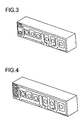
- FIG. 3 is a perspective view showing another embodiment of duplexer comprising the dielectric filter of FIG. 1;
- FIG. 4 is a perspective view showing another embodiment of duplexes comprising the dielectric filter of FIG. 1;
- FIG. 5 is a perspective view showing a conventional dielectric filter
- FIG. 6 is a graph showing the characteristics of the dielectric filter of the invention.
- FIG. 7 is a graph showing the characteristics of the conventional dielectric filter.
- FIG. 8 is a graph showing the characteristics of the conventional dielectric filter.
- the dielectric filter which is the basic device of the invention comprises a dielectric block 1 prepared from a ceramic material or the like and having hollow bores 40 , 41 , 45 , 46 , Conductive layers are formed on the outer peripheral side surface 20 of the block 1 and in the vicinity of openings of the bores in the upper surface thereof as indicated at 33 , 34 , 51 , 52 .
- a first electrode 30 and a second electrode 31 which are electrically separate from the conductive layers are formed on the upper surface.
- the bores 40 , 41 are arranged between the first and second electrodes 30 , 31 .
- the first electrode 30 is connected to an antenna (not shown), and the second electrode 31 to a receiver.
- a band-pass filter is provided by the bores 40 , 41 arranged between the first and second electrodes 30 , 31 and the conductive layers 33 , 34 in the vicinity of the openings of the bores.
- the frequencies of the desired pass band are determined by suitably adjusting the shape of the bores and the shape of the conductive layers.
- the conductive layer 38 is capacitance-coupled to the bores 40 , 41 to adjust the frequencies of the pass band.
- the bores 45 , 46 between the second electrode 31 and the conductive layer on the peripheral side surface 20 provide a trap for the second electrode, near frequencies of the pass band.
- the near-by frequency is determined by suitably adjusting the shape of the bores and the shape of the conductive layers.
- the bores 45 , 46 between the second electrode 31 and the conductive layer on the peripheral side surface 20 are arranged perpendicular to the direction of arrangement of the bores 40 , 41 between the first and second electrodes 30 , 31 .
- FIG. 6 The characteristics of the dielectric filter of FIG. 1 are shown in FIG. 6.
- two poles can be formed in the higher suppression band outside the pass band as shown in FIG. 6 by providing the plurality of bores 45 , 46 between the second electrode 31 and the conductive layer on the outer peripheral side surface.
- FIGS. 7 and 8 With reference to the prior art shown in FIGS. 7 and 8, when the characteristics required involve an attenuation of at least a (dB) at a frequency f 3 and an attenuation of at least b (dB) at a frequency f 4 , there arises a need for a trap providing a great attenuation of c (dB) near the frequency f 3 to cause an undesirable attenuation at the portion d of the pass band.
- the present embodiment has two attenuation poles such that a trap of a1 (dB) slightly greater than the attenuation a (dB) is provided near the frequency f 3 , and a trap of b1 slightly grater than the attenuation b (dB) is provided at f 4 to thereby minimize the attenuation (indicated at d in FIG. 7) due to the influence of trap in the pass band.
- the bores 45 , 46 between the second electrode 31 and the conductive layer on the peripheral side surface 20 are arranged perpendicular to the direction of arrangement of the bores 40 , 41 between the first and second electrodes 30 , 31 , so that these bores can be provided without increasing the size of the filter.
- FIG. 2 shows a dielectric duplexer which comprises two dielectric filters of FIG. 1.
- a plurality of hollow bores 40 , 41 are arranged between a first electrode 30 and a second electrode 31 .
- a plurality of hollow bores 45 , 46 are arranged between the second electrode 31 and an outer peripheral side surface.
- a plurality of hollow bores 42 to 44 are arranged between the first electrode 30 and a third electrode 32
- a plurality of hollow bores 47 , 48 are arranged between the third electrode 32 and the outer peripheral side surface 20 .
- the first electrode 30 is connected to an antenna (not shown), the second electrode 31 to a transmitter, and the third electrode 32 to a receiver.
- a band-pass filter of the desired transmission frequency band is provided by suitably adjusting the dimensions and shapes (e.g., the diameter and depth of bores, and distance between conductive layers) of the bores 40 , 41 between the first and second electrodes 30 , 31 and the conductive layers 33 , 34 in the vicinity of openings of these bores and thereby providing capacitance-coupled resonators.
- Traps having attenuation poles at two desired frequencies in the vicinity of the above-mentioned transmission frequency band can be provided by suitably adjusting the shapes of the bores 45 , 46 between the second electrode 31 and the conductive layer on the peripheral side surface 20 and the conductive layers 51 , 52 in the vicinity of openings of the bores.
- a predetermined band-pass filter for the receiving frequency band is provided by suitably adjusting the dimensions and shapes of the bores 42 to 44 between the first and third electrodes 30 , 32 and the conductive layers 35 to 37 in the vicinity of openings of these bores.
- Traps having two attenuation poles in the vicinity of the receiving frequency band can be provided by suitably adjusting the shapes of the bores 47 , 48 between the third electrode 32 and the conductive layer on the outer side surface and the conductive layers 53 , 54 in the vicinity of openings of the bores.
- the attenuation in the transmission and receiving pass bands can be minimized.
Landscapes
- Physics & Mathematics (AREA)
- Electromagnetism (AREA)
- Control Of Motors That Do Not Use Commutators (AREA)
Abstract
Description
- The present invention relates to dielectric filter devices for determining the frequency band pass characteristics to be used in mobile communications devices or the like.
- It is generally known that monoblock-type dielectric filters are used in mobile communications devices for transmitting and receiving signals, for example, in the frequency band of hundreds of megahertz to several gigahertz. Mobile communications devices, such as portable telephones, in recent years are adapted to serve a multiplicity of functions and made more compact and lightweight, and many monoblock-type dielectric duplexers are singly adapted to process different transmission and receiving frequencies for use in such devices (for example, Japanese Patent No. 3205337).
- An example of duplexer which is such a conventional dielectric filter of the monoblock type will be described with reference to FIG. 5. A
dielectric block 10, for example, of a ceramic material or the like hashollow bores 40 to 44, 49, 50. Electrically conductive layers are formed on the outerperipheral side surface 20 of the block and the upper surface thereof around the openings of the bores as indicated at 33 to 39. Further provided on the upper surface are afirst electrode 30,second electrode 31 andthird electrode 32 which are separate from these conductive layers. - As shown in FIG. 5, the
bores first electrode 30 and thesecond electrode 31. Thebore 49 is positioned between thesecond electrode 31 and the peripheral side surface. Thebores 42 to 44 are arranged between thefirst electrode 30 and thethird electrode 32. Thebore 50 is positioned between thethird electrode 32 and theperipheral side surface 20. Thefirst electrode 30 is connected to an antenna (not shown), thesecond electrode 31 to a transmitter, and thethird electrode 32 to a receiver. - A band-pass filter for the desired transmission frequency band is provided by suitably adjusting the dimensions and shapes (e.g., the diameter and depth of bores, and distance between conductive layers) of the
bores second electrodes conductive layers bore 49 between thesecond electrode 31 and the conductive layer on theperipheral side surface 20 and theconductive layer 38 in the vicinity of opening of the bore - Similarly, a predetermined band-pass filter for the receiving frequency band is provided by suitably adjusting the dimensions and shapes of the
bores 42 to 44 between the first andthird electrodes conductive layers 35 to 37 in the vicinity of openings of these bores. A trap having an attenuation pole in the vicinity of the receiving frequency band can be provided by suitably adjusting the shapes of thebore 50 between thethird electrode 32 and the conductive layer on the peripheral side surface and theconductive layer 39 in the vicinity of opening of the bore. - The dielectric duplexer described comprises two dielectric filters having two systems, i.e., transmitting system and receiving system, which use different frequencies. Since the filters are based on the same principles of the band-pass function and the trap function, these functions will be described with respect to the receiving system with reference to the filter characteristics diagrams of FIGS. 7 and 8.
- FIG. 8 shows the characteristics of the band-pass filter which is capacitance-coupled by the bores provided between the first electrode and the third electrode and the conductive layers in the vicinity of these bores. The shapes of these bores and the conductive layers in the vicinity of the openings thereof are so adjusted as to provide the desired frequency pass band f 1 to f2. Ideally, it is desirable that the attenuation be as great as possible in the suppressing band outside the pass band, whereas in actuality, a sharp attenuation is not available at a frequency in the suppressing band near the pass band.
- In communications devices, however, it is likely that a frequency near the pass band will also be used, for example, for processing signals in the receiver provided subsequent to the filter. In such a case, the receiving filter needs to have such attenuation characteristics that in the range of from the frequency f 2 at the pass-band limit to a frequency f4 which is used for other signal transmission or receiving, the attenuation is at least a (dB) for example at a frequency of f3 and at least b (dB) at the frequency f4. With reference to FIG. 8, the attenuation of the receiving filter is smaller than b (dB) at the frequency f4 for other use, and there arises the problem that a sufficiently great S/N ratio is not available.
- Accordingly with the conventional filter shown in FIG. 5, the
bore 50 between thethird electrode 32 and the conductive layer on the peripheral side surface and theconductive layer 39 near the opening of the bore are suitably adjusted in shape to thereby provide a trap having an attenuation pole, i.e., a great attenuation of c (dB), for example, in the vicinity of the frequency f3, and an attenuation of b (dB) also at a frequency over the frequency f4 shown in FIG. 7. - This method nevertheless requires an increased attenuation at f 3, such that an attenuation occurs also near the frequency f2 within the required pass band as indicated at d. The same is also true of the transmission side including the first and
second electrodes - In the field of mobile communications devices such as portable telephones, it is required in recent years that the parts be made ever smaller. Since mobile phones need to be highly portable as an important feature of the commercial product and must therefore be smaller in size, it is not desirable to provide improved filter characteristics by adding anew circuit components to the dielectric filter described.
- To overcome the foregoing problems, the present invention provides a dielectric filter device comprising a dielectric block generally in the form of a rectangular parallelepiped and having a plurality of hollow bores formed therein and openings of the bores in an upper surface of the block, electrically conductive layers respectively covering a lower surface opposed to the upper surface, an outer peripheral side surface parallel to axes of the bores, inner peripheral surfaces defining the respective bores and the upper surface around the bore openings, and a plurality of electrodes separate from the conductive layers for connection to external devices. First bore opening portions are arranged between the first electrode formed on the upper surface or side surface of the block and the second electrode formed on the upper surface thereof to provide a filter for passing a predetermined frequency band, second bore opening portions being arranged between the second electrode and the side surface of the block.
- In the dielectric filter device described, the second bore opening portions are preferably arranged perpendicular to the direction of arrangement of the first bore opening portions.
- The invention described gives improved characteristics to the dielectric filter without providing external components on the filter.
- FIG. 1 is a perspective view showing a dielectric filter of the present invention;
- FIG. 2 is a perspective view showing a duplexer comprising the dielectric filter of FIG. 1;
- FIG. 3 is a perspective view showing another embodiment of duplexer comprising the dielectric filter of FIG. 1;
- FIG. 4 is a perspective view showing another embodiment of duplexes comprising the dielectric filter of FIG. 1;
- FIG. 5 is a perspective view showing a conventional dielectric filter;
- FIG. 6 is a graph showing the characteristics of the dielectric filter of the invention;
- FIG. 7 is a graph showing the characteristics of the conventional dielectric filter; and
- FIG. 8 is a graph showing the characteristics of the conventional dielectric filter.
- Embodiments of the present invention will be described below with reference to FIGS. 1 to 4. The dielectric filter which is the basic device of the invention comprises a dielectric block 1 prepared from a ceramic material or the like and having
hollow bores peripheral side surface 20 of the block 1 and in the vicinity of openings of the bores in the upper surface thereof as indicated at 33, 34, 51, 52. Afirst electrode 30 and asecond electrode 31 which are electrically separate from the conductive layers are formed on the upper surface. - The
bores second electrodes second electrode 31 and the peripheral side surface arehollow bores bores second electrodes - The
first electrode 30 is connected to an antenna (not shown), and thesecond electrode 31 to a receiver. A band-pass filter is provided by thebores second electrodes conductive layers conductive layer 38 is capacitance-coupled to thebores bores second electrode 31 and the conductive layer on theperipheral side surface 20 provide a trap for the second electrode, near frequencies of the pass band. The near-by frequency is determined by suitably adjusting the shape of the bores and the shape of the conductive layers. - More preferably, the
bores second electrode 31 and the conductive layer on theperipheral side surface 20 are arranged perpendicular to the direction of arrangement of thebores second electrodes - The characteristics of the dielectric filter of FIG. 1 are shown in FIG. 6. According to this embodiment, two poles can be formed in the higher suppression band outside the pass band as shown in FIG. 6 by providing the plurality of
bores second electrode 31 and the conductive layer on the outer peripheral side surface. With reference to the prior art shown in FIGS. 7 and 8, when the characteristics required involve an attenuation of at least a (dB) at a frequency f3 and an attenuation of at least b (dB) at a frequency f4, there arises a need for a trap providing a great attenuation of c (dB) near the frequency f3 to cause an undesirable attenuation at the portion d of the pass band. - However the present embodiment has two attenuation poles such that a trap of a1 (dB) slightly greater than the attenuation a (dB) is provided near the frequency f 3, and a trap of b1 slightly grater than the attenuation b (dB) is provided at f4 to thereby minimize the attenuation (indicated at d in FIG. 7) due to the influence of trap in the pass band.
- Furthermore, the
bores second electrode 31 and the conductive layer on theperipheral side surface 20 are arranged perpendicular to the direction of arrangement of thebores second electrodes - FIG. 2 shows a dielectric duplexer which comprises two dielectric filters of FIG. 1. A plurality of
hollow bores first electrode 30 and asecond electrode 31. A plurality ofhollow bores second electrode 31 and an outer peripheral side surface. Further a plurality ofhollow bores 42 to 44 are arranged between thefirst electrode 30 and athird electrode 32, and a plurality ofhollow bores third electrode 32 and the outerperipheral side surface 20. - For example, the
first electrode 30 is connected to an antenna (not shown), thesecond electrode 31 to a transmitter, and thethird electrode 32 to a receiver. A band-pass filter of the desired transmission frequency band is provided by suitably adjusting the dimensions and shapes (e.g., the diameter and depth of bores, and distance between conductive layers) of thebores second electrodes conductive layers bores second electrode 31 and the conductive layer on theperipheral side surface 20 and theconductive layers - Similarly, a predetermined band-pass filter for the receiving frequency band is provided by suitably adjusting the dimensions and shapes of the
bores 42 to 44 between the first andthird electrodes conductive layers 35 to 37 in the vicinity of openings of these bores. Traps having two attenuation poles in the vicinity of the receiving frequency band can be provided by suitably adjusting the shapes of thebores third electrode 32 and the conductive layer on the outer side surface and theconductive layers - The device of the present invention is not limited to the foregoing embodiments in construction but can be modified variously within the technical scope defined in the appended claims.
Claims (4)
Applications Claiming Priority (2)
| Application Number | Priority Date | Filing Date | Title |
|---|---|---|---|
| JP2002-121363 | 2002-04-23 | ||
| JP2002121363A JP2003318606A (en) | 2002-04-23 | 2002-04-23 | Dielectric filter |
Publications (2)
| Publication Number | Publication Date |
|---|---|
| US20030197580A1 true US20030197580A1 (en) | 2003-10-23 |
| US6696905B2 US6696905B2 (en) | 2004-02-24 |
Family
ID=29208047
Family Applications (1)
| Application Number | Title | Priority Date | Filing Date |
|---|---|---|---|
| US10/230,397 Expired - Fee Related US6696905B2 (en) | 2002-04-23 | 2002-08-29 | Dielectric filter device having perpendicular bores for improved pass band characteristics |
Country Status (3)
| Country | Link |
|---|---|
| US (1) | US6696905B2 (en) |
| JP (1) | JP2003318606A (en) |
| CN (1) | CN1284264C (en) |
Cited By (2)
| Publication number | Priority date | Publication date | Assignee | Title |
|---|---|---|---|---|
| USD805475S1 (en) * | 2016-12-20 | 2017-12-19 | Cirocomm Technology Corp. | Dielectric filter |
| WO2018057722A1 (en) * | 2016-09-23 | 2018-03-29 | Cts Corporation | Ceramic rf filter with structure for blocking rf signal coupling |
Families Citing this family (3)
| Publication number | Priority date | Publication date | Assignee | Title |
|---|---|---|---|---|
| JP2004023188A (en) * | 2002-06-12 | 2004-01-22 | Sanyo Electric Co Ltd | Dielectric duplexer |
| US7545240B2 (en) * | 2005-05-24 | 2009-06-09 | Cts Corporation | Filter with multiple shunt zeros |
| KR101007935B1 (en) * | 2009-03-16 | 2011-01-14 | 서강대학교산학협력단 | Integral dielectric multiplexer capable of multiband processing |
Family Cites Families (2)
| Publication number | Priority date | Publication date | Assignee | Title |
|---|---|---|---|---|
| CA2114029C (en) | 1992-05-26 | 1997-11-18 | Darioush Agahi-Kesheh | Multi-passband dielectric filter construction |
| JPH08330808A (en) * | 1995-05-29 | 1996-12-13 | Ngk Spark Plug Co Ltd | Dielectric filter |
-
2002
- 2002-04-23 JP JP2002121363A patent/JP2003318606A/en active Pending
- 2002-08-29 US US10/230,397 patent/US6696905B2/en not_active Expired - Fee Related
-
2003
- 2003-04-23 CN CNB031240402A patent/CN1284264C/en not_active Expired - Fee Related
Cited By (3)
| Publication number | Priority date | Publication date | Assignee | Title |
|---|---|---|---|---|
| WO2018057722A1 (en) * | 2016-09-23 | 2018-03-29 | Cts Corporation | Ceramic rf filter with structure for blocking rf signal coupling |
| US10333191B2 (en) | 2016-09-23 | 2019-06-25 | Cts Corporation | Ceramic block RF filter having a first plurality of through-hole resonators and a second plurality of through-holes for blocking RF signal coupling |
| USD805475S1 (en) * | 2016-12-20 | 2017-12-19 | Cirocomm Technology Corp. | Dielectric filter |
Also Published As
| Publication number | Publication date |
|---|---|
| JP2003318606A (en) | 2003-11-07 |
| CN1453899A (en) | 2003-11-05 |
| US6696905B2 (en) | 2004-02-24 |
| CN1284264C (en) | 2006-11-08 |
Similar Documents
| Publication | Publication Date | Title |
|---|---|---|
| US6326866B1 (en) | Bandpass filter, duplexer, high-frequency module and communications device | |
| JP2004023567A (en) | Mounting structure for dielectric filter, dielectric filter device, and mounting structure for dielectric duplexer and communication equipment system | |
| US5731746A (en) | Multi-frequency ceramic block filter with resonators in different planes | |
| JP3473489B2 (en) | Dielectric filter, dielectric duplexer and communication device | |
| US6677836B2 (en) | Dielectric filter device having conductive strip removed for improved filter characteristics | |
| JPH11186819A (en) | Band rejection filter and duplexer | |
| US6696905B2 (en) | Dielectric filter device having perpendicular bores for improved pass band characteristics | |
| US7541893B2 (en) | Ceramic RF filter and duplexer having improved third harmonic response | |
| JPH0234001A (en) | Band stop filter | |
| US6747527B2 (en) | Dielectric duplexer and communication apparatus | |
| US20060164182A1 (en) | Surface acoustic wave filter | |
| JP3468093B2 (en) | Dielectric filter, duplexer and electronic equipment | |
| US6867663B2 (en) | Dielectric duplexer | |
| US6977565B2 (en) | Dielectric filter | |
| US6404306B1 (en) | Dielectric ceramic filter with improved electrical characteristics in high side of filter passband | |
| US6362705B1 (en) | Dielectric filter unit, duplexer, and communication apparatus | |
| KR100456004B1 (en) | Transmission band pass filter of duplexer | |
| JP3839339B2 (en) | Dielectric electronic component such as dielectric filter or dielectric duplexer, and method for adjusting attenuation characteristic of dielectric electronic component | |
| KR100419237B1 (en) | Frequency isolating circuit of a duplexer | |
| KR100733899B1 (en) | Enhanced Duplexer and Filter | |
| JP2002204106A (en) | Composite dielectric filter device and communication device | |
| US6480701B1 (en) | Composite filter, duplexer and communication apparatus | |
| KR100340405B1 (en) | A duplexer dielectric filter | |
| KR100311809B1 (en) | A dielectric filter | |
| KR100305577B1 (en) | Method for manufacturing dielectric duplexer |
Legal Events
| Date | Code | Title | Description |
|---|---|---|---|
| AS | Assignment |
Owner name: SANYO ELECTRIC CO., LTD., JAPAN Free format text: ASSIGNMENT OF ASSIGNORS INTEREST;ASSIGNORS:UMEDA, KATSUMI;UCHIYAMA, TAKAAKI;EZAKI, KENICHI;REEL/FRAME:013498/0086 Effective date: 20020820 |
|
| AS | Assignment |
Owner name: SANYO ELECTRIC CO., LTD., JAPAN Free format text: CORRECTIVE DOCUMENT REEL 013498 FRAME 0086;ASSIGNORS:UMEDA, KATSUMI;UCHIYAMA, TAKAAKI;EZAKI, KENICHI;REEL/FRAME:014000/0432 Effective date: 20020820 Owner name: SANYO ELECTRONIC COMPONENTS CO., LTD., JAPAN Free format text: CORRECTIVE DOCUMENT REEL 013498 FRAME 0086;ASSIGNORS:UMEDA, KATSUMI;UCHIYAMA, TAKAAKI;EZAKI, KENICHI;REEL/FRAME:014000/0432 Effective date: 20020820 |
|
| FEPP | Fee payment procedure |
Free format text: PAYOR NUMBER ASSIGNED (ORIGINAL EVENT CODE: ASPN); ENTITY STATUS OF PATENT OWNER: LARGE ENTITY |
|
| FPAY | Fee payment |
Year of fee payment: 4 |
|
| REMI | Maintenance fee reminder mailed | ||
| LAPS | Lapse for failure to pay maintenance fees | ||
| STCH | Information on status: patent discontinuation |
Free format text: PATENT EXPIRED DUE TO NONPAYMENT OF MAINTENANCE FEES UNDER 37 CFR 1.362 |
|
| FP | Lapsed due to failure to pay maintenance fee |
Effective date: 20120224 |