US20030196048A1 - Share masks and alias for directory coherency - Google Patents
Share masks and alias for directory coherency Download PDFInfo
- Publication number
- US20030196048A1 US20030196048A1 US10/437,863 US43786303A US2003196048A1 US 20030196048 A1 US20030196048 A1 US 20030196048A1 US 43786303 A US43786303 A US 43786303A US 2003196048 A1 US2003196048 A1 US 2003196048A1
- Authority
- US
- United States
- Prior art keywords
- processing elements
- bits
- memory
- signature
- alias
- Prior art date
- Legal status (The legal status is an assumption and is not a legal conclusion. Google has not performed a legal analysis and makes no representation as to the accuracy of the status listed.)
- Granted
Links
Images


Classifications
-
- G—PHYSICS
- G06—COMPUTING OR CALCULATING; COUNTING
- G06F—ELECTRIC DIGITAL DATA PROCESSING
- G06F12/00—Accessing, addressing or allocating within memory systems or architectures
- G06F12/02—Addressing or allocation; Relocation
- G06F12/08—Addressing or allocation; Relocation in hierarchically structured memory systems, e.g. virtual memory systems
- G06F12/0802—Addressing of a memory level in which the access to the desired data or data block requires associative addressing means, e.g. caches
- G06F12/0806—Multiuser, multiprocessor or multiprocessing cache systems
- G06F12/0815—Cache consistency protocols
- G06F12/0817—Cache consistency protocols using directory methods
- G06F12/0826—Limited pointers directories; State-only directories without pointers
-
- G—PHYSICS
- G06—COMPUTING OR CALCULATING; COUNTING
- G06F—ELECTRIC DIGITAL DATA PROCESSING
- G06F12/00—Accessing, addressing or allocating within memory systems or architectures
- G06F12/02—Addressing or allocation; Relocation
- G06F12/08—Addressing or allocation; Relocation in hierarchically structured memory systems, e.g. virtual memory systems
- G06F12/10—Address translation
- G06F12/1027—Address translation using associative or pseudo-associative address translation means, e.g. translation look-aside buffer [TLB]
- G06F12/1045—Address translation using associative or pseudo-associative address translation means, e.g. translation look-aside buffer [TLB] associated with a data cache
Definitions
- the invention relates to computer processors and memory systems. More particularly, the invention relates to optimizing coherent memory access operations within multiprocessor computer systems having distributed shared memory architectures.
- Multiprocessor, or parallel processing, computer systems rely on a plurality of microprocessors to handle computing tasks in parallel to reduce overall execution time.
- One common implementation of a multiprocessor system is the “single bus architecture, in which a plurality of processors are interconnected through a single bus.
- a networked multiprocessor systems have also been developed, which utilize processors or groups of processors connected to one another across an interconnection fabric, e.g., a network, and communicating via “packets” or messages.
- FIG. 1 shows an exemplary networked multiprocessor system 100 , in which a plurality of nodes 102 are interconnected to each other via the interconnection fabric 101 , e.g., a network.
- the interconnection fabric 101 e.g., a network.
- the networked multiprocessor system 100 may have any number of nodes.
- FIG. 1 shows an exemplary networked multiprocessor system 100 , in which a plurality of nodes 102 are interconnected to each other via the interconnection fabric 101 , e.g., a network.
- the networked multiprocessor system 100 may have any number of nodes.
- the interconnection fabric 101 is shown to provide interconnections only between the nodes 102 , all system entities, including the cells 103 , the processors 105 and the memories 104 , are interconnected, and communicate, with the rest of the system through the interconnection fabric 101 .
- Each of the nodes 102 of the networked multiprocessor system 100 may be further divided into a smaller hierarchical units—referred herein as “cells” 103 —, which comprises a plurality of processors 105 and a shared memory 104 .
- Each processor 105 may comprise any processing elements that may share data within the distributed shared memory in the system, e.g., a microprocessor, an I/O device or the like.
- the grouping into nodes and/or cells of the system entities may be made physically and/or logically.
- Each of the shared memory 104 may comprise a portion of the shared memory for the system 100 , and may include a memory controller (not shown) and/or a coherency controller (not shown) to control memory accesses thereto from various processors in the system, and to monitor the status of local copies of the memory stored in caches of various processors in the system.
- Prior attempts to address the above coherency problem is to broadcast an “invalidate” signal, whenever the shared memory location is updated, to every entity, e.g., processors 105 , in the system 100 that may potentially share the memory location so that each of the entity may “invalidate” the copy in its cache, and the data would be obtained from the memory rather than the entity's cache in a subsequent access.
- an address aliasing error e.g., error during a translation from physical address to a virtual address
- a duplicate copy of a cache line addresses of the copies being different from each other. This may disturb the data coherency of the system, and eventually cause data corruptions, which often result in a fatal system crash.
- a method of data sharing in a distributed computing system having a plurality of processing elements and at least one memory having stored therein a plurality of cache lines comprises providing a plurality of shared masks, each of the plurality shared masks corresponding to an associated one of the plurality of cache lines in the at least one memory, and each of the plurality of shared masks having a plurality of bits, each of the plurality of bits indicating whether at least one of the plurality of processing elements may be sharing the associated one of the plurality of cache lines, and wherein the number of the plurality of bits is less than the number of the plurality of processing elements.
- an apparatus for data sharing in a distributed computing system having a plurality of processing elements and at least one memory having stored therein a plurality of cache lines comprises a plurality of shared masks, each of the plurality shared masks corresponding to an associated one of the plurality of cache lines in the at least one memory, and each of the plurality of shared masks having a plurality of bits, each of the plurality of bits being associated with one or more of the plurality of processing elements, and each of the plurality of bits indicating whether respective associated one or more of the plurality of processing elements may have a copy of the associated one of the plurality of cache lines, and wherein a number of the plurality of bits is less than a number of the plurality of processing elements.
- a method of detecting an address aliasing error in a computing system having at least one memory having stored therein at least one cache line comprises providing a directory tag alias signature for each of the at least one cache line, the directory tag alias signature having encoded therein a signature of an address information of the at least one cache line, detecting a request to access the at least one cache line, the request including a requested address information of the at least one cache line, computing a computed alias signature based on the requested address information, comparing the directory tag alias signature with the computed alias signature to determine if the directory tag alias signature and the computed alias signature match each other, and indicating an occurrence of the address aliasing error if the directory tag alias signature and the computed alias signature do not match each other.
- FIG. 1 is a block diagram of the relevant portions of an exemplary conventional networked multiprocessor distributed memory system
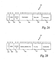
- FIG. 2A is an illustrative table showing relevant portions of an exemplary embodiment of the directory tag bits of a cache line, for the case in which the cache line is idle, in accordance with the principles of the embodiment of the present invention
- FIG. 2B is an illustrative table showing relevant portions of an exemplary embodiment of the directory tag bits of a cache line, for the case in which the cache line is being shared, in accordance with the principles of the embodiment of the present invention
- FIG. 3A shows an exemplary embodiment of a mechanism for obtaining a relative cell identification number in accordance with an aspect of the principles of the present invention
- FIG. 3B shows an example illustrating the operations of the mechanism for obtaining a relative cell identification number shown in FIG. 3A;
- FIG. 4 shows an illustrative example of the various formats in which the share mask may be encoded in accordance with an embodiment of the present invention
- FIG. 5 shows an illustrative example of the partition mask in accordance with an embodiment of the present invention
- FIG. 6 is flow diagram illustrative of an exemplary embodiment of the alias error detection process in accordance with an embodiment of the principles of the present invention.
- a directory tag for each cache line in a memory within a multiprocessor distributed memory system includes a share mask and an alias signature.
- the share mask is used to keep track of entities of the system that share the cache line, and is encoded into a fixed length field having a number of bits that is significantly less than the number of the entities.
- the share mask is utilized for maintaining coherency among shared data in the system.
- the share mask is used to identify each entity or a group of entities that share the particular location, and an invalidate message is sent to each of the identified entity or group of entities, eliminating the need to broadcast the message to all entities in the system, and thus conserving the communication bandwidth of the system.
- the alias signature in the directory tag is compared with an alias signature computed from the memory access request to prevent data corruptions that may occur due to address aliasing errors.
- directory tag bits are provided for each cache line stored in a memory of the networked multiprocessor distributed memory system (e.g., shown in FIG. 1), an exemplary embodiment of which is shown in FIGS. 2A and 2B.
- the directory tag bits 201 comprise 27 bits, TAG [26:0], arranged as a number of fields, including: an one bit Idle field (I) 203 (TAG [26]), a two bits miscellaneous field (MISC) 204 (TAG [25:24]), a two bits state field (STATE) 205 (TAG [23:22]), an eight bits share mask field (SHARE_MASK) 206 (TAG [21:14]), an eight bit virtual index field (VI) 207 (TAG [13:6]) and a six bits alias signature field (ALIAS) 208 (TAG [5:0]).
- I Idle field
- MISC miscellaneous field
- STATE two bits state field
- SHARE_MASK eight bits share mask field
- VI virtual index field
- ALIAS alias signature field
- the MISC field contains miscellaneous information associated with the cache line, e.g., for performing housekeeping operations.
- the idle field (I) 203 , the state field (STATE) 205 and the highest bit of the virtual index (VI [7]) field 207 are used to encode the relevant state of the cache line as shown in table 1: TABLE 1 I, STATE [1:0], VI [7] State 1xxx or IDLE 0000 0001 I/O PRIVATE 001x CPU PRIVATE 010x INTRA-NODAL SHARED (2 cells/bit) 011x INTER-NODAL SHARED (8 cells/bit)
- a cache line is in the “idle” state, the cache line is owned exclusively by the memory, and thus is not shared by any system entity.
- the states “CPU PRIVATE” and “ 1 / 0 PRIVATE” each indicate that the cache line is exclusively owned by a processor or an I/O device, respectively.
- the state “INTRA-NODAL SHARED” indicates that the cache line is shared by cells 103 that are located within the same node 102 in which the particular shared memory 104 is located.
- the state “INTER-NODAL SHARED” indicates that the cache line maybe shared by cells 103 that are located outside the node 102 in which the particular shared memory 104 is located.
- a node 102 may include any number of cells 103
- a cell 103 may comprise any number of processors 105 .
- a cell 103 comprises four (4) processors 105 and at least one memory 104
- a node 102 comprises sixteen (16) cells 103
- a memory 104 comprises a memory controller and a coherency controller to control the data traffic to and from the memory 104 , and to control coherency operations, respectively.
- a memory 104 has stored therein the above described directory tag bits for each cache line.
- Every processors 105 and the memory 104 within a single cell 103 share a unique cell ID.
- the cells 103 are connected through an interconnect mechanism which has non-uniform latency and bandwidth characteristics.
- the interconnect mechanism is such that cells which are physically located close together have a lower-latency, higher bandwidth connection than cells that are physically far apart.
- the cell IDs are chosen so that cells which are physically close to each other also have only the LSBs of their cell IDs different, i.e., cells 4 and 5 are physically close whereas cells 1 and 16 are physically far apart.
- a relative cell ID is constructed by exclusive-ORing together the cell ID of the memory 104 with the cell ID of a potential sharer of a cache line in the memory 104 .
- the memory 104 is in cell number 3, i.e., the cell ID of the memory 104 is 3 (0000011)
- a sharer is in the cell number 30 (0011110), e.g., the sharer is a processor 105 located in cell number 30, then the resulting relative cell ID for the sharer relative to the particular memory in cell number 3 would be 29 (0011101) as shown in FIG. 3B.
- sharing mask bits 208 are stored in the memory 104 , depending on whether the cache line is shared intra-nodally or inter-nodally, in one of two 8 bit vector formats 401 and 402 shown in FIG. 4.
- the format 1 401 is used when all of the entities having a shared copy of the cache line are in the same node in which the shared memory 104 is located.
- each bit of the SHARE_MASK indicates whether the cache line is shared between two cells within the node. For example, a value of one (1) in the SHARE_MASK[0] indicates that a copy of the cache line maybe stored in two cells whose relative cell IDs are 1 and 0, i.e., r_id [1:0].
- the format 2 402 is used when at least one of the entity having a shared copy of the cache line is located in a node different from the node at which the shared memory 104 is located.
- each bit of the SHARE_MASK indicates whether the cache line is shared between eight cells from any of the nodes 102 .
- a value of one (1) in the SHARE_MASK[0] indicates that a copy of the cache line may be stored in eight cells whose relative cell IDs are 0, 1, 2, 3, 4, 5, 6, and 7, i.e., r_id [7:0].
- the SHARE_MASK bits 0 through 3 i.e., SHARE_MASK [3:0]
- the SHARE_MASK bits 4 through 7 i.e., SHARE_MASK [7:4] of the format 1
- the SHARE_MASK bit 0 i.e., SHARE_MASK [0]
- the SHARE_MASK bit 1 i.e., SHARE_MASK [1]
- the format 3 is used to unify the two memory formats, format 1 and format 2 , so that the coherency controller doesn't have to store and manipulate the share mask in two different formats.
- the directory tag associated with the requested cache line is read by the coherency controller, which, based on the state information (e.g., shown in Table 1) and the SHARE_MASK of the cache line, reconstructs the share mask into a fourteen bit format 3 as shown in FIG. 4.
- the SHARE_MASK bits 0 through 7 i.e., SHARE_MASK [7:0], of format 1 and the SHARE_MASK bits 2 through 7 , i.e., SHARE_MASK [7:2], of the format 2 may be directly mapped to the SHARE_MASK bits 0 through 7 , i.e., SHARE_MASK [7:0], and the SHARE_MASK bits 8 through 13 , i.e., SHARE_MASK [13:8], of the format 3 , respectively. Conversions to and from either formats 1 or 2 and format 3 is straightforward and consumes little logic or delay time.
- the coherency controller may send invalidate messages to each entity that may have a copy of the cache line as indicated by the share mask.
- a partition of the system 100 into one or more logically separate subsystems, each of which may operate independently with respect to each other.
- each subsystem may comprise a computing system in its own right.
- the partition is sometimes also referred to as a “protection domain”.
- sharing memories across the partition may be undesirable, and thus invalidate messages should not be issued across protection domain boundaries.
- a partition mask 501 as shown in FIG. 5 is provided to be accessible to each coherency controller, and may be used to further mask the share mask to prevent any entities outside the protection domain from receiving an invalidate message.
- the partition mask 501 comprises the same number of bits as the format 3 share mask, each corresponding to the respective bits of the format 3 share mask. For example, a one (1) in the bit 0 of the partition mask indicate that cells, whose relative cell IDs are r_id [1:0], are not within the same protection domain, and thus should not receive the invalidate messages. Because the partitions are typically made by grouping closely located entities, and because the relative cell IDs are based on the proximity of the entities, the partition mask provides a convenient way in which to maintain the integrity of the protection domain boundaries.
- the partition mask may also be used to indicate physically absent cells, and thus to prevent issuing of invalidate messages to a non-existing cell.
- the coherency controller performs an AND logic operation between the respective bits of the share mask in format 3 and the partition mask to produce a further masked shared mask bits.
- the coherency controller then, traverses the further masked share mask bit by bit, preferably starting from the least significant bit (LSB). For each further masked share mask bit having a value of a one (1), the coherency controller performs a table lookup operation to determine the actual cell ID(s) corresponding to the relative cell ID(s) associated with further masked share mask bit. In this manner, the coherency controller eventually identifies all cells that may have a copy of the cache line.
- LSB least significant bit
- the coherency controller then sends an invalidate message to each of the identified cells, and when invalidate responses are received therefrom, allows the request for the cache line to proceed.
- the SHARED_MASK bits described above can be encoded as a small number of fixed length bits, can track the system entities that may share a cache line, and significantly reduces the coherency message and response traffic, enabling the system bandwidth to be conserved.
- a directory tag in addition to the SHARE_MASK bits, contains a 6 bit alias signature field, ALIAS [5:0] 208 .
- the alias signature field contains a signature of the cache line address and/or status information that may be used to detect improper address aliasing.
- a particular cache line may be allowed to be accessed by one or more different physical addresses, e.g., depending on the current operational mode.
- the high order address bits of the one or more different physical addresses are required to be different.
- only one address should be used at any given time, and any transitions between the different addresses should be allowed to happen only if the coherency state of the cache line is idle, i.e., exclusively owned by the memory.
- system software is entrusted to enforce this requirement, errors in the system software may cause the same memory location to be referenced from two different addresses.
- Another type of address aliasing could occur because the translation between a physical address and a cell address is done in several places, e.g., to optimize system performance.
- a programming and/or hardware error causes an error in one of the translations, the same memory location may referenced from two different addresses.
- an alias signature field is computed and stored in the directory tag as shown in FIG. 2B.
- the alias signature may be computed according to the following equation:
- the addr [43:36] are the high bits of the physical address of the cache line
- Ex-OR represent an exclusive ORing operation between respective bits
- ⁇ ⁇ represent a concatenation of bits enclosed therein
- 1′b0 means a single bit having the value
- 2′b00 means two bits having the value 00.
- each cell there is provided for each cell, a cell map table that contains values for the cell_addr, the intlv and, optionally, offset numbers for each entity within the cell.
- the intlv indicates, e.g., the memory interleaving policy being used by the cell.
- step 1 Whenever a new memory access request is made (step 1 ), the alias signature 208 is read from the directory tag 201 associated with the requested cache line in step 602 .
- a new alias signature is computed from the information, e.g., the address, contained in the new memory access request.
- this newly computed alias signature is compared to the alias signature read from the directory tag.
- step 605 If a determination is made, in step 605 , that the comparison resulted in a match the memory request is allowed to be processed in the normal manner in step 609 .
- step 607 If, on the other hand, the cache line state is non-idle, then a fatal error is reported to system software in step 607 .
- the normal processing of the system is halted in step 608 without processing the memory access request, and thus before occurrence of any data corruption due to loss of data coherency.
- the alias signature mechanism described herein allows detecting an address aliasing error before any corruption of data occurs.
Landscapes
- Engineering & Computer Science (AREA)
- Theoretical Computer Science (AREA)
- Physics & Mathematics (AREA)
- General Engineering & Computer Science (AREA)
- General Physics & Mathematics (AREA)
- Memory System Of A Hierarchy Structure (AREA)
Abstract
Description
- The invention relates to computer processors and memory systems. More particularly, the invention relates to optimizing coherent memory access operations within multiprocessor computer systems having distributed shared memory architectures.
- Multiprocessor, or parallel processing, computer systems rely on a plurality of microprocessors to handle computing tasks in parallel to reduce overall execution time. One common implementation of a multiprocessor system is the “single bus architecture, in which a plurality of processors are interconnected through a single bus. However, because of the limited bandwidth of the single bus also limits the number of processors that can be interconnected thereto, recently a networked multiprocessor systems have also been developed, which utilize processors or groups of processors connected to one another across an interconnection fabric, e.g., a network, and communicating via “packets” or messages.
- Typically, in a networked multiprocessor system includes a plurality of nodes or clusters interconnected via a network. For example, FIG. 1 shows an exemplary networked
multiprocessor system 100, in which a plurality ofnodes 102 are interconnected to each other via theinterconnection fabric 101, e.g., a network. By way of an example, only two nodes are shown. However, thenetworked multiprocessor system 100 may have any number of nodes. Moreover, although, in FIG. 1, theinterconnection fabric 101 is shown to provide interconnections only between thenodes 102, all system entities, including thecells 103, theprocessors 105 and thememories 104, are interconnected, and communicate, with the rest of the system through theinterconnection fabric 101. - Each of the
nodes 102 of thenetworked multiprocessor system 100 may be further divided into a smaller hierarchical units—referred herein as “cells” 103—, which comprises a plurality ofprocessors 105 and a sharedmemory 104. Eachprocessor 105 may comprise any processing elements that may share data within the distributed shared memory in the system, e.g., a microprocessor, an I/O device or the like. The grouping into nodes and/or cells of the system entities may be made physically and/or logically. - Each of the shared
memory 104 may comprise a portion of the shared memory for thesystem 100, and may include a memory controller (not shown) and/or a coherency controller (not shown) to control memory accesses thereto from various processors in the system, and to monitor the status of local copies of the memory stored in caches of various processors in the system. - In a networked multiprocessor system such as one described above, multiple copies of a piece of data from the shared memory may be stored in the caches of various processors. Each processor that has a copy of the data in its cache is said to “share” the data-the data is often referred to as one or more “cache lines”. In order to maintain a proper operation of the networked multiprocessor system, it is critical to ensure that all copies of any shared data must be identical to the data in the shared memory, e.g., a coherency between the copies and the data in the memory must be ensured.
- Prior attempts to address the above coherency problem is to broadcast an “invalidate” signal, whenever the shared memory location is updated, to every entity, e.g.,
processors 105, in thesystem 100 that may potentially share the memory location so that each of the entity may “invalidate” the copy in its cache, and the data would be obtained from the memory rather than the entity's cache in a subsequent access. - Unfortunately, however, the broadcasting of invalidate signal to all potential sharers, e.g., all
processors 105, is wasteful of the system bandwidth since as many invalidate messages as there are processors in the system must be sent, and the resulting invalidate response messages from each of the processors, across the system interconnectfabric 101 and/or the data paths connecting each processors to the system. This lowers the system performance. - Prior attempts were made to address the above waste of system bandwidth by restricting the sharing of memory to within one of the
nodes 102 at a time. This approach is inefficient and inflexible in that if a new sharer from a different node was to be added to the list of sharers, the other sharers in the list must be invalidated first before the new sharer can be added. This tend to increase the invalidate message traffic, and thus has negative system performance implications, particularly for cache lines that should preferably be shared as read-only by all processors. - Moreover, in a distributed shared memory system, an address aliasing error, e.g., error during a translation from physical address to a virtual address, may result in a duplicate copy of a cache line, addresses of the copies being different from each other. This may disturb the data coherency of the system, and eventually cause data corruptions, which often result in a fatal system crash.
- Prior attempts to address this aliasing error problem includes running a large test suit under system software and looking for signs of data corruption. Unfortunately, however, this prior solution is an after-the-fact approach that can only detect data corruption, i.e., after a data corruption has already happened.
- Thus, there is a need for more efficient method and device for providing tracking of the system entities that may share a cache line to maintain data coherency in a multiprocessor system, which avoids sending coherency messages to all entities in the multiprocessor system.
- There is also a need for more efficient method and device for detecting an address aliasing error before a corruption of data occurs.
- In accordance with the principles of the present invention, a method of data sharing in a distributed computing system having a plurality of processing elements and at least one memory having stored therein a plurality of cache lines comprises providing a plurality of shared masks, each of the plurality shared masks corresponding to an associated one of the plurality of cache lines in the at least one memory, and each of the plurality of shared masks having a plurality of bits, each of the plurality of bits indicating whether at least one of the plurality of processing elements may be sharing the associated one of the plurality of cache lines, and wherein the number of the plurality of bits is less than the number of the plurality of processing elements.
- In addition, in accordance with the principles of the present invention, an apparatus for data sharing in a distributed computing system having a plurality of processing elements and at least one memory having stored therein a plurality of cache lines comprises a plurality of shared masks, each of the plurality shared masks corresponding to an associated one of the plurality of cache lines in the at least one memory, and each of the plurality of shared masks having a plurality of bits, each of the plurality of bits being associated with one or more of the plurality of processing elements, and each of the plurality of bits indicating whether respective associated one or more of the plurality of processing elements may have a copy of the associated one of the plurality of cache lines, and wherein a number of the plurality of bits is less than a number of the plurality of processing elements.
- In accordance with another aspect of the principles of the present invention, a method of detecting an address aliasing error in a computing system having at least one memory having stored therein at least one cache line comprises providing a directory tag alias signature for each of the at least one cache line, the directory tag alias signature having encoded therein a signature of an address information of the at least one cache line, detecting a request to access the at least one cache line, the request including a requested address information of the at least one cache line, computing a computed alias signature based on the requested address information, comparing the directory tag alias signature with the computed alias signature to determine if the directory tag alias signature and the computed alias signature match each other, and indicating an occurrence of the address aliasing error if the directory tag alias signature and the computed alias signature do not match each other.
- Features and advantages of the present invention will become apparent to those skilled in the art from the following description with reference to the drawings, in which:
- FIG. 1 is a block diagram of the relevant portions of an exemplary conventional networked multiprocessor distributed memory system;
- FIG. 2A is an illustrative table showing relevant portions of an exemplary embodiment of the directory tag bits of a cache line, for the case in which the cache line is idle, in accordance with the principles of the embodiment of the present invention;
- FIG. 2B is an illustrative table showing relevant portions of an exemplary embodiment of the directory tag bits of a cache line, for the case in which the cache line is being shared, in accordance with the principles of the embodiment of the present invention;
- FIG. 3A shows an exemplary embodiment of a mechanism for obtaining a relative cell identification number in accordance with an aspect of the principles of the present invention;
- FIG. 3B shows an example illustrating the operations of the mechanism for obtaining a relative cell identification number shown in FIG. 3A;
- FIG. 4 shows an illustrative example of the various formats in which the share mask may be encoded in accordance with an embodiment of the present invention;
- FIG. 5 shows an illustrative example of the partition mask in accordance with an embodiment of the present invention;
- FIG. 6 is flow diagram illustrative of an exemplary embodiment of the alias error detection process in accordance with an embodiment of the principles of the present invention.
- For simplicity and illustrative purposes, the principles of the present invention are described by referring mainly to an exemplar embodiment thereof. However, one of ordinary skill in the art would readily recognize that the same principles are equally applicable to, and can be implemented in, a multiprocessor shared memory system having a different implementation or architecture, and that any such variation would be within such modifications that do not depart from the true spirit and scope of the present invention.
- For example, while much of the following description of the present invention makes references to multiprocessor systems, it should be appreciated that the concept of distributing tasks between processors in multiprocessor systems may also be applied to distributed computer systems which distribute tasks between different computers in a networked environment (e.g., a LAN or WAN). Further, many of the functions and problems associated with multiprocessor and distributed computer systems are quite similar and equally applicable to both types of systems. Consequently, the term “networked computer system” will be used hereinafter to describe both systems in which the nodes are implemented as individual microprocessors or groups of processors (multiprocessor systems) or as individual computers which may separately utilize one or more processors (distributed computer systems).
- Moreover, the present invention is described with reference to a particular implementation in which there are a particular number of processors for each cell, a particular number of cells per node, etc. However, it should be apparent to those having an ordinary skill that the system described herein may have any number of processors and cells, and that any such variation would be within such modifications that do not depart from the true spirit and scope of the present invention.
- In accordance with the principles of the present invention, a directory tag for each cache line in a memory within a multiprocessor distributed memory system includes a share mask and an alias signature. The share mask is used to keep track of entities of the system that share the cache line, and is encoded into a fixed length field having a number of bits that is significantly less than the number of the entities. The share mask is utilized for maintaining coherency among shared data in the system.
- Before a request to access a shared location of a memory is granted, the share mask is used to identify each entity or a group of entities that share the particular location, and an invalidate message is sent to each of the identified entity or group of entities, eliminating the need to broadcast the message to all entities in the system, and thus conserving the communication bandwidth of the system. The alias signature in the directory tag is compared with an alias signature computed from the memory access request to prevent data corruptions that may occur due to address aliasing errors.
- In particular, in accordance with the principles of the present invention, directory tag bits are provided for each cache line stored in a memory of the networked multiprocessor distributed memory system (e.g., shown in FIG. 1), an exemplary embodiment of which is shown in FIGS. 2A and 2B.
- As shown in FIGS. 2A and 2B, in an embodiment of the present invention, the
directory tag bits 201 comprise 27 bits, TAG [26:0], arranged as a number of fields, including: an one bit Idle field (I) 203 (TAG [26]), a two bits miscellaneous field (MISC) 204 (TAG [25:24]), a two bits state field (STATE) 205 (TAG [23:22]), an eight bits share mask field (SHARE_MASK) 206 (TAG [21:14]), an eight bit virtual index field (VI) 207 (TAG [13:6]) and a six bits alias signature field (ALIAS) 208 (TAG [5:0]). - The MISC field contains miscellaneous information associated with the cache line, e.g., for performing housekeeping operations. The idle field (I) 203, the state field (STATE) 205 and the highest bit of the virtual index (VI [7])
field 207 are used to encode the relevant state of the cache line as shown in table 1:TABLE 1 I, STATE [1:0], VI [7] State 1xxx or IDLE 0000 0001 I/O PRIVATE 001x CPU PRIVATE 010x INTRA-NODAL SHARED (2 cells/bit) 011x INTER-NODAL SHARED (8 cells/bit) - If a cache line is in the “idle” state, the cache line is owned exclusively by the memory, and thus is not shared by any system entity. The states “CPU PRIVATE” and “ 1/0 PRIVATE” each indicate that the cache line is exclusively owned by a processor or an I/O device, respectively.
- The state “INTRA-NODAL SHARED” indicates that the cache line is shared by
cells 103 that are located within thesame node 102 in which the particular sharedmemory 104 is located. - Finally, the state “INTER-NODAL SHARED” indicates that the cache line maybe shared by
cells 103 that are located outside thenode 102 in which the particular sharedmemory 104 is located. - As can be seen from FIG. 2A, when a cache line is “idle”, i.e., owned exclusively by the memory, the SHARE_MASK and the ALIAS fields do not have any meaning, and the contents thereof may be ignored.
- Although for the purpose of illustration only, the following description is given with reference to a specific embodiment in which a particular number of
processors 105 andcells 103 are included in each of thenodes 102 in thesystem 100, it should be understood that anode 102 may include any number ofcells 103, and that acell 103 may comprise any number ofprocessors 105. - In an embodiment of the present invention, a
cell 103 comprises four (4)processors 105 and at least onememory 104, anode 102 comprises sixteen (16)cells 103, and there are four (4)nodes 102 in the system. In addition, amemory 104 comprises a memory controller and a coherency controller to control the data traffic to and from thememory 104, and to control coherency operations, respectively. Amemory 104 has stored therein the above described directory tag bits for each cache line. - Every
processors 105 and thememory 104 within asingle cell 103 share a unique cell ID. In a preferred embodiment of the present invention, thecells 103 are connected through an interconnect mechanism which has non-uniform latency and bandwidth characteristics. The interconnect mechanism is such that cells which are physically located close together have a lower-latency, higher bandwidth connection than cells that are physically far apart. The cell IDs are chosen so that cells which are physically close to each other also have only the LSBs of their cell IDs different, i.e.,cells cells - As shown in FIGS. 3A and 3B, a relative cell ID is constructed by exclusive-ORing together the cell ID of the
memory 104 with the cell ID of a potential sharer of a cache line in thememory 104. For example, if thememory 104 is incell number 3, i.e., the cell ID of thememory 104 is 3 (0000011), and a sharer is in the cell number 30 (0011110), e.g., the sharer is aprocessor 105 located incell number 30, then the resulting relative cell ID for the sharer relative to the particular memory incell number 3 would be 29 (0011101) as shown in FIG. 3B. - According to the principles of the present invention, sharing
mask bits 208 are stored in thememory 104, depending on whether the cache line is shared intra-nodally or inter-nodally, in one of two 8 bit vector formats 401 and 402 shown in FIG. 4. Theformat 1 401 is used when all of the entities having a shared copy of the cache line are in the same node in which the sharedmemory 104 is located. In this format, each bit of the SHARE_MASK indicates whether the cache line is shared between two cells within the node. For example, a value of one (1) in the SHARE_MASK[0] indicates that a copy of the cache line maybe stored in two cells whose relative cell IDs are 1 and 0, i.e., r_id [1:0]. - The
format 2 402 is used when at least one of the entity having a shared copy of the cache line is located in a node different from the node at which the sharedmemory 104 is located. In this format, each bit of the SHARE_MASK indicates whether the cache line is shared between eight cells from any of thenodes 102. For example, a value of one (1) in the SHARE_MASK[0] indicates that a copy of the cache line may be stored in eight cells whose relative cell IDs are 0, 1, 2, 3, 4, 5, 6, and 7, i.e., r_id [7:0]. - As can be seen from FIG. 4, the
SHARE_MASK bits 0 through 3, i.e., SHARE_MASK [3:0], and theSHARE_MASK bits 4 through 7, i.e., SHARE_MASK [7:4], of theformat 1 may be directly mapped to theSHARE_MASK bit 0, i.e., SHARE_MASK [0], and theSHARE_MASK bit 1, i.e., SHARE_MASK [1], of theformat 2, respectively. - In a preferred embodiment of the present invention, the
format 3 is used to unify the two memory formats,format 1 andformat 2, so that the coherency controller doesn't have to store and manipulate the share mask in two different formats. When a request for a cache line, which requires the cache line to be idle or private, is made, the directory tag associated with the requested cache line is read by the coherency controller, which, based on the state information (e.g., shown in Table 1) and the SHARE_MASK of the cache line, reconstructs the share mask into a fourteenbit format 3 as shown in FIG. 4. As can be seen, theSHARE_MASK bits 0 through 7, i.e., SHARE_MASK [7:0], offormat 1 and theSHARE_MASK bits 2 through 7, i.e., SHARE_MASK [7:2], of theformat 2 may be directly mapped to theSHARE_MASK bits 0 through 7, i.e., SHARE_MASK [7:0], and theSHARE_MASK bits 8 through 13, i.e., SHARE_MASK [13:8], of theformat 3, respectively. Conversions to and from eitherformats format 3 is straightforward and consumes little logic or delay time. - Once the share mask is put into
format 3 as shown in FIG. 4, The coherency controller may send invalidate messages to each entity that may have a copy of the cache line as indicated by the share mask. - Optionally, in a preferred embodiment, a partition of the
system 100 into one or more logically separate subsystems, each of which may operate independently with respect to each other. For example, each subsystem may comprise a computing system in its own right. The partition is sometimes also referred to as a “protection domain”. In this embodiment, sharing memories across the partition may be undesirable, and thus invalidate messages should not be issued across protection domain boundaries. Thus, in this embodiment, apartition mask 501 as shown in FIG. 5 is provided to be accessible to each coherency controller, and may be used to further mask the share mask to prevent any entities outside the protection domain from receiving an invalidate message. - In particular, the
partition mask 501 comprises the same number of bits as theformat 3 share mask, each corresponding to the respective bits of theformat 3 share mask. For example, a one (1) in thebit 0 of the partition mask indicate that cells, whose relative cell IDs are r_id [1:0], are not within the same protection domain, and thus should not receive the invalidate messages. Because the partitions are typically made by grouping closely located entities, and because the relative cell IDs are based on the proximity of the entities, the partition mask provides a convenient way in which to maintain the integrity of the protection domain boundaries. - Additionally, the partition mask may also be used to indicate physically absent cells, and thus to prevent issuing of invalidate messages to a non-existing cell.
- In operation, the coherency controller performs an AND logic operation between the respective bits of the share mask in
format 3 and the partition mask to produce a further masked shared mask bits. The coherency controller, then, traverses the further masked share mask bit by bit, preferably starting from the least significant bit (LSB). For each further masked share mask bit having a value of a one (1), the coherency controller performs a table lookup operation to determine the actual cell ID(s) corresponding to the relative cell ID(s) associated with further masked share mask bit. In this manner, the coherency controller eventually identifies all cells that may have a copy of the cache line. - The coherency controller then sends an invalidate message to each of the identified cells, and when invalidate responses are received therefrom, allows the request for the cache line to proceed.
- As can be appreciated, the SHARED_MASK bits described above can be encoded as a small number of fixed length bits, can track the system entities that may share a cache line, and significantly reduces the coherency message and response traffic, enabling the system bandwidth to be conserved.
- In accordance with another aspect of the present invention, in addition to the SHARE_MASK bits, a directory tag (shown in FIG. 2B) contains a 6 bit alias signature field, ALIAS [5:0] 208. The alias signature field contains a signature of the cache line address and/or status information that may be used to detect improper address aliasing.
- In some systems, a particular cache line may be allowed to be accessed by one or more different physical addresses, e.g., depending on the current operational mode. In these systems, the high order address bits of the one or more different physical addresses are required to be different. In order to maintain data coherency in the system, only one address should be used at any given time, and any transitions between the different addresses should be allowed to happen only if the coherency state of the cache line is idle, i.e., exclusively owned by the memory. However, since system software is entrusted to enforce this requirement, errors in the system software may cause the same memory location to be referenced from two different addresses.
- Another type of address aliasing could occur because the translation between a physical address and a cell address is done in several places, e.g., to optimize system performance. When a programming and/or hardware error causes an error in one of the translations, the same memory location may referenced from two different addresses.
- To detect those and other possible address aliasing errors, an alias signature field is computed and stored in the directory tag as shown in FIG. 2B. In an embodiment of the present invention, the alias signature may be computed according to the following equation:
- alias=cell — addr[5:0]Ex-OR{intlv[2:0], cell — addr[7:6], 1′b0}EX-OR{2′b00, addr[43:40]Ex — OR addr[39:36]};
- where the cell_addr[7:0] and the intlv [2:0] are used to compute cell address, the addr [43:36] are the high bits of the physical address of the cache line, Ex-OR represent an exclusive ORing operation between respective bits, { } represent a concatenation of bits enclosed therein, 1′b0 means a single bit having the
value - In an embodiment of the present invention, there is provided for each cell, a cell map table that contains values for the cell_addr, the intlv and, optionally, offset numbers for each entity within the cell. The intlv indicates, e.g., the memory interleaving policy being used by the cell.
- The inventive aliasing error detection process according to the principles of the present invention will now be described with references to FIG. 6.
- Whenever a new memory access request is made (step 1), the
alias signature 208 is read from thedirectory tag 201 associated with the requested cache line instep 602. A new alias signature is computed from the information, e.g., the address, contained in the new memory access request. Instep 603, this newly computed alias signature is compared to the alias signature read from the directory tag. - If a determination is made, in
step 605, that the comparison resulted in a match the memory request is allowed to be processed in the normal manner instep 609. - If, on the other hand, the comparison resulted in the two alias signatures not matching, a determination is made whether the cache line is in an “idle” state, e.g., from table 1. If the cache line is in an idle state, then the memory request is allowed to proceed in
step 609 since there is no coherency concern. - If, on the other hand, the cache line state is non-idle, then a fatal error is reported to system software in
step 607. The normal processing of the system is halted instep 608 without processing the memory access request, and thus before occurrence of any data corruption due to loss of data coherency. - As can be appreciated, the alias signature mechanism described herein allows detecting an address aliasing error before any corruption of data occurs.
- While the invention has been described with reference to the exemplary embodiments thereof, those skilled in the art will be able to make various modifications to the described embodiments of the invention without departing from the true spirit and scope of the invention. The terms and descriptions used herein are set forth by way of illustration only and are not meant as limitations. In particular, although the method of the present invention has been described by examples, the steps of the method may be performed in a different order than illustrated or simultaneously. Those skilled in the art will recognize that these and other variations are possible within the spirit and scope of the invention as defined in the following claims and their equivalents.
Claims (20)
Priority Applications (1)
| Application Number | Priority Date | Filing Date | Title |
|---|---|---|---|
| US10/437,863 US6785778B2 (en) | 2000-04-28 | 2003-05-13 | Share masks and alias for directory coherency |
Applications Claiming Priority (2)
| Application Number | Priority Date | Filing Date | Title |
|---|---|---|---|
| US09/560,909 US6671792B1 (en) | 2000-04-28 | 2000-04-28 | Share masks and alias for directory coherency |
| US10/437,863 US6785778B2 (en) | 2000-04-28 | 2003-05-13 | Share masks and alias for directory coherency |
Related Parent Applications (1)
| Application Number | Title | Priority Date | Filing Date |
|---|---|---|---|
| US09/560,909 Division US6671792B1 (en) | 2000-04-28 | 2000-04-28 | Share masks and alias for directory coherency |
Publications (2)
| Publication Number | Publication Date |
|---|---|
| US20030196048A1 true US20030196048A1 (en) | 2003-10-16 |
| US6785778B2 US6785778B2 (en) | 2004-08-31 |
Family
ID=28792296
Family Applications (2)
| Application Number | Title | Priority Date | Filing Date |
|---|---|---|---|
| US09/560,909 Expired - Lifetime US6671792B1 (en) | 2000-04-28 | 2000-04-28 | Share masks and alias for directory coherency |
| US10/437,863 Expired - Fee Related US6785778B2 (en) | 2000-04-28 | 2003-05-13 | Share masks and alias for directory coherency |
Family Applications Before (1)
| Application Number | Title | Priority Date | Filing Date |
|---|---|---|---|
| US09/560,909 Expired - Lifetime US6671792B1 (en) | 2000-04-28 | 2000-04-28 | Share masks and alias for directory coherency |
Country Status (1)
| Country | Link |
|---|---|
| US (2) | US6671792B1 (en) |
Cited By (6)
| Publication number | Priority date | Publication date | Assignee | Title |
|---|---|---|---|---|
| US20050066245A1 (en) * | 2003-08-29 | 2005-03-24 | Infineon Technologies Ag | Arrangement having a data processing device and a memory |
| WO2006024323A1 (en) * | 2004-08-31 | 2006-03-09 | Freescale Semiconductor Inc. | A virtual address cache and method for sharing data using a unique task identifier |
| US20170123658A1 (en) * | 2015-11-04 | 2017-05-04 | Samsung Electronics Co., Ltd. | Method and apparatus for parallel processing data |
| US20190095279A1 (en) * | 2017-09-22 | 2019-03-28 | Arteris, Inc. | Recovery of a coherent system in the presence of an uncorrectable error |
| US11385957B2 (en) | 2015-12-29 | 2022-07-12 | Arteris, Inc. | System for memory access bandwidth management using ECC |
| CN120336309A (en) * | 2025-06-20 | 2025-07-18 | 浪潮软件科技有限公司 | Data quality detection and judgment method for industry field |
Families Citing this family (10)
| Publication number | Priority date | Publication date | Assignee | Title |
|---|---|---|---|---|
| US6961825B2 (en) * | 2001-01-24 | 2005-11-01 | Hewlett-Packard Development Company, L.P. | Cache coherency mechanism using arbitration masks |
| TWI281091B (en) * | 2004-04-23 | 2007-05-11 | Optoma Corp | Heat dissipation structure for optical engine |
| US8736627B2 (en) * | 2006-12-19 | 2014-05-27 | Via Technologies, Inc. | Systems and methods for providing a shared buffer in a multiple FIFO environment |
| US7818508B2 (en) * | 2007-04-27 | 2010-10-19 | Hewlett-Packard Development Company, L.P. | System and method for achieving enhanced memory access capabilities |
| US20080270708A1 (en) * | 2007-04-30 | 2008-10-30 | Craig Warner | System and Method for Achieving Cache Coherency Within Multiprocessor Computer System |
| US7904676B2 (en) * | 2007-04-30 | 2011-03-08 | Hewlett-Packard Development Company, L.P. | Method and system for achieving varying manners of memory access |
| US8782779B2 (en) * | 2007-09-26 | 2014-07-15 | Hewlett-Packard Development Company, L.P. | System and method for achieving protected region within computer system |
| US8612973B2 (en) * | 2007-09-26 | 2013-12-17 | Hewlett-Packard Development Company, L.P. | Method and system for handling interrupts within computer system during hardware resource migration |
| US9207990B2 (en) * | 2007-09-28 | 2015-12-08 | Hewlett-Packard Development Company, L.P. | Method and system for migrating critical resources within computer systems |
| US8601242B2 (en) * | 2009-12-18 | 2013-12-03 | Intel Corporation | Adaptive optimized compare-exchange operation |
Citations (7)
| Publication number | Priority date | Publication date | Assignee | Title |
|---|---|---|---|---|
| US5428761A (en) * | 1992-03-12 | 1995-06-27 | Digital Equipment Corporation | System for achieving atomic non-sequential multi-word operations in shared memory |
| US5829035A (en) * | 1995-12-22 | 1998-10-27 | Apple Computer, Inc. | System and method for preventing stale data in multiple processor computer systems |
| US5895496A (en) * | 1994-11-18 | 1999-04-20 | Apple Computer, Inc. | System for an method of efficiently controlling memory accesses in a multiprocessor computer system |
| US6272567B1 (en) * | 1998-11-24 | 2001-08-07 | Nexabit Networks, Inc. | System for interposing a multi-port internally cached DRAM in a control path for temporarily storing multicast start of packet data until such can be passed |
| US6393503B2 (en) * | 1995-01-23 | 2002-05-21 | Compaq Computer Corporation | Efficient transfer of data and events between processes and between processes and drivers in a parallel, fault tolerant message based operating system |
| US6397306B2 (en) * | 1998-10-23 | 2002-05-28 | Alcatel Internetworking, Inc. | Per memory atomic access for distributed memory multiprocessor architecture |
| US6438653B1 (en) * | 1998-06-16 | 2002-08-20 | Hitachi, Ltd. | Cache memory control circuit including summarized cache tag memory summarizing cache tag information in parallel processor system |
Family Cites Families (6)
| Publication number | Priority date | Publication date | Assignee | Title |
|---|---|---|---|---|
| US5550995A (en) * | 1994-01-03 | 1996-08-27 | Motorola, Inc. | Memory cache with automatic alliased entry invalidation and method of operation |
| US5890221A (en) * | 1994-10-05 | 1999-03-30 | International Business Machines Corporation | Method and system for offset miss sequence handling in a data cache array having multiple content addressable field per cache line utilizing an MRU bit |
| US6006312A (en) * | 1995-02-27 | 1999-12-21 | Sun Microsystems, Inc. | Cachability attributes of virtual addresses for optimizing performance of virtually and physically indexed caches in maintaining multiply aliased physical addresses |
| US5860138A (en) * | 1995-10-02 | 1999-01-12 | International Business Machines Corporation | Processor with compiler-allocated, variable length intermediate storage |
| US5893152A (en) * | 1996-03-08 | 1999-04-06 | Sun Microsystems, Inc. | Method and apparatus that detects and tolerates inconsistencies between the cache and main memory, and the translation lookaside buffer and the virtual memory page table in main memory |
| KR100192797B1 (en) * | 1996-07-01 | 1999-06-15 | 전주범 | Structure of Weaving Interleaver Using Static RAM |
-
2000
- 2000-04-28 US US09/560,909 patent/US6671792B1/en not_active Expired - Lifetime
-
2003
- 2003-05-13 US US10/437,863 patent/US6785778B2/en not_active Expired - Fee Related
Patent Citations (7)
| Publication number | Priority date | Publication date | Assignee | Title |
|---|---|---|---|---|
| US5428761A (en) * | 1992-03-12 | 1995-06-27 | Digital Equipment Corporation | System for achieving atomic non-sequential multi-word operations in shared memory |
| US5895496A (en) * | 1994-11-18 | 1999-04-20 | Apple Computer, Inc. | System for an method of efficiently controlling memory accesses in a multiprocessor computer system |
| US6393503B2 (en) * | 1995-01-23 | 2002-05-21 | Compaq Computer Corporation | Efficient transfer of data and events between processes and between processes and drivers in a parallel, fault tolerant message based operating system |
| US5829035A (en) * | 1995-12-22 | 1998-10-27 | Apple Computer, Inc. | System and method for preventing stale data in multiple processor computer systems |
| US6438653B1 (en) * | 1998-06-16 | 2002-08-20 | Hitachi, Ltd. | Cache memory control circuit including summarized cache tag memory summarizing cache tag information in parallel processor system |
| US6397306B2 (en) * | 1998-10-23 | 2002-05-28 | Alcatel Internetworking, Inc. | Per memory atomic access for distributed memory multiprocessor architecture |
| US6272567B1 (en) * | 1998-11-24 | 2001-08-07 | Nexabit Networks, Inc. | System for interposing a multi-port internally cached DRAM in a control path for temporarily storing multicast start of packet data until such can be passed |
Cited By (12)
| Publication number | Priority date | Publication date | Assignee | Title |
|---|---|---|---|---|
| US20050066245A1 (en) * | 2003-08-29 | 2005-03-24 | Infineon Technologies Ag | Arrangement having a data processing device and a memory |
| WO2006024323A1 (en) * | 2004-08-31 | 2006-03-09 | Freescale Semiconductor Inc. | A virtual address cache and method for sharing data using a unique task identifier |
| JP2008511882A (en) * | 2004-08-31 | 2008-04-17 | フリースケール セミコンダクター インコーポレイテッド | Virtual address cache and method for sharing data using unique task identifiers |
| US7865691B2 (en) | 2004-08-31 | 2011-01-04 | Freescale Semiconductor, Inc. | Virtual address cache and method for sharing data using a unique task identifier |
| KR101102260B1 (en) | 2004-08-31 | 2012-01-03 | 프리스케일 세미컨덕터, 인크. | Method for sharing data using virtual address cache and unique task identifier |
| US20170123658A1 (en) * | 2015-11-04 | 2017-05-04 | Samsung Electronics Co., Ltd. | Method and apparatus for parallel processing data |
| US10013176B2 (en) * | 2015-11-04 | 2018-07-03 | Samsung Electronics Co., Ltd. | Method and apparatus for parallel processing data including bypassing memory address alias checking |
| US11385957B2 (en) | 2015-12-29 | 2022-07-12 | Arteris, Inc. | System for memory access bandwidth management using ECC |
| US20190095279A1 (en) * | 2017-09-22 | 2019-03-28 | Arteris, Inc. | Recovery of a coherent system in the presence of an uncorrectable error |
| US10877839B2 (en) * | 2017-09-22 | 2020-12-29 | Arteris, Inc. | Recovery of a coherent system in the presence of an uncorrectable error |
| US11513892B2 (en) | 2017-09-22 | 2022-11-29 | Arteris, Inc. | System and method for using a directory to recover a coherent system from an uncorrectable error |
| CN120336309A (en) * | 2025-06-20 | 2025-07-18 | 浪潮软件科技有限公司 | Data quality detection and judgment method for industry field |
Also Published As
| Publication number | Publication date |
|---|---|
| US6785778B2 (en) | 2004-08-31 |
| US6671792B1 (en) | 2003-12-30 |
Similar Documents
| Publication | Publication Date | Title |
|---|---|---|
| US6546471B1 (en) | Shared memory multiprocessor performing cache coherency | |
| US6785778B2 (en) | Share masks and alias for directory coherency | |
| US10027776B2 (en) | Distributed queue pair state on a host channel adapter | |
| US6295598B1 (en) | Split directory-based cache coherency technique for a multi-processor computer system | |
| US20030131067A1 (en) | Hardware support for partitioning a multiprocessor system to allow distinct operating systems | |
| US7051180B2 (en) | Masterless building block binding to partitions using identifiers and indicators | |
| US6510496B1 (en) | Shared memory multiprocessor system and method with address translation between partitions and resetting of nodes included in other partitions | |
| US20210263866A1 (en) | Channel controller for shared memory access | |
| US5875201A (en) | Second level cache having instruction cache parity error control | |
| KR20030033109A (en) | Error recovery | |
| US20040117561A1 (en) | Snoop filter bypass | |
| US20060095690A1 (en) | System, method, and storage medium for shared key index space for memory regions | |
| US5375220A (en) | Multiprocessor system including a cache memory with tag copy units | |
| US6721852B2 (en) | Computer system employing multiple board sets and coherence schemes | |
| US7159079B2 (en) | Multiprocessor system | |
| US20040059818A1 (en) | Apparatus and method for synchronizing multiple accesses to common resources | |
| US6405292B1 (en) | Split pending buffer with concurrent access of requests and responses to fully associative and indexed components | |
| US7020753B2 (en) | Inter-domain data transfer | |
| US7475220B1 (en) | Buffer overflow detection | |
| US6381681B1 (en) | System and method for shared memory protection in a multiprocessor computer | |
| US6490662B1 (en) | System and method for enhancing the reliability of a computer system by combining a cache sync-flush engine with a replicated memory module | |
| US5991895A (en) | System and method for multiprocessor partitioning to support high availability | |
| US20020078309A1 (en) | Apparatus for associating cache memories with processors within a multiprocessor data processing system | |
| US11954033B1 (en) | Page rinsing scheme to keep a directory page in an exclusive state in a single complex | |
| US7774562B2 (en) | Timeout acceleration for globally shared memory transaction tracking table |
Legal Events
| Date | Code | Title | Description |
|---|---|---|---|
| AS | Assignment |
Owner name: HEWLETT-PACKARD DEVELOPMENT COMPANY L.P., TEXAS Free format text: ASSIGNMENT OF ASSIGNORS INTEREST;ASSIGNOR:HEWLETT-PACKARD COMPANY;REEL/FRAME:014061/0492 Effective date: 20030926 Owner name: HEWLETT-PACKARD DEVELOPMENT COMPANY L.P.,TEXAS Free format text: ASSIGNMENT OF ASSIGNORS INTEREST;ASSIGNOR:HEWLETT-PACKARD COMPANY;REEL/FRAME:014061/0492 Effective date: 20030926 |
|
| FPAY | Fee payment |
Year of fee payment: 4 |
|
| REMI | Maintenance fee reminder mailed | ||
| FPAY | Fee payment |
Year of fee payment: 8 |
|
| AS | Assignment |
Owner name: HEWLETT PACKARD ENTERPRISE DEVELOPMENT LP, TEXAS Free format text: ASSIGNMENT OF ASSIGNORS INTEREST;ASSIGNOR:HEWLETT-PACKARD DEVELOPMENT COMPANY, L.P.;REEL/FRAME:037079/0001 Effective date: 20151027 |
|
| REMI | Maintenance fee reminder mailed | ||
| LAPS | Lapse for failure to pay maintenance fees | ||
| STCH | Information on status: patent discontinuation |
Free format text: PATENT EXPIRED DUE TO NONPAYMENT OF MAINTENANCE FEES UNDER 37 CFR 1.362 |
|
| STCH | Information on status: patent discontinuation |
Free format text: PATENT EXPIRED DUE TO NONPAYMENT OF MAINTENANCE FEES UNDER 37 CFR 1.362 |
|
| FP | Lapsed due to failure to pay maintenance fee |
Effective date: 20160831 |