US20030193387A1 - Multiple-value resistor network - Google Patents
Multiple-value resistor network Download PDFInfo
- Publication number
- US20030193387A1 US20030193387A1 US10/119,005 US11900502A US2003193387A1 US 20030193387 A1 US20030193387 A1 US 20030193387A1 US 11900502 A US11900502 A US 11900502A US 2003193387 A1 US2003193387 A1 US 2003193387A1
- Authority
- US
- United States
- Prior art keywords
- sub
- package
- resistance value
- resistor
- assembly
- Prior art date
- Legal status (The legal status is an assumption and is not a legal conclusion. Google has not performed a legal analysis and makes no representation as to the accuracy of the status listed.)
- Abandoned
Links
- 230000007246 mechanism Effects 0.000 abstract description 9
- 238000000034 method Methods 0.000 abstract description 6
- 238000004806 packaging method and process Methods 0.000 abstract 1
- 230000002950 deficient Effects 0.000 description 6
- 238000010586 diagram Methods 0.000 description 6
- 238000004519 manufacturing process Methods 0.000 description 2
Images


Classifications
-
- H—ELECTRICITY
- H01—ELECTRIC ELEMENTS
- H01C—RESISTORS
- H01C13/00—Resistors not provided for elsewhere
- H01C13/02—Structural combinations of resistors
Definitions
- This invention relates to resistor elements and resistor networks.
- Electronic circuit modules sometimes contain resistor networks to incorporate multiple resistors of the same value.
- a 64-bit memory module normally contains 16 resistor networks, each with 4 resistor elements with a value of 10 ohms.
- the on-board resistors are required to have certain combinations of values.
- This invention proposes a method and apparatus to generate resistor networks with multiple values.
- This invention provides a method to accommodate different component configurations with a single printed-circuit board.
- This invention further provides a method to simplify the manufacturing process of an electronic circuit module.
- FIG. 1 is a diagram of a prior art resistor network.
- FIG. 2 is a diagram of a prior art memory circuit block.
- FIG. 3 is a diagram of a prior art memory module.
- FIG. 4 shows a number of preferred embodiments of the present invention for a multiple-value resistor network.
- FIG. 5 shows a preferred embodiment of the present invention for a memory circuit block.
- FIG. 6 shows a preferred embodiment of the present invention for a memory module.
- FIG. 1 is a diagram of a prior art resistor network.
- the resistor network 101 contains resistors 102 , 103 , 104 , and 105 . All four resistors are of the same value, for example, 10 ohms.
- FIG. 2 is a diagram of a prior art memory circuit block.
- the memory circuit block 201 consists of a memory chip 202 and a resistor group 203 .
- the resistor group contains two resistor networks 204 and 205 .
- Each resistor network contains 4 resistor elements of the same value, 10 ohms.
- a resistor element serves as a connecting mechanism to link a data bit line 206 on the memory chip to a data bit line 207 on the memory circuit block.
- FIG. 3 is a diagram of a prior art memory module.
- the memory module 301 contains eight memory circuit blocks 302 .
- a memory circuit block 302 consists of a memory chip 303 and a resistor group 304 .
- the resistors serve as connecting mechanisms to link the data bit lines on the memory chips to the data bit lines on the memory circuit blocks.
- the data bit lines on the memory circuit blocks are connected to the edge connector 305 of the memory module.
- FIG. 4 shows a number of preferred embodiments of the present invention for a multiple-value resistor network.
- the resistor network 401 contains resistors 411 , 412 , 413 , and 414 .
- the resistors 411 , 412 , and 413 are of one value, for example 10 ohms.
- the shaded resistor 414 has a different value, for example, 1 mega ohms.
- FIG. 4 shows eight different combinations of multiple-value resistor networks with two different values. Shaded resistors are with a resistance value of 1 mega ohms. Blank resistors are with a resistance value of 10 ohms.
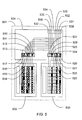
- FIG. 5 shows a preferred embodiment of the present invention for a memory circuit block.
- the memory circuit block 501 consists of two memory chips 502 , 503 , and a resistor group 504 .
- the resistor group contains four resistor networks, each with 4 resistors.
- the resistors 510 , 511 , 512 , 513 , 514 , 515 , 516 , and 517 link the data bit lines on the memory chip 502 to the memory bit lines 530 , 531 , 532 , 533 , 534 , 535 , 536 , and 537 on the memory circuit block.
- the resistors 520 , 521 , 522 , 523 , 524 , 525 , 526 , and 527 link the data bit lines on the memory chip 503 to the memory bit lines 530 , 531 , 532 , 533 , 534 , 535 , 536 , and 537 on the memory circuit block.
- memory bit positions D 1 , D 3 , D 4 , D 6 , and D 7 are marked as defective because they contain at least one defective memory blocks.
- the remaining bits D 0 , D 2 , and D 5 contains only functional memory blocks.
- Resistors 510 , 512 , and 515 with a low resistance value serve as connecting mechanisms to link the functional data bits D 0 , D 2 , and D 5 to the data lines 530 , 532 , and 535 of the circuit block.
- Resistors 511 , 513 , 514 , 516 , and 517 with a high resistance value serve as disconnecting mechanisms to block D 1 , D 3 , D 4 , D 6 , and D 7 from the circuit block data lines.
- memory bit positions D 0 , D 2 , D 5 are marked as defective because they contain at least one defective memory blocks.
- the remaining bits D 1 , D 3 , D 4 , D 6 , and D 7 contains only functional blocks.
- Resistors 521 , 523 , 524 , 526 , and 527 with a low resistance value serve as connecting mechanisms to link the functional data bits D 1 , D 3 , D 4 , D 6 , and D 7 to the data line 531 , 533 , 534 , 536 and 537 of the circuit block.
- Resistors 520 , 522 , and 525 with a high resistance value serve as disconnecting mechanisms to block D 0 , D 2 , D 5 from the circuit block data lines.
- FIG. 6 shows a preferred embodiment of the present invention for a memory module.
- the memory module 601 contains eight memory circuit blocks 602 .
- a memory circuit block 602 consists of two memory chips 603 , 604 , and a resistor group 605 .
- the resistors serve either as connecting mechanisms to link the functional chip data bit lines to the circuit block data bit lines or as disconnecting mechanisms to block the defective chip data bit lines from the circuit block data bit lines.
- the data bit lines on the memory circuit blocks are connected to the edge connector 606 of the memory module.
Landscapes
- Engineering & Computer Science (AREA)
- Microelectronics & Electronic Packaging (AREA)
- Dram (AREA)
Abstract
A method and apparatus provides resistor networks with two or more resistance values, which may accommodate different circuit configurations with a common circuit assembly. Also, the present invention provides a packaging method using multiple-value resistor networks as connecting and disconnecting mechanisms for the signal lines on the package.
Description
- This invention relates to resistor elements and resistor networks.
- Electronic circuit modules sometimes contain resistor networks to incorporate multiple resistors of the same value.
- A 64-bit memory module normally contains 16 resistor networks, each with 4 resistor elements with a value of 10 ohms.
- In order to construct usable memory module packages with partially defective memory chips, the on-board resistors are required to have certain combinations of values.
- Using 64 or 128 single individual resistors is certainly one way to accommodate this situation. However, the assembly process is more time consuming. It is also subject to certain limitation on the total number of onboard components.
- Using different printed circuit boards for different configurations is another way to cope with the situation. However, the inventory and production control becomes quite complex.
- This invention proposes a method and apparatus to generate resistor networks with multiple values.
- This invention provides a method to accommodate different component configurations with a single printed-circuit board.
- This invention further provides a method to simplify the manufacturing process of an electronic circuit module.
- FIG. 1 is a diagram of a prior art resistor network.
- FIG. 2 is a diagram of a prior art memory circuit block.
- FIG. 3 is a diagram of a prior art memory module.
- FIG. 4 shows a number of preferred embodiments of the present invention for a multiple-value resistor network.
- FIG. 5 shows a preferred embodiment of the present invention for a memory circuit block.
- FIG. 6 shows a preferred embodiment of the present invention for a memory module.
- The present invention will be illustrated with some preferred embodiments.
- FIG. 1 is a diagram of a prior art resistor network. The
resistor network 101 containsresistors - FIG. 2 is a diagram of a prior art memory circuit block. The
memory circuit block 201 consists of amemory chip 202 and aresistor group 203. The resistor group contains tworesistor networks - Each resistor network contains 4 resistor elements of the same value, 10 ohms. A resistor element serves as a connecting mechanism to link a
data bit line 206 on the memory chip to adata bit line 207 on the memory circuit block. - FIG. 3 is a diagram of a prior art memory module. The
memory module 301 contains eightmemory circuit blocks 302. Amemory circuit block 302 consists of amemory chip 303 and aresistor group 304. - The resistors serve as connecting mechanisms to link the data bit lines on the memory chips to the data bit lines on the memory circuit blocks. The data bit lines on the memory circuit blocks are connected to the
edge connector 305 of the memory module. - FIG. 4 shows a number of preferred embodiments of the present invention for a multiple-value resistor network.
- The
resistor network 401 containsresistors resistors resistor 414 has a different value, for example, 1 mega ohms. - FIG. 4 shows eight different combinations of multiple-value resistor networks with two different values. Shaded resistors are with a resistance value of 1 mega ohms. Blank resistors are with a resistance value of 10 ohms.
- There are a total of 16 ways to combine four resistors with two possible values. Besides the eight
combinations resistor networks - FIG. 5 shows a preferred embodiment of the present invention for a memory circuit block. The
memory circuit block 501 consists of twomemory chips resistor group 504. The resistor group contains four resistor networks, each with 4 resistors. - The
resistors memory chip 502 to thememory bit lines - The
resistors memory chip 503 to thememory bit lines - In
memory chip 502, memory bit positions D1, D3, D4, D6, and D7 are marked as defective because they contain at least one defective memory blocks. The remaining bits D0, D2, and D5 contains only functional memory blocks. -
Resistors data lines Resistors - In
memory chip 503, memory bit positions D0, D2, D5 are marked as defective because they contain at least one defective memory blocks. The remaining bits D1, D3, D4, D6, and D7 contains only functional blocks. -
Resistors data line Resistors - FIG. 6 shows a preferred embodiment of the present invention for a memory module. The
memory module 601 contains eightmemory circuit blocks 602. Amemory circuit block 602 consists of twomemory chips resistor group 605. - The resistors serve either as connecting mechanisms to link the functional chip data bit lines to the circuit block data bit lines or as disconnecting mechanisms to block the defective chip data bit lines from the circuit block data bit lines.
- The data bit lines on the memory circuit blocks are connected to the
edge connector 606 of the memory module.
Claims (9)
1. A resistor network package comprising:
(a) a plurality of external contact points;
(b) a plurality of first sub-packages each with a first resistance value between two external contact points;
(c) a plurality of second sub-packages each with a second resistance value between two external contact points;
wherein said first resistance value is different from said second resistance value;
wherein the difference between said first resistance value and said second resistance value is larger than 50% of the first resistance value.
2. The resistor network package of claim 1 wherein said first sub-package is a low-impedance material, a low-value resistor, a zero-ohm resistor, or a close-circuit connection.
3. The resistor network package of claim 1 wherein said second sub-package is a high-impedance material, a high-value resistor or an open-circuit condition.
4. An electronic circuit assembly comprising:
(a) a plurality of resistor network packages, at least one of which contains a first sub-package with a first resistance value between two external contact points and a second sub-package with a second resistance value between two external contact points, said second resistance value is different from the first resistance value by at least 50% of the first resistance value.
(b) a plurality of assembly signal lines;
(c) a circuit sub-assembly having a plurality of sub-assembly signal lines;
wherein at least one said sub-package in a resistor network package links one said sub-assembly signal line to one said assembly signal line.
5. The electronic circuit assembly of claim 4 wherein said first sub-package is a low-impedance material, a low-value resistor, a zero-ohm resistor, or a close-circuit connection.
6. The electronic circuit assembly of claim 4 wherein said second sub-package is a high-impedance material, a high-value resistor or an open-circuit condition.
7. An electronic circuit assembly comprising:
(a) a plurality of resistor network packages, at least one of which contains a first sub-package with a first resistance value between two external contact points and a second sub-package with a second resistance value between two external contact points, said second resistance value is different from the first resistance value by at least 50% of the first resistance value.
(b) a plurality of assembly signal lines;
(c) a first circuit sub-assembly having a plurality of first sub-assembly signal lines;
(d) a second circuit sub-assembly having a plurality of second sub-assembly signal lines;
wherein at least a first sub-package in a resistor network package links one said first sub-assembly signal line to a first said assembly signal line.
wherein at least a second sub-package in a resistor network package links one said second sub-assembly signal line to a second said assembly signal line.
8. The electronic circuit assembly of claim 7 wherein said first sub-package is a low-impedance material, a low-value resistor, a zero-ohm resistor, or a close-circuit connection.
9. The electronic circuit assembly of claim 7 wherein said second sub-package is a high-impedance material, a high-value resistor or an open-circuit condition.
Priority Applications (2)
| Application Number | Priority Date | Filing Date | Title |
|---|---|---|---|
| US10/119,005 US20030193387A1 (en) | 2002-04-10 | 2002-04-10 | Multiple-value resistor network |
| TW092200621U TW595798U (en) | 2002-04-10 | 2003-01-14 | Multiple-value resistor network for circuit connection control |
Applications Claiming Priority (1)
| Application Number | Priority Date | Filing Date | Title |
|---|---|---|---|
| US10/119,005 US20030193387A1 (en) | 2002-04-10 | 2002-04-10 | Multiple-value resistor network |
Publications (1)
| Publication Number | Publication Date |
|---|---|
| US20030193387A1 true US20030193387A1 (en) | 2003-10-16 |
Family
ID=28789899
Family Applications (1)
| Application Number | Title | Priority Date | Filing Date |
|---|---|---|---|
| US10/119,005 Abandoned US20030193387A1 (en) | 2002-04-10 | 2002-04-10 | Multiple-value resistor network |
Country Status (2)
| Country | Link |
|---|---|
| US (1) | US20030193387A1 (en) |
| TW (1) | TW595798U (en) |
-
2002
- 2002-04-10 US US10/119,005 patent/US20030193387A1/en not_active Abandoned
-
2003
- 2003-01-14 TW TW092200621U patent/TW595798U/en not_active IP Right Cessation
Also Published As
| Publication number | Publication date |
|---|---|
| TW595798U (en) | 2004-06-21 |
Similar Documents
| Publication | Publication Date | Title |
|---|---|---|
| EP1422717B1 (en) | Memory system and memory subsystem | |
| US8013448B2 (en) | Multiple selectable function integrated circuit module | |
| US6791157B1 (en) | Integrated circuit package incorporating programmable elements | |
| US5768173A (en) | Memory modules, circuit substrates and methods of fabrication therefor using partially defective memory devices | |
| US20010009032A1 (en) | Structure having multiple levels of programmable integrated circuits for interconnecting electronic components | |
| US5414638A (en) | Programmable interconnect architecture | |
| JPH0743674B2 (en) | Memory unit using partially good memory module and method of forming the same | |
| WO2005026957A3 (en) | Defect-tolerant and fault-tolerant circuit interconnections | |
| US4942453A (en) | IC package | |
| US5539976A (en) | System for manufacture of hybrid integrated circuit | |
| US6449170B1 (en) | Integrated circuit package incorporating camouflaged programmable elements | |
| US6732266B1 (en) | Method and apparatus for reconfiguring circuit board and integrated circuit packet arrangement with one-time programmable elements | |
| US6890184B2 (en) | Electrical connector for conveying signals between two circuit boards | |
| US20030193387A1 (en) | Multiple-value resistor network | |
| US20030214383A1 (en) | Resistor network package | |
| US4674007A (en) | Method and apparatus for facilitating production of electronic circuit boards | |
| US6222211B1 (en) | Memory package method and apparatus | |
| US7055069B2 (en) | Spare input/output buffer | |
| US7260671B2 (en) | Information containing means for memory modules and memory chips | |
| US6947303B2 (en) | Memory chip, memory component and corresponding memory module and method | |
| US6839241B2 (en) | Circuit module | |
| US20050052854A1 (en) | Configurable circuit board and fabrication method | |
| US20010031507A1 (en) | Method and device for adapting/tuning signal transit times on line systems or networks between integrated circuits | |
| US20030157816A1 (en) | Apparatus for connecting semiconductor modules | |
| GB2291992A (en) | Method of producing memory modules using partial memory circuits |
Legal Events
| Date | Code | Title | Description |
|---|---|---|---|
| STCB | Information on status: application discontinuation |
Free format text: ABANDONED -- FAILURE TO RESPOND TO AN OFFICE ACTION |