US20030192020A1 - Slack time analysis through latches on a circuit design - Google Patents
Slack time analysis through latches on a circuit design Download PDFInfo
- Publication number
- US20030192020A1 US20030192020A1 US10/319,018 US31901802A US2003192020A1 US 20030192020 A1 US20030192020 A1 US 20030192020A1 US 31901802 A US31901802 A US 31901802A US 2003192020 A1 US2003192020 A1 US 2003192020A1
- Authority
- US
- United States
- Prior art keywords
- latch
- time
- arrival
- path
- node
- Prior art date
- Legal status (The legal status is an assumption and is not a legal conclusion. Google has not performed a legal analysis and makes no representation as to the accuracy of the status listed.)
- Granted
Links
Images


Classifications
-
- G—PHYSICS
- G06—COMPUTING OR CALCULATING; COUNTING
- G06F—ELECTRIC DIGITAL DATA PROCESSING
- G06F30/00—Computer-aided design [CAD]
- G06F30/30—Circuit design
- G06F30/32—Circuit design at the digital level
- G06F30/33—Design verification, e.g. functional simulation or model checking
- G06F30/3308—Design verification, e.g. functional simulation or model checking using simulation
- G06F30/3312—Timing analysis
Definitions
- the invention relates to methods of deriving timing information for circuits, and more particularly to deriving slack times in circuits comprising latches.
- a flip-flop receives a data signal on an input data terminal.
- the input data terminal is typically denoted by the symbol D.
- the flip-flop Upon receiving a clock signal on a clock terminal, the flip-flop stores (latches) the data signal and provides the data signal on an output data terminal.
- the clock terminal is typically denoted by the symbol CK
- the output data terminal is typically denoted by the symbol Q.
- the data signal is latched upon the occurrence of an edge of the clock signal.
- terminal and “pin” may be considered interchangeable.
- a latch operates in a manner similar to a flip-flop, except that the latch is “open” during substantially the entire interval while the clock signal is asserted.
- the signal propagates from D through the latch to Q during substantially the entire time while the clock signal is asserted.
- the latch “closes”, e.g. the signal from D is no longer propagated to Q.
- the Q terminal retains the value of the signal at D when the latch closed.
- the setup time is the period of time during which the data signal must be stable before the clock signal arrives at CK. This is referred to as the setup time.
- the data signal must arrive at D and be stable there for a period of time equal to or exceeding the setup time in order for the data signal to be properly latched. Both flip-flops and latches are characterized by setup times.
- the triggering edge of the clock signal is the clock signal edge that causes the flip-flop to latch the data signal.
- the triggering edge may be either the rising or falling edge of the clock signal.
- the edge of the clock signal that causes the latch to open is referred to as the opening edge of the latch.
- the edge of the clock signal that causes the latch to close is referred to as the closing edge of the latch.
- the rising edge of the clock signal may serve as either the opening or closing edge of a latch.
- the falling edge of the clock signal may serve as either the opening or closing edge of a latch.
- Flip-flops and latches are clocked devices typically employed as sequential circuit elements. The timing of their operation is controlled by the timing of the clock signal. Non-clocked devices are also typically found in circuits. Such devices operate independently of a clock signal, and may be referred to collectively as “combinational” circuit elements. Examples of combinational elements include logic gates (AND, OR, inverter, NOR, NAND, etc. gates). Both clocked and combinational circuit elements have an associated propagation delay.
- the propagation delay of flip-flops and latches is the time that it takes the data signal to propagate from D to Q, once the clock signal is received at CK.
- the propagation delay of combinational elements, and collections thereof is the time it takes for changes in the data signal(s) to the combinational elements to be reflected at the output(s) of the combinational elements.
- a circuit element may be characterized by different propagation delays for high-low (falling) and low-high (rising) signal transitions.
- an AND gate in a circuit may be characterized by a first input-to-output propagation delay for rising input signals, and second input-to-output propagation delay for falling input signals.
- the propagation delay of a flip-flop is typically specified in terms of the time it takes a data signal at the D terminal to reach the Q terminal after the clock signal arrives at the CK terminal. This propagation delay may be referred to as the CK-Q delay of the flip-flop.
- One propagation delay of a latch is typically specified in terms of the time it takes a data signal at the D terminal to reach the Q terminal after the opening clock edge arrives at the CK terminal. This propagation delay may be referred to as the CK-Q delay of the latch.
- the CK-Q delay of the latch may be employed in situations where the data signal arrives at the D terminal of a closed latch.
- Another propagation delay of a latch is typically specified in terms of the time it takes a data signal at the D terminal to reach the Q terminal when the data signal arrives at the D terminal of an open latch. This propagation delay may be referred to as the D-Q delay of the latch.
- An important consideration for circuit designers is the tolerance for signal delays inherent in a circuit design. For example, in a circuit including a latch, it may be important for the circuit designer to know that the data signal arrives at D of the latch within the setup time of the latch, with five nanoseconds to spare. This spare time may be referred to as the “slack time” of the latch in the circuit in question. Among other things, the slack time for an element tells the designer whether the circuit design can tolerate additional delays in the data signal prior to the element.
- upstream in relation to a circuit element, refers to points in a circuit that a signal of interest reaches before it reaches the element.
- Downstream refers to points in the circuit that the signal reaches after it reaches the element.
- a slack time may be positive, indicating that there is some spare time built into the timing.
- a slack time may also be negative, indicating that signals do not propagate in sufficient time to meet the timing requirements of the circuit.
- Slack times at an input of a latch in a circuit design are determined by determining a set of required times at the input of the latch, where the set of required times includes a required time entry for each different relationship between a signal comprising a downstream reference event and a clock signal for the latch.
- a set of arrival time entries at the input of the latch is also determined, each arrival time entry having a corresponding required time entry.
- the required times are propagated upstream from a final event of interest to a source event of interest.
- the arrival times are propagated downstream from the source event of interest to the final event of interest.
- Slack path analysis on the circuit design is performed by organizing starting points of paths through the circuit design into a queue. Slack times are determined at the points, and the queue is ordered according to the slack times. A path having a lowest slack time is removed from the top of the queue. When the path is not complete, it is extended and a slack time is determined at a new end point of the path. The path is replaced at a location in the queue such that the queue remains ordered.
- FIG. 1 is a block diagram of an embodiment of a circuit design.
- FIG. 2 is a graph of signal propagation through the circuit design of FIG. 1.
- FIG. 3 illustrates embodiments of clock signals to the circuit design of FIG. 1.
- FIG. 4 illustrates embodiment of periodic signals having edges in multiple relationships.
- FIG. 5 illustrates a method embodiment to locate corresponding edges of periodic signals.
- FIG. 6 is a flow chart of a method embodiment to locate corresponding edges of periodic signals.
- FIG. 7 is a block diagram illustrating a method embodiment to determine required times at points in a circuit design.
- FIG. 8 illustrates embodiments of signals for the circuit design of FIG. 7.
- FIG. 9 is a block diagram illustrating a method embodiment to determine arrival times at points in the circuit design of FIG. 7.
- FIG. 10 illustrates a circuit element wherein signals are merged.
- FIG. 11 illustrates embodiments of an ideal signal and slewed signals.
- FIG. 12 is a flow chart of an embodiment of a method to perform slack analysis on a circuit design.
- FIG. 13 illustrates a circuit element wherein fan out takes place.
- FIG. 14 is a block diagram of an embodiment of a network environment for performing slack time analysis of a circuit design.
- FIG. 15 is a block diagram of an embodiment of a system to carry out methods in accordance with the present invention.
- a first flip-flop 102 receives a signal S on input terminal D 1 .
- the flip-flop 102 receives a first clock signal edge C 1 on clock terminal CK 1 .
- the output terminal Q 1 of the flip-flop 102 is coupled to the input terminal D 2 of the latch 107 by way of combinational logic 104 .
- the combinational logic 104 is represented by a single symbol but may comprise numerous gates in various configurations.
- the latch 107 receives a second clock signal edge C 2 on the clock terminal CK 2 .
- the output terminal Q 2 of the latch 107 is coupled to the input terminal D 3 of a second flip-flop 108 by way of combinational logic 106 .
- the combinational logic 106 is represented by a single symbol but may comprise numerous gates in various configurations.
- the flip-flop 108 receives a third clock signal edge C 3 on clock terminal CK 3 .
- the first flip-flop 102 is upstream from the second flip-flop 108 .
- the first flip-flop 102 may be referred to as the “source” flip-flop, and the second flip-flop 108 may be referred to as the “destination” flip-flop.
- the signal S propagates over time through various points in the circuit. First, the signal S arrives at node A. Upon the occurrence of C 1 at node B, S propagates through the flip-flop 102 to node C.
- Flip-flop 102 has a CK-Q propagation delay of P 1 , so that S arrives at C a time P 1 after the occurrence of C 1 at B.
- Signal S then propagates from C to D, arriving at D after the propagation delay P 2 of logic 104 .
- the signal S propagates to F after incurring the propagation delay P 3 of the latch 107 .
- the delay P 3 to apply is either the CK-Q delay of the latch 107 (if the signal S arrives at D before the occurrence of clock signal C 2 at E, e.g. when the latch 107 is closed), or else the delay is the D-Q delay if the signal S arrives at D after the clock signal C 2 , e.g. after the latch 107 opens.
- Signal S then propagates from F to G, arriving at G after the propagation delay P 4 of the logic 106 .
- the propagation delays P 1 , P 2 , P 3 , and P 4 may all vary according to whether or not the propagating event is a rising or falling edge of the signal S.
- FIG. 2 illustrates only one of many possible timing scenarios for the circuit 100 .
- S propagates from points A to C to D.
- the signal S is blocked at D (the input of the latch 107 ) until such time as the edge C 2 occurs, at which point S propagates to point F and on to point G.
- Other timing scenarios are also possible.
- the signal S may not be blocked at point D (the input of the latch 107 ), but may instead pass through the latch 107 without being blocked for any period of time.
- a signal is blocked at the input of a latch, it is a “red light” condition.
- a signal reaches the input of a latch and propagates through without being blocked for any period of time, it is a “green light” condition.
- FIG. 3 illustrates a possible timing relationship between the edges of three clock signals; Clock 1 , Clock 2 , and Clock 3 .
- the signal Clock 1 has a period of 20 and is high from the time 0 to the time 10. Signal Clock 1 is then low from time 10 to time 20.
- the signal Clock 2 also has a period of 20, but is high from a time 5 to a time 15, and low from 15 to 25.
- the signal Clock 3 has a period of 20 and is high from times 14 to 19, and low from times 19 to 34. Given this timing relationship among the clock signals, it is possible to compute slack times for points in the circuit 100 by assigning values to the various propagation delays of the elements.
- the slack time at point G is the difference between when S actually arrives at point G, and the latest time S could have arrived at point G and still met the timing of the circuit. Thus the slack time at point G is:
- a “path” is a set of related events at different points in a circuit.
- the points in a path are related by a common signal that passes through them without stopping. If a signal gets to a latch when it is closed, that path stops there. A new path starts at the enable pin when the latch opens.
- the slack time of a path is the slack time at the end of the path (the slack time as determined for the path at the final point in the path).
- Paths provide useful information about circuit timing behavior, including slack times at points in the circuit. To determine the slack times at points along a path, an event of interest is selected at the end point of the path. This event is referred to herein as the “final event of interest”.
- the final event of interest is the occurrence of the edge C 3 at the flip-flop 108 .
- an event of interest is determined corresponding to the final event of interest. This corresponding event of interest is referred to herein as the “starting event of interest”.
- the starting event of interest is the occurrence of edge C 1 .
- the slack time will be the same at all the points.
- the interval of time between the starting event of interest and the final event of interest bears upon the slack times at points along the path connecting the events.
- two periodic signals comprising the events of interest are “walked” in time to identify all possible relationships between the edges of the signals. For example, if the starting event of interest is a rising edge of a first clock signal, the first clock signal is traversed in time and each rising edge is examined against the corresponding (following most closely in time) rising edge of the second clock signal comprising the final event of interest.
- Each different timing relationship between the edges is recorded for purposes of determining slack times along the path between the events, when latches are involved. In a path without latches, only the timing relationship with the shortest time in between events is recorded, because that represents the worst slack time.
- the timing of the open intervals of the intervening latches becomes a consideration when determining the worst-case slack time of the path.
- the situation in which the latch clock signal and the destination flip-flop clock signal are closest in time may not lead to the worst-case slack situation for the path. Rather, a “back propagation” of required times for each possible relationship among the clocks may be performed, from the final event of interest to the source event of interest. In other words, starting with the required time of the final event of interest, required times are determined at successive neighboring points upstream in the path to keep track of possible relationships among the clocks encountered thus far.
- the final event of interest is a rising (trigger) edge of Clock 3
- the signal Clock 3 is periodic.
- the rising edge selected as the final event of interest has a required time.
- the latch 107 is encountered between points D and F in the path. Recall that the latch 107 propagates the signal S from point D to point F during the interval when the latch clock signal, e.g. Clock 2 , is high.
- the required time for the signal S to reach point D occurs some time before the falling (closing) edge of Clock 2 corresponding to the rising (trigger) edge of Clock 3 that was selected as the final event of interest.
- a process known as “ping-pong” may be employed to identify an edge to reference this required time to.
- FIG. 5 illustrates the ping-pong process. At 502 the closest rising (opening) edge of Clock 2 preceding the selected edge of Clock 3 is selected (the ‘ping’). At 504 the falling (closing) edge of Clock 2 following this opening edge is determined (the ‘pong’).
- This process is illustrated in flow chart form in FIG. 6.
- the closest opening edge of the upstream signal preceding the edge of the downstream signal is selected.
- the closing edge of the upstream signal following this opening edge is determined.
- the earlier in time of the closing edge of the upstream signal and the edge of the downstream signal is chosen as the event of interest upon which the required time at a point is referenced.
- the two signals are walked using the process described previously in conjunction with FIG. 4.
- a required time is determined for the signal S at point D for each possible different relationship between a rising edge of Clock 3 and a corresponding rising edge of Clock 2 . All of these required times are then propagated back along the path, along with a corresponding event to which they are referenced, until the source flip-flop 102 is reached, or until another latch is encountered in the path.
- the corresponding reference event is either the rising edge of Clock 3 or the corresponding falling edge of Clock 2 , whichever is earlier in time.
- a circuit embodiment 700 comprises a source flip-flop FF 1 having a clock Clock 1 , a destination flip-flop FF 2 having a clock Clock 4 , and two intervening latches L 1 and L 2 having clocks Clock 2 and Clock 3 , respectively.
- a final event of interest is selected. Let us choose, for example, the edge E 14 of Clock 4 .
- a signal S that arrives at point C must arrive before E 14 arrives at the clock terminal of the flip-flop FF 2 in order to be stored by the flip-flop FF 2 .
- the signal S must arrive at sufficient time before Clock 4 to meet the setup time of the flip-flop FF 2 .
- the setup times of the circuits will be overlooked, however, in practical applications the required times determined at each point in the circuit would reflect the setup times of the circuit elements.
- T RC1 The required time at C is recorded as T RC1 , e.g. the required time for signal S at point C in the circuit.
- the setup time of the flip-flop FF 2 is factored into T RC1 , so that for example if the flip-flop FF 2 has a 1 nanosecond setup time, T RC1 is ⁇ 1, e.g. 1 nanosecond sooner than the arrival of C 4 .
- T RC1 is ⁇ 1, e.g. 1 nanosecond sooner than the arrival of C 4 .
- latch L 2 is encountered.
- Latch L 2 is clocked by signal Clock 3 .
- FIG. 8 shows signal embodiments illustrating possible relationships between Clock 1 , Clock 2 , Clock 3 , Clock 4 .
- Clock 1 has a period of 30 and rising edges at 10 , 40 , 70 , and 100 .
- Clock 1 has falling edges at 15 , 45 , 75 , and 105 .
- Clock 2 has a period of 120 , with four pulses per period, and rising edges at 15 , 46 , 76 , and 104 .
- Clock 2 has falling edges at 22 , 51 , 83 , and 113 .
- Clock 3 has a period of 60 , with two pulses per period, and rising edges at 20 , 52 , 80 , and 112 .
- Clock 3 has falling edges at 24 , 57 , 84 , and 117 .
- Clock 4 has a period of 30 and rising edges at 25 , 55 , 85 , and 115 .
- Clock 4 has falling edges at 28 , 58 , 88 , and 118 .
- edge E 9 of Clock 3 corresponds to (is the closest preceding edge in time) edge E 13 of Clock 4 .
- edge E 13 is used to clock the flip-flop FF 2 , then edge E 9 is presumed to be the edge that will open the preceding latch L 2 .
- Edge E 10 of Clock 3 corresponds to edge E 14 of Clock 4 .
- the other edges of Clock 3 and Clock 4 have the same relationship (e.g. the same relative timing) as edges E 9 /E 13 and E 10 /E 14 .
- the signals Clock 3 and Clock 4 have two possible relationships.
- the “virtual period” of the two clock signals Clock 4 and Clock 3 is determined as the least common multiple of the clock periods of the two signals. In this case, the virtual period is 60.
- two required times are recorded for point B in the circuit 700 , one required time for each possible relationship between the signals Clock 3 and Clock 4 .
- the required times at point B are determined using the D-Q propagation delay of the intervening latch.
- a first required time entry T RB1 is recorded for point B.
- a reference event in this case E 9 ′, is associated with this required time relative to E 13 (because required times are only significant in relation to some event).
- the interval ⁇ E 9 , E 9 ′> is also associated with the required time and like the required time is made relative to the reference event (e.g. the start and stop times of the interval are each made relative to the time of the reference event E 9 ′).
- the purpose of recording the latch open interval with the required time will be explained subsequently.
- a second required time entry T RB2 is recorded for point B.
- a reference event in this case E 14
- E 14 is associated with this required time relative to E 14 .
- the interval ⁇ E 10 , E 14 > is also associated with the required time and like the required time is made relative to the reference event.
- the interval is ⁇ E 10 , E 14 >, not ⁇ E 10 , E 10 ′>, because E 14 occurs at 55 ns and E 10 ′ occurs at 57 ns.
- the set of reference edges at a point in a path may be referred to as a “virtual clock edge list” at the point in the path.
- the reference event for required times at a point preceding a latch is a closing edge of the latch clock signal when the latch closes prior to the occurrence of the corresponding downstream event.
- required times are determined for point A, based upon the required times determined for point B.
- the latch L 1 is clocked by signal Clock 2 .
- the edges of Clock 2 have four possible relationships with the set of reference signals determined at point B.
- the required times associated with the reference edges E 5 ′, E 6 ′, E 7 ′, and E 8 ′ are the ones that would have been originally from edges E 13 , E 14 , E 15 , and E 16 respectively.
- the virtual period of the signals comprising the reference edges at point B is 60.
- the required time T RB1 at point B is referenced to the edge E 9 ′ of signal Clock 3 .
- a required time T RA1 at point A is determined by adjusting the required time T RB1 to be relative to the reference edge at point A.
- Edge E 5 ′ is chosen as the reference edge at point A using the ping-pong approach.
- An interval ⁇ E 9 ,E 5 ′> is associated with T RA1 , representing the composite (overlap) of the latch open intervals ⁇ E 9 ,E 9 ′>and ⁇ E 5 ,E 5 ′>.
- a required time T RA2 is recorded at point A, corresponding to the required time T RB1 plus one virtual period of the signals comprising the reference edges at point B.
- One virtual period (60) was added to the reference edge E 9 ′ to determine the corresponding reference edge E 11 ′ from the next virtual period of Clock 3 .
- the reference event is set to E 7 ′.
- a composite open interval ⁇ E 11 ,E 7 ′> is associated with T RA2 , representing the overlap of the latch open intervals ⁇ E 11 ,E 11 ′>and ⁇ E 7 ,E 7 ′>. Adjustments for circuit delay are made in the manner described above. The intervals are made relative to the same reference edge, as described above.
- the required time T RA3 at point A represents a third relationship between the edges of Clock 2 and Clock 3 .
- the reference event for T RA3 is set to E 6 ′.
- There is no interval of time during which the open intervals ⁇ E 10 ,E 10 ′>and ⁇ E 6 ,E 6 ′>overlap (assume for the purpose of this description that this is true, even after adjusting for circuit delay and making the intervals relative to E 6 ′).
- the composite open interval is set to undefined (!).
- a fourth required time T RA4 is recorded at point A, corresponding to the required time T RB3 plus one virtual period of the signals comprising the reference events at point B.
- the reference event for T RA4 is determined to be E 8 ′.
- a composite open interval ⁇ E 12 ,E 8 ′> is associated with T RA4 , representing the overlap of the latch open intervals ⁇ E 12 ,E 12 ′>and ⁇ E 8 ,E 8 ′>. Again, circuit delays are ignored, and the intervals are made relative to E 8 ′ in determining the overlap.
- the signal Clock 1 is the clock signal for flip-flop FF 1 .
- a corresponding arrival time is determined at point X, where Clock 1 is received.
- a particular required time entry at point A may give rise to multiple arrival time entries at point X.
- Edges of Clock 1 are chosen that immediately precede each of the required times. In this manner, each back propagated required time and event of interest is associated with a source event of interest at the starting point of the path.
- Each required time is associated with one or more starting events of interest. If the number of starting events of interest is greater than one, then the relationship of one or more virtual periods is different with respect to the source clock.
- the source events of interest identified in this fashion may then be propagated downstream along the path. Any uncertainty in the arrival time of a source event at point X is accounted for as an interval (T1, T2) of potential arrival times for the source event, where T1 is the earliest possible arrival time for the event, and T2 is the latest possible arrival time for the event.
- Arrival times for the source events of interest at various points downstream are determined by adding propagation delays of the elements encountered by the events as they propagate downstream. Each element can have a minimum and maximum propagation delay.
- the arrival ranges are “widened” according to the maximum propagation delay of the elements encountered. To widen a range, T1 is increased by the minimum propagation delay of the element, and T2 is increased by the maximum propagation delay of the element.
- entries may be merged to determine the arrival time entries at the next downstream point after the latch.
- the arrival time entry (T1 AA1 , T2 AA1 , E 5 ′) corresponds to the required time entry (T RA1 , E 5 ′, ⁇ E 9 ,E 5 ′>);
- the arrival time entry (T1 AA2 , T2 AA2 , E 7 ′) corresponds to the required time entry (T RA2 , C 4 ′, ⁇ E 11 ,E 7 ′>); and so on.
- arrival time entries corresponding to required time entries with a common parent are merged to create an arrival time entry at the next downstream point after the latch.
- the two arrival time entries (T1 AA1 , T2 AA1 , E 5 ′) and (T1 AA2 , T2 AA2 , E 7 ′) at point A are merged to create the arrival time entry at point B, (T1 AB1 , T2 AB1 , E 9 ′).
- the value T1 AB1 is determined as the minimum of T1 AA1 and T1 AA2 .
- the value T2 AB1 is determined as the maximum of T2 AA1 and T2 AA2 .
- the arrival time intervals are made relative to (referenced to) the reference event of the corresponding parent event.
- the values T1 AB1 and T2 AB1 are adjusted so that they are relative to edge E 9 ′ before performing the merge.
- Making the times relative to E 9 ′ involves an adjustment (in the case of arrival times T1 AA1 and T2 AA1 relative to E 5 ′, adding or subtracting the difference between E 5 ′ and E 9 ′) and a translation (in the case of the arrival times T1 AA2 and T2 AA2 relative to E 7 ′, making them relative to E 11 ′).
- the arrival range relative to E 9 ′ represents the range of all possible arrivals that could arrive relative to E 9 ′ or any clock edge related to E 9 ′ by the virtual clock period at point B.
- the interval (T1 AB1 , T2 AB1 ) is widened according to the minimum and maximum propagation delays of the latch L 1 .
- the interval (T1 AB1 , T2 AB1 ) is “clipped” according to the relevant open interval of the latch L 1 . Clipping involves finding the overlap of the two intervals.
- the reference event is edge E 9 ′
- the corresponding open interval of latch L 1 is ⁇ E 5 ,E 5 ′>.
- the reference event is edge E 14
- the corresponding open interval of latch L 1 is ⁇ E 6 ,E 6 ′>.
- the two arrival time entries (T1 AA3 , T2 AA3 , E 6 ′) and (T1 AA4 , T2 AA4 , E 8 ′) at point A are merged and adjusted to create the arrival time entry at point B, (T1 AB2 , T2 AB2 , E 14 ).
- a situation may arise where the arrival interval and the open interval of the latch do not overlap. If the arrival interval ends before the open interval begins, the signal S always hits a red light at the latch. In this case, the path from point X is ended at point A, and a new path is started from point Y. The source events of interest for this new path are the edges of the clock signal Clock 2 .
- the signal S may hit a red light at the latch.
- the path from point X is ended at point A, and an identical path from point X is continued on through the latch (using the CK-Q propagation delay of the latch).
- Another path is started from point Y.
- the source events of interest for this new path are the edges of the clock signal Clock 2 .
- Slack times for the path ending at A are determined relative to the closing edge of the latch clock, providing a slack value that is relevant for the path up to that latch but not beyond.
- arrival entries will be recorded at X only for those edges of Clock 2 resulting in red-light conditions at point A. For example, if there are 6 different clock relationships between the latch clock and the clocks comprising the reference events at a latch, if only on the fifth relationship involves a red-light situation, then an arrival entry and a path from the latch clock terminal to the latch output terminal will be produced only for that fifth relationship. In other words, for each reference event at the data terminal of a latch, a decision is made as to whether or not to begin a new path at the clock terminal of the latch. If an arrival entry gives rise to a red light situation, paths are started from the clock terminal of the latch and proceeding downstream through the design for each arrival at the latch clock terminal that gives rise to a red light situation. Other arrivals at the clock terminal do not give rise to new paths.
- a “period offset” may be included with the arrival entries.
- the period offset associated with an arrival entry indicates which period of the virtual clock for the reference event comprised by the arrival entry had the earliest arrival time.
- the period offset indicates from which virtual period of the reference event the red-light situation arose.
- the period offset is increased appropriately when merging arrival entries.
- the period offsets there are set based on the period offsets of the arrival entries at the latch data terminal that gave rise to the red light condition. The period offset is used when a path is started at the clock pin of a latch to begin the path an appropriate number of iterations of the virtual period out to correspond with the red light arrival.
- each arrival entry may also comprise a minimum late value and a maximum early value. These values may be applied to ascertain when to start a path at the latch clock terminal or the latch output terminal in situations where multiple signals merge coming to the input terminal of the latch.
- the two arrival time entries at point B are merged to create the arrival time entry at point C, (T1 AC1 , T2 AC1 ).
- the interval (T1 AC1 , T2 AC1 ) is widened according to the minimum and maximum propagation delays of the latch L 2 .
- the interval (T1 AC1 , T2 AC1 ) is “clipped” according to the relative open interval of the latch L 2 . Paths are terminated at point B, and new paths created, according to the same process specified for point A.
- a circuit element 1050 has two inputs having points A and B, respectively. Signals S 1 and S 2 arrive at points A and B, respectively. Arrival intervals (T1 A , T2 A ) and (T1 B , T2 B ) are determined for signals S 1 and S 2 at points A and B, respectively. One of these intervals is referenced to the reference event of the other, each interval is adjusted for the corresponding propagation delay through the element 1050 (A to C delay and B to C delay), and then the two intervals are merged to produce the arrival interval (T1 c , T2 c ) at point C.
- signals S 1 and S 2 each have a best-case and worst-case slew time. Assuming that a signal transition is complete when the signal crosses the midpoint of its low-high range, then the rising edge of signal S 1 occurs, in the worst case, at time t1 and in the best case at time t2. The rising edge of signal S 2 occurs, in the best case, at time t3 and in the worst case at time t4. To merge the arrival intervals of these two signals, the delay range from A to C is calculated using the best and worst case slews for signal S 1 . The delay range from B to C is calculated using the best and worst case slews for signal S 2 .
- the two delay ranges are merged to determine the arrival ranges of the signal at C.
- the slew range of the merged signal is set to the worst-case slew of signal S 1 (which is worse than the worst case slew of signal S 2 ).
- FIG. 12 shows a method embodiment 1200 for reporting paths with worse-case slack time in a circuit.
- the starting points for all paths through a circuit are added to a priority path queue.
- a priority queue is an ordered collection.
- a particular point may be the starting point for multiple paths.
- a starting point may comprise multiple sets of required and arrival times determined according to the preceding analysis. Starting points are added for the rising and falling edges of the signal to trace through the design.
- slack times are determined at each starting point according to the required time and arrival time entries.
- an arrival time for each possible clock relationship is carried from the source clock all the way through the pipeline of latches.
- Each of these arrivals is updated appropriately as the path is extended.
- Each arrival can be compared with a required time at the current end point of the path by an appropriate adjustment.
- By examining each arrival as it passes through a latch it can be determined whether or not the late value will pass through the latch. If so, the path continues. If not, the path is left undefined. The worst-case of the slack times determined in this fashion is the slack time of the path.
- the queue is ordered at 1206 according to slack time.
- the queue could be “self-ordering”, so that as paths are added, the queue reorders itself so that it is always ordered according to the slack time of its constituent paths.
- the path with the lowest (worst-case) slack time is placed at the head of the queue.
- the slack time of paths increases from the head of the path queue to the tail of the path queue.
- the path at the head of the path queue (the path having the worst slack time) is removed from the path queue.
- a check is made to determine if this path is a complete path, e.g. if it has been extended to its ending point. If so, the path is “reported” by moving it to the report queue at 1210 .
- This report queue is provided to the circuit designer and is self-ordering; that is, the first path moved to the report queue has the worst slack, the next path moved to the report queue has the second worst slack, and so on. Processing may stop once a number of worst case slack paths, as specified by the circuit designer, are reported.
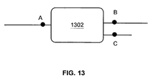
- FIG. 13 shows an example of a fan out situation.
- a circuit element 1302 has a single input and two outputs.
- a fan out occurs so that the output signal of the circuit 1302 is provided at both points B and C.
- the path is cloned (the path information is duplicated) to create one new, identical path.
- the existing path is extended from point A to point B, and the new path is extended from A and C.
- slack times are computed at the end points of the paths and the paths are inserted into the path queue at the proper location, e.g. placed such that the ordering of the queue is maintained.
- each arrival range is examined to determine if the latest arrival time for the range falls within the open interval of the latch. If it does, the path is extended though the latch. Otherwise, the path is left undefined.
- the method then returns to 1208 to repeat, as long as the path queue is not empty, until a predetermined number of completed paths are removed to the report queue. This provides the circuit designer with a predetermined number of worst-case slack paths through the circuit.
- information comprising a circuit design may be communicated from a client device 1402 to a server device 1404 via a network 1406 .
- the network 1406 may comprise various technologies, including switches, routers, and computers of the Internet, the public phone network, and private collections of computers (so-called “intranets”). Optical, electrical, and wireless communication technologies may be employed, among other things.
- the client 1402 may be any processing device capable of storing and communicating information, such as a desktop computer, workstation, laptop computer, handheld computer, and so on.
- the server 1404 is any device comprising a process and memory that provides processing and/or data in response to requests from the client 1402 . Often, the server 1404 is some form of powerful computer system.
- the server 1404 may perform processing on the circuit information provided by the client 1402 and may communicate a resulting slack analysis to the client 1402 .
- an apparatus embodiment 1500 for practicing embodiments of the present invention comprises a processing unit 1502 (e.g., a processor, microprocessor, micro-controller, etc.) and machine-readable media 1504 .
- the apparatus may is an embodiment of a “computer system”, although in general a computer system can be any device comprising a processor and a memory, the memory to store instructions to supply to the processor for execution.
- the memory 1504 may be volatile (such as RAM), non-volatile (such as ROM, flash memory, etc.) or some combination of the two.
- the machine readable media 1504 may comprise volatile and/or nonvolatile media, removable and/or non-removable media, including: RAM, ROM, EEPROM, flash memory or other memory technology, CD-ROM, digital versatile disks (DVD) or other optical storage, magnetic cassettes, magnetic tape, magnetic disk storage or other magnetic storage devices, or any other medium which can be used to store the desired information to be accessed by the apparatus 1500 .
- the machine readable media 1504 may be implemented in any method or technology for storage of information such as computer readable instructions, data structures, program modules or other data. Such instructions and data may, when executed by the processor 1502 , carry out embodiments of methods in accordance with the present invention.
- the apparatus 1500 may comprise additional storage (removable 1506 and/or non-removable 1507 ) such as magnetic or optical disks or tape.
- the apparatus 1500 may further comprise input devices 1510 such as a keyboard, pointing device, microphone, etc., and/or output devices 1512 such as display, speaker, and printer.
- the apparatus 1500 may also typically include network connections 1520 (such as a network adapter) for coupling to other devices, computers, networks, servers, etc. using either wired or wireless signaling media.
- the components of the device may be embodied in a distributed computing system.
- a terminal device may incorporate input and output devices to present only the user interface, whereas processing component of the system are resident elsewhere.
- processing functionality may be distributed across a plurality of processors.
- the apparatus may generate and receive machine readable instructions, data structures, program modules or other data in a modulated data signal such as a carrier wave or other transport mechanism.
- modulated data signal means a signal that has one or more of its characteristics set or changed in such a manner as to encode information in the signal. This can include both digital, analog, and optical signals.
- communication media includes wired media such as a wired network or direct-wired connection, and wireless media such as acoustic, RF, infrared and other wireless media. Communications media, including combinations of any of the above, should be understood as within the scope of machine readable media.
Landscapes
- Engineering & Computer Science (AREA)
- Computer Hardware Design (AREA)
- Physics & Mathematics (AREA)
- Theoretical Computer Science (AREA)
- Evolutionary Computation (AREA)
- Geometry (AREA)
- General Engineering & Computer Science (AREA)
- General Physics & Mathematics (AREA)
- Synchronisation In Digital Transmission Systems (AREA)
- Logic Circuits (AREA)
Abstract
Description
- The invention relates to methods of deriving timing information for circuits, and more particularly to deriving slack times in circuits comprising latches.
- Flip-flops and latches are common elements of circuits. A flip-flop receives a data signal on an input data terminal. The input data terminal is typically denoted by the symbol D. Upon receiving a clock signal on a clock terminal, the flip-flop stores (latches) the data signal and provides the data signal on an output data terminal. The clock terminal is typically denoted by the symbol CK, and the output data terminal is typically denoted by the symbol Q. The data signal is latched upon the occurrence of an edge of the clock signal. Herein, the terms “terminal” and “pin” may be considered interchangeable.
- A latch operates in a manner similar to a flip-flop, except that the latch is “open” during substantially the entire interval while the clock signal is asserted. In other words, for a latch, the signal propagates from D through the latch to Q during substantially the entire time while the clock signal is asserted. When the clock signal is no longer asserted, the latch “closes”, e.g. the signal from D is no longer propagated to Q. The Q terminal retains the value of the signal at D when the latch closed.
- After the clock signal arrives at CK, the data signal must remain stable for the hold time in order for the data signal to be properly latched. This is true for both flip-flops and latches. Another consideration is the period of time during which the data signal must be stable before the clock signal arrives at CK. This is referred to as the setup time. The data signal must arrive at D and be stable there for a period of time equal to or exceeding the setup time in order for the data signal to be properly latched. Both flip-flops and latches are characterized by setup times.
- For a flip-flop, the triggering edge of the clock signal is the clock signal edge that causes the flip-flop to latch the data signal. The triggering edge may be either the rising or falling edge of the clock signal. For a latch, the edge of the clock signal that causes the latch to open is referred to as the opening edge of the latch. The edge of the clock signal that causes the latch to close is referred to as the closing edge of the latch. The rising edge of the clock signal may serve as either the opening or closing edge of a latch. Likewise, the falling edge of the clock signal may serve as either the opening or closing edge of a latch.
- Flip-flops and latches are clocked devices typically employed as sequential circuit elements. The timing of their operation is controlled by the timing of the clock signal. Non-clocked devices are also typically found in circuits. Such devices operate independently of a clock signal, and may be referred to collectively as “combinational” circuit elements. Examples of combinational elements include logic gates (AND, OR, inverter, NOR, NAND, etc. gates). Both clocked and combinational circuit elements have an associated propagation delay. The propagation delay of flip-flops and latches is the time that it takes the data signal to propagate from D to Q, once the clock signal is received at CK. The propagation delay of combinational elements, and collections thereof, is the time it takes for changes in the data signal(s) to the combinational elements to be reflected at the output(s) of the combinational elements.
- A circuit element may be characterized by different propagation delays for high-low (falling) and low-high (rising) signal transitions. For example, an AND gate in a circuit may be characterized by a first input-to-output propagation delay for rising input signals, and second input-to-output propagation delay for falling input signals.
- The propagation delay of a flip-flop is typically specified in terms of the time it takes a data signal at the D terminal to reach the Q terminal after the clock signal arrives at the CK terminal. This propagation delay may be referred to as the CK-Q delay of the flip-flop.
- One propagation delay of a latch is typically specified in terms of the time it takes a data signal at the D terminal to reach the Q terminal after the opening clock edge arrives at the CK terminal. This propagation delay may be referred to as the CK-Q delay of the latch. The CK-Q delay of the latch may be employed in situations where the data signal arrives at the D terminal of a closed latch. Another propagation delay of a latch is typically specified in terms of the time it takes a data signal at the D terminal to reach the Q terminal when the data signal arrives at the D terminal of an open latch. This propagation delay may be referred to as the D-Q delay of the latch.
- An important consideration for circuit designers is the tolerance for signal delays inherent in a circuit design. For example, in a circuit including a latch, it may be important for the circuit designer to know that the data signal arrives at D of the latch within the setup time of the latch, with five nanoseconds to spare. This spare time may be referred to as the “slack time” of the latch in the circuit in question. Among other things, the slack time for an element tells the designer whether the circuit design can tolerate additional delays in the data signal prior to the element. Where the slack time for an element is substantial, it may be possible for the circuit designer to insert additional or slower combinational logic before (“upstream” from) the element, or to rearrange the circuit design so that the slack time of the element is reduced by shifting the benefit of the slack time to parts of the design that come after (“downstream” from) the element. Herein, the term “upstream”, in relation to a circuit element, refers to points in a circuit that a signal of interest reaches before it reaches the element. “Downstream” refers to points in the circuit that the signal reaches after it reaches the element.
- A slack time may be positive, indicating that there is some spare time built into the timing. A slack time may also be negative, indicating that signals do not propagate in sufficient time to meet the timing requirements of the circuit.
- Existing approaches to determining the slack time for latches have involved attempts to balance the slack time of the latch with the slack time of the next clocked element downstream from the latch. These approaches have proven problematic and have led to complex implementation code, misleading or unexpected slack times at points in the circuit, and confusing slack time reports.
- Slack times at an input of a latch in a circuit design are determined by determining a set of required times at the input of the latch, where the set of required times includes a required time entry for each different relationship between a signal comprising a downstream reference event and a clock signal for the latch. A set of arrival time entries at the input of the latch is also determined, each arrival time entry having a corresponding required time entry. The required times are propagated upstream from a final event of interest to a source event of interest. The arrival times are propagated downstream from the source event of interest to the final event of interest.
- Slack path analysis on the circuit design is performed by organizing starting points of paths through the circuit design into a queue. Slack times are determined at the points, and the queue is ordered according to the slack times. A path having a lowest slack time is removed from the top of the queue. When the path is not complete, it is extended and a slack time is determined at a new end point of the path. The path is replaced at a location in the queue such that the queue remains ordered.
- FIG. 1 is a block diagram of an embodiment of a circuit design.
- FIG. 2 is a graph of signal propagation through the circuit design of FIG. 1.
- FIG. 3 illustrates embodiments of clock signals to the circuit design of FIG. 1.
- FIG. 4 illustrates embodiment of periodic signals having edges in multiple relationships.
- FIG. 5 illustrates a method embodiment to locate corresponding edges of periodic signals.
- FIG. 6 is a flow chart of a method embodiment to locate corresponding edges of periodic signals.
- FIG. 7 is a block diagram illustrating a method embodiment to determine required times at points in a circuit design.
- FIG. 8 illustrates embodiments of signals for the circuit design of FIG. 7.
- FIG. 9 is a block diagram illustrating a method embodiment to determine arrival times at points in the circuit design of FIG. 7.
- FIG. 10 illustrates a circuit element wherein signals are merged.
- FIG. 11 illustrates embodiments of an ideal signal and slewed signals.
- FIG. 12 is a flow chart of an embodiment of a method to perform slack analysis on a circuit design.
- FIG. 13 illustrates a circuit element wherein fan out takes place.
- FIG. 14 is a block diagram of an embodiment of a network environment for performing slack time analysis of a circuit design.
- FIG. 15 is a block diagram of an embodiment of a system to carry out methods in accordance with the present invention.
- With reference to the
circuit embodiment 100 of FIG. 1, a first flip-flop 102 receives a signal S on input terminal D1. The flip-flop 102 receives a first clock signal edge C1 on clock terminal CK1. The output terminal Q1 of the flip-flop 102 is coupled to the input terminal D2 of thelatch 107 by way ofcombinational logic 104. Thecombinational logic 104 is represented by a single symbol but may comprise numerous gates in various configurations. Thelatch 107 receives a second clock signal edge C2 on the clock terminal CK2. The output terminal Q2 of thelatch 107 is coupled to the input terminal D3 of a second flip-flop 108 by way ofcombinational logic 106. Again, thecombinational logic 106 is represented by a single symbol but may comprise numerous gates in various configurations. The flip-flop 108 receives a third clock signal edge C3 on clock terminal CK3. - With respect to signal S, the first flip-
flop 102 is upstream from the second flip-flop 108. The first flip-flop 102 may be referred to as the “source” flip-flop, and the second flip-flop 108 may be referred to as the “destination” flip-flop. With reference to FIG. 2, the signal S propagates over time through various points in the circuit. First, the signal S arrives at node A. Upon the occurrence of C1 at node B, S propagates through the flip-flop 102 to node C. Flip-flop 102 has a CK-Q propagation delay of P1, so that S arrives at C a time P1 after the occurrence of C1 at B. - Signal S then propagates from C to D, arriving at D after the propagation delay P 2 of
logic 104. Upon reaching point D, the signal S propagates to F after incurring the propagation delay P3 of thelatch 107. The delay P3 to apply is either the CK-Q delay of the latch 107 (if the signal S arrives at D before the occurrence of clock signal C2 at E, e.g. when thelatch 107 is closed), or else the delay is the D-Q delay if the signal S arrives at D after the clock signal C2, e.g. after thelatch 107 opens. Signal S then propagates from F to G, arriving at G after the propagation delay P4 of thelogic 106. - The propagation delays P 1, P2, P3, and P4 may all vary according to whether or not the propagating event is a rising or falling edge of the signal S.
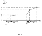
- FIG. 2 illustrates only one of many possible timing scenarios for the
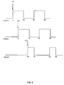
circuit 100. Upon the occurrence of edge Cl, S propagates from points A to C to D. The signal S is blocked at D (the input of the latch 107) until such time as the edge C2 occurs, at which point S propagates to point F and on to point G. Other timing scenarios are also possible. For example, depending upon the timing relationship between edges C1 and C2, the signal S may not be blocked at point D (the input of the latch 107), but may instead pass through thelatch 107 without being blocked for any period of time. When a signal is blocked at the input of a latch, it is a “red light” condition. When a signal reaches the input of a latch and propagates through without being blocked for any period of time, it is a “green light” condition. - FIG. 3 illustrates a possible timing relationship between the edges of three clock signals; Clock 1, Clock2, and Clock3. The signal Clock1 has a period of 20 and is high from the
time 0 to thetime 10. Signal Clock1 is then low fromtime 10 totime 20. The signal Clock2 also has a period of 20, but is high from atime 5 to atime 15, and low from 15 to 25. The signal Clock3 has a period of 20 and is high fromtimes 14 to 19, and low fromtimes 19 to 34. Given this timing relationship among the clock signals, it is possible to compute slack times for points in thecircuit 100 by assigning values to the various propagation delays of the elements. - Consider the situation where P 1=0, P2=2 nanoseconds, P3=0, and P4=3 nanoseconds. Assume that the timing of the circuit requires that occurrence of edge C1 corresponds with the occurrence of edge C3. That is, a signal S that is propagated from point A (the input of the source flip-flop 102) upon the occurrence of edge C1 at time t=0 and must arrive at point G (the input of the destination flip-flop 108) prior to the occurrence of the edge C3 at time t=14. For purposes of simplifying the present discussion, the setup times for the
latch 107 and the flip-flop 108 are ignored. At the occurrence of edge C1 (t=0), S begins to propagate downstream from A. Signal S can arrive at point D at any time prior or during the open interval of thelatch 107 at t=5 and t=15 and still make it to point G before the occurrence of edge C3. Between times t=5 and t=15, thelatch 107 is open and the signal S propagates through thelatch 107. In the present example, signal S arrives at point D at t=2 and hits a red light until the occurrence of edge C2 at time t=5. At the occurrence of edge C2, the signal S propagates through the latch and arrives at point G at time t=8. The slack time at point G is the difference between when S actually arrives at point G, and the latest time S could have arrived at point G and still met the timing of the circuit. Thus the slack time at point G is: - 14−8=6 nanoseconds.
- Working backwards it is possible to determine the slack times at other points in the circuit. The slack time at F is
- (14−3)−5=6
- The slack time at the clock terminal E of the
latch 107 is - (14−3)−5=6 nanoseconds (the CK-Q delay of the latch is assumed to be 0).
- The slack time at the input terminal D of the
latch 107 is - 15−2=13, for reasons set forth in the following description.
- A “path” is a set of related events at different points in a circuit. The points in a path are related by a common signal that passes through them without stopping. If a signal gets to a latch when it is closed, that path stops there. A new path starts at the enable pin when the latch opens. The slack time of a path is the slack time at the end of the path (the slack time as determined for the path at the final point in the path). Paths provide useful information about circuit timing behavior, including slack times at points in the circuit. To determine the slack times at points along a path, an event of interest is selected at the end point of the path. This event is referred to herein as the “final event of interest”. In the preceding example, the final event of interest is the occurrence of the edge C 3 at the flip-
flop 108. At the start of the path, an event of interest is determined corresponding to the final event of interest. This corresponding event of interest is referred to herein as the “starting event of interest”. In the preceding example, the starting event of interest is the occurrence of edge C1. For a specific path, the slack time will be the same at all the points. - Typically, the interval of time between the starting event of interest and the final event of interest bears upon the slack times at points along the path connecting the events. Thus, for events based upon periodic signals, it is important to examine all possible timing relationships between events comprised by the signals. In one embodiment, two periodic signals comprising the events of interest are “walked” in time to identify all possible relationships between the edges of the signals. For example, if the starting event of interest is a rising edge of a first clock signal, the first clock signal is traversed in time and each rising edge is examined against the corresponding (following most closely in time) rising edge of the second clock signal comprising the final event of interest. Each different timing relationship between the edges is recorded for purposes of determining slack times along the path between the events, when latches are involved. In a path without latches, only the timing relationship with the shortest time in between events is recorded, because that represents the worst slack time.
- Consider the pair of signal embodiments represented in FIG. 4. Both signals A and B are periodic. However, the signals have different periods, different duty cycles, and the edges of the signals are not coincident in time. Assume that there are no latches along the path to analyze. Choosing events (rising edges) C 1′ and C3′ alone as the starting and final events of interest does not produce a worst-case analysis of setup slack times along the path, because T2 (the difference in time between edge C1′ and edge C3′) is larger than both T1 (the difference in time between edge C1 and edge C3) and T3 (the difference in time between edge C1″ and edge C3″). Choosing events C1′ and C3′ alone is also insufficient because T1 is larger than T3. Choosing events C1″ and C3″ results in a slack time analysis that is worst-case of the three, because T3<T1<T2.
- A more complicated situation arises when, as in the
circuit embodiment 100 of FIG. 1, there are one ormore latches 107 along the path between the starting and final events of interest. In this situation, the timing of the open intervals of the intervening latches becomes a consideration when determining the worst-case slack time of the path. The situation in which the latch clock signal and the destination flip-flop clock signal are closest in time may not lead to the worst-case slack situation for the path. Rather, a “back propagation” of required times for each possible relationship among the clocks may be performed, from the final event of interest to the source event of interest. In other words, starting with the required time of the final event of interest, required times are determined at successive neighboring points upstream in the path to keep track of possible relationships among the clocks encountered thus far. - Consider the situation where the final event of interest is a rising (trigger) edge of Clock 3, the clock signal to the destination flip-
flop 108. The signal Clock3 is periodic. The rising edge selected as the final event of interest has a required time. During back propagation of this required time, thelatch 107 is encountered between points D and F in the path. Recall that thelatch 107 propagates the signal S from point D to point F during the interval when the latch clock signal, e.g. Clock2, is high. The required time for the signal S to reach point D (the D input terminal of the latch 107) occurs some time before the falling (closing) edge of Clock2 corresponding to the rising (trigger) edge of Clock3 that was selected as the final event of interest. A process known as “ping-pong” may be employed to identify an edge to reference this required time to. FIG. 5 illustrates the ping-pong process. At 502 the closest rising (opening) edge of Clock2 preceding the selected edge of Clock3 is selected (the ‘ping’). At 504 the falling (closing) edge of Clock2 following this opening edge is determined (the ‘pong’). - This process is illustrated in flow chart form in FIG. 6. At 602 the closest opening edge of the upstream signal preceding the edge of the downstream signal is selected. At 604 the closing edge of the upstream signal following this opening edge is determined. At 606 the earlier in time of the closing edge of the upstream signal and the edge of the downstream signal is chosen as the event of interest upon which the required time at a point is referenced.
- When there are multiple relationships between the edges of Clock 2 and Clock3, the two signals are walked using the process described previously in conjunction with FIG. 4. A required time is determined for the signal S at point D for each possible different relationship between a rising edge of Clock3 and a corresponding rising edge of Clock2. All of these required times are then propagated back along the path, along with a corresponding event to which they are referenced, until the source flip-
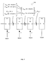
flop 102 is reached, or until another latch is encountered in the path. For each required time that is propagated back, the corresponding reference event is either the rising edge of Clock3 or the corresponding falling edge of Clock2, whichever is earlier in time. When a second latch is encountered in the path during back propagation of required times, the process described above is repeated. - With reference to FIG. 7, a
circuit embodiment 700 comprises a source flip-flop FF1 having a clock Clock1, a destination flip-flop FF2 having a clock Clock4, and two intervening latches L1 and L2 having clocks Clock2 and Clock3, respectively. To compute the worst-case slack time for the path from FF1 to FF2, a final event of interest is selected. Let us choose, for example, the edge E14 of Clock4. A signal S that arrives at point C must arrive before E14 arrives at the clock terminal of the flip-flop FF2 in order to be stored by the flip-flop FF2. The signal S must arrive at sufficient time before Clock4 to meet the setup time of the flip-flop FF2. To simplify the discussion, the setup times of the circuits will be overlooked, however, in practical applications the required times determined at each point in the circuit would reflect the setup times of the circuit elements. - The required time at C is recorded as T RC1, e.g. the required time for signal S at point C in the circuit. In practical applications, the setup time of the flip-flop FF2 is factored into TRC1, so that for example if the flip-flop FF2 has a 1 nanosecond setup time, TRC1 is −1, e.g. 1 nanosecond sooner than the arrival of C4. Working backward along the path, latch L2 is encountered. Latch L2 is clocked by signal Clock3. FIG. 8 shows signal embodiments illustrating possible relationships between Clock1, Clock2, Clock3, Clock4. Clock1 has a period of 30 and rising edges at 10, 40, 70, and 100. Clock1 has falling edges at 15, 45, 75, and 105. Clock2 has a period of 120, with four pulses per period, and rising edges at 15, 46, 76, and 104. Clock2 has falling edges at 22, 51, 83, and 113. Clock3 has a period of 60, with two pulses per period, and rising edges at 20, 52, 80, and 112. Clock3 has falling edges at 24, 57, 84, and 117. Clock4 has a period of 30 and rising edges at 25, 55, 85, and 115. Clock4 has falling edges at 28, 58, 88, and 118.
- Referring to the signals Clock 3 and Clock4, edge E9 of Clock3 corresponds to (is the closest preceding edge in time) edge E13 of Clock4. In other words, if edge E13 is used to clock the flip-flop FF2, then edge E9 is presumed to be the edge that will open the preceding latch L2. Edge E10 of Clock3 corresponds to edge E14 of Clock4. The other edges of Clock3 and Clock4 have the same relationship (e.g. the same relative timing) as edges E9/E13 and E10/E14. Thus, the signals Clock3 and Clock4 have two possible relationships. The “virtual period” of the two clock signals Clock4 and Clock3 is determined as the least common multiple of the clock periods of the two signals. In this case, the virtual period is 60.
- Referring back to FIG. 7, two required times are recorded for point B in the
circuit 700, one required time for each possible relationship between the signals Clock3 and Clock4. The required times at point B are determined using the D-Q propagation delay of the intervening latch. A first required time entry TRB1 is recorded for point B. Using the ping-pong approach, a reference event, in this case E9′, is associated with this required time relative to E13 (because required times are only significant in relation to some event). The interval <E9, E9′>is also associated with the required time and like the required time is made relative to the reference event (e.g. the start and stop times of the interval are each made relative to the time of the reference event E9′). The purpose of recording the latch open interval with the required time will be explained subsequently. - A second required time entry T RB2 is recorded for point B. Using the ping-pong approach, a reference event, in this case E14, is associated with this required time relative to E14. The interval <E10, E14>is also associated with the required time and like the required time is made relative to the reference event. The interval, as one will recall from FIG. 6, is <E10, E14>, not <E10, E10′>, because E14 occurs at 55 ns and E10′ occurs at 57 ns.
- The set of reference edges at a point in a path may be referred to as a “virtual clock edge list” at the point in the path.
- As the preceding example illustrates, in one embodiment of a method to determine slack times of a circuit, the reference event for required times at a point preceding a latch is a closing edge of the latch clock signal when the latch closes prior to the occurrence of the corresponding downstream event.
- Next, required times are determined for point A, based upon the required times determined for point B. The latch L 1 is clocked by signal Clock2. The edges of Clock2 have four possible relationships with the set of reference signals determined at point B. The required times associated with the reference edges E5′, E6′, E7′, and E8′ are the ones that would have been originally from edges E13, E14, E15, and E16 respectively. The virtual period of the signals comprising the reference edges at point B is 60. The required time TRB1 at point B is referenced to the edge E9′ of signal Clock3. A required time TRA1 at point A, corresponding to the required time TRB1 at point B, is determined by adjusting the required time TRB1 to be relative to the reference edge at point A. Edge E5′ is chosen as the reference edge at point A using the ping-pong approach. Thus if the required time TRB1 at E9′ is 1, the required time TRA1 at E5′ is 3, because E9′ occurs at 24, two nanoseconds later than E5′ at 22. An interval <E9,E5′>is associated with TRA1, representing the composite (overlap) of the latch open intervals <E9,E9′>and <E5,E5′>. (e.g. the overlap of the open intervals of all latches downstream from point A along the path). Actual delays in the circuit are taken into account in adjusting the latch open interval <E9,E9′>before finding the overlap with interval <E5,E5′>(this simplified example ignores the delays). Also, both of the intervals are made relative to the new reference edge E5′ before determining the overlap. The purpose of the composite open interval will be covered more fully in the determination of slack times.
- Likewise, a required time T RA2 is recorded at point A, corresponding to the required time TRB1 plus one virtual period of the signals comprising the reference edges at point B. One virtual period (60) was added to the reference edge E9′ to determine the corresponding reference edge E11′ from the next virtual period of Clock3. Using the ping-pong approach, the reference event is set to E7′. A composite open interval <E11,E7′>is associated with TRA2, representing the overlap of the latch open intervals <E11,E11′>and <E7,E7′>. Adjustments for circuit delay are made in the manner described above. The intervals are made relative to the same reference edge, as described above.
- The required time T RA3 at point A represents a third relationship between the edges of Clock2 and Clock3. Applying the ping-pong approach to the reference edge E14 for TRB2, the reference event for TRA3 is set to E6′. There is no interval of time during which the open intervals <E10,E10′>and <E6,E6′>overlap (assume for the purpose of this description that this is true, even after adjusting for circuit delay and making the intervals relative to E6′). Thus the composite open interval is set to undefined (!).
- A fourth required time T RA4 is recorded at point A, corresponding to the required time TRB3 plus one virtual period of the signals comprising the reference events at point B. Applying the ping-pong approach to edge E16 (E14 plus one virtual period), the reference event for TRA4 is determined to be E8′. A composite open interval <E12,E8′>is associated with TRA4, representing the overlap of the latch open intervals <E12,E12′>and <E8,E8′>. Again, circuit delays are ignored, and the intervals are made relative to E8′ in determining the overlap.
- Eventually, the source flip-flop FF 1 or other origination point of the path is reached. The signal Clock1 is the clock signal for flip-flop FF1. For each required time at point A, a corresponding arrival time is determined at point X, where Clock1 is received. Where the edges of the signal Clock1 have multiple relationships with the virtual clock edge list, a particular required time entry at point A may give rise to multiple arrival time entries at point X. Edges of Clock1 are chosen that immediately precede each of the required times. In this manner, each back propagated required time and event of interest is associated with a source event of interest at the starting point of the path. Each required time is associated with one or more starting events of interest. If the number of starting events of interest is greater than one, then the relationship of one or more virtual periods is different with respect to the source clock.
- The source events of interest identified in this fashion may then be propagated downstream along the path. Any uncertainty in the arrival time of a source event at point X is accounted for as an interval (T1, T2) of potential arrival times for the source event, where T1 is the earliest possible arrival time for the event, and T2 is the latest possible arrival time for the event.
- Arrival times for the source events of interest at various points downstream are determined by adding propagation delays of the elements encountered by the events as they propagate downstream. Each element can have a minimum and maximum propagation delay. The arrival ranges are “widened” according to the maximum propagation delay of the elements encountered. To widen a range, T1 is increased by the minimum propagation delay of the element, and T2 is increased by the maximum propagation delay of the element.
- When a latch is encountered during propagation of arrival times downstream, entries may be merged to determine the arrival time entries at the next downstream point after the latch. Referring to FIG. 9, at point A there are four arrival time entries, each corresponding to a required time entry from FIG. 7. The arrival time entry (T1 AA1, T2AA1, E5′) corresponds to the required time entry (TRA1, E5′, <E9,E5′>); the arrival time entry (T1AA2, T2AA2, E7′) corresponds to the required time entry (TRA2, C4′, <E11,E7′>); and so on. Upon encountering a latch during propagation downstream, arrival time entries corresponding to required time entries with a common parent are merged to create an arrival time entry at the next downstream point after the latch. Thus the two arrival time entries (T1AA1, T2AA1, E5′) and (T1AA2, T2AA2, E7′) at point A are merged to create the arrival time entry at point B, (T1AB1, T2AB1, E9′). The value T1AB1 is determined as the minimum of T1AA1 and T1AA2. The value T2AB1 is determined as the maximum of T2AA1 and T2AA2. Before merging, the arrival time intervals are made relative to (referenced to) the reference event of the corresponding parent event. Thus, the values T1AB1 and T2AB1 are adjusted so that they are relative to edge E9′ before performing the merge. Making the times relative to E9′ involves an adjustment (in the case of arrival times T1AA1 and T2AA1 relative to E5′, adding or subtracting the difference between E5′ and E9′) and a translation (in the case of the arrival times T1AA2 and T2AA2 relative to E7′, making them relative to E11′). Thus the arrival range relative to E9′ represents the range of all possible arrivals that could arrive relative to E9′ or any clock edge related to E9′ by the virtual clock period at point B.
- The interval (T1 AB1, T2AB1) is widened according to the minimum and maximum propagation delays of the latch L1. The interval (T1AB1, T2AB1) is “clipped” according to the relevant open interval of the latch L1. Clipping involves finding the overlap of the two intervals. When the reference event is edge E9′, the corresponding open interval of latch L1 is <E5,E5′>. When the reference event is edge E14, the corresponding open interval of latch L1 is <E6,E6′>.
- Likewise, the two arrival time entries (T1 AA3, T2AA3, E6′) and (T1AA4, T2AA4, E8′) at point A are merged and adjusted to create the arrival time entry at point B, (T1AB2, T2AB2, E14).
- A situation may arise where the arrival interval and the open interval of the latch do not overlap. If the arrival interval ends before the open interval begins, the signal S always hits a red light at the latch. In this case, the path from point X is ended at point A, and a new path is started from point Y. The source events of interest for this new path are the edges of the clock signal Clock 2.
- If the arrival interval begins before the open interval begins, but ends during or after the open interval, the signal S may hit a red light at the latch. In this case, the path from point X is ended at point A, and an identical path from point X is continued on through the latch (using the CK-Q propagation delay of the latch). Another path is started from point Y. The source events of interest for this new path are the edges of the clock signal Clock 2. Slack times for the path ending at A are determined relative to the closing edge of the latch clock, providing a slack value that is relevant for the path up to that latch but not beyond.
- In one embodiment, arrival entries will be recorded at X only for those edges of Clock 2 resulting in red-light conditions at point A. For example, if there are 6 different clock relationships between the latch clock and the clocks comprising the reference events at a latch, if only on the fifth relationship involves a red-light situation, then an arrival entry and a path from the latch clock terminal to the latch output terminal will be produced only for that fifth relationship. In other words, for each reference event at the data terminal of a latch, a decision is made as to whether or not to begin a new path at the clock terminal of the latch. If an arrival entry gives rise to a red light situation, paths are started from the clock terminal of the latch and proceeding downstream through the design for each arrival at the latch clock terminal that gives rise to a red light situation. Other arrivals at the clock terminal do not give rise to new paths.
- A “period offset” may be included with the arrival entries. The period offset associated with an arrival entry indicates which period of the virtual clock for the reference event comprised by the arrival entry had the earliest arrival time. When arrival entries are merged into a parent entry upon crossing a latch, the period offset indicates from which virtual period of the reference event the red-light situation arose. The period offset is increased appropriately when merging arrival entries. When a path is started at a latch clock terminal, the period offsets there are set based on the period offsets of the arrival entries at the latch data terminal that gave rise to the red light condition. The period offset is used when a path is started at the clock pin of a latch to begin the path an appropriate number of iterations of the virtual period out to correspond with the red light arrival.
- When the arrival interval falls completely within the open interval of the latch, the path from point X is ended at point A, and an identical path from point X is continued on through the latch (using the D-Q propagation delay of the latch).
- If the arrival interval begins after the open interval ends, the signal S never gets through the latch on time to meet the timing requirements of the circuit. In this case, the path from point X is ended at point A, and the timing failure is recorded.
- In this case a new path may be started at the output terminal of the latch. The circuit designer may examine this path to ascertain what would be the worst case slack from the latch output terminal to the final event of interest.
- In one embodiment, each arrival entry may also comprise a minimum late value and a maximum early value. These values may be applied to ascertain when to start a path at the latch clock terminal or the latch output terminal in situations where multiple signals merge coming to the input terminal of the latch.
- Returning to the example of FIG. 9, the two arrival time entries at point B are merged to create the arrival time entry at point C, (T1 AC1, T2AC1). The interval (T1AC1, T2AC1) is widened according to the minimum and maximum propagation delays of the latch L2. The interval (T1AC1, T2AC1) is “clipped” according to the relative open interval of the latch L2. Paths are terminated at point B, and new paths created, according to the same process specified for point A.
- Another situation that can occur is where two or more paths merge at a circuit element. Referring to FIG. 10, a
circuit element 1050 has two inputs having points A and B, respectively. Signals S1 and S2 arrive at points A and B, respectively. Arrival intervals (T1A, T2A) and (T1B, T2B) are determined for signals S1 and S2 at points A and B, respectively. One of these intervals is referenced to the reference event of the other, each interval is adjusted for the corresponding propagation delay through the element 1050 (A to C delay and B to C delay), and then the two intervals are merged to produce the arrival interval (T1c, T2c) at point C. - Referring to FIG. 11, signals S 1 and S2 each have a best-case and worst-case slew time. Assuming that a signal transition is complete when the signal crosses the midpoint of its low-high range, then the rising edge of signal S1 occurs, in the worst case, at time t1 and in the best case at time t2. The rising edge of signal S2 occurs, in the best case, at time t3 and in the worst case at time t4. To merge the arrival intervals of these two signals, the delay range from A to C is calculated using the best and worst case slews for signal S1. The delay range from B to C is calculated using the best and worst case slews for signal S2. The two delay ranges are merged to determine the arrival ranges of the signal at C. The slew range of the merged signal is set to the worst-case slew of signal S1 (which is worse than the worst case slew of signal S2).
- Once required and arrival times are determined for all paths through the circuit, a list of paths having the worst-case slack times for a given point may be reported. FIG. 12 shows a
method embodiment 1200 for reporting paths with worse-case slack time in a circuit. At 1202 the starting points for all paths through a circuit are added to a priority path queue. A priority queue is an ordered collection. A particular point may be the starting point for multiple paths. A starting point may comprise multiple sets of required and arrival times determined according to the preceding analysis. Starting points are added for the rising and falling edges of the signal to trace through the design. - At 1204 slack times are determined at each starting point according to the required time and arrival time entries. When a path is started, an arrival time for each possible clock relationship is carried from the source clock all the way through the pipeline of latches. Each of these arrivals is updated appropriately as the path is extended. Each arrival can be compared with a required time at the current end point of the path by an appropriate adjustment. By examining each arrival as it passes through a latch, it can be determined whether or not the late value will pass through the latch. If so, the path continues. If not, the path is left undefined. The worst-case of the slack times determined in this fashion is the slack time of the path.
- Once slack times for all points are determined, the queue is ordered at 1206 according to slack time. Alternatively, the queue could be “self-ordering”, so that as paths are added, the queue reorders itself so that it is always ordered according to the slack time of its constituent paths. The path with the lowest (worst-case) slack time is placed at the head of the queue. The slack time of paths increases from the head of the path queue to the tail of the path queue.
- At 1208 the path at the head of the path queue (the path having the worst slack time) is removed from the path queue. A check is made to determine if this path is a complete path, e.g. if it has been extended to its ending point. If so, the path is “reported” by moving it to the report queue at 1210. This report queue is provided to the circuit designer and is self-ordering; that is, the first path moved to the report queue has the worst slack, the next path moved to the report queue has the second worst slack, and so on. Processing may stop once a number of worst case slack paths, as specified by the circuit designer, are reported.
- If, at 1214, extending a path would result in “fan out”, the path is cloned at 1216 to create one or more new paths proportional to the amount of fan-out. FIG. 13 shows an example of a fan out situation. A
circuit element 1302 has a single input and two outputs. When a path is extended from point A, a fan out occurs so that the output signal of thecircuit 1302 is provided at both points B and C. In this situation, the path is cloned (the path information is duplicated) to create one new, identical path. The existing path is extended from point A to point B, and the new path is extended from A and C. At 1218 slack times are computed at the end points of the paths and the paths are inserted into the path queue at the proper location, e.g. placed such that the ordering of the queue is maintained. - As paths are extended, the arrival ranges are adjusted according to the actual slew times of the signals. At the data terminal of a latch, each arrival range is examined to determine if the latest arrival time for the range falls within the open interval of the latch. If it does, the path is extended though the latch. Otherwise, the path is left undefined.
- Referring again to FIG. 12, the method then returns to 1208 to repeat, as long as the path queue is not empty, until a predetermined number of completed paths are removed to the report queue. This provides the circuit designer with a predetermined number of worst-case slack paths through the circuit.
- With reference to FIG. 14, information comprising a circuit design may be communicated from a
client device 1402 to aserver device 1404 via anetwork 1406. Thenetwork 1406 may comprise various technologies, including switches, routers, and computers of the Internet, the public phone network, and private collections of computers (so-called “intranets”). Optical, electrical, and wireless communication technologies may be employed, among other things. Theclient 1402 may be any processing device capable of storing and communicating information, such as a desktop computer, workstation, laptop computer, handheld computer, and so on. Theserver 1404 is any device comprising a process and memory that provides processing and/or data in response to requests from theclient 1402. Often, theserver 1404 is some form of powerful computer system. Theserver 1404 may perform processing on the circuit information provided by theclient 1402 and may communicate a resulting slack analysis to theclient 1402. - With reference to FIG. 15, an
apparatus embodiment 1500 for practicing embodiments of the present invention comprises a processing unit 1502 (e.g., a processor, microprocessor, micro-controller, etc.) and machine-readable media 1504. The apparatus may is an embodiment of a “computer system”, although in general a computer system can be any device comprising a processor and a memory, the memory to store instructions to supply to the processor for execution. Depending on the configuration and application (mobile, desktop, server, etc.), thememory 1504 may be volatile (such as RAM), non-volatile (such as ROM, flash memory, etc.) or some combination of the two. By way of example, and not limitation, the machinereadable media 1504 may comprise volatile and/or nonvolatile media, removable and/or non-removable media, including: RAM, ROM, EEPROM, flash memory or other memory technology, CD-ROM, digital versatile disks (DVD) or other optical storage, magnetic cassettes, magnetic tape, magnetic disk storage or other magnetic storage devices, or any other medium which can be used to store the desired information to be accessed by theapparatus 1500. The machinereadable media 1504 may be implemented in any method or technology for storage of information such as computer readable instructions, data structures, program modules or other data. Such instructions and data may, when executed by theprocessor 1502, carry out embodiments of methods in accordance with the present invention. - The
apparatus 1500 may comprise additional storage (removable 1506 and/or non-removable 1507) such as magnetic or optical disks or tape. Theapparatus 1500 may further compriseinput devices 1510 such as a keyboard, pointing device, microphone, etc., and/oroutput devices 1512 such as display, speaker, and printer. Theapparatus 1500 may also typically include network connections 1520 (such as a network adapter) for coupling to other devices, computers, networks, servers, etc. using either wired or wireless signaling media. - The components of the device may be embodied in a distributed computing system. For example, a terminal device may incorporate input and output devices to present only the user interface, whereas processing component of the system are resident elsewhere. Likewise, processing functionality may be distributed across a plurality of processors.
- The apparatus may generate and receive machine readable instructions, data structures, program modules or other data in a modulated data signal such as a carrier wave or other transport mechanism. The term “modulated data signal” means a signal that has one or more of its characteristics set or changed in such a manner as to encode information in the signal. This can include both digital, analog, and optical signals. By way of example, and not limitation, communication media includes wired media such as a wired network or direct-wired connection, and wireless media such as acoustic, RF, infrared and other wireless media. Communications media, including combinations of any of the above, should be understood as within the scope of machine readable media.
- Particular embodiments of a method and apparatus to perform slack analysis on a circuit design have been described herein. Many alternative embodiments will now become apparent to those skilled in the art. It should be recognized that the described embodiments are illustrative only and should not be taken as limiting in scope. Rather, the present invention encompasses all such embodiments as may come within the scope and spirit of the following claims and equivalents thereto.
Claims (33)
Priority Applications (1)
| Application Number | Priority Date | Filing Date | Title |
|---|---|---|---|
| US10/319,018 US7062734B2 (en) | 2002-04-05 | 2002-12-12 | Slack time analysis through latches on a circuit design |
Applications Claiming Priority (2)
| Application Number | Priority Date | Filing Date | Title |
|---|---|---|---|
| US37080502P | 2002-04-05 | 2002-04-05 | |
| US10/319,018 US7062734B2 (en) | 2002-04-05 | 2002-12-12 | Slack time analysis through latches on a circuit design |
Publications (2)
| Publication Number | Publication Date |
|---|---|
| US20030192020A1 true US20030192020A1 (en) | 2003-10-09 |
| US7062734B2 US7062734B2 (en) | 2006-06-13 |
Family
ID=28678107
Family Applications (1)
| Application Number | Title | Priority Date | Filing Date |
|---|---|---|---|
| US10/319,018 Expired - Lifetime US7062734B2 (en) | 2002-04-05 | 2002-12-12 | Slack time analysis through latches on a circuit design |
Country Status (1)
| Country | Link |
|---|---|
| US (1) | US7062734B2 (en) |
Cited By (9)
| Publication number | Priority date | Publication date | Assignee | Title |
|---|---|---|---|---|
| US20040078183A1 (en) * | 2002-10-21 | 2004-04-22 | Victor Drabkin | System and method of system response testing and modeling |
| US20040133866A1 (en) * | 2003-01-03 | 2004-07-08 | Hyeonjoon Shim | Clock edge value calculation in hardware simulation |
| WO2004025706A3 (en) * | 2002-09-13 | 2004-07-15 | Cadence Design Systems Inc | Automatic insertion of clocked elements into an electronic design to improve system performance |
| US20060010411A1 (en) * | 2004-07-12 | 2006-01-12 | International Business Machines Corporation | Method for netlist path characteristics extraction |
| US20060101361A1 (en) * | 2004-11-03 | 2006-05-11 | International Business Machines Corporation | Slack sensitivity to parameter variation based timing analysis |
| US7206958B1 (en) * | 2003-10-21 | 2007-04-17 | Sun Microsystems, Inc. | Determining cycle adjustments for static timing analysis of multifrequency circuits |
| US20120065955A1 (en) * | 2010-09-15 | 2012-03-15 | Qualcomm Incorporated | Modeling Output Delay of a Clocked Storage Element(s) |
| US20160266604A1 (en) * | 2015-03-09 | 2016-09-15 | Apple Inc. | Multi-bit flip-flop reorganization techniques |
| US12147745B2 (en) * | 2018-09-25 | 2024-11-19 | The Boeing Company | Engineering analysis of a structural product |
Families Citing this family (4)
| Publication number | Priority date | Publication date | Assignee | Title |
|---|---|---|---|---|
| US7239996B2 (en) * | 2002-06-10 | 2007-07-03 | Boland Arthur J | Causality based event driven timing analysis engine |
| US20070089076A1 (en) * | 2005-10-14 | 2007-04-19 | Sun Microsystems, Inc. | Application of consistent cycle context for related setup and hold tests for static timing analysis |
| US7873953B1 (en) | 2006-01-20 | 2011-01-18 | Altera Corporation | High-level language code sequence optimization for implementing programmable chip designs |
| US10216875B2 (en) | 2017-02-23 | 2019-02-26 | International Business Machines Corporation | Leverage cycle stealing within optimization flows |
Citations (16)
| Publication number | Priority date | Publication date | Assignee | Title |
|---|---|---|---|---|
| US4763289A (en) * | 1985-12-31 | 1988-08-09 | International Business Machines Corporation | Method for the modeling and fault simulation of complementary metal oxide semiconductor circuits |
| US5218551A (en) * | 1990-04-30 | 1993-06-08 | International Business Machines Corporation | Timing driven placement |
| US5365463A (en) * | 1990-12-21 | 1994-11-15 | International Business Machines Corporation | Method for evaluating the timing of digital machines with statistical variability in their delays |
| US5404360A (en) * | 1991-08-30 | 1995-04-04 | Mitsubishi Denki Kabushiki Kaisha | Simulator for simulating circuit operation |
| US5740347A (en) * | 1995-05-01 | 1998-04-14 | Synopsys, Inc. | Circuit analyzer of black, gray and transparent elements |
| US5790830A (en) * | 1995-12-29 | 1998-08-04 | Synopsys, Incorporated | Extracting accurate and efficient timing models of latch-based designs |
| US5864487A (en) * | 1996-11-19 | 1999-01-26 | Unisys Corporation | Method and apparatus for identifying gated clocks within a circuit design using a standard optimization tool |
| US5894419A (en) * | 1997-04-21 | 1999-04-13 | International Business Machines Corporation | System and method for robust clocking schemes for logic circuits |
| US6185723B1 (en) * | 1996-11-27 | 2001-02-06 | International Business Machines Corporation | Method for performing timing analysis of a clock-shaping circuit |
| US6401231B1 (en) * | 1997-04-25 | 2002-06-04 | Cadence Design Systems, Inc. | Method and apparatus for performing both negative and positive slack time budgeting and for determining a definite required constraint during integrated circuit design |
| US6438731B1 (en) * | 1999-09-13 | 2002-08-20 | Synopsys, Inc. | Integrated circuit models having associated timing exception information therewith for use in circuit design optimizations |
| US6442739B1 (en) * | 1998-05-01 | 2002-08-27 | Cadence Design Systems, Inc. | System and method for timing abstraction of digital logic circuits |
| US6496972B1 (en) * | 1999-09-13 | 2002-12-17 | Synopsys, Inc. | Method and system for circuit design top level and block optimization |
| US6604227B1 (en) * | 2001-08-10 | 2003-08-05 | Hewlett-Packard Development Company, L.P. | Minimal level sensitive timing abstraction model capable of being used in general static timing analysis tools |
| US6611948B1 (en) * | 2001-08-10 | 2003-08-26 | Hewlett-Packard Development Company, L.P. | Modeling circuit environmental sensitivity of a minimal level sensitive timing abstraction model |
| US6678644B1 (en) * | 1999-09-13 | 2004-01-13 | Synopsys, Inc. | Integrated circuit models having associated timing exception information therewith for use with electronic design automation |
-
2002
- 2002-12-12 US US10/319,018 patent/US7062734B2/en not_active Expired - Lifetime
Patent Citations (17)
| Publication number | Priority date | Publication date | Assignee | Title |
|---|---|---|---|---|
| US4763289A (en) * | 1985-12-31 | 1988-08-09 | International Business Machines Corporation | Method for the modeling and fault simulation of complementary metal oxide semiconductor circuits |
| US5218551A (en) * | 1990-04-30 | 1993-06-08 | International Business Machines Corporation | Timing driven placement |
| US5365463A (en) * | 1990-12-21 | 1994-11-15 | International Business Machines Corporation | Method for evaluating the timing of digital machines with statistical variability in their delays |
| US5404360A (en) * | 1991-08-30 | 1995-04-04 | Mitsubishi Denki Kabushiki Kaisha | Simulator for simulating circuit operation |
| US6158022A (en) * | 1995-05-01 | 2000-12-05 | Synopsys, Inc. | Circuit analyzer of black, gray and transparent elements |
| US5740347A (en) * | 1995-05-01 | 1998-04-14 | Synopsys, Inc. | Circuit analyzer of black, gray and transparent elements |
| US5790830A (en) * | 1995-12-29 | 1998-08-04 | Synopsys, Incorporated | Extracting accurate and efficient timing models of latch-based designs |
| US5864487A (en) * | 1996-11-19 | 1999-01-26 | Unisys Corporation | Method and apparatus for identifying gated clocks within a circuit design using a standard optimization tool |
| US6185723B1 (en) * | 1996-11-27 | 2001-02-06 | International Business Machines Corporation | Method for performing timing analysis of a clock-shaping circuit |
| US5894419A (en) * | 1997-04-21 | 1999-04-13 | International Business Machines Corporation | System and method for robust clocking schemes for logic circuits |
| US6401231B1 (en) * | 1997-04-25 | 2002-06-04 | Cadence Design Systems, Inc. | Method and apparatus for performing both negative and positive slack time budgeting and for determining a definite required constraint during integrated circuit design |
| US6442739B1 (en) * | 1998-05-01 | 2002-08-27 | Cadence Design Systems, Inc. | System and method for timing abstraction of digital logic circuits |
| US6438731B1 (en) * | 1999-09-13 | 2002-08-20 | Synopsys, Inc. | Integrated circuit models having associated timing exception information therewith for use in circuit design optimizations |
| US6496972B1 (en) * | 1999-09-13 | 2002-12-17 | Synopsys, Inc. | Method and system for circuit design top level and block optimization |
| US6678644B1 (en) * | 1999-09-13 | 2004-01-13 | Synopsys, Inc. | Integrated circuit models having associated timing exception information therewith for use with electronic design automation |
| US6604227B1 (en) * | 2001-08-10 | 2003-08-05 | Hewlett-Packard Development Company, L.P. | Minimal level sensitive timing abstraction model capable of being used in general static timing analysis tools |
| US6611948B1 (en) * | 2001-08-10 | 2003-08-26 | Hewlett-Packard Development Company, L.P. | Modeling circuit environmental sensitivity of a minimal level sensitive timing abstraction model |
Cited By (20)
| Publication number | Priority date | Publication date | Assignee | Title |
|---|---|---|---|---|
| WO2004025706A3 (en) * | 2002-09-13 | 2004-07-15 | Cadence Design Systems Inc | Automatic insertion of clocked elements into an electronic design to improve system performance |
| US20040158806A1 (en) * | 2002-09-13 | 2004-08-12 | Scheffer Louis K. | Automatic insertion of clocked elements into an electronic design to improve system performance |
| US7207024B2 (en) | 2002-09-13 | 2007-04-17 | Cadence Design Sytems, Inc. | Automatic insertion of clocked elements into an electronic design to improve system performance |
| US20040078183A1 (en) * | 2002-10-21 | 2004-04-22 | Victor Drabkin | System and method of system response testing and modeling |
| US20040133866A1 (en) * | 2003-01-03 | 2004-07-08 | Hyeonjoon Shim | Clock edge value calculation in hardware simulation |
| US7062735B2 (en) * | 2003-01-03 | 2006-06-13 | Sun Microsystems, Inc. | Clock edge value calculation in hardware simulation |
| US7206958B1 (en) * | 2003-10-21 | 2007-04-17 | Sun Microsystems, Inc. | Determining cycle adjustments for static timing analysis of multifrequency circuits |
| US7290233B2 (en) * | 2004-07-12 | 2007-10-30 | International Business Machines Corporation | Method for netlist path characteristics extraction |
| US20060010411A1 (en) * | 2004-07-12 | 2006-01-12 | International Business Machines Corporation | Method for netlist path characteristics extraction |
| US20080052656A1 (en) * | 2004-11-03 | 2008-02-28 | Foreman Eric A | Slack sensitivity to parameter variation based timing analysis |
| US20060101361A1 (en) * | 2004-11-03 | 2006-05-11 | International Business Machines Corporation | Slack sensitivity to parameter variation based timing analysis |
| US7401307B2 (en) | 2004-11-03 | 2008-07-15 | International Business Machines Corporation | Slack sensitivity to parameter variation based timing analysis |
| US20080216036A1 (en) * | 2004-11-03 | 2008-09-04 | Foreman Eric A | Slack sensitivity to parameter variation based timing analysis |
| US7716616B2 (en) | 2004-11-03 | 2010-05-11 | International Business Machines Corporation | Slack sensitivity to parameter variation based timing analysis |
| US7870525B2 (en) | 2004-11-03 | 2011-01-11 | International Business Machines Corporation | Slack sensitivity to parameter variation based timing analysis |
| US20120065955A1 (en) * | 2010-09-15 | 2012-03-15 | Qualcomm Incorporated | Modeling Output Delay of a Clocked Storage Element(s) |
| US8886511B2 (en) * | 2010-09-15 | 2014-11-11 | Qualcomm Incorporated | Modeling output delay of a clocked storage element(s) |
| US20160266604A1 (en) * | 2015-03-09 | 2016-09-15 | Apple Inc. | Multi-bit flip-flop reorganization techniques |
| US9513658B2 (en) * | 2015-03-09 | 2016-12-06 | Apple Inc. | Multi-bit flip-flop reorganization techniques |
| US12147745B2 (en) * | 2018-09-25 | 2024-11-19 | The Boeing Company | Engineering analysis of a structural product |
Also Published As
| Publication number | Publication date |
|---|---|
| US7062734B2 (en) | 2006-06-13 |
Similar Documents
| Publication | Publication Date | Title |
|---|---|---|
| US7062734B2 (en) | Slack time analysis through latches on a circuit design | |
| US10776547B1 (en) | Infinite-depth path-based analysis of operational timing for circuit design | |
| US9223916B2 (en) | Timing analysis of asynchronous clock domain crossings | |
| US20150161315A1 (en) | Verification of asynchronous clock domain crossings | |
| US6799308B2 (en) | Timing analysis of latch-controlled digital circuits with detailed clock skew analysis | |
| US9690899B2 (en) | Prioritized path tracing in statistical timing analysis of integrated circuits | |
| JPH0812675B2 (en) | Digital machine performance simulation method and apparatus | |
| US7886246B2 (en) | Methods for identifying failing timing requirements in a digital design | |
| US9280624B2 (en) | System and method for efficient statistical timing analysis of cycle time independent tests | |
| US7873926B2 (en) | Methods for practical worst test definition and debug during block based statistical static timing analysis | |
| US9767239B1 (en) | Timing optimization driven by statistical sensitivites | |
| CN114548006B (en) | Integrated circuit verification method, device, electronic device, and storage medium | |
| US20070089076A1 (en) | Application of consistent cycle context for related setup and hold tests for static timing analysis | |
| US7134062B2 (en) | Static timing analysis approach for multi-clock domain designs | |
| US7155692B2 (en) | Method and system for performing timing analysis on a circuit | |
| US8024696B1 (en) | Clock speed for a digital circuit | |
| US10671790B2 (en) | Method and apparatus for verifying structural correctness in retimed circuits | |
| Georgakidis et al. | Towards a comprehensive SET analysis flow for VLSI circuits using static timing analysis | |
| US20060247906A1 (en) | Method for estimating clock jitter for static timing measurements of modeled circuits | |
| US6760894B1 (en) | Method and mechanism for performing improved timing analysis on virtual component blocks | |
| Devadas et al. | Event suppression: Improving the efficiency of timing simulation for synchronous digital circuits | |
| US7840925B1 (en) | Source specific timing checks on synchronous elements using a static timing analysis engine | |
| Öhlinger et al. | A digital delay model supporting large adversarial delay variations | |
| US20030212972A1 (en) | Unconventional clocked circuit components having multiple timing models | |
| US7983891B1 (en) | Receiver dependent selection of a worst-case timing event for static timing analysis |
Legal Events
| Date | Code | Title | Description |
|---|---|---|---|
| AS | Assignment |
Owner name: MENTOR GRAPHICS CORPORATION, OREGON Free format text: ASSIGNMENT OF ASSIGNORS INTEREST;ASSIGNOR:COLLINS, TRUMAN WESLEY JR.;REEL/FRAME:013585/0464 Effective date: 20021127 |
|
| STCF | Information on status: patent grant |
Free format text: PATENTED CASE |
|
| FPAY | Fee payment |
Year of fee payment: 4 |
|
| FEPP | Fee payment procedure |
Free format text: PAYOR NUMBER ASSIGNED (ORIGINAL EVENT CODE: ASPN); ENTITY STATUS OF PATENT OWNER: LARGE ENTITY |
|
| CC | Certificate of correction | ||
| FPAY | Fee payment |
Year of fee payment: 8 |
|
| MAFP | Maintenance fee payment |
Free format text: PAYMENT OF MAINTENANCE FEE, 12TH YEAR, LARGE ENTITY (ORIGINAL EVENT CODE: M1553) Year of fee payment: 12 |
|
| AS | Assignment |
Owner name: SIEMENS INDUSTRY SOFTWARE INC., TEXAS Free format text: MERGER AND CHANGE OF NAME;ASSIGNORS:MENTOR GRAPHICS CORPORATION;SIEMENS INDUSTRY SOFTWARE INC.;REEL/FRAME:055468/0023 Effective date: 20201230 |