US20030192012A1 - System and method to determine impact of line end shortening - Google Patents
System and method to determine impact of line end shortening Download PDFInfo
- Publication number
- US20030192012A1 US20030192012A1 US10/116,661 US11666102A US2003192012A1 US 20030192012 A1 US20030192012 A1 US 20030192012A1 US 11666102 A US11666102 A US 11666102A US 2003192012 A1 US2003192012 A1 US 2003192012A1
- Authority
- US
- United States
- Prior art keywords
- gate
- location
- critical dimension
- layout
- line end
- Prior art date
- Legal status (The legal status is an assumption and is not a legal conclusion. Google has not performed a legal analysis and makes no representation as to the accuracy of the status listed.)
- Granted
Links
Images


Classifications
-
- G—PHYSICS
- G06—COMPUTING OR CALCULATING; COUNTING
- G06F—ELECTRIC DIGITAL DATA PROCESSING
- G06F30/00—Computer-aided design [CAD]
- G06F30/30—Circuit design
- G06F30/39—Circuit design at the physical level
- G06F30/398—Design verification or optimisation, e.g. using design rule check [DRC], layout versus schematics [LVS] or finite element methods [FEM]
Definitions
- the invention relates to analyzing printed image distortion, and in particular to a system and method of determining the impact of line end shortening in the production of integrated circuits.
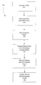
- FIG. 1A illustrates a standard layout structure 100 for forming a transistor.
- layout structure 100 includes a gate 101 and two diffusion areas 102 , which form the source and drain of the transistor.
- a first portion of gate 101 that extends past diffusion areas 102 and then terminates without connection is defined as an endcap margin 103
- a second portion of gate 101 that extends past diffusion areas 102 and connects to other structures is defined as a fieldcap margin 104 .
- Line end shortening is line end shortening, wherein a feature is less than its nominal length when a feature on a mask (or reticle) is transferred to a wafer.
- Line end shortening can be caused by diffraction, imperfect mask patterns (i.e. line rounding), resist, other processing effects, and/or combinations of one or more effects.
- FIG. 1B illustrates that line end shortening of gate 101 can cause an ideal printed line end 106 , with endcap margin 103 , to transfer to a wafer as actual printed line end 105 . Note that actual endcap margin 107 of actual printed line end 105 is clearly less than endcap margin 103 . Note further that line end shortening has greater effect on certain portions of the line end.
- actual printed line end 105 also has rounded corners due to other optical effects.
- the impact of line end shortening is accentuated on the edges of gate 101 that will interface with diffusion areas 102 during operation of the transistor formed by gate 101 and diffusion areas 102 .
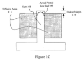
- the rounded corners of a gate can adversely impact transistor performance, as shown in FIG. 1C.
- an endcap margin 110 of a gate 108 is sufficiently small or the line end shortening is sufficiently great, then line end shortening (as indicated by actual printed line end 109 ) can decrease the flow of electrons between diffusion areas 111 when a predetermined voltage is applied to gate 108 (i.e. the transistor formed by gate 108 and diffusion areas 111 is turned “on”).
- the corner rounding of actual printed line end 109 reduces the area over which electrons can travel. This corner rounding can also cause leakage currents in the transistor, thereby resulting in a defective device.
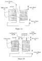
- FIG. 2A illustrates a method sometimes employed by wafer houses to measure the effect of line end shortening.
- the transistor formed by gate 101 and diffusion areas 102 (FIG. 1B) is shown relative to another transistor formed by a gate 101 ′ and diffusion areas 102 ′ (wherein these transistors substantially mirror each other).
- the spacing between line ends is measured.
- an ideal separation 201 can instead transfer to a wafer as an actual separation 202 .
- additional analysis is still required to determine the impact of the line end shortening.
- FIG. 2B illustrates two transistors: one transistor formed from gate 101 and diffusion areas 102 and another transistor formed from gate 108 and diffusion areas 107 .
- the measured distance between gates 101 and 108 i.e. ideal separation 201
- the measured distance between actual printed line ends 105 and 109 i.e. actual separation 202
- line end shortening can impact the functioning of the transistor formed by gate 108 and diffusion areas 107 , but not the transistor formed by gate 101 and diffusion areas 102 .
- an actual separation measurement cannot provide a reliable indication of the impact of line end shortening.
- a width (also called a critical dimension) of a feature can be measured to determine the impact of line end shortening.
- the critical dimension unlike measuring the separation between ends of two adjacent features, provides meaningful information regarding the impact of line end shortening. Moreover, unlike measuring the length of a shortened line end and its attendant inaccuracies due to rounded corners, the critical dimension can provide direct and accurate information that relates to device performance.
- obtaining this critical dimension can include determining a layout distance associated with the feature.
- the layout distance indicates a location on the feature associated with device performance. For example, if the feature is a gate, then the location can be associated with an edge of diffusion areas in the layout.
- device performance is related to a transistor formed by the gate and the diffusion areas.
- the location on the feature can indicate a portion of the gate over which electrons could flow during operation of the gate.
- the printing of evaluation points on the feature at the location can be simulated.
- the distance between these evaluation points can then be measured, wherein the distance is the critical dimension of the feature.
- the critical dimension is less than 10% of a desired critical dimension for the feature, then device performance can be impaired. This methodology can be repeated for other layout distances associated with the feature to provide further line end shortening impact information.
- a simulation report regarding one or more features on a layout can be provided. At least one feature on the layout is a line.
- the simulation report can include the critical dimension of the line, wherein the critical dimension indicates an impact of line end shortening on the line.
- the simulation report can further include a graphical output illustrating two deviation notches on the line (which correspond to the evaluation points), wherein the two deviation notches can be used to measure the critical dimension.
- the critical dimension is measured at a location on the line coincident with an edge of another feature on the layout.
- the line can be a gate and the other feature on the layout can be a diffusion area.
- the edge of the diffusion area can be a layout location with or without process deviation.
- FIG. 1A illustrates a transistor formed by a gate and two diffusion areas.
- FIG. 1B illustrates the effect of line end shortening on the gate shown in FIG. 1A.
- FIG. 1C illustrates the effect of line end shortening if the endcap margin is too small.
- FIG. 2A illustrates a known method of measuring line end shortening for two transistors.
- FIG. 2B illustrates how the method shown in FIG. 2A to measure line end shortening fails to accurately assess the impact of line end shortening.
- FIG. 3A illustrates one method of determining the impact of line end shortening.
- FIG. 3B illustrates a layout feature, wherein the critical dimension of the feature can determine the impact of line end shortening.
- FIG. 3C illustrates the layout feature of FIG. 3B assuming some process deviation.
- FIG. 3D illustrates another layout feature, wherein a process deviation margin can be used to position the line end shortening evaluation points.
- FIG. 4A illustrates an exemplary simulation output for a gate, wherein the simulation was performed using line end shortening evaluation points.
- FIG. 4B illustrates a prior art simulation output for a gate, wherein the simulation was performed using an evaluation point on a line end.
- a critical dimension of the feature can be measured to determine the impact of line end shortening.
- the critical dimension measurement advantageously provides accurate and meaningful information regarding device performance irrespective of endcap margin.
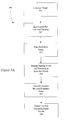
- FIG. 3A illustrates one exemplary methodology 390 for obtaining this critical dimension.
- a model can be constructed.
- the model can be developed based on the equipment, equipment settings, and other parameters used in the fabrication process.
- the model can be built by performing the fabrication process one or multiple times with test patterns, observing the actual features printed using these test patterns, and fitting a set of equations or matrix transformations that most nearly reproduce the locations of edges of features actually printed as output when the test pattern is provided as input.
- the ModelGenTM and/or ModelCalTM tools from Numerical Technologies, Inc. of San Jose, Calif., can be used to create suitable models.
- a model uses computational resources in proportion to the number of evaluation points where layout analysis is performed, e.g. approximately O(n) in the number of evaluation points. Specifically, to provide time efficient yet accurate results, the model can be run at selected points, i.e. the evaluation points, located on the edges of features, to determine the correction needed, if any, at each evaluation point to more closely approximate the desired design.
- step 392 the layout to be analyzed can be input into [TOOL?] for line end checking. After line ends are identified, certain evaluation points, called line end shortening evaluation points, can be placed on the features of the layout in step 393 .
- step 394 the printing of the line end shortening evaluation points can be simulated. Note that the process of using the model with the layout at the evaluation points is called a simulation (or a model if resist and optical effects are also computed).
- the distance between the simulated line end shortening evaluation points can be measured in step 395 , wherein the distance is the critical dimension.
- step 396 line end shortening impact results can be output.
- FIGS. 3 B- 3 D illustrate layouts including simplified features. These layouts also illustrate the line end shortening evaluation points that can be used to determine the critical dimension of those features. The placement (step 393 ) of these line end shortening evaluation points as well as their simulated printing (step 394 ) are described in reference to FIGS. 3 B- 3 D.
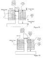
- FIG. 3B illustrates a layout including a transistor formed by a gate 301 and diffusion areas 302 .
- This transistor has an endcap margin 303 and a fieldcap margin 304 .
- a layout distance 312 can be provided, wherein layout distance 312 corresponds to the length of gate 301 at which the edges of diffusion areas 302 would theoretically cross gate 301 (corresponding to endcap margin 303 as opposed to fieldcap margin 304 ).
- Line end shortening evaluation points 311 can be positioned on opposite edges of the feature, i.e. gate 301 , at layout distance 312 .
- line end shortening evaluation points 311 can be used in a simulation to provide a critical dimension 310 of gate 301 at layout distance 312 .
- critical dimension 310 is the most appropriate dimension to consider the impact of line end shortening on gate 301 .
- the line end shortening of gate 301 can be accurately characterized as adversely affecting functionality (e.g. by decreasing the flow of electrons across diffusion regions 302 ).
- the deviation from this ideal critical dimension can accurately correlate to device performance.
- line end shortening evaluation points 311 may be positioned at a location that is not coincident with the edges of diffusion areas 302 .
- Process deviations could include, for example, diffusion area misalignment, an overlay error between gate and diffusion areas, and a gate narrowing error (which is a separate issue from necking, i.e. an problem resolved by critical dimension control). Any of these process deviations could cause a less than optimal positioning of line end shortening evaluation points 311 .
- FIG. 3C illustrates a diffusion misalignment error in which diffusion areas 302 could be slightly higher relative to gate 301 , thereby decreasing endcap margin 303 and increasing fieldcap margin 304 (see FIG. 3B). Specifically, endcap margin 303 could be reduced to endcap margin 305 and fieldcap margin 304 could be increased to fieldcap margin 306 .
- critical dimension 310 can still provide limited information regarding the impact on device performance, particularly if the line end shortening is significant. However, additional and/or alternative information can be generated to account for process deviations, thereby ensuring that the impact of line end shortening is fully analyzed.
- FIG. 3D illustrates another embodiment in which a critical dimension 326 of a gate 321 is measured at a predetermined distance away from diffusion areas 322 .
- a process deviation margin 324 can determine the position of line end shortening evaluation points 325 on gate 321 relative to a layout distance 323 .
- Process deviation margin 324 can be based on stepper accuracy, mask alignment accuracy, and/or dimension control of active regions. In one embodiment, process deviation margin 324 is approximately in the range of 20-30 nm.
- critical dimension 326 is less than the ideal critical dimension of gate 321 , then line end shortening has occurred. Moreover, this critical dimension 326 can accurately provide the impact of such line end shortening on the performance of the associated transistor. For example, in one embodiment, if critical dimension 326 is less than 10% the ideal critical dimension of gate 321 , then the transistor formed by gate 321 and diffusion areas 322 can be designated a defective transistor.
- a simulation tool such as the SiVL® tool licensed by Numerical Technologies, Inc., can determine layout distance 323 , process deviation margin 324 , the location of line end shortening evaluation points 325 , and critical dimension 326 as well as the target critical dimension and tolerance (i.e. the amount the critical dimension can acceptably vary).
- the simulation tool can assume typical process deviations to determine process deviation margin 324 or can also receive user/system input regarding specific process deviations based on the equipment, equipment settings, and other parameters to be used in the fabrication process.
- the simulation can provide a deviation (see step 306 of FIG. 3A), which indicates a printed edge location relative to a layout edge location.
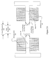
- FIG. 4A illustrates an exemplary calibrated output generated by a simulation tool.
- a simulation of a gate 401 having an evaluation point 404 could generate a report showing a deviation notch 405 , wherein the magnitude of deviation notch 405 indicates the location of the simulated printed edge corresponding to evaluation point 404 .
- deviation notch 405 can only provide indirect information regarding the impact of line end shortening. Therefore, in another embodiment, the simulation can advantageously generate supplemental information based on such calibrated output. For example, FIG.
- FIG. 4B illustrates the use of line end shortening evaluation points 402 to provide valuable supplemental information.
- a simulation of gate 401 having line end shortening evaluation points 402 could generate a report showing corresponding deviation notches 403 , wherein the distance between deviation notches 403 is the critical dimension of simulated printed gate 401 .
- a mask for fabricating an integrated circuit that accounts for line end shortening can have different gate lengths.
- at least one gate can have a length based on a set endcap margin, wherein the set endcap margin is determined by an impact of line end shortening on the gate. This length can be less than one based on a defined endcap margin provided by a design rule.
- an active region of at least one transistor of the IC can be positioned relative to a gate of that transistor based on the set endcap margin.
- the set endcap margin is less than the defined endcap margin provided by the design rule, the gate can still function properly during operation of the transistor.
- the gate has a critical dimension measured at an edge of the active region substantially equal to a target critical dimension. In another embodiment, the critical dimension is not substantially less than 10% of the target critical dimension.
- the simulation tool can also generate contours of printed features including the gates being simulated.
- the SiVL tool can operate in combination with another simulation tool licensed by Numerical Technologies, Inc., IC WorkbenchTM, to generate such aerial images.
- the aerial image view of the IC Workbench tool has the same functionality for local, small layout regions that are manually selected.
- the contours could illustrate line end shortening as well as other distortions of the printed features including proximity effects, line width variation (i.e. non-linearity), and corner rounding.
- the methods described herein can be applied to any lithographic process technology, including ultraviolet, deep ultraviolet (DUV), extreme ultraviolet (EUV), x-ray, and ebeam. Accordingly, it is intended that the scope of the invention be defined by the following claims and their equivalents.
Landscapes
- Engineering & Computer Science (AREA)
- Computer Hardware Design (AREA)
- Physics & Mathematics (AREA)
- Theoretical Computer Science (AREA)
- Evolutionary Computation (AREA)
- Geometry (AREA)
- General Engineering & Computer Science (AREA)
- General Physics & Mathematics (AREA)
- Design And Manufacture Of Integrated Circuits (AREA)
Abstract
Description
- 1. Field of the Invention
- The invention relates to analyzing printed image distortion, and in particular to a system and method of determining the impact of line end shortening in the production of integrated circuits.
- 2. Description of the Related Art
- FIG. 1A illustrates a
standard layout structure 100 for forming a transistor. Specifically,layout structure 100 includes agate 101 and twodiffusion areas 102, which form the source and drain of the transistor. A first portion ofgate 101 that extendspast diffusion areas 102 and then terminates without connection is defined as anendcap margin 103, whereas a second portion ofgate 101 that extendspast diffusion areas 102 and connects to other structures is defined as afieldcap margin 104. - One form of image distortion is line end shortening, wherein a feature is less than its nominal length when a feature on a mask (or reticle) is transferred to a wafer. Line end shortening can be caused by diffraction, imperfect mask patterns (i.e. line rounding), resist, other processing effects, and/or combinations of one or more effects. FIG. 1B illustrates that line end shortening of
gate 101 can cause an ideal printedline end 106, withendcap margin 103, to transfer to a wafer as actual printedline end 105. Note thatactual endcap margin 107 of actual printedline end 105 is clearly less thanendcap margin 103. Note further that line end shortening has greater effect on certain portions of the line end. Specifically, actual printedline end 105 also has rounded corners due to other optical effects. Thus, the impact of line end shortening is accentuated on the edges ofgate 101 that will interface withdiffusion areas 102 during operation of the transistor formed bygate 101 anddiffusion areas 102. - The rounded corners of a gate can adversely impact transistor performance, as shown in FIG. 1C. For example, if an
endcap margin 110 of agate 108 is sufficiently small or the line end shortening is sufficiently great, then line end shortening (as indicated by actual printed line end 109) can decrease the flow of electrons between diffusion areas 111 when a predetermined voltage is applied to gate 108 (i.e. the transistor formed bygate 108 and diffusion areas 111 is turned “on”). Specifically, the corner rounding of actual printedline end 109 reduces the area over which electrons can travel. This corner rounding can also cause leakage currents in the transistor, thereby resulting in a defective device. - To solve such problems associated with line end shortening, design rules have been used that recommend minimum endcap margins in the layout. However, due to corner rounding variations and the assumption of worst-case scenarios, this endcap margin can be undesirably long, thereby reducing the silicon area available for other circuits.
- FIG. 2A illustrates a method sometimes employed by wafer houses to measure the effect of line end shortening. For illustration purposes, the transistor formed by
gate 101 and diffusion areas 102 (FIG. 1B) is shown relative to another transistor formed by agate 101′ anddiffusion areas 102′ (wherein these transistors substantially mirror each other). In this method, instead of measuring the total length ofgates gates ideal separation 201 can instead transfer to a wafer as anactual separation 202. However, even ifactual separation 202 can be accurately determined, additional analysis is still required to determine the impact of the line end shortening. - Specifically, although
actual separation 202 in FIG. 2A can be acceptable (i.e. resulting in no defective devices), the identical separation in another configuration can result in one or more defective devices. For example, FIG. 2B illustrates two transistors: one transistor formed fromgate 101 anddiffusion areas 102 and another transistor formed fromgate 108 anddiffusion areas 107. Note that the measured distance betweengates 101 and 108 (i.e. ideal separation 201) and the measured distance between actual printed line ends 105 and 109 (i.e. actual separation 202) are identical to those in FIG. 2A. However, in FIG. 2B, line end shortening can impact the functioning of the transistor formed bygate 108 anddiffusion areas 107, but not the transistor formed bygate 101 anddiffusion areas 102. Thus, an actual separation measurement cannot provide a reliable indication of the impact of line end shortening. - Therefore, a need arises for a method of accurately determining the impact of line end shortening.
- In accordance with one aspect of the invention, a width (also called a critical dimension) of a feature can be measured to determine the impact of line end shortening. The critical dimension, unlike measuring the separation between ends of two adjacent features, provides meaningful information regarding the impact of line end shortening. Moreover, unlike measuring the length of a shortened line end and its attendant inaccuracies due to rounded corners, the critical dimension can provide direct and accurate information that relates to device performance.
- In one embodiment, obtaining this critical dimension can include determining a layout distance associated with the feature. The layout distance indicates a location on the feature associated with device performance. For example, if the feature is a gate, then the location can be associated with an edge of diffusion areas in the layout. Thus, in this example, device performance is related to a transistor formed by the gate and the diffusion areas. Specifically, the location on the feature can indicate a portion of the gate over which electrons could flow during operation of the gate.
- In one embodiment, the printing of evaluation points on the feature at the location can be simulated. The distance between these evaluation points can then be measured, wherein the distance is the critical dimension of the feature. In one embodiment, if the critical dimension is less than 10% of a desired critical dimension for the feature, then device performance can be impaired. This methodology can be repeated for other layout distances associated with the feature to provide further line end shortening impact information.
- A system and/or a computer program product can implement this methodology. In one embodiment, a simulation report regarding one or more features on a layout can be provided. At least one feature on the layout is a line. The simulation report can include the critical dimension of the line, wherein the critical dimension indicates an impact of line end shortening on the line. The simulation report can further include a graphical output illustrating two deviation notches on the line (which correspond to the evaluation points), wherein the two deviation notches can be used to measure the critical dimension. In one embodiment, the critical dimension is measured at a location on the line coincident with an edge of another feature on the layout. For example, the line can be a gate and the other feature on the layout can be a diffusion area. The edge of the diffusion area can be a layout location with or without process deviation.
- FIG. 1A illustrates a transistor formed by a gate and two diffusion areas.
- FIG. 1B illustrates the effect of line end shortening on the gate shown in FIG. 1A.
- FIG. 1C illustrates the effect of line end shortening if the endcap margin is too small.
- FIG. 2A illustrates a known method of measuring line end shortening for two transistors.
- FIG. 2B illustrates how the method shown in FIG. 2A to measure line end shortening fails to accurately assess the impact of line end shortening.
- FIG. 3A illustrates one method of determining the impact of line end shortening.
- FIG. 3B illustrates a layout feature, wherein the critical dimension of the feature can determine the impact of line end shortening.
- FIG. 3C illustrates the layout feature of FIG. 3B assuming some process deviation.
- FIG. 3D illustrates another layout feature, wherein a process deviation margin can be used to position the line end shortening evaluation points.
- FIG. 4A illustrates an exemplary simulation output for a gate, wherein the simulation was performed using line end shortening evaluation points.
- FIG. 4B illustrates a prior art simulation output for a gate, wherein the simulation was performed using an evaluation point on a line end.
- In accordance with one feature of the invention, a critical dimension of the feature can be measured to determine the impact of line end shortening. The critical dimension measurement advantageously provides accurate and meaningful information regarding device performance irrespective of endcap margin.
- FIG. 3A illustrates one
exemplary methodology 390 for obtaining this critical dimension. Instep 391, a model can be constructed. The model can be developed based on the equipment, equipment settings, and other parameters used in the fabrication process. The model can be built by performing the fabrication process one or multiple times with test patterns, observing the actual features printed using these test patterns, and fitting a set of equations or matrix transformations that most nearly reproduce the locations of edges of features actually printed as output when the test pattern is provided as input. In one embodiment, the ModelGen™ and/or ModelCal™ tools from Numerical Technologies, Inc. of San Jose, Calif., can be used to create suitable models. - A model uses computational resources in proportion to the number of evaluation points where layout analysis is performed, e.g. approximately O(n) in the number of evaluation points. Specifically, to provide time efficient yet accurate results, the model can be run at selected points, i.e. the evaluation points, located on the edges of features, to determine the correction needed, if any, at each evaluation point to more closely approximate the desired design.
- In
step 392, the layout to be analyzed can be input into [TOOL?] for line end checking. After line ends are identified, certain evaluation points, called line end shortening evaluation points, can be placed on the features of the layout instep 393. Instep 394, the printing of the line end shortening evaluation points can be simulated. Note that the process of using the model with the layout at the evaluation points is called a simulation (or a model if resist and optical effects are also computed). The distance between the simulated line end shortening evaluation points can be measured in step 395, wherein the distance is the critical dimension. Finally, instep 396, line end shortening impact results can be output. - FIGS. 3B-3D illustrate layouts including simplified features. These layouts also illustrate the line end shortening evaluation points that can be used to determine the critical dimension of those features. The placement (step 393) of these line end shortening evaluation points as well as their simulated printing (step 394) are described in reference to FIGS. 3B-3D.
- FIG. 3B illustrates a layout including a transistor formed by a
gate 301 and diffusion areas 302. This transistor has anendcap margin 303 and afieldcap margin 304. In one embodiment, alayout distance 312 can be provided, whereinlayout distance 312 corresponds to the length ofgate 301 at which the edges of diffusion areas 302 would theoretically cross gate 301 (corresponding to endcapmargin 303 as opposed to fieldcap margin 304). Line end shorteningevaluation points 311 can be positioned on opposite edges of the feature, i.e.gate 301, atlayout distance 312. - In accordance with one feature of the invention, line end shortening
evaluation points 311 can be used in a simulation to provide acritical dimension 310 ofgate 301 atlayout distance 312. Note that assuming a perfect process, i.e. no process deviations,critical dimension 310 is the most appropriate dimension to consider the impact of line end shortening ongate 301. In other words, if the measuredcritical dimension 310 is substantially less than the desired critical dimension, then the line end shortening ofgate 301 can be accurately characterized as adversely affecting functionality (e.g. by decreasing the flow of electrons across diffusion regions 302). Moreover, the deviation from this ideal critical dimension can accurately correlate to device performance. - However, in the event that process deviations occur, line end shortening
evaluation points 311 may be positioned at a location that is not coincident with the edges of diffusion areas 302. Process deviations could include, for example, diffusion area misalignment, an overlay error between gate and diffusion areas, and a gate narrowing error (which is a separate issue from necking, i.e. an problem resolved by critical dimension control). Any of these process deviations could cause a less than optimal positioning of line end shortening evaluation points 311. - FIG. 3C illustrates a diffusion misalignment error in which diffusion areas 302 could be slightly higher relative to
gate 301, thereby decreasingendcap margin 303 and increasing fieldcap margin 304 (see FIG. 3B). Specifically,endcap margin 303 could be reduced toendcap margin 305 andfieldcap margin 304 could be increased tofieldcap margin 306. In this case,critical dimension 310 can still provide limited information regarding the impact on device performance, particularly if the line end shortening is significant. However, additional and/or alternative information can be generated to account for process deviations, thereby ensuring that the impact of line end shortening is fully analyzed. - Specifically, FIG. 3D illustrates another embodiment in which a
critical dimension 326 of agate 321 is measured at a predetermined distance away fromdiffusion areas 322. Specifically, a process deviation margin 324 can determine the position of line end shorteningevaluation points 325 ongate 321 relative to alayout distance 323. Process deviation margin 324 can be based on stepper accuracy, mask alignment accuracy, and/or dimension control of active regions. In one embodiment, process deviation margin 324 is approximately in the range of 20-30 nm. - In this embodiment, if
critical dimension 326 is less than the ideal critical dimension ofgate 321, then line end shortening has occurred. Moreover, thiscritical dimension 326 can accurately provide the impact of such line end shortening on the performance of the associated transistor. For example, in one embodiment, ifcritical dimension 326 is less than 10% the ideal critical dimension ofgate 321, then the transistor formed bygate 321 anddiffusion areas 322 can be designated a defective transistor. - In one embodiment, a simulation tool, such as the SiVL® tool licensed by Numerical Technologies, Inc., can determine
layout distance 323, process deviation margin 324, the location of line end shorteningevaluation points 325, andcritical dimension 326 as well as the target critical dimension and tolerance (i.e. the amount the critical dimension can acceptably vary). Note that the simulation tool can assume typical process deviations to determine process deviation margin 324 or can also receive user/system input regarding specific process deviations based on the equipment, equipment settings, and other parameters to be used in the fabrication process. - In one embodiment, the simulation can provide a deviation (see
step 306 of FIG. 3A), which indicates a printed edge location relative to a layout edge location. For example, FIG. 4A illustrates an exemplary calibrated output generated by a simulation tool. Specifically, a simulation of agate 401 having anevaluation point 404 could generate a report showing adeviation notch 405, wherein the magnitude ofdeviation notch 405 indicates the location of the simulated printed edge corresponding toevaluation point 404. However,deviation notch 405 can only provide indirect information regarding the impact of line end shortening. Therefore, in another embodiment, the simulation can advantageously generate supplemental information based on such calibrated output. For example, FIG. 4B illustrates the use of line end shorteningevaluation points 402 to provide valuable supplemental information. Specifically, a simulation ofgate 401 having line end shorteningevaluation points 402 could generate a report showingcorresponding deviation notches 403, wherein the distance betweendeviation notches 403 is the critical dimension of simulated printedgate 401. - Note that a mask for fabricating an integrated circuit that accounts for line end shortening can have different gate lengths. Specifically, at least one gate can have a length based on a set endcap margin, wherein the set endcap margin is determined by an impact of line end shortening on the gate. This length can be less than one based on a defined endcap margin provided by a design rule.
- Using a mask that accounts for line end shortening also generates an integrated circuit (IC) with distinct features. For example, an active region of at least one transistor of the IC can be positioned relative to a gate of that transistor based on the set endcap margin. Although the set endcap margin is less than the defined endcap margin provided by the design rule, the gate can still function properly during operation of the transistor. In one embodiment, the gate has a critical dimension measured at an edge of the active region substantially equal to a target critical dimension. In another embodiment, the critical dimension is not substantially less than 10% of the target critical dimension.
- Although illustrative embodiments of the invention have been described in detail herein with reference to the accompanying figures, it is to be understood that the invention is not limited to those precise embodiments. They are not intended to be exhaustive or to limit the invention to the precise forms disclosed. As such, many modifications and variations will be apparent.
- For example, the simulation tool can also generate contours of printed features including the gates being simulated. In one implementation, the SiVL tool can operate in combination with another simulation tool licensed by Numerical Technologies, Inc., IC Workbench™, to generate such aerial images. In some embodiments, the aerial image view of the IC Workbench tool has the same functionality for local, small layout regions that are manually selected. The contours could illustrate line end shortening as well as other distortions of the printed features including proximity effects, line width variation (i.e. non-linearity), and corner rounding. Note that the methods described herein can be applied to any lithographic process technology, including ultraviolet, deep ultraviolet (DUV), extreme ultraviolet (EUV), x-ray, and ebeam. Accordingly, it is intended that the scope of the invention be defined by the following claims and their equivalents.
Claims (38)
Priority Applications (1)
| Application Number | Priority Date | Filing Date | Title |
|---|---|---|---|
| US10/116,661 US6944844B2 (en) | 2002-04-03 | 2002-04-03 | System and method to determine impact of line end shortening |
Applications Claiming Priority (1)
| Application Number | Priority Date | Filing Date | Title |
|---|---|---|---|
| US10/116,661 US6944844B2 (en) | 2002-04-03 | 2002-04-03 | System and method to determine impact of line end shortening |
Publications (2)
| Publication Number | Publication Date |
|---|---|
| US20030192012A1 true US20030192012A1 (en) | 2003-10-09 |
| US6944844B2 US6944844B2 (en) | 2005-09-13 |
Family
ID=28674045
Family Applications (1)
| Application Number | Title | Priority Date | Filing Date |
|---|---|---|---|
| US10/116,661 Expired - Lifetime US6944844B2 (en) | 2002-04-03 | 2002-04-03 | System and method to determine impact of line end shortening |
Country Status (1)
| Country | Link |
|---|---|
| US (1) | US6944844B2 (en) |
Cited By (4)
| Publication number | Priority date | Publication date | Assignee | Title |
|---|---|---|---|---|
| US20110042750A1 (en) * | 2004-12-15 | 2011-02-24 | Taiwan Semiconductor Manufacturing Company, Ltd. | Controlling gate formation for high density cell layout |
| KR20160074122A (en) * | 2014-12-18 | 2016-06-28 | 삼성전자주식회사 | Method for fabricating an integrated circuit device |
| KR20160112905A (en) * | 2015-03-20 | 2016-09-28 | 타이완 세미콘덕터 매뉴팩쳐링 컴퍼니 리미티드 | Semiconductor device and manufacturing method thereof |
| KR101801006B1 (en) * | 2015-05-15 | 2017-11-23 | 타이완 세미콘덕터 매뉴팩쳐링 컴퍼니 리미티드 | Semiconductor device and manufacturing method thereof |
Families Citing this family (11)
| Publication number | Priority date | Publication date | Assignee | Title |
|---|---|---|---|---|
| US7229722B2 (en) * | 2004-01-28 | 2007-06-12 | International Business Machines Corporation | Alternating phase shift mask design for high performance circuitry |
| US7175942B2 (en) * | 2004-02-05 | 2007-02-13 | International Business Machines Corporation | Method of conflict avoidance in fabrication of gate-shrink alternating phase shifting masks |
| US7432179B2 (en) * | 2004-12-15 | 2008-10-07 | Taiwan Semiconductor Manufacturing Company, Ltd. | Controlling gate formation by removing dummy gate structures |
| US20070099097A1 (en) * | 2005-11-03 | 2007-05-03 | Samsung Electronics Co., Ltd. | Multi-purpose measurement marks for semiconductor devices, and methods, systems and computer program products for using same |
| US7849423B1 (en) | 2006-07-21 | 2010-12-07 | Cadence Design Systems, Inc. | Method of verifying photomask data based on models of etch and lithography processes |
| JP5224687B2 (en) * | 2006-12-22 | 2013-07-03 | キヤノン株式会社 | Exposure condition calculation program and exposure condition calculation method |
| KR100877111B1 (en) | 2007-10-04 | 2009-01-07 | 주식회사 하이닉스반도체 | How to form a fine pattern |
| US7919031B2 (en) * | 2008-04-17 | 2011-04-05 | Global Ip Holdings, Llc | Method and system for making plastic cellular parts and thermoplastic composite articles utilizing same |
| US7939384B2 (en) * | 2008-12-19 | 2011-05-10 | Taiwan Semiconductor Manufacturing Company, Ltd. | Eliminating poly uni-direction line-end shortening using second cut |
| US8223534B2 (en) | 2009-04-03 | 2012-07-17 | Taiwan Semiconductor Manufacturing Company, Ltd. | Raising programming currents of magnetic tunnel junctions using word line overdrive and high-k metal gate |
| USD1017052S1 (en) | 2021-12-21 | 2024-03-05 | Hempvana, Llc | Posture garment |
Citations (4)
| Publication number | Priority date | Publication date | Assignee | Title |
|---|---|---|---|---|
| US6453457B1 (en) * | 2000-09-29 | 2002-09-17 | Numerical Technologies, Inc. | Selection of evaluation point locations based on proximity effects model amplitudes for correcting proximity effects in a fabrication layout |
| US20030061587A1 (en) * | 2001-09-21 | 2003-03-27 | Numerical Technologies, Inc. | Method and apparatus for visualizing optical proximity correction process information and output |
| US6562638B1 (en) * | 1999-12-30 | 2003-05-13 | Cypress Semiconductor Corp. | Integrated scheme for predicting yield of semiconductor (MOS) devices from designed layout |
| US20040081899A1 (en) * | 1999-11-08 | 2004-04-29 | Matsushita Electric Industrial Co., Ltd. | Patterning method using a photomask |
Family Cites Families (7)
| Publication number | Priority date | Publication date | Assignee | Title |
|---|---|---|---|---|
| JP3934719B2 (en) * | 1995-12-22 | 2007-06-20 | 株式会社東芝 | Optical proximity correction method |
| US5801954A (en) | 1996-04-24 | 1998-09-01 | Micron Technology, Inc. | Process for designing and checking a mask layout |
| US6078738A (en) | 1997-05-08 | 2000-06-20 | Lsi Logic Corporation | Comparing aerial image to SEM of photoresist or substrate pattern for masking process characterization |
| JP2003526110A (en) | 1997-09-17 | 2003-09-02 | ニューメリカル テクノロジーズ インコーポレイテッド | Design rule matching system and method |
| US6249904B1 (en) | 1999-04-30 | 2001-06-19 | Nicolas Bailey Cobb | Method and apparatus for submicron IC design using edge fragment tagging to correct edge placement distortion |
| US6467076B1 (en) | 1999-04-30 | 2002-10-15 | Nicolas Bailey Cobb | Method and apparatus for submicron IC design |
| US6553560B2 (en) * | 2001-04-03 | 2003-04-22 | Numerical Technologies, Inc. | Alleviating line end shortening in transistor endcaps by extending phase shifters |
-
2002
- 2002-04-03 US US10/116,661 patent/US6944844B2/en not_active Expired - Lifetime
Patent Citations (4)
| Publication number | Priority date | Publication date | Assignee | Title |
|---|---|---|---|---|
| US20040081899A1 (en) * | 1999-11-08 | 2004-04-29 | Matsushita Electric Industrial Co., Ltd. | Patterning method using a photomask |
| US6562638B1 (en) * | 1999-12-30 | 2003-05-13 | Cypress Semiconductor Corp. | Integrated scheme for predicting yield of semiconductor (MOS) devices from designed layout |
| US6453457B1 (en) * | 2000-09-29 | 2002-09-17 | Numerical Technologies, Inc. | Selection of evaluation point locations based on proximity effects model amplitudes for correcting proximity effects in a fabrication layout |
| US20030061587A1 (en) * | 2001-09-21 | 2003-03-27 | Numerical Technologies, Inc. | Method and apparatus for visualizing optical proximity correction process information and output |
Cited By (13)
| Publication number | Priority date | Publication date | Assignee | Title |
|---|---|---|---|---|
| US20110042750A1 (en) * | 2004-12-15 | 2011-02-24 | Taiwan Semiconductor Manufacturing Company, Ltd. | Controlling gate formation for high density cell layout |
| US9070623B2 (en) * | 2004-12-15 | 2015-06-30 | Taiwan Semiconductor Manufacturing Company, Ltd. | Controlling gate formation for high density cell layout |
| KR20160074122A (en) * | 2014-12-18 | 2016-06-28 | 삼성전자주식회사 | Method for fabricating an integrated circuit device |
| KR102224386B1 (en) | 2014-12-18 | 2021-03-08 | 삼성전자주식회사 | Method for fabricating an integrated circuit device |
| US9786564B2 (en) | 2015-03-20 | 2017-10-10 | Taiwan Semiconductor Manufacturing Co., Ltd. | Semiconductor device and manufacturing method thereof |
| KR101727394B1 (en) * | 2015-03-20 | 2017-04-14 | 타이완 세미콘덕터 매뉴팩쳐링 컴퍼니 리미티드 | Semiconductor device and manufacturing method thereof |
| US9461043B1 (en) | 2015-03-20 | 2016-10-04 | Taiwan Semiconductor Manufacturing Co., Ltd. | Semiconductor device and manufacturing method thereof |
| US10157795B2 (en) | 2015-03-20 | 2018-12-18 | Taiwan Semiconductor Manufacturing Co., Ltd. | Semiconductor device |
| US10629491B2 (en) | 2015-03-20 | 2020-04-21 | Taiwan Semiconductor Manufacturing Co., Ltd. | Semiconductor manufacturing method |
| KR20160112905A (en) * | 2015-03-20 | 2016-09-28 | 타이완 세미콘덕터 매뉴팩쳐링 컴퍼니 리미티드 | Semiconductor device and manufacturing method thereof |
| KR101801006B1 (en) * | 2015-05-15 | 2017-11-23 | 타이완 세미콘덕터 매뉴팩쳐링 컴퍼니 리미티드 | Semiconductor device and manufacturing method thereof |
| US10269802B2 (en) | 2015-05-15 | 2019-04-23 | Taiwan Semiconductor Manufacturing Co., Ltd. | Semiconductor device and manufacturing method thereof |
| US11107813B2 (en) | 2015-05-15 | 2021-08-31 | Taiwan Semiconductor Manufacturing Co., Ltd. | Semiconductor device and manufacturing method thereof |
Also Published As
| Publication number | Publication date |
|---|---|
| US6944844B2 (en) | 2005-09-13 |
Similar Documents
| Publication | Publication Date | Title |
|---|---|---|
| US6944844B2 (en) | System and method to determine impact of line end shortening | |
| US7804994B2 (en) | Overlay metrology and control method | |
| US6952818B2 (en) | Method and system for optical proximity correction | |
| US8196068B2 (en) | Modeling critical-dimension (CD) scanning-electron-microscopy (CD-SEM) CD extraction | |
| US8607168B2 (en) | Contour alignment for model calibration | |
| CN108089412B (en) | Method for evaluating photoetching alignment precision measurement accuracy | |
| US9646127B2 (en) | 3D resist profile aware etch-bias model | |
| CN101727520B (en) | Method and system for performing lithography verification for a double-patterning process | |
| US6562638B1 (en) | Integrated scheme for predicting yield of semiconductor (MOS) devices from designed layout | |
| US11120182B2 (en) | Methodology of incorporating wafer physical measurement with digital simulation for improving semiconductor device fabrication | |
| US8255838B2 (en) | Etch-aware OPC model calibration by using an etch bias filter | |
| US9508138B2 (en) | Method of detecting photolithographic hotspots | |
| US7434197B1 (en) | Method for improving mask layout and fabrication | |
| US8099685B2 (en) | Model based microdevice design layout correction | |
| US20110202893A1 (en) | Contour Self-Alignment For Optical Proximity Correction Model Calibration | |
| US6544699B1 (en) | Method to improve accuracy of model-based optical proximity correction | |
| CN112099309B (en) | Correction method of optical proximity correction model | |
| US9679086B2 (en) | Method and apparatus for process window modeling | |
| JP2002328459A (en) | Wafer transfer verification method | |
| US20130152027A1 (en) | Method for compensating for variations in structures of an integrated circuit | |
| US10061209B2 (en) | Method for verifying a pattern of features printed by a lithography process | |
| US7636904B2 (en) | Locating critical dimension(s) of a layout feature in an IC design by modeling simulated intensities | |
| JP2004302263A (en) | Mask pattern correction method and photomask | |
| TWI422986B (en) | Bulk image modeling for optical proximity correction | |
| CN1833205B (en) | Measuring the effect of flare on line width |
Legal Events
| Date | Code | Title | Description |
|---|---|---|---|
| AS | Assignment |
Owner name: NUMERICAL TECHNOLOGIES, INC., CALIFORNIA Free format text: ASSIGNMENT OF ASSIGNORS INTEREST;ASSIGNOR:LIU, HUA-YU;REEL/FRAME:012769/0568 Effective date: 20020402 |
|
| AS | Assignment |
Owner name: SYNOPSYS, INC., CALIFORNIA Free format text: ASSIGNMENT OF ASSIGNORS INTEREST;ASSIGNOR:SYNOPSYS MERGER HOLDINGS LLC;REEL/FRAME:015653/0738 Effective date: 20041223 |
|
| STCF | Information on status: patent grant |
Free format text: PATENTED CASE |
|
| FPAY | Fee payment |
Year of fee payment: 4 |
|
| AS | Assignment |
Owner name: SYNOPSYS MERGER HOLDINGS LLC, CALIFORNIA Free format text: CONFIRMATION OF ASSIGNMENT;ASSIGNOR:NUMERICAL TECHNOLOGIES, INC.;REEL/FRAME:023774/0882 Effective date: 20091216 |
|
| FPAY | Fee payment |
Year of fee payment: 8 |
|
| FPAY | Fee payment |
Year of fee payment: 12 |