US20030190833A1 - Contact for pin grid array connector and method of forming same - Google Patents
Contact for pin grid array connector and method of forming same Download PDFInfo
- Publication number
- US20030190833A1 US20030190833A1 US10/119,072 US11907202A US2003190833A1 US 20030190833 A1 US20030190833 A1 US 20030190833A1 US 11907202 A US11907202 A US 11907202A US 2003190833 A1 US2003190833 A1 US 2003190833A1
- Authority
- US
- United States
- Prior art keywords
- main body
- contact
- spring beam
- spring
- contacts
- Prior art date
- Legal status (The legal status is an assumption and is not a legal conclusion. Google has not performed a legal analysis and makes no representation as to the accuracy of the status listed.)
- Granted
Links
Images


Classifications
-
- H—ELECTRICITY
- H01—ELECTRIC ELEMENTS
- H01R—ELECTRICALLY-CONDUCTIVE CONNECTIONS; STRUCTURAL ASSOCIATIONS OF A PLURALITY OF MUTUALLY-INSULATED ELECTRICAL CONNECTING ELEMENTS; COUPLING DEVICES; CURRENT COLLECTORS
- H01R13/00—Details of coupling devices of the kinds covered by groups H01R12/70 or H01R24/00 - H01R33/00
- H01R13/02—Contact members
- H01R13/10—Sockets for co-operation with pins or blades
- H01R13/11—Resilient sockets
- H01R13/112—Resilient sockets forked sockets having two legs
-
- H—ELECTRICITY
- H01—ELECTRIC ELEMENTS
- H01R—ELECTRICALLY-CONDUCTIVE CONNECTIONS; STRUCTURAL ASSOCIATIONS OF A PLURALITY OF MUTUALLY-INSULATED ELECTRICAL CONNECTING ELEMENTS; COUPLING DEVICES; CURRENT COLLECTORS
- H01R12/00—Structural associations of a plurality of mutually-insulated electrical connecting elements, specially adapted for printed circuits, e.g. printed circuit boards [PCB], flat or ribbon cables, or like generally planar structures, e.g. terminal strips, terminal blocks; Coupling devices specially adapted for printed circuits, flat or ribbon cables, or like generally planar structures; Terminals specially adapted for contact with, or insertion into, printed circuits, flat or ribbon cables, or like generally planar structures
- H01R12/70—Coupling devices
- H01R12/82—Coupling devices connected with low or zero insertion force
- H01R12/85—Coupling devices connected with low or zero insertion force contact pressure producing means, contacts activated after insertion of printed circuits or like structures
- H01R12/88—Coupling devices connected with low or zero insertion force contact pressure producing means, contacts activated after insertion of printed circuits or like structures acting manually by rotating or pivoting connector housing parts
-
- H—ELECTRICITY
- H01—ELECTRIC ELEMENTS
- H01R—ELECTRICALLY-CONDUCTIVE CONNECTIONS; STRUCTURAL ASSOCIATIONS OF A PLURALITY OF MUTUALLY-INSULATED ELECTRICAL CONNECTING ELEMENTS; COUPLING DEVICES; CURRENT COLLECTORS
- H01R4/00—Electrically-conductive connections between two or more conductive members in direct contact, i.e. touching one another; Means for effecting or maintaining such contact; Electrically-conductive connections having two or more spaced connecting locations for conductors and using contact members penetrating insulation
- H01R4/28—Clamped connections, spring connections
- H01R4/50—Clamped connections, spring connections utilising a cam, wedge, cone or ball also combined with a screw
Definitions
- Certain embodiments of the present invention relate to a pin grid array contact, and more particularly to an pin grid array contact that provides more efficient assembly into an electrical connector.
- Connectors are known for interconnecting various electrical media components, such as printed circuit boards (PCB), discrete circuit components, flex circuits and the like.
- PCB printed circuit boards
- Many printed circuit boards are connected to pin grid substrates by way of ZIF (zero insertion force) connectors.
- ZIF connectors include single or double point contacts that connect conductive pins, which extend from the pin grid substrate, to traces on the printed circuit board.
- the pin grid substrate, the connector, and printed circuit board are compressed together in order to ensure a conductive path between the pins, contacts and the traces on the printed circuit board.
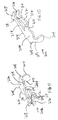
- FIG. 1 is an isometric view of a conventional connector including pin grid substrate 10 , a printed circuit board 16 and ZIF electrical connector 20 .
- the pin grid substrate 10 includes a member 12 from which pins 14 outwardly extend.
- the circuit board 16 includes circuitry connected to plated through holes 18 .
- the connector 20 includes a housing 22 , contact elements 24 , a cover 26 and a lever 28 .
- the housing 22 carries a number of regularly spaced cavities (not shown), positioned below the pins 14 .
- a groove 54 is open at one end 60 to accommodate the lever 28 .
- Two blocks 64 with holes 66 therethrough are located on each side of the housing 22 .
- the holes receive roll pins 68 .
- the blocks 64 , holes and roll pins 68 cooperate with structures on the cover 26 to hold the cover on the housing 22 .
- the cover 26 preferably molded with the same material as the housing 22 , contains vertical openings 70 therethrough in the same number and on the same spacing as cavities in the housing 22 .
- Cam block 74 extends down below the lower surface 76 of the cover 26 and is channeled along its downwardly facing surface as indicated by reference numeral 78 .
- One corner of the cover 26 adjacent end 80 is recessed as indicated by reference numeral 82 to provide room for the lever 28 .
- Blocks 84 extend downwardly from opposing sides 86 and 88 of the cover 26 . Both blocks 84 are outwardly displaced relative to the vertical plane of the sides. Further, the block 84 on side 86 is displaced downwardly, relative to top surface 72 , to provide a space for the arm of lever 28 . Each block contains an aperture 90 in each end face to receive roll pin 68 . One section of the member 92 extends outwardly from that side.
- the lever 28 a one piece member, includes handle 96 and cam section 98 .
- the cam section 98 is perpendicular to the handle 96 .
- a short connecting piece 100 joins the handle 96 and cam section 98 and displaces one relative to the other. After loading the contact elements 24 into the cavities, the lever 28 is placed into the housing 22 .
- the connecting piece 100 and the handle 96 extend out of the groove through open end 60 .
- the cover 26 is placed onto the top surface 32 so that blocks 84 slide in between blocks 64 and block 74 enters into the enlarged portion 58 .
- the cover 26 is slidably attached to the housing 22 by sliding the roll pins 68 into the holes 66 in blocks 64 and the apertures 90 in the blocks 84 .
- the cover 26 is actuated against the top surface 32 of the housing 22 by the pivoting handle 96 of the lever 28 .
- the lever 28 provides the actuation necessary to mate the pins 14 with the contacts 24 .
- the contacts 24 may contact the pins 14 at a single point, or at two points.
- a contact 24 that contacts a pin 14 at a single point is less reliable than a contact 24 that contacts a pin 14 at two points.
- a contact 24 that contacts a pin 14 at two points is a redundant contact system.
- a redundant contact system is more reliable than a single contact system in that if the pin is slightly out of position, while one contact may not abut the pin 14 , another contact may abut the pin 14 . In other words, two points of contact are better than one point of contact.
- the two point contact straddles the pin 14 , thereby offering another advantage over the single point contact. That is, the two point contact ensure proper positioning of the pin 14 because the pin 14 is positioned between two contact portions of the two point contact, as opposed to touching one point of contact, as with the single point contact.
- two point contacts are stamped, or blanked, in conjunction with a carrier strip, from a unitary piece of conductive material.
- the two point contact is typically stamped such that the contact portions are oriented in a straight line. That is, one contact portion is located at one end of the line, while the other contact portion is located at the other end of the line.
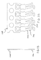
- FIG. 2 is an isometric view of a conventional two point contact 24 .
- FIG. 3 is an illustration of a conventional preformed, blanked two point contact 24 attached to a carrier strip 140 .
- the contact portions 122 are aligned with one another such that the top surfaces 118 of the contact portions 122 are co-linear with each other. That is, line segment AB and line segment CD may be connected by dashed line BC, wherein line AD is a straight line.
- the contact portions 122 are bent as shown in FIG. 2.
- stamping or blanking produces wasted material.
- the stamped, preformed contact typically must be sufficiently wide to allow the proper size of the contacting portions 122 , while at the same time ensuring that the contacting portions 122 will align with, or mirror, each other when the contact is formed.
- a greater portion of conductive material is wasted during the stamping process as compared to the stamping of a single point contact.
- double point contacts typically cannot be stamped the same distance apart, that is, stamped on the same pitch, as that of the cavities in the connector housing.
- Typical connector housing cavities, or receptacles are positioned 1.27 mm, or 0.05′′, apart from one another.
- stamped double point contacts typically cannot be stamped that same distance from each other.
- the pitch, or spacing, between center lines of formed contacts on a carrier strip may be 0.10′′.
- the double point contacts may be skip inserted into the contacts because the contacts may be spaced twice the distance between the cavities of the connector housing.
- a connector housing may include a matrix of 24 cavities by 24 cavities. If the contacts are skip inserted into a row (or column) of the matrix, 12 contacts may be inserted at one time. That is, the double point contacts may be stamped on double the pitch as that of the cavities.
- a pin grid array contact has been developed that comprises a planar main body defining, and arranged within, a primary contact plane.
- the main body has edges along opposed sides and along opposed ends.
- the contact also includes first and second spring beams integral with the main body and extending from a common one of the edges by different first and second lengths, respectively. The first length being longer than the second length.
- the first and second spring beams are aligned with the primary contact plane while the second spring beam may aligned in the primary contact plane.
- the second spring beam may be aligned with the primary contact plane, but may be bent toward the first spring beam, such that the second spring beam is no longer in the primary contact plane.
- the contact further comprises a paddle integral with and extending from one of the edges of the main body.
- the paddle is configured to adhere to a solder ball.
- the main body includes first and second radial positioners configured for positioning the main body into a cavity, or receptacle of a connector housing.
- the first spring beam includes a first contacting portion located at a distal end of the first spring beam remote from the main body.
- the first and second contacting portions lie in different planes; and the first contacting portion is bent into alignment with the second contacting portion.
- the second spring beam includes a second contacting portion located at a distal end of the second spring beam remote from the main body. The first and second spring beams are shifted laterally from one another with respect to a center line of the main body. The lateral shift is in a direction parallel to the primary contact plane.
- the second spring beam While in the flat, stamped state, the second spring beam is offset from the first spring beam by a predetermined angle.
- the stamped double contacts are coplanar with the carrier strip.
- the first and second spring beams are bent such that the first and second spring beams lie in different first and second planes, while the first contacting portion remains laterally aligned with the second contacting portion.
- Certain embodiments of the present invention provide a method of forming a pin grid array contact.
- the method comprises stamping a contact having a main body formed with first and second spring beams from a planar single sheet of conductive material, in which the first and second spring beams have different first and second lengths that extend along first and second longitudinal axes, respectively.
- the first and second spring beams are aligned at an acute angle with one another and initially oriented in a primary contact plane defined by the main body.
- the method also comprises bending the second spring beam with respect to the main body until the second spring beam is located in a second beam plane that is separate from the primary contact plane.
- the method comprises shifting the first and second spring beams laterally from one another with respect to a center line of the main body. The shifting step occurring in a direction parallel to the primary contact plane.
- the method comprises aligning a first contacting portion of the first spring beam into alignment with a second contacting portion of the second spring beam.
- Certain embodiments of the present invention also provide the following steps: providing a carrier strip integral with a plurality of the contacts in the primary contact plan; positioning adjacent contacts so that a distance between center lines of the adjacent contacts corresponds to a distance between two cavities located on a connector housing; and stamping a paddle on the main body and bending the paddle to be perpendicular to the main body of each contact.
- FIG. 1 is an isometric view of a conventional connector with a pin grid substrate, a printed circuit board and a ZIF (zero insertion force) electrical connector.
- FIG. 2 is an isometric view of a conventional two point contact.
- FIG. 3 illustrates a conventional preformed, blanked two point contact attached to a carrier strip.
- FIG. 4 is a front view of a carrier strip carrying a plurality of flat blanked contacts formed in accordance with an embodiment of the present invention.
- FIG. 5 is an end view of a carrier strip carrying a plurality of flat blanked contacts formed in accordance with an embodiment of the present invention.
- FIG. 6 is a front view of a contact formed in accordance with an embodiment of the present invention.
- FIG. 7 is a side view of a contact formed in accordance with an embodiment of the present invention.
- FIG. 8 is a top view of a contact formed in accordance with an embodiment of the present invention.
- FIGS. 9 and 10 are isometric views of a contact formed in accordance with an embodiment of the present invention.
- FIG. 11 is a front view of a carrier strip carrying a plurality of flat blanked contacts formed in accordance with an alternative embodiment of the present invention.
- FIG. 12 is an end view of a carrier strip carrying a plurality of flat blanked contacts formed in accordance with an alternative embodiment of the present invention.
- FIG. 13 is a front view of a contact formed in accordance with an alternative embodiment of the present invention.
- FIG. 14 is a side view of a contact formed in accordance with an alternative embodiment of the present invention.
- FIG. 15 is a top view of a contact formed in accordance with an alternative embodiment of the present invention.
- FIGS. 16 and 17 are isometric views of a contact formed in accordance with an alternative embodiment of the present invention.
- FIG. 18 is a side view of a contact and a carrier strip prior to insertion of the contact into the connector housing according to an embodiment of the present invention.
- FIG. 19 is a side view of a contact positioned within a cavity of a connector housing according to an embodiment of the present invention.
- FIG. 20 is a cross-sectional view of a cavity formed in accordance with an embodiment of the present invention.
- FIG. 21 is a cross-sectional view of a cavity formed in accordance with an embodiment of the present invention.
- FIG. 22 is a front view of a carrier strip carrying a plurality of flat blanked contacts formed in accordance with an embodiment of the present invention.
- FIG. 23 is an end view of a carrier strip carrying a plurality of flat blanked contacts formed in accordance with an embodiment of the present invention.
- FIG. 24 is a side view of a contact formed in accordance with an embodiment of the present invention.
- FIGS. 25 and 26 are isometric views of a contact formed in accordance with an embodiment of the present invention.
- FIG. 27 is a side view of a contact and a carrier strip prior to insertion of the contact into the connector housing according to an embodiment of the present invention.
- FIG. 28 is an isometric view of a contact and carrier strip prior to insertion of the contact into the connector housing according to an embodiment of the present invention.
- FIG. 4 is a front view of a carrier strip 240 carrying a plurality of flat blanked contacts 202 formed in accordance with an embodiment of the present invention.
- FIG. 5 is an end view of a carrier strip 240 carrying a plurality of flat blanked contacts 202 formed in accordance with an embodiment of the present invention.
- the carrier strip 240 and the flat blanked contacts 202 are formed from a unitary, planar piece of conductive material, such as a copper alloy having a suitable plating, such as tin, lead or nickel.
- the carrier strip 240 includes cavities 236 and connection joints 234 that join the carrier strip 240 to the flat blanked contacts 202 .
- the connection joints 234 may be perforated to facilitate the release of the individual contacts 202 from the carrier strip 240 .
- Each flat blanked contact 202 is coplanar with the carrier strip 240 .
- Each contact 202 includes a paddle 204 , first radial positioners 208 , second radial positioners 210 , a main body 206 , a first spring beam 212 , a second spring beam 214 , a first contacting portion 216 connected to the first spring beam 212 , and a second contacting portion 218 connected to the second spring beam 214 .
- the main body 206 has opposed side edges 246 , 247 and opposed end edges 248 , 249 .
- the first and second spring beams 212 and 214 are stamped integral with, and extend outward from end edge 249 .
- the first spring beam 212 extends a length 250 from the end edge 249
- the second spring beam 214 extends a length 251 from the same end edge 249
- the first and second spring beams 212 and 214 are shifted laterally in the direction of arrow 213 from one another on opposite sides of the center line 230 .
- the lateral shift is parallel to the primary contact plane.
- the center line of each contact 202 is denoted by reference line 230 that is contained within a primary contact plane.
- the width of the carrier strip 240 and the contacts 202 in the preformed blanked state, as shown in FIG. 5, is denoted by W S .
- the distance (D C ) represents the distance between the center lines 230 of adjacent contacts 202 .
- the contacts 202 may be flat blanked such that the distance (D C ) between their center lines 230 is less than or equal to 1.27 mm, or 0.05′′ apart from one another.
- the carrier strip 240 and the contacts 202 are stamped, or blanked, from a single planar sheet, coil, or slab of conductive material. As shown in FIG. 4, while in the blanked, preformed state, the first spring beam 212 is longer than the second spring beam 214 . In the preformed state, the first spring beam 212 and the second spring beam 214 are aligned in the primary contact plane, which is defined by the main body 206 . Once stamped, the second spring beam 214 is angled away, or offset, from the first spring beam 212 by approximately 20°. Further, the first contacting portion 216 and the second contacting portion 218 are not aligned with one another while in the blanked, preformed state.
- first and second spring beams 212 and 214 are oriented as shown in FIG. 4 while in the blanked, preformed state, adjacent contacts 202 may be blanked, or stamped, closer to one another than previously blanked contacts. Thus, the contacts 202 may be blanked, or stamped, such that the distance (D C ) between respective center lines 230 is the same distance between connector housing cavities, or receptacles.
- the distance (D C ) between the center lines 230 of adjacent contacts 202 may be 1.27 mm, or 0.05′′, which is also the same distance between the centers of connector housing receptacles, or cavities, into which the contacts are eventually positioned.
- the contacts 202 are stamped or blanked closer together, more of the original sheet of conductive material is utilized, thereby producing less wasted conductive material than in previous blanking processes.
- the forming process which includes a series of bends and cants of the contacts 202 by way of a forming die, as described below with respect to FIGS. 6 - 10 , enables the contacts 202 to be blanked within a close spacing, such as 1.27 mm, or 0.05′′, from one another.
- FIG. 6 is a front view of a contact 202 formed in accordance with an embodiment of the present invention.
- FIG. 7 is a side view of the contact 202 formed in accordance with an embodiment of the present invention.
- FIG. 8 is a top view of the contact 202 formed in accordance with an embodiment of the present invention.
- FIGS. 9 and 10 are isometric views of the contact 202 formed in accordance with an embodiment of the present invention.
- the formed contact 202 is similar to the flat blanked contact 202 except that the formed contact 202 has been bent, canted and otherwise formed through a die.
- the contact 202 may be formed while still on the carrier strip 240 .
- the first spring beam 212 is bent out from the plane of the main body 206 at bend 312 .
- the first spring beam 212 is bent to be parallel with, but no longer coplanar with, the plane of the main body 206 (and therefore the carrier strip 240 ).
- the second spring beam 214 is canted, at bend 314 , toward the first spring beam 212 such that the first contacting portion 216 and the second contacting portion 218 are aligned with each other, that is, the first contacting portion 216 is parallel, but not coplanar, with the second contacting portion 218 .
- the second spring beam 214 While the second spring beam 214 is canted toward the first spring beam 212 , the second spring beam 214 remains in the same plane as the main body 206 (and the carrier strip 240 , when the contact 202 is formed while it is still attached to the carrier strip 240 ). That is, the second spring beam 214 remains aligned in the primary contact plane, while the first spring beam 212 is aligned with, but not in, the primary contact plane.
- the bending and canting of the spring beams 212 and 214 allows the spring beams 212 and 214 to be stamped closer to one another, than in previous stamping, or blanking processes.
- first contacting portion 216 and the second contacting portion 218 are formed such that first and second contacting tips 316 and 318 are bent outward from the plane of the main body 206 , that is, the primary contact plane. Additionally, during the forming process, the paddle 204 is bent at bend 307 such that the plane of the paddle 204 is perpendicular to the plane of the main body 206 .
- adjacent contacts 202 remain the distance D C from one another.
- an entire row, or column, of contacts 202 may be inserted into cavities of a connector housing because the distance (D C ) between the center lines 230 of adjacent contacts 202 remains the same as the distance between the centers of connector housing receptacles, or cavities, into which the contacts 202 are eventually positioned.
- a connector housing may be oriented in a pin grid array that is 25 cavities by 25 cavities. Because the contacts 202 may be formed on the carrier so that they are the same distance apart as the cavities, the contacts 202 may be inserted simultaneously from the carrier strip 240 into a row or column of cavities.
- FIG. 18 is a side view of a contact 202 and a carrier strip 240 prior to insertion of the contact 202 into the connector housing according to an embodiment of the present invention.
- solder balls may be positioned on the paddles 204 .
- a solder ball having a diameter of approximately 0.03′′ may be attached to the bottom of the paddle 204 .
- the paddles 204 may be oriented in a plane that is perpendicular to the carrier strip 240 .
- the contacts 202 may be bent at the connection joints 234 such that the main bodies 206 of the contacts 202 are perpendicular to the carrier strip 240 .
- the solder balls may be attached to the paddles 204 before insertion, or the solder balls may be positioned within the cavities prior to insertion of the contacts 202 into the cavities.
- FIG. 19 is a side view of a contact 202 positioned within a cavity 704 of a connector housing 701 according to an embodiment of the present invention.
- a solder ball 702 is positioned between the paddle 204 and the cavity base 703 .
- each paddle 204 Prior to insertion into the connector housing 701 , each paddle 204 is oriented in a plane that is parallel to the surface of the connector housing 701 .
- the contacts 202 are inserted into cavities 704 to a depth at which the carrier strip 240 abuts against or is closest to the connector housing 701 , the carrier strip 240 is severed from the contacts 202 at the connection joints 234 .
- the carrier strips 240 may be severed shortly after the first and second contacting portions 216 and 218 are started into the cavities 704 (if inserted upward) or shortly after the paddle 204 is started into the cavities 704 (if inserted downward).
- the carrier strip 240 may be severed from the contacts 202 before insertion, in which case a separate insertion strip may engage the contacts 202 by the contacting portions 216 and 218 and position the contacts 202 into the cavities 704 , or receptacles of the connector housing 701 .
- individual positioning of the contacts 202 is not required. For example, if the contacts 202 are bent in the carrier strip 240 , all of the contacts 202 may be mass inserted into the cavities 704 of the connector housing 701 .
- a separate insertion strip may attach to the first and second contacting portions 216 and 218 , such as by an electromagnetic force, while the contacts 202 are severed from the carrier strip. In both cases, the contacts 202 remain the same distance (D C ) from one another. Therefore, the insertion process is more efficient than previous insertion processes.
- the first radial positioners 208 engage the interior walls of the cavities 704 and facilitate proper alignment of the contacts 202 during the assembly stroke, that is, the insertion process.
- the second radial positioners 210 engage the interior walls of the cavities such that there are four points of contact between each contact 202 and the interior walls of the cavity 704 into which the contact 202 is inserted.
- each cavity 704 within the connector housing 701 receives a contact 202 and retains the contact 202 through the first and second radial positioners 208 and 210 .
- each paddle 204 rests on a base 703 of a cavity 704 such that an attached solder ball 702 is positioned between the base 703 of the cavity 704 and the paddle 204 .
- solder balls 702 may be attached directly to the paddles 204 .
- solder balls 702 may be inserted into the cavities 704 before the contacts 202 are inserted into the cavities 704 .
- the contact 202 may include a solder pin, which receives a solder ball 702 .
- the connector housing 701 , the printed circuit board and the pin grid substrate may be compressed together.
- conductive pins such as pins 14 shown in FIG. 1
- the mating surface of each pin 14 is laterally slid between the first and second contacting portions 216 and 218 (such as in the direction of arrow 317 of FIG. 9).
- the tips 316 and 318 (as shown in FIG.
- first and second contacting portions 216 and 218 are bent outward in order to facilitate proper insertion of a pin. That is, the orientation of the tips 316 and 318 decreases the possibility of a pin 14 stubbing, or otherwise not being fully engaged with, the first and second contacting portions 216 and 218 .
- the actuation provided by an actuation mechanism slides the pins 14 between the first and second contacting portions 216 and 218 .
- each pin 14 is contacted on opposite sides by a contact 202 . That is, the first contacting portion 216 and the second contacting portion 218 of a contact 202 simultaneously contact one pin 14 .
- FIG. 20 is a cross-sectional view of a connector housing 801 having a cavity 706 and housing base 710 formed in accordance with an embodiment of the present invention.
- the contact 202 may be inserted from the cavity base 703 when the housing base 710 is removed. After the contact 202 is positioned within the cavity 706 , the housing base 710 is attached to the cavity 706 .
- FIG. 21 is a cross-sectional view of a connector housing 802 having a cavity 712 formed in accordance with an embodiment of the present invention.
- the connector housing 802 includes a base 803 and a channel 804 .
- the channel 804 may be used as a path to deliver a solder ball and/or a conductive path to electrical elements (not shown) and/or traces (not shown) within the connector housing.
- FIGS. 11 - 17 illustrate contacts 402 formed in accordance with an alternative embodiment of the present invention. Common reference numerals have been assigned to common structure of the contacts 402 of FIGS. 11 - 17 and the contact 202 of FIGS. 4 - 10 .
- the contact 402 includes a solder depression 604 , instead of the paddle 204 of the contact 202 as shown in FIGS. 4 - 10 .
- the solder depression 604 contacts a solder ball positioned on the base of the cavity.
- FIG. 22 is a front view of a carrier strip 1240 carrying a plurality of flat blanked contacts 1202 formed in accordance with an embodiment of the present invention.
- FIG. 23 is an end view of a carrier strip 1240 carrying a plurality of flat blanked contacts 1202 formed in accordance with an embodiment of the present invention.
- the first spring beam 1212 may be slightly longer and narrower than the spring beam 212 .
- the second spring beam 1214 may be slightly narrower than the spring beam 214 .
- the angle of the offset between spring beam 1214 and spring beam 1212 may be slightly more than that between spring beam 214 and spring beam 212 .
- the same beam configuration may be used with contacts 402 .
- FIG. 24 is a front view of a contact 1202 formed in accordance with an embodiment of the present invention.
- FIGS. 25 and 26 are isometric views of the contact 1202 formed in accordance with an embodiment of the present invention.
- the second spring beam 1214 may be bent toward the first spring beam 1212 .
- FIGS. 27 and 28 show the contact 1202 and a carrier strip 1240 prior to insertion of the contact 1202 into the connector housing according to an embodiment of the present invention.
- Various embodiments of the present invention provide a more efficient method of blanking, or stamping, micro pin grid array contacts, and provide a more efficient method of inserting the contacts into cavities of a connector housing.
Landscapes
- Coupling Device And Connection With Printed Circuit (AREA)
Abstract
Description
- Certain embodiments of the present invention relate to a pin grid array contact, and more particularly to an pin grid array contact that provides more efficient assembly into an electrical connector.
- Connectors are known for interconnecting various electrical media components, such as printed circuit boards (PCB), discrete circuit components, flex circuits and the like. Many printed circuit boards are connected to pin grid substrates by way of ZIF (zero insertion force) connectors. Typically, ZIF connectors include single or double point contacts that connect conductive pins, which extend from the pin grid substrate, to traces on the printed circuit board. Typically, the pin grid substrate, the connector, and printed circuit board are compressed together in order to ensure a conductive path between the pins, contacts and the traces on the printed circuit board.
- FIG. 1 is an isometric view of a conventional connector including
pin grid substrate 10, a printedcircuit board 16 and ZIFelectrical connector 20. Thepin grid substrate 10 includes amember 12 from whichpins 14 outwardly extend. Thecircuit board 16 includes circuitry connected to plated throughholes 18. Theconnector 20 includes ahousing 22,contact elements 24, acover 26 and alever 28. Thehousing 22 carries a number of regularly spaced cavities (not shown), positioned below thepins 14. Agroove 54 is open at oneend 60 to accommodate thelever 28. - Two
blocks 64 withholes 66 therethrough are located on each side of thehousing 22. The holes receiveroll pins 68. Theblocks 64, holes androll pins 68 cooperate with structures on thecover 26 to hold the cover on thehousing 22. Thecover 26, preferably molded with the same material as thehousing 22, containsvertical openings 70 therethrough in the same number and on the same spacing as cavities in thehousing 22. -
Cam block 74 extends down below the lower surface 76 of thecover 26 and is channeled along its downwardly facing surface as indicated byreference numeral 78. One corner of thecover 26adjacent end 80 is recessed as indicated byreference numeral 82 to provide room for thelever 28. -
Blocks 84 extend downwardly fromopposing sides cover 26. Bothblocks 84 are outwardly displaced relative to the vertical plane of the sides. Further, theblock 84 onside 86 is displaced downwardly, relative totop surface 72, to provide a space for the arm oflever 28. Each block contains anaperture 90 in each end face to receiveroll pin 68. One section of themember 92 extends outwardly from that side. - The
lever 28, a one piece member, includeshandle 96 andcam section 98. Thecam section 98 is perpendicular to thehandle 96. A short connectingpiece 100 joins thehandle 96 andcam section 98 and displaces one relative to the other. After loading thecontact elements 24 into the cavities, thelever 28 is placed into thehousing 22. The connectingpiece 100 and thehandle 96 extend out of the groove throughopen end 60. - The
cover 26 is placed onto thetop surface 32 so thatblocks 84 slide in betweenblocks 64 andblock 74 enters into the enlargedportion 58. Thecover 26 is slidably attached to thehousing 22 by sliding theroll pins 68 into theholes 66 inblocks 64 and theapertures 90 in theblocks 84. Thecover 26 is actuated against thetop surface 32 of thehousing 22 by thepivoting handle 96 of thelever 28. Thus, thelever 28 provides the actuation necessary to mate thepins 14 with thecontacts 24. - The
contacts 24 may contact thepins 14 at a single point, or at two points. Typically, acontact 24 that contacts apin 14 at a single point is less reliable than acontact 24 that contacts apin 14 at two points. Acontact 24 that contacts apin 14 at two points, moreover, is a redundant contact system. A redundant contact system is more reliable than a single contact system in that if the pin is slightly out of position, while one contact may not abut thepin 14, another contact may abut thepin 14. In other words, two points of contact are better than one point of contact. - Typically, the two point contact straddles the
pin 14, thereby offering another advantage over the single point contact. That is, the two point contact ensure proper positioning of thepin 14 because thepin 14 is positioned between two contact portions of the two point contact, as opposed to touching one point of contact, as with the single point contact. - Typically, two point contacts are stamped, or blanked, in conjunction with a carrier strip, from a unitary piece of conductive material. The two point contact is typically stamped such that the contact portions are oriented in a straight line. That is, one contact portion is located at one end of the line, while the other contact portion is located at the other end of the line.
- FIG. 2 is an isometric view of a conventional two
point contact 24. FIG. 3 is an illustration of a conventional preformed, blanked twopoint contact 24 attached to acarrier strip 140. As shown in FIG. 3, while in the preformed, blanked state, thecontact portions 122 are aligned with one another such that thetop surfaces 118 of thecontact portions 122 are co-linear with each other. That is, line segment AB and line segment CD may be connected by dashed line BC, wherein line AD is a straight line. In order to form the contact, thecontact portions 122 are bent as shown in FIG. 2. - Forming two point contacts through stamping or blanking, however, produces wasted material. As shown in FIG. 3, the stamped, preformed contact typically must be sufficiently wide to allow the proper size of the contacting
portions 122, while at the same time ensuring that the contactingportions 122 will align with, or mirror, each other when the contact is formed. As a result, a greater portion of conductive material is wasted during the stamping process as compared to the stamping of a single point contact. - Further, unlike single point contacts, double point contacts typically cannot be stamped the same distance apart, that is, stamped on the same pitch, as that of the cavities in the connector housing. Typical connector housing cavities, or receptacles are positioned 1.27 mm, or 0.05″, apart from one another. However, stamped double point contacts typically cannot be stamped that same distance from each other. The pitch, or spacing, between center lines of formed contacts on a carrier strip may be 0.10″. Thus, when the double point contacts are inserted into the cavities, the contacts are individually inserted into the housing cavities. Alternatively the double point contacts may be skip inserted into the contacts because the contacts may be spaced twice the distance between the cavities of the connector housing. For example, a connector housing may include a matrix of 24 cavities by 24 cavities. If the contacts are skip inserted into a row (or column) of the matrix, 12 contacts may be inserted at one time. That is, the double point contacts may be stamped on double the pitch as that of the cavities.
- Thus a need has existed for a more efficient way of method of stamping, or blanking double point micro pin grid array contacts. Further, a need has existed for a more efficient method of inserting double point pin grid array contacts into cavities or receptacles of a connector housing.
- In accordance with certain embodiments of the present invention, A pin grid array contact has been developed that comprises a planar main body defining, and arranged within, a primary contact plane. The main body has edges along opposed sides and along opposed ends. The contact also includes first and second spring beams integral with the main body and extending from a common one of the edges by different first and second lengths, respectively. The first length being longer than the second length. The first and second spring beams are aligned with the primary contact plane while the second spring beam may aligned in the primary contact plane. Optionally the second spring beam may be aligned with the primary contact plane, but may be bent toward the first spring beam, such that the second spring beam is no longer in the primary contact plane. The contact further comprises a paddle integral with and extending from one of the edges of the main body. The paddle is configured to adhere to a solder ball. The main body includes first and second radial positioners configured for positioning the main body into a cavity, or receptacle of a connector housing.
- The first spring beam includes a first contacting portion located at a distal end of the first spring beam remote from the main body. The first and second contacting portions lie in different planes; and the first contacting portion is bent into alignment with the second contacting portion. Also, the second spring beam includes a second contacting portion located at a distal end of the second spring beam remote from the main body. The first and second spring beams are shifted laterally from one another with respect to a center line of the main body. The lateral shift is in a direction parallel to the primary contact plane.
- While in the flat, stamped state, the second spring beam is offset from the first spring beam by a predetermined angle. The stamped double contacts are coplanar with the carrier strip. Then, the first and second spring beams are bent such that the first and second spring beams lie in different first and second planes, while the first contacting portion remains laterally aligned with the second contacting portion.
- Certain embodiments of the present invention provide a method of forming a pin grid array contact. The method comprises stamping a contact having a main body formed with first and second spring beams from a planar single sheet of conductive material, in which the first and second spring beams have different first and second lengths that extend along first and second longitudinal axes, respectively. The first and second spring beams are aligned at an acute angle with one another and initially oriented in a primary contact plane defined by the main body. The method also comprises bending the second spring beam with respect to the main body until the second spring beam is located in a second beam plane that is separate from the primary contact plane. Additionally, the method comprises shifting the first and second spring beams laterally from one another with respect to a center line of the main body. The shifting step occurring in a direction parallel to the primary contact plane. Also, the method comprises aligning a first contacting portion of the first spring beam into alignment with a second contacting portion of the second spring beam.
- Certain embodiments of the present invention also provide the following steps: providing a carrier strip integral with a plurality of the contacts in the primary contact plan; positioning adjacent contacts so that a distance between center lines of the adjacent contacts corresponds to a distance between two cavities located on a connector housing; and stamping a paddle on the main body and bending the paddle to be perpendicular to the main body of each contact.
- FIG. 1 is an isometric view of a conventional connector with a pin grid substrate, a printed circuit board and a ZIF (zero insertion force) electrical connector.
- FIG. 2 is an isometric view of a conventional two point contact.
- FIG. 3 illustrates a conventional preformed, blanked two point contact attached to a carrier strip.
- FIG. 4 is a front view of a carrier strip carrying a plurality of flat blanked contacts formed in accordance with an embodiment of the present invention.
- FIG. 5 is an end view of a carrier strip carrying a plurality of flat blanked contacts formed in accordance with an embodiment of the present invention.
- FIG. 6 is a front view of a contact formed in accordance with an embodiment of the present invention.
- FIG. 7 is a side view of a contact formed in accordance with an embodiment of the present invention.
- FIG. 8 is a top view of a contact formed in accordance with an embodiment of the present invention.
- FIGS. 9 and 10 are isometric views of a contact formed in accordance with an embodiment of the present invention.
- FIG. 11 is a front view of a carrier strip carrying a plurality of flat blanked contacts formed in accordance with an alternative embodiment of the present invention.
- FIG. 12 is an end view of a carrier strip carrying a plurality of flat blanked contacts formed in accordance with an alternative embodiment of the present invention.
- FIG. 13 is a front view of a contact formed in accordance with an alternative embodiment of the present invention.
- FIG. 14 is a side view of a contact formed in accordance with an alternative embodiment of the present invention.
- FIG. 15 is a top view of a contact formed in accordance with an alternative embodiment of the present invention.
- FIGS. 16 and 17 are isometric views of a contact formed in accordance with an alternative embodiment of the present invention.
- FIG. 18 is a side view of a contact and a carrier strip prior to insertion of the contact into the connector housing according to an embodiment of the present invention.
- FIG. 19 is a side view of a contact positioned within a cavity of a connector housing according to an embodiment of the present invention.
- FIG. 20 is a cross-sectional view of a cavity formed in accordance with an embodiment of the present invention.
- FIG. 21 is a cross-sectional view of a cavity formed in accordance with an embodiment of the present invention.
- FIG. 22 is a front view of a carrier strip carrying a plurality of flat blanked contacts formed in accordance with an embodiment of the present invention.
- FIG. 23 is an end view of a carrier strip carrying a plurality of flat blanked contacts formed in accordance with an embodiment of the present invention.
- FIG. 24 is a side view of a contact formed in accordance with an embodiment of the present invention.
- FIGS. 25 and 26 are isometric views of a contact formed in accordance with an embodiment of the present invention.
- FIG. 27 is a side view of a contact and a carrier strip prior to insertion of the contact into the connector housing according to an embodiment of the present invention.
- FIG. 28 is an isometric view of a contact and carrier strip prior to insertion of the contact into the connector housing according to an embodiment of the present invention.
- The foregoing summary, as well as the following detailed description of certain embodiments of the present invention, will be better understood when read in conjunction with the appended drawings. For the purpose of illustrating the invention, there is shown in the drawings, certain embodiments. It should be understood, however, that the present invention is not limited to the arrangements and instrumentality shown in the attached drawings.
- FIG. 4 is a front view of a
carrier strip 240 carrying a plurality of flat blankedcontacts 202 formed in accordance with an embodiment of the present invention. FIG. 5 is an end view of acarrier strip 240 carrying a plurality of flat blankedcontacts 202 formed in accordance with an embodiment of the present invention. Thecarrier strip 240 and the flat blankedcontacts 202 are formed from a unitary, planar piece of conductive material, such as a copper alloy having a suitable plating, such as tin, lead or nickel. Thecarrier strip 240 includescavities 236 andconnection joints 234 that join thecarrier strip 240 to the flat blankedcontacts 202. The connection joints 234 may be perforated to facilitate the release of theindividual contacts 202 from thecarrier strip 240. - Each flat blanked
contact 202 is coplanar with thecarrier strip 240. Eachcontact 202 includes apaddle 204, firstradial positioners 208, secondradial positioners 210, amain body 206, afirst spring beam 212, asecond spring beam 214, a first contactingportion 216 connected to thefirst spring beam 212, and a second contactingportion 218 connected to thesecond spring beam 214. Themain body 206 has opposed side edges 246, 247 and opposed end edges 248, 249. The first and second spring beams 212 and 214 are stamped integral with, and extend outward fromend edge 249. Thefirst spring beam 212 extends alength 250 from theend edge 249, while thesecond spring beam 214 extends alength 251 from thesame end edge 249. The first and second spring beams 212 and 214 are shifted laterally in the direction ofarrow 213 from one another on opposite sides of thecenter line 230. The lateral shift is parallel to the primary contact plane. The center line of eachcontact 202 is denoted byreference line 230 that is contained within a primary contact plane. The width of thecarrier strip 240 and thecontacts 202 in the preformed blanked state, as shown in FIG. 5, is denoted by WS. The distance (DC) represents the distance between thecenter lines 230 ofadjacent contacts 202. Thecontacts 202 may be flat blanked such that the distance (DC) between theircenter lines 230 is less than or equal to 1.27 mm, or 0.05″ apart from one another. - The
carrier strip 240 and thecontacts 202 are stamped, or blanked, from a single planar sheet, coil, or slab of conductive material. As shown in FIG. 4, while in the blanked, preformed state, thefirst spring beam 212 is longer than thesecond spring beam 214. In the preformed state, thefirst spring beam 212 and thesecond spring beam 214 are aligned in the primary contact plane, which is defined by themain body 206. Once stamped, thesecond spring beam 214 is angled away, or offset, from thefirst spring beam 212 by approximately 20°. Further, the first contactingportion 216 and the second contactingportion 218 are not aligned with one another while in the blanked, preformed state. Also, the lengths of the first contactingportion 216 and the second contactingportion 218 do not lie on a common straight line. Because the first and second spring beams 212 and 214 are oriented as shown in FIG. 4 while in the blanked, preformed state,adjacent contacts 202 may be blanked, or stamped, closer to one another than previously blanked contacts. Thus, thecontacts 202 may be blanked, or stamped, such that the distance (DC) betweenrespective center lines 230 is the same distance between connector housing cavities, or receptacles. For example, the distance (DC) between thecenter lines 230 ofadjacent contacts 202 may be 1.27 mm, or 0.05″, which is also the same distance between the centers of connector housing receptacles, or cavities, into which the contacts are eventually positioned. - Further, because the
contacts 202 are stamped or blanked closer together, more of the original sheet of conductive material is utilized, thereby producing less wasted conductive material than in previous blanking processes. The forming process, which includes a series of bends and cants of thecontacts 202 by way of a forming die, as described below with respect to FIGS. 6-10, enables thecontacts 202 to be blanked within a close spacing, such as 1.27 mm, or 0.05″, from one another. - FIG. 6 is a front view of a
contact 202 formed in accordance with an embodiment of the present invention. FIG. 7 is a side view of thecontact 202 formed in accordance with an embodiment of the present invention. FIG. 8 is a top view of thecontact 202 formed in accordance with an embodiment of the present invention. FIGS. 9 and 10 are isometric views of thecontact 202 formed in accordance with an embodiment of the present invention. The formedcontact 202 is similar to the flat blankedcontact 202 except that the formedcontact 202 has been bent, canted and otherwise formed through a die. Thecontact 202 may be formed while still on thecarrier strip 240. - During the forming process, the
first spring beam 212 is bent out from the plane of themain body 206 atbend 312. Thefirst spring beam 212 is bent to be parallel with, but no longer coplanar with, the plane of the main body 206 (and therefore the carrier strip 240). Further, thesecond spring beam 214 is canted, atbend 314, toward thefirst spring beam 212 such that the first contactingportion 216 and the second contactingportion 218 are aligned with each other, that is, the first contactingportion 216 is parallel, but not coplanar, with the second contactingportion 218. While thesecond spring beam 214 is canted toward thefirst spring beam 212, thesecond spring beam 214 remains in the same plane as the main body 206 (and thecarrier strip 240, when thecontact 202 is formed while it is still attached to the carrier strip 240). That is, thesecond spring beam 214 remains aligned in the primary contact plane, while thefirst spring beam 212 is aligned with, but not in, the primary contact plane. The bending and canting of the spring beams 212 and 214 allows the spring beams 212 and 214 to be stamped closer to one another, than in previous stamping, or blanking processes. - Additionally, the first contacting
portion 216 and the second contactingportion 218 are formed such that first and second contactingtips main body 206, that is, the primary contact plane. Additionally, during the forming process, thepaddle 204 is bent atbend 307 such that the plane of thepaddle 204 is perpendicular to the plane of themain body 206. - If the
contacts 202 are formed while still connected to thecarrier strip 240,adjacent contacts 202 remain the distance DC from one another. Thus, an entire row, or column, ofcontacts 202 may be inserted into cavities of a connector housing because the distance (DC) between thecenter lines 230 ofadjacent contacts 202 remains the same as the distance between the centers of connector housing receptacles, or cavities, into which thecontacts 202 are eventually positioned. For example a connector housing may be oriented in a pin grid array that is 25 cavities by 25 cavities. Because thecontacts 202 may be formed on the carrier so that they are the same distance apart as the cavities, thecontacts 202 may be inserted simultaneously from thecarrier strip 240 into a row or column of cavities. - FIG. 18 is a side view of a
contact 202 and acarrier strip 240 prior to insertion of thecontact 202 into the connector housing according to an embodiment of the present invention. In order to fasten thecontacts 202 within the cavities of the connector housing (such ashousing 22, shown in FIG. 1) upon mass insertion of the formedcontacts 202 into the cavities, solder balls may be positioned on thepaddles 204. For example, a solder ball having a diameter of approximately 0.03″ may be attached to the bottom of thepaddle 204. After forming, thepaddles 204 may be oriented in a plane that is perpendicular to thecarrier strip 240. That is, thecontacts 202 may be bent at the connection joints 234 such that themain bodies 206 of thecontacts 202 are perpendicular to thecarrier strip 240. The solder balls may be attached to thepaddles 204 before insertion, or the solder balls may be positioned within the cavities prior to insertion of thecontacts 202 into the cavities. - FIG. 19 is a side view of a
contact 202 positioned within acavity 704 of aconnector housing 701 according to an embodiment of the present invention. Asolder ball 702 is positioned between thepaddle 204 and thecavity base 703. Prior to insertion into theconnector housing 701, eachpaddle 204 is oriented in a plane that is parallel to the surface of theconnector housing 701. Once thecontacts 202 are inserted intocavities 704 to a depth at which thecarrier strip 240 abuts against or is closest to theconnector housing 701, thecarrier strip 240 is severed from thecontacts 202 at the connection joints 234. Optionally, the carrier strips 240 may be severed shortly after the first and second contactingportions paddle 204 is started into the cavities 704 (if inserted downward). Alternatively, thecarrier strip 240 may be severed from thecontacts 202 before insertion, in which case a separate insertion strip may engage thecontacts 202 by the contactingportions contacts 202 into thecavities 704, or receptacles of theconnector housing 701. In each case, individual positioning of thecontacts 202 is not required. For example, if thecontacts 202 are bent in thecarrier strip 240, all of thecontacts 202 may be mass inserted into thecavities 704 of theconnector housing 701. Alternatively, if thecontacts 202 are first severed from thecarrier strip 240, a separate insertion strip may attach to the first and second contactingportions contacts 202 are severed from the carrier strip. In both cases, thecontacts 202 remain the same distance (DC) from one another. Therefore, the insertion process is more efficient than previous insertion processes. - As the
contacts 202 are inserted into thecavities 704 of theconnector housing 701, the firstradial positioners 208 engage the interior walls of thecavities 704 and facilitate proper alignment of thecontacts 202 during the assembly stroke, that is, the insertion process. As thecontacts 202 are further inserted into thecavities 704, the secondradial positioners 210 engage the interior walls of the cavities such that there are four points of contact between eachcontact 202 and the interior walls of thecavity 704 into which thecontact 202 is inserted. Thus, eachcavity 704 within theconnector housing 701 receives acontact 202 and retains thecontact 202 through the first and secondradial positioners paddle 204 rests on abase 703 of acavity 704 such that an attachedsolder ball 702 is positioned between the base 703 of thecavity 704 and thepaddle 204. As mentioned above,solder balls 702 may be attached directly to thepaddles 204. Alternatively,solder balls 702 may be inserted into thecavities 704 before thecontacts 202 are inserted into thecavities 704. Also alternatively, instead of utilizing apaddle 204, thecontact 202 may include a solder pin, which receives asolder ball 702. Once thecontacts 202 are positioned within thecavities 704, the base of theconnector housing 701 is heated in order to solder thepaddles 204 to the bases of the cavities. - After the
contacts 202 are inserted, theconnector housing 701, the printed circuit board and the pin grid substrate may be compressed together. Upon compression, or actuation of the cover against the connector housing 701 (similar to theconnector housing 22 shown in FIG. 1), conductive pins, such aspins 14 shown in FIG. 1, are received by the first and second contactingportions contacts 202. During the mating of thepins 14 to thecontacts 202, the mating surface of eachpin 14 is laterally slid between the first and second contactingportions 216 and 218 (such as in the direction ofarrow 317 of FIG. 9). Thetips 316 and 318 (as shown in FIG. 9) of the first and second contactingportions tips pin 14 stubbing, or otherwise not being fully engaged with, the first and second contactingportions lever 28 in FIG. 1, slides thepins 14 between the first and second contactingportions pins 14 are fully engaged through the actuation provided by the lever, eachpin 14 is contacted on opposite sides by acontact 202. That is, the first contactingportion 216 and the second contactingportion 218 of acontact 202 simultaneously contact onepin 14. - FIG. 20 is a cross-sectional view of a
connector housing 801 having acavity 706 andhousing base 710 formed in accordance with an embodiment of the present invention. In this example, thecontact 202 may be inserted from thecavity base 703 when thehousing base 710 is removed. After thecontact 202 is positioned within thecavity 706, thehousing base 710 is attached to thecavity 706. - FIG. 21 is a cross-sectional view of a
connector housing 802 having acavity 712 formed in accordance with an embodiment of the present invention. Theconnector housing 802 includes abase 803 and achannel 804. Thechannel 804 may be used as a path to deliver a solder ball and/or a conductive path to electrical elements (not shown) and/or traces (not shown) within the connector housing. - FIGS. 11-17 illustrate
contacts 402 formed in accordance with an alternative embodiment of the present invention. Common reference numerals have been assigned to common structure of thecontacts 402 of FIGS. 11-17 and thecontact 202 of FIGS. 4-10. Thecontact 402, however, includes asolder depression 604, instead of thepaddle 204 of thecontact 202 as shown in FIGS. 4-10. Thus, when thecontact 402 is inserted into a cavity of the connector housing, thesolder depression 604 contacts a solder ball positioned on the base of the cavity. - FIG. 22 is a front view of a
carrier strip 1240 carrying a plurality of flat blankedcontacts 1202 formed in accordance with an embodiment of the present invention. FIG. 23 is an end view of acarrier strip 1240 carrying a plurality of flat blankedcontacts 1202 formed in accordance with an embodiment of the present invention. A comparison between FIGS. 22 and 23 with FIGS. 4 and 5 show that thefirst spring beam 1212 may be slightly longer and narrower than thespring beam 212. Also, thesecond spring beam 1214 may be slightly narrower than thespring beam 214. Also, the angle of the offset betweenspring beam 1214 andspring beam 1212 may be slightly more than that betweenspring beam 214 andspring beam 212. The same beam configuration may be used withcontacts 402. - FIG. 24 is a front view of a
contact 1202 formed in accordance with an embodiment of the present invention. FIGS. 25 and 26 are isometric views of thecontact 1202 formed in accordance with an embodiment of the present invention. As shown in FIGS. 24-26, thesecond spring beam 1214 may be bent toward thefirst spring beam 1212. FIGS. 27 and 28 show thecontact 1202 and acarrier strip 1240 prior to insertion of thecontact 1202 into the connector housing according to an embodiment of the present invention. - Various embodiments of the present invention provide a more efficient method of blanking, or stamping, micro pin grid array contacts, and provide a more efficient method of inserting the contacts into cavities of a connector housing.
- While the invention has been described with reference to certain embodiments, it will be understood by those skilled in the art that various changes may be made and equivalents may be substituted without departing from the scope of the invention. In addition, many modifications may be made to adapt a particular situation or material to the teachings of the invention without departing from its scope. Therefore, it is intended that the invention not be limited to the particular embodiment disclosed, but that the invention will include all embodiments falling within the scope of the appended claims.
Claims (27)
Priority Applications (3)
| Application Number | Priority Date | Filing Date | Title |
|---|---|---|---|
| US10/119,072 US6669499B2 (en) | 2002-04-09 | 2002-04-09 | Contact for pin grid array connector and method of forming same |
| TW092108017A TWI274445B (en) | 2002-04-09 | 2003-04-08 | Contact for pin grid array connector and method of forming same |
| CNB031407633A CN100334781C (en) | 2002-04-09 | 2003-04-09 | Contact part for plug grid array connector and forming method thereof |
Applications Claiming Priority (1)
| Application Number | Priority Date | Filing Date | Title |
|---|---|---|---|
| US10/119,072 US6669499B2 (en) | 2002-04-09 | 2002-04-09 | Contact for pin grid array connector and method of forming same |
Publications (2)
| Publication Number | Publication Date |
|---|---|
| US20030190833A1 true US20030190833A1 (en) | 2003-10-09 |
| US6669499B2 US6669499B2 (en) | 2003-12-30 |
Family
ID=28674532
Family Applications (1)
| Application Number | Title | Priority Date | Filing Date |
|---|---|---|---|
| US10/119,072 Expired - Fee Related US6669499B2 (en) | 2002-04-09 | 2002-04-09 | Contact for pin grid array connector and method of forming same |
Country Status (3)
| Country | Link |
|---|---|
| US (1) | US6669499B2 (en) |
| CN (1) | CN100334781C (en) |
| TW (1) | TWI274445B (en) |
Families Citing this family (5)
| Publication number | Priority date | Publication date | Assignee | Title |
|---|---|---|---|---|
| CN2598183Y (en) * | 2003-01-29 | 2004-01-07 | 莫列斯公司 | Conducting terminal and electric connector using same |
| US7182634B2 (en) * | 2004-06-29 | 2007-02-27 | Intel Corporation | Connector cell having a supported conductive extension |
| US7318736B1 (en) * | 2006-08-08 | 2008-01-15 | Sensata Technologies, Inc. | Burn-in sockets for BGA IC devices having an integrated slider with full ball grid compatibility |
| TWM344660U (en) * | 2008-03-31 | 2008-11-11 | Hon Hai Prec Ind Co Ltd | Electrical contact |
| TWI577094B (en) * | 2014-08-28 | 2017-04-01 | 連展科技股份有限公司 | Electrical plug connector |
Family Cites Families (12)
| Publication number | Priority date | Publication date | Assignee | Title |
|---|---|---|---|---|
| US4498725A (en) | 1982-06-02 | 1985-02-12 | Amp Incorporated | Electrical connector |
| DE3669811D1 (en) * | 1985-12-13 | 1990-04-26 | Siemens Ag | CONTACT SPRING. |
| JPH0751736Y2 (en) * | 1987-05-08 | 1995-11-22 | ミネソタ マイニング アンド マニュファクチュアリング カンパニー | Thin female connector for electrical connection |
| US5456613A (en) * | 1993-07-16 | 1995-10-10 | Tongrand Limited | Zero insertion force connector and contact therein |
| US5443591A (en) * | 1994-05-24 | 1995-08-22 | Tsai; Tien C. | Connector socket |
| US6024584A (en) | 1996-10-10 | 2000-02-15 | Berg Technology, Inc. | High density connector |
| TW392975U (en) | 1998-09-29 | 2000-06-01 | Hon Hai Prec Ind Co Ltd | Electrical connector |
| TW443622U (en) | 1999-03-02 | 2001-06-23 | Hon Hai Prec Ind Co Ltd | Electrical connector |
| TW438109U (en) | 1999-03-19 | 2001-05-28 | Hon Hai Prec Ind Co Ltd | Terminal of electrical connector |
| US6264490B1 (en) * | 1999-11-22 | 2001-07-24 | Berg Technology, Inc. | Electrical connector having female contact |
| US6312276B1 (en) * | 2001-01-17 | 2001-11-06 | Fullcom Technology Corp. | Terminals for achieving preferred electric and mechanic connection |
| US6450826B1 (en) * | 2001-11-26 | 2002-09-17 | Hon Hai Precision Ind. Co., Ltd. | Contact of electrical connector |
-
2002
- 2002-04-09 US US10/119,072 patent/US6669499B2/en not_active Expired - Fee Related
-
2003
- 2003-04-08 TW TW092108017A patent/TWI274445B/en not_active IP Right Cessation
- 2003-04-09 CN CNB031407633A patent/CN100334781C/en not_active Expired - Fee Related
Also Published As
| Publication number | Publication date |
|---|---|
| TWI274445B (en) | 2007-02-21 |
| CN1459888A (en) | 2003-12-03 |
| CN100334781C (en) | 2007-08-29 |
| TW200403900A (en) | 2004-03-01 |
| US6669499B2 (en) | 2003-12-30 |
Similar Documents
| Publication | Publication Date | Title |
|---|---|---|
| US6592382B2 (en) | Simplified board connector | |
| CN101171724B (en) | Two-piece surface mount head assembly with planar alignment surface | |
| US5637008A (en) | Zero insertion force miniature grid array socket | |
| US6488513B1 (en) | Interposer assembly for soldered electrical connections | |
| US5221210A (en) | Circuite board connector | |
| US6719573B2 (en) | Electrical connector assembly and method of assembling same | |
| JPH0311102B2 (en) | ||
| US7086913B2 (en) | Surface mount header assembly having a planar alignment surface | |
| US6079988A (en) | Electrical connector having spring contact with double contact projections as a contact region with contact pad of an external electronic component | |
| KR100344050B1 (en) | Low profile electrical connector for a pga package and terminals therefore | |
| KR100243753B1 (en) | Electrical connector assembly and ejector for connecting the IC card to the printed circuit board | |
| WO2001061792A1 (en) | Printed circuit connector | |
| KR100739916B1 (en) | Connector in which a stress applied upon connection is received by a contact | |
| EP1548888B1 (en) | PGA Type IC Socket | |
| US6669499B2 (en) | Contact for pin grid array connector and method of forming same | |
| US6979219B2 (en) | Zero insertion force dual beam surface mount contact | |
| US6749442B2 (en) | Flexible circuit board connecting device | |
| EP0361971A2 (en) | Electrical connector | |
| KR101029668B1 (en) | Surface Mount Header Assemblies | |
| US6413110B2 (en) | Zero insertion force socket | |
| JPH1012342A (en) | Contact and ic socket provided with the contact | |
| EP1091628A2 (en) | Electrical interconnection socket apparatus | |
| US6974331B2 (en) | Socket connector carrying flexible contacts | |
| US5641297A (en) | Zero insertion force miniature grid array socket | |
| JP2001143795A (en) | Connector for fpc/ffc without soldering |
Legal Events
| Date | Code | Title | Description |
|---|---|---|---|
| AS | Assignment |
Owner name: TYCO ELECTRONICS CORPORATION, PENNSYLVANIA Free format text: ASSIGNMENT OF ASSIGNORS INTEREST;ASSIGNORS:WHYNE, RICHARD NICHOLAS;GRZYBOWSKI, RICHARD W.;REEL/FRAME:013053/0789 Effective date: 20020404 |
|
| FPAY | Fee payment |
Year of fee payment: 4 |
|
| FPAY | Fee payment |
Year of fee payment: 8 |
|
| REMI | Maintenance fee reminder mailed | ||
| LAPS | Lapse for failure to pay maintenance fees | ||
| STCH | Information on status: patent discontinuation |
Free format text: PATENT EXPIRED DUE TO NONPAYMENT OF MAINTENANCE FEES UNDER 37 CFR 1.362 |
|
| STCH | Information on status: patent discontinuation |
Free format text: PATENT EXPIRED DUE TO NONPAYMENT OF MAINTENANCE FEES UNDER 37 CFR 1.362 |
|
| FP | Lapsed due to failure to pay maintenance fee |
Effective date: 20151230 |