US20030190784A1 - Method of forming floating gate of flash memory - Google Patents
Method of forming floating gate of flash memory Download PDFInfo
- Publication number
- US20030190784A1 US20030190784A1 US10/064,077 US6407702A US2003190784A1 US 20030190784 A1 US20030190784 A1 US 20030190784A1 US 6407702 A US6407702 A US 6407702A US 2003190784 A1 US2003190784 A1 US 2003190784A1
- Authority
- US
- United States
- Prior art keywords
- dielectric layer
- floating gate
- layer
- forming
- opening
- Prior art date
- Legal status (The legal status is an assumption and is not a legal conclusion. Google has not performed a legal analysis and makes no representation as to the accuracy of the status listed.)
- Granted
Links
- 238000000034 method Methods 0.000 title claims abstract description 42
- 239000000758 substrate Substances 0.000 claims abstract description 18
- 238000002955 isolation Methods 0.000 claims description 26
- 239000000463 material Substances 0.000 claims description 15
- 238000005530 etching Methods 0.000 claims description 12
- 238000005498 polishing Methods 0.000 claims description 10
- BOTDANWDWHJENH-UHFFFAOYSA-N Tetraethyl orthosilicate Chemical compound CCO[Si](OCC)(OCC)OCC BOTDANWDWHJENH-UHFFFAOYSA-N 0.000 claims description 6
- 229910021420 polycrystalline silicon Inorganic materials 0.000 claims description 6
- 229920005591 polysilicon Polymers 0.000 claims description 6
- 238000004518 low pressure chemical vapour deposition Methods 0.000 claims description 4
- 229910052814 silicon oxide Inorganic materials 0.000 claims description 4
- 238000001039 wet etching Methods 0.000 claims description 4
- 229910052581 Si3N4 Inorganic materials 0.000 claims description 3
- VYPSYNLAJGMNEJ-UHFFFAOYSA-N Silicium dioxide Chemical compound O=[Si]=O VYPSYNLAJGMNEJ-UHFFFAOYSA-N 0.000 claims description 3
- HQVNEWCFYHHQES-UHFFFAOYSA-N silicon nitride Chemical compound N12[Si]34N5[Si]62N3[Si]51N64 HQVNEWCFYHHQES-UHFFFAOYSA-N 0.000 claims description 3
- 238000000059 patterning Methods 0.000 claims 2
- 238000000151 deposition Methods 0.000 description 5
- 230000008901 benefit Effects 0.000 description 4
- 239000003989 dielectric material Substances 0.000 description 4
- 229920002120 photoresistant polymer Polymers 0.000 description 4
- 230000000717 retained effect Effects 0.000 description 4
- 238000004519 manufacturing process Methods 0.000 description 2
- 238000012986 modification Methods 0.000 description 2
- 230000004048 modification Effects 0.000 description 2
- 238000007796 conventional method Methods 0.000 description 1
- 230000008021 deposition Effects 0.000 description 1
- 238000005137 deposition process Methods 0.000 description 1
- 230000000694 effects Effects 0.000 description 1
- 230000010354 integration Effects 0.000 description 1
- 230000003647 oxidation Effects 0.000 description 1
- 238000007254 oxidation reaction Methods 0.000 description 1
- 239000004065 semiconductor Substances 0.000 description 1
Images


Classifications
-
- H—ELECTRICITY
- H10—SEMICONDUCTOR DEVICES; ELECTRIC SOLID-STATE DEVICES NOT OTHERWISE PROVIDED FOR
- H10B—ELECTRONIC MEMORY DEVICES
- H10B41/00—Electrically erasable-and-programmable ROM [EEPROM] devices comprising floating gates
- H10B41/30—Electrically erasable-and-programmable ROM [EEPROM] devices comprising floating gates characterised by the memory core region
-
- H—ELECTRICITY
- H10—SEMICONDUCTOR DEVICES; ELECTRIC SOLID-STATE DEVICES NOT OTHERWISE PROVIDED FOR
- H10B—ELECTRONIC MEMORY DEVICES
- H10B69/00—Erasable-and-programmable ROM [EPROM] devices not provided for in groups H10B41/00 - H10B63/00, e.g. ultraviolet erasable-and-programmable ROM [UVEPROM] devices
Definitions
- the present invention relates to a method of manufacturing a semiconductor device. More particularly, the present invention relates to a method of forming the floating gate of a flash memory unit.
- Flash memory is a type of electrical erasable programmable read only memory (EEPROM). Data can be written into or erased from the EEPROM. Most important, however, is that the data is retained even after power supply is cut. Due to versatility of the EEPROM, most personal computer and electronic equipment employ this type of memory. Flash memory is also a type of non-volatile memory (NVM) having the advantages of occupying a small volume, having a fast accessing speed and consuming very little power. Since data inside the flash memory is erased in a block-by block manner, operating speed is exceptionally fast.
- NVM non-volatile memory
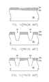
- FIGS. 1A through 1F are cross-sectional views showing the progression of steps for forming the floating gate of a conventional flash memory.
- a substrate 100 having a tunnel oxide layer 102 and a first floating gate layer 104 thereon is provided as shown in FIG. 1A.
- the first floating gate layer 104 , the tunnel oxide layer 102 and the substrate 100 are patterned to form an opening 106 in the substrate 100 , a patterned floating gate layer 104 a and a patterned tunnel oxide layer 102 a.
- an oxide layer (not shown) is formed over the first floating gate layer 104 a , filling the opening 106 completely.
- a chemical-mechanical polishing operation is conducted to remove a portion of the oxide layer and expose the first floating gate layer 104 a .
- a shallow trench isolation region 108 is formed.
- a second floating gate layer 110 is formed over the first floating gate layer 104 a and the shallow trench isolation region 108 . Thereafter, a patterned photoresist layer 112 is formed over the second floating gate layer 110 . The photoresist layer 112 exposes the second floating gate layer 110 above the shallow trench isolation region 108 .
- a portion of the second floating gate layer 110 is removed to form a patterned second floating gate layer 110 a .
- the patterned first floating gate layer 104 a and the patterned second floating gate layer 110 a together constitute a floating gate 114 of a flash memory unit.
- the floating gate of each flash memory unit is isolated from the others through the shallow trench isolation regions 108 .
- one object of the present invention is to provide a method of forming the floating gate of a flash memory unit capable of averting the problem caused by a deviation of floating gate alignment.
- a second object of this invention is to provide a method of forming the floating gate of a flash memory unit capable of minimizing the effects due to a reduction of device line width and the limitations of photolithographic process resulting from a reduction in device dimensions.
- a third object of this invention is to provide a method of forming the floating gate of a flash memory unit capable of aligning the floating gates and the shallow trench isolation regions together automatically.
- the invention provides a method of forming the floating gate of a flash memory unit.
- a tunnel oxide layer and a first floating gate layer are sequentially formed over a substrate.
- the first floating gate layer, the tunnel oxide layer and the substrate are patterned to form an opening.
- a first dielectric layer is formed over the substrate partially filling the opening.
- a second dielectric layer is formed over the first dielectric layer totally filling the opening.
- a high etching selectivity ratio exists between the second dielectric layer and the first dielectric layer.
- a chemical-mechanical polishing operation is conducted to planarize the second dielectric layer and expose the first dielectric layer.
- a wet etching operation is conducted to remove a portion of the first dielectric layer and expose the first floating gate layer, thereby forming a shallow trench isolation region.
- the first dielectric material layer surrounds the shallow trench isolation regions.
- the second dielectric material layer occupies the central portion of the shallow trench isolation regions. Since the second dielectric layer has an etching rate lower than the first dielectric layer, a portion of the second dielectric layer remains after a portion of the first dielectric layer is removed. The retained second dielectric layer rises above the first floating gate layer.
- a second floating gate layer is formed covering the first dielectric layer, the second dielectric layer and the first floating gate layer.
- Another chemical-mechanical polishing operation is conducted to planarize the second floating gate layer and expose the second dielectric layer.
- the first floating gate layer and the second floating gate layer together constitute the floating gate of a flash memory unit. The floating gate of each memory unit is isolated from the others through the shallow trench isolation regions.
- the method of forming the floating gate of a flash memory unit according to this invention is capable of preventing alignment deviation resulting from using a conventional photolithographic process to form the floating gate. Moreover, the method of this invention removes one photolithographic processing step and the floating gate is self-aligned. Furthermore, the method is largely unaffected by a narrowing of line width and aligning limitations associated with a photolithographic process.
- FIGS. 1A through 1F are cross-sectional views showing the progression of steps for forming the floating gate of a conventional flash memory.
- FIGS. 2A through 2H are cross-sectional views showing the progression of steps for forming the floating gate of a flash memory unit according to one preferred embodiment of this invention.
- FIGS. 2A through 2H are cross-sectional views showing the progression of steps for forming the floating gate of a flash memory unit according to one preferred embodiment of this invention.
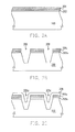
- a substrate 200 having a tunnel oxide layer 202 and a first floating gate layer 204 thereon is provided as shown in FIG. 2A.
- the tunnel oxide layer 202 is formed, for example, by thermal oxidation.
- the first floating gate layer 204 for example, can be a polysilicon layer having a thickness between about 200 ⁇ to 1500 ⁇ .
- the first floating gate layer 204 and the tunnel oxide layer 202 are patterned to form an opening 206 in the substrate 200 , a patterned first floating layer 204 a and a patterned tunnel oxide layer 202 a .
- the first floating gate layer 204 , the tunnel oxide layer 202 and the substrate 200 are patterned, for example, by conducting photolithographic and etching processes.
- a first dielectric layer 208 is formed over the first floating gate layer 204 a but only partially filling the opening 206 .
- the first dielectric layer 208 is formed, for example, by conducting a low-pressure chemical vapor deposition (LPCVD).
- LPCVD low-pressure chemical vapor deposition
- the first dielectric layer 208 having a thickness between about 100 ⁇ to 7000 ⁇ is made from a material, for example, silicon oxide or tetra-ethyl-orthosilicate (TEOS)-silicon oxide. Since the opening 206 is not completely filled by the first dielectric layer 208 , a smaller opening 206 a still exists in the first dielectric layer 208 .
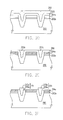
- a second dielectric layer 210 is formed over the first dielectric layer 208 .
- the second dielectric layer 210 completely fills the opening 206 a .
- Material constituting the second dielectric layer 210 must be selected such that the etching selectively ratio between the first dielectric layer 208 and the second dielectric layer 210 must be large. In other words, the second dielectric layer 210 must have an etching rate smaller than the first dielectric layer 208 .
- the second dielectric layer 210 is a silicon nitride layer and has a thickness between about 100 ⁇ to 7000 ⁇ , for example.
- the second dielectric layer 210 is planarized to expose the first dielectric layer 208 .
- the second dielectric layer 210 is planarized, for example, by conducting a chemical-mechanical polishing (CMP).
- CMP chemical-mechanical polishing
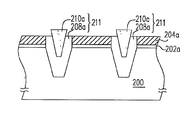
- a portion of the first dielectric layer 208 is removed to expose the first floating gate layer 204 a and form a shallow trench isolation region 211 .
- the first dielectric layer 208 a surrounds the shallow trench isolation region 211 while the second dielectric layer 210 a occupies the central portion of the shallow trench isolation region 211 .
- the first dielectric layer 208 is removed, for example, by wet etching. Since the second dielectric layer 210 has an etching rate lower than the etching rate of the first dielectric layer 208 , the second dielectric layer 210 a is retained after a portion of the first dielectric layer 208 is removed. The retained second dielectric layer 210 a rises higher than the first floating gate layer 204 a . In general, the second dielectric layer 210 a is higher than the first floating gate layer 204 a by between 100 ⁇ to 3000 ⁇ .
- the shallow trench isolation region 211 is formed by first depositing material over the opening 206 to form the first dielectric layer 208 and then depositing material over the first dielectric layer 208 to form the second dielectric layer 210 and fill up the opening 206 . Due to the special characteristic of material deposition, the second dielectric layer 210 a is aligned accurately within the central core of the shallow trench isolation region 211 .
- a second floating gate layer 212 is formed over the first floating gate layer 204 a and the shallow trench isolation layer 212 .
- the second floating gate layer 212 having a thickness of between about 700 ⁇ to 3000 ⁇ is a polysilicon layer, for example.
- the second dielectric layer 212 is planarized to expose the second dielectric layer 210 a in the central portion of the shallow trench isolation region 211 .
- the second floating gate layer 212 is planarized, for example, by conducting a chemical-mechanical polishing (CMP).
- CMP chemical-mechanical polishing
- the first floating gate layer 204 a and the second floating gate layer 212 a together constitute the floating gate 214 of a flash memory unit.
- the floating gate 214 in each memory unit is isolated from the others through the shallow trench isolation regions 211 .
- the floating gates 214 of each flash memory unit are isolated from each other through the shallow trench isolation regions 211 .
- the shallow trench isolation region 211 is formed by depositing dielectric material over the opening 206 to form a conformal layer, that is the first dielectric layer 208 , and then depositing dielectric material over the first dielectric layer 208 to fill the opening 206 . Due to the characteristics of a deposition process, the second dielectric layer 210 a is accurately formed at the central portion of the shallow trench isolation region 211 . In addition, utilizing the shallow trench isolation regions 211 and chemical-mechanical polishing operations, the second floating gate layer 212 a is formed between the shallow trench isolation regions 211 and automatically aligned with the first floating gate layer 204 a.
- the method reduces the number of photolithographic process by one. Moreover, the floating gate is automatically aligned.
Landscapes
- Semiconductor Memories (AREA)
- Non-Volatile Memory (AREA)
- Element Separation (AREA)
Abstract
A method of forming the floating gate of a flash memory unit. A tunnel oxide layer and a first floating gate layer are sequentially formed over a substrate. The first floating gate layer, the tunnel oxide layer and the substrate are patterned to form an opening. A first dielectric layer is formed over the substrate and the interior of the opening but without completely filling the opening. A second dielectric layer is formed over the first dielectric layer so that the opening is completely filled. The second dielectric layer is planarized to expose the first dielectric layer. The first dielectric layer is removed to expose the first floating gate layer. A second floating gate layer is formed over the first floating gate layer. The second floating gate is planarized to expose the second dielectric layer.
Description
- This application claims the priority benefit of Taiwan application serial no.91106950, filed on Apr. 8, 2002.
- 1. Field of Invention
- The present invention relates to a method of manufacturing a semiconductor device. More particularly, the present invention relates to a method of forming the floating gate of a flash memory unit.
- 2. Description of Related Art
- Flash memory is a type of electrical erasable programmable read only memory (EEPROM). Data can be written into or erased from the EEPROM. Most important, however, is that the data is retained even after power supply is cut. Due to versatility of the EEPROM, most personal computer and electronic equipment employ this type of memory. Flash memory is also a type of non-volatile memory (NVM) having the advantages of occupying a small volume, having a fast accessing speed and consuming very little power. Since data inside the flash memory is erased in a block-by block manner, operating speed is exceptionally fast.
- FIGS. 1A through 1F are cross-sectional views showing the progression of steps for forming the floating gate of a conventional flash memory. A
substrate 100 having atunnel oxide layer 102 and a firstfloating gate layer 104 thereon is provided as shown in FIG. 1A. - As shown in FIG. 1B, the first
floating gate layer 104, thetunnel oxide layer 102 and thesubstrate 100 are patterned to form anopening 106 in thesubstrate 100, a patternedfloating gate layer 104 a and a patternedtunnel oxide layer 102 a. - As shown in FIG. 1C, an oxide layer (not shown) is formed over the first
floating gate layer 104 a, filling theopening 106 completely. A chemical-mechanical polishing operation is conducted to remove a portion of the oxide layer and expose the first floatinggate layer 104 a. Hence, a shallowtrench isolation region 108 is formed. - As shown in FIGS. 1D and 1E, a second floating
gate layer 110 is formed over the firstfloating gate layer 104 a and the shallowtrench isolation region 108. Thereafter, a patternedphotoresist layer 112 is formed over the second floatinggate layer 110. Thephotoresist layer 112 exposes the secondfloating gate layer 110 above the shallowtrench isolation region 108. - As shown in FIG. 1F, using the
photoresist layer 112 as an etching mask, a portion of the second floatinggate layer 110 is removed to form a patterned secondfloating gate layer 110 a. The patterned first floatinggate layer 104 a and the patterned second floatinggate layer 110 a together constitute afloating gate 114 of a flash memory unit. The floating gate of each flash memory unit is isolated from the others through the shallowtrench isolation regions 108. - As the level of integration for integrated circuits continues to rise, dimensions of each device shrink. Hence, narrower areas have to be set aside for forming the shallow trench isolation regions. Because the conventional method of forming the floating gate of a flash memory relies on simple photolithographic processes, line width and alignment is severely restricted. In other words, if the opening pattern in the
photoresist layer 112 is not accurately aligned with the shallowtrench isolation regions 108, the secondfloating gate layer 110 a and the firstfloating gate layer 104 a may not align with each other. When this is the case, the shallowtrench isolation regions 108 may not fully isolate thefloating gate 114 of each memory cell from each other. - Accordingly, one object of the present invention is to provide a method of forming the floating gate of a flash memory unit capable of averting the problem caused by a deviation of floating gate alignment.
- A second object of this invention is to provide a method of forming the floating gate of a flash memory unit capable of minimizing the effects due to a reduction of device line width and the limitations of photolithographic process resulting from a reduction in device dimensions.
- A third object of this invention is to provide a method of forming the floating gate of a flash memory unit capable of aligning the floating gates and the shallow trench isolation regions together automatically.
- To achieve these and other advantages and in accordance with the purpose of the invention, as embodied and broadly described herein, the invention provides a method of forming the floating gate of a flash memory unit. A tunnel oxide layer and a first floating gate layer are sequentially formed over a substrate. The first floating gate layer, the tunnel oxide layer and the substrate are patterned to form an opening. A first dielectric layer is formed over the substrate partially filling the opening. A second dielectric layer is formed over the first dielectric layer totally filling the opening. A high etching selectivity ratio exists between the second dielectric layer and the first dielectric layer. A chemical-mechanical polishing operation is conducted to planarize the second dielectric layer and expose the first dielectric layer. Thereafter, a wet etching operation is conducted to remove a portion of the first dielectric layer and expose the first floating gate layer, thereby forming a shallow trench isolation region. The first dielectric material layer surrounds the shallow trench isolation regions. The second dielectric material layer occupies the central portion of the shallow trench isolation regions. Since the second dielectric layer has an etching rate lower than the first dielectric layer, a portion of the second dielectric layer remains after a portion of the first dielectric layer is removed. The retained second dielectric layer rises above the first floating gate layer. A second floating gate layer is formed covering the first dielectric layer, the second dielectric layer and the first floating gate layer. Another chemical-mechanical polishing operation is conducted to planarize the second floating gate layer and expose the second dielectric layer. The first floating gate layer and the second floating gate layer together constitute the floating gate of a flash memory unit. The floating gate of each memory unit is isolated from the others through the shallow trench isolation regions.
- The method of forming the floating gate of a flash memory unit according to this invention is capable of preventing alignment deviation resulting from using a conventional photolithographic process to form the floating gate. Moreover, the method of this invention removes one photolithographic processing step and the floating gate is self-aligned. Furthermore, the method is largely unaffected by a narrowing of line width and aligning limitations associated with a photolithographic process.
- It is to be understood that both the foregoing general description and the following detailed description are exemplary, and are intended to provide further explanation of the invention as claimed.
- The accompanying drawings are included to provide a further understanding of the invention, and are incorporated in and constitute a part of this specification. The drawings illustrate embodiments of the invention and, together with the description, serve to explain the principles of the invention. In the drawings,
- FIGS. 1A through 1F are cross-sectional views showing the progression of steps for forming the floating gate of a conventional flash memory; and
- FIGS. 2A through 2H are cross-sectional views showing the progression of steps for forming the floating gate of a flash memory unit according to one preferred embodiment of this invention.
- Reference will now be made in detail to the present preferred embodiments of the invention, examples of which are illustrated in the accompanying drawings. Wherever possible, the same reference numbers are used in the drawings and the description to refer to the same or like parts.
- FIGS. 2A through 2H are cross-sectional views showing the progression of steps for forming the floating gate of a flash memory unit according to one preferred embodiment of this invention. A
substrate 200 having atunnel oxide layer 202 and a first floatinggate layer 204 thereon is provided as shown in FIG. 2A. Thetunnel oxide layer 202 is formed, for example, by thermal oxidation. The first floatinggate layer 204, for example, can be a polysilicon layer having a thickness between about 200 Å to 1500 Å. - As shown in FIG. 2B, the first floating
gate layer 204 and thetunnel oxide layer 202 are patterned to form anopening 206 in thesubstrate 200, a patterned first floatinglayer 204 a and a patternedtunnel oxide layer 202 a. The first floatinggate layer 204, thetunnel oxide layer 202 and thesubstrate 200 are patterned, for example, by conducting photolithographic and etching processes. - As shown in FIG. 2C, a first
dielectric layer 208 is formed over the first floatinggate layer 204 a but only partially filling theopening 206. Thefirst dielectric layer 208 is formed, for example, by conducting a low-pressure chemical vapor deposition (LPCVD). Thefirst dielectric layer 208 having a thickness between about 100 Å to 7000 Å is made from a material, for example, silicon oxide or tetra-ethyl-orthosilicate (TEOS)-silicon oxide. Since theopening 206 is not completely filled by thefirst dielectric layer 208, a smaller opening 206 a still exists in thefirst dielectric layer 208. - As shown in FIG. 2D, a
second dielectric layer 210 is formed over thefirst dielectric layer 208. Thesecond dielectric layer 210 completely fills the opening 206 a. Material constituting thesecond dielectric layer 210 must be selected such that the etching selectively ratio between thefirst dielectric layer 208 and thesecond dielectric layer 210 must be large. In other words, thesecond dielectric layer 210 must have an etching rate smaller than thefirst dielectric layer 208. In this embodiment, thesecond dielectric layer 210 is a silicon nitride layer and has a thickness between about 100 Å to 7000 Å, for example. - As shown in FIG. 2E, the
second dielectric layer 210 is planarized to expose thefirst dielectric layer 208. Thesecond dielectric layer 210 is planarized, for example, by conducting a chemical-mechanical polishing (CMP). - As shown in FIG. 2F, a portion of the
first dielectric layer 208 is removed to expose the first floatinggate layer 204 a and form a shallowtrench isolation region 211. Thefirst dielectric layer 208 a surrounds the shallowtrench isolation region 211 while thesecond dielectric layer 210 a occupies the central portion of the shallowtrench isolation region 211. - In this embodiment, the
first dielectric layer 208 is removed, for example, by wet etching. Since thesecond dielectric layer 210 has an etching rate lower than the etching rate of thefirst dielectric layer 208, thesecond dielectric layer 210 a is retained after a portion of thefirst dielectric layer 208 is removed. The retained seconddielectric layer 210 a rises higher than the first floatinggate layer 204 a. In general, thesecond dielectric layer 210 a is higher than the first floatinggate layer 204 a by between 100 Å to 3000 Å. - According to this invention, the shallow
trench isolation region 211 is formed by first depositing material over theopening 206 to form thefirst dielectric layer 208 and then depositing material over thefirst dielectric layer 208 to form thesecond dielectric layer 210 and fill up theopening 206. Due to the special characteristic of material deposition, thesecond dielectric layer 210 a is aligned accurately within the central core of the shallowtrench isolation region 211. - As shown in FIG. 2G, a second floating
gate layer 212 is formed over the first floatinggate layer 204 a and the shallowtrench isolation layer 212. The second floatinggate layer 212 having a thickness of between about 700 Å to 3000 Å is a polysilicon layer, for example. - As shown in FIG. 2H, the
second dielectric layer 212 is planarized to expose thesecond dielectric layer 210 a in the central portion of the shallowtrench isolation region 211. The second floatinggate layer 212 is planarized, for example, by conducting a chemical-mechanical polishing (CMP). The first floatinggate layer 204 a and the second floating gate layer 212 a together constitute the floatinggate 214 of a flash memory unit. The floatinggate 214 in each memory unit is isolated from the others through the shallowtrench isolation regions 211. - The floating
gates 214 of each flash memory unit are isolated from each other through the shallowtrench isolation regions 211. The shallowtrench isolation region 211 is formed by depositing dielectric material over theopening 206 to form a conformal layer, that is thefirst dielectric layer 208, and then depositing dielectric material over thefirst dielectric layer 208 to fill theopening 206. Due to the characteristics of a deposition process, thesecond dielectric layer 210 a is accurately formed at the central portion of the shallowtrench isolation region 211. In addition, utilizing the shallowtrench isolation regions 211 and chemical-mechanical polishing operations, the second floating gate layer 212 a is formed between the shallowtrench isolation regions 211 and automatically aligned with the first floatinggate layer 204 a. - In conclusion, major advantages of this invention include:
- 1. The method prevents the emergence of alignment problem due to the deployment of conventional photolithographic and etching processes to form the floating gate.
- 2. The method reduces the number of photolithographic process by one. Moreover, the floating gate is automatically aligned.
- 3. Even if dimensions of device are reduced, production is largely unaffected by line width and alignment accuracy limiting photolithographic and etching processes.
- It will be apparent to those skilled in the art that various modifications and variations can be made to the structure of the present invention without departing from the scope or spirit of the invention. In view of the foregoing, it is intended that the present invention cover modifications and variations of this invention provided they fall within the scope of the following claims and their equivalents.
Claims (22)
1. A method of forming the floating gate of a flash memory unit, comprising the steps of:
forming a tunnel oxide layer and a first floating gate layer over a substrate; patterning the first floating gate layer, the tunnel oxide layer and the substrate to form an opening:
forming a first dielectric layer over the substrate and interior surface of the opening but without completely filling the opening;
forming a second dielectric layer over the first dielectric layer so that the opening is completely filled;
planarizing the second dielectric layer to expose the first dielectric layer;
removing a portion of the first dielectric layer to expose the first floating gate layer;
forming a second floating gate layer that covers the first dielectric layer, the second dielectric layer and the first floating gate layer; and
planarizing the second floating gate layer to expose the first dielectric layer.
2. The method of claim 1 , wherein the first dielectric layer has an etching rate greater than the second dielectric layer.
3. The method of claim 1 , wherein material constituting the first dielectric layer includes silicon oxide.
4. The method of claim 1 , wherein material constituting the first dielectric layer includes tetra-ethyl-ortho-silicate (TEOS).
5. The method of claim 1 , wherein the step of forming the first dielectric layer includes conducting a low-pressure chemical vapor deposition.
6. The method of claim 1 , wherein material constituting the second dielectric layer includes silicon nitride.
7. The method of claim 1 , wherein material constituting the first floating gate layer includes polysilicon.
8. The method of claim 1 , wherein material constituting the second floating gate layer includes polysilicon.
9. The method of claim 1 , wherein the step of planarizing the second dielectric layer includes conducting a chemical-mechanical polishing operation.
10. The method of claim 1 , wherein the step of planarizing the second floating gate layer includes conducting a chemical-mechanical polishing operation.
11. The method of claim 1 , wherein the step of removing a portion of the first dielectric layer includes wet etching.
12. A self-aligned process for forming a shallow trench isolation region, comprising the steps of:
forming a first conductive layer over a substrate;
patterning the first conductive layer and the substrate to form an opening;
forming a first dielectric layer over the substrate and the interior surface of the opening but without completely filling the opening;
forming a second dielectric layer over the first dielectric layer so that the opening is completely filled;
planarizing the second dielectric layer to expose the first dielectric layer;
removing a portion of the first dielectric layer to expose the first conductive layer;
forming a second conductive layer that covers the first dielectric layer, the second dielectric layer and the first conductive layer; and
planarizing the second conductive layer to expose the second dielectric layer.
13. The process of claim 12 , wherein the first dielectric layer has an etching rate greater than the second dielectric layer.
14. The process of claim 12 , wherein material constituting the first dielectric layer includes silicon oxide.
15. The process of claim 12 , wherein material constituting the first dielectric layer includes tetra-ethyl-ortho-silicate (TEOS).
16. The process of claim 12 , wherein the step of forming the first dielectric layer includes conducting a low-pressure chemical vapor deposition.
17. The process of claim 12 , wherein material constituting the second dielectric layer includes silicon nitride.
18. The process of claim 12 , wherein material constituting the first conductive layer includes polysilicon.
19. The process of claim 12 , wherein material constituting the second conductive layer includes polysilicon.
20. The process of claim 12 , wherein the step of planarizing the second dielectric layer includes conducting a chemical-mechanical polishing operation.
21. The process of claim 12 , wherein the step of planarizing the second conductive layer includes conducting a chemical-mechanical polishing operation.
22. The process of claim 12 , wherein the step of removing a portion of the first dielectric layer includes wet etching.
Applications Claiming Priority (3)
| Application Number | Priority Date | Filing Date | Title |
|---|---|---|---|
| TW91106950 | 2002-04-08 | ||
| TW091106950A TW527654B (en) | 2002-04-08 | 2002-04-08 | Manufacturing method of floating gate for the flash memory |
| TW91106950A | 2002-04-08 |
Publications (2)
| Publication Number | Publication Date |
|---|---|
| US20030190784A1 true US20030190784A1 (en) | 2003-10-09 |
| US6642104B2 US6642104B2 (en) | 2003-11-04 |
Family
ID=28673327
Family Applications (1)
| Application Number | Title | Priority Date | Filing Date |
|---|---|---|---|
| US10/064,077 Expired - Lifetime US6642104B2 (en) | 2002-04-08 | 2002-06-10 | Method of forming floating gate of flash memory |
Country Status (2)
| Country | Link |
|---|---|
| US (1) | US6642104B2 (en) |
| TW (1) | TW527654B (en) |
Cited By (2)
| Publication number | Priority date | Publication date | Assignee | Title |
|---|---|---|---|---|
| US20080116502A1 (en) * | 2004-02-13 | 2008-05-22 | Lutze Jeffrey W | Non-volatile memory with epitaxial regions for limiting cross coupling between floating gates |
| CN113192838A (en) * | 2021-03-24 | 2021-07-30 | 上海华虹宏力半导体制造有限公司 | Method for forming flash memory |
Families Citing this family (8)
| Publication number | Priority date | Publication date | Assignee | Title |
|---|---|---|---|---|
| KR100466197B1 (en) * | 2002-07-18 | 2005-01-13 | 주식회사 하이닉스반도체 | Flash memory cell and method of manufacturing the same |
| KR100454135B1 (en) * | 2002-10-10 | 2004-10-26 | 삼성전자주식회사 | Method of forming non-volatile memory device |
| JP2005332885A (en) | 2004-05-18 | 2005-12-02 | Toshiba Corp | Nonvolatile semiconductor memory device and manufacturing method thereof |
| US6984563B1 (en) * | 2004-07-01 | 2006-01-10 | Fasl Llc | Floating gate semiconductor component and method of manufacture |
| CN101031342B (en) * | 2004-07-26 | 2013-01-02 | 住胶体育用品株式会社 | Muscleback iron golf club head with insert |
| KR100784083B1 (en) * | 2005-06-13 | 2007-12-10 | 주식회사 하이닉스반도체 | Floating gate formation method of flash memory device |
| TWI803318B (en) * | 2022-05-16 | 2023-05-21 | 南亞科技股份有限公司 | Semiconductor structure and manufacturing method thereof |
| TWI852393B (en) * | 2023-03-10 | 2024-08-11 | 華邦電子股份有限公司 | Semiconductor device and method of forming the same |
Family Cites Families (4)
| Publication number | Priority date | Publication date | Assignee | Title |
|---|---|---|---|---|
| US4753901A (en) * | 1985-11-15 | 1988-06-28 | Ncr Corporation | Two mask technique for planarized trench oxide isolation of integrated devices |
| US6281103B1 (en) * | 1993-07-27 | 2001-08-28 | Micron Technology, Inc. | Method for fabricating gate semiconductor |
| US6294812B1 (en) * | 1999-05-06 | 2001-09-25 | United Microelectronics Corp. | High density flash memory cell |
| KR100339890B1 (en) * | 2000-08-02 | 2002-06-10 | 윤종용 | Method for Self-Aligned Shallow Trench Isolation and Method of manufacturing Non-Volatile Memory Device comprising the same |
-
2002
- 2002-04-08 TW TW091106950A patent/TW527654B/en active
- 2002-06-10 US US10/064,077 patent/US6642104B2/en not_active Expired - Lifetime
Cited By (5)
| Publication number | Priority date | Publication date | Assignee | Title |
|---|---|---|---|---|
| US20080116502A1 (en) * | 2004-02-13 | 2008-05-22 | Lutze Jeffrey W | Non-volatile memory with epitaxial regions for limiting cross coupling between floating gates |
| US20080124865A1 (en) * | 2004-02-13 | 2008-05-29 | Lutze Jeffrey W | Method for forming non-volatile memory with shield plate for limiting cross coupling between floating gates |
| US7807533B2 (en) * | 2004-02-13 | 2010-10-05 | Sandisk Corporation | Method for forming non-volatile memory with shield plate for limiting cross coupling between floating gates |
| US7834386B2 (en) | 2004-02-13 | 2010-11-16 | Sandisk Corporation | Non-volatile memory with epitaxial regions for limiting cross coupling between floating gates |
| CN113192838A (en) * | 2021-03-24 | 2021-07-30 | 上海华虹宏力半导体制造有限公司 | Method for forming flash memory |
Also Published As
| Publication number | Publication date |
|---|---|
| TW527654B (en) | 2003-04-11 |
| US6642104B2 (en) | 2003-11-04 |
Similar Documents
| Publication | Publication Date | Title |
|---|---|---|
| US7262093B2 (en) | Structure of a non-volatile memory cell and method of forming the same | |
| US7732338B2 (en) | Method of fabricating semiconductor device with reduced pitch | |
| US6790729B1 (en) | Method of manufacturing NAND flash memory device | |
| US20060054953A1 (en) | Memory devices having a resistance pattern and methods of forming the same | |
| US20070114591A1 (en) | Integrated circuit devices having a resistor pattern and plug pattern that are made from a same material | |
| US20090315096A1 (en) | Non-volatile memory and method of manufacturing the same | |
| US6825096B2 (en) | Method of forming an alignment mark structure using standard process steps for forming vertical gate transistors | |
| US6642104B2 (en) | Method of forming floating gate of flash memory | |
| KR100634371B1 (en) | Semiconductor device provided with resistance element and manufacturing method thereof | |
| US6284597B1 (en) | Method of fabricating flash memory | |
| KR100318569B1 (en) | Semiconductor device and method for manufacturing the same | |
| US7772084B2 (en) | Process for self-aligned manufacture of integrated electronic devices | |
| US7871885B2 (en) | Manufacturing method of flash memory device | |
| US20100052036A1 (en) | Memory device and manufacturing method thereof, and semiconductor device | |
| KR20080074529A (en) | Contact formation method of semiconductor device | |
| US7341913B2 (en) | Method of manufacturing non-volatile memory | |
| US6498081B2 (en) | Method of manufacturing self-aligned contact hole | |
| US6812096B2 (en) | Method for fabrication a flash memory device having self-aligned contact | |
| CN110391241B (en) | Memory device and method of manufacturing the same | |
| JP4128737B2 (en) | Semiconductor device and method for manufacturing semiconductor memory device | |
| US7445999B2 (en) | Fabricating method of a flash memory cell | |
| US7592036B2 (en) | Method for manufacturing NAND flash memory | |
| KR20040085349A (en) | Method for manufacturing semiconductor device | |
| US20080153289A1 (en) | Method for manufacturing semiconductor devices and plug | |
| KR100525088B1 (en) | Method of forming interconnection with dual damascene process |
Legal Events
| Date | Code | Title | Description |
|---|---|---|---|
| AS | Assignment |
Owner name: WINBOND ELECTRONICS CORP., TAIWAN Free format text: ASSIGNMENT OF ASSIGNORS INTEREST;ASSIGNOR:CHANG, SHU-CHENG;REEL/FRAME:012782/0303 Effective date: 20020506 |
|
| STCF | Information on status: patent grant |
Free format text: PATENTED CASE |
|
| FPAY | Fee payment |
Year of fee payment: 4 |
|
| FPAY | Fee payment |
Year of fee payment: 8 |
|
| FPAY | Fee payment |
Year of fee payment: 12 |