US20030190761A1 - System, method and medium for modeling, monitoring and/or controlling plasma based semiconductor manufacturing processes - Google Patents
System, method and medium for modeling, monitoring and/or controlling plasma based semiconductor manufacturing processes Download PDFInfo
- Publication number
- US20030190761A1 US20030190761A1 US10/101,215 US10121502A US2003190761A1 US 20030190761 A1 US20030190761 A1 US 20030190761A1 US 10121502 A US10121502 A US 10121502A US 2003190761 A1 US2003190761 A1 US 2003190761A1
- Authority
- US
- United States
- Prior art keywords
- spectral
- process parameters
- spectral data
- plasma
- parameters
- Prior art date
- Legal status (The legal status is an assumption and is not a legal conclusion. Google has not performed a legal analysis and makes no representation as to the accuracy of the status listed.)
- Granted
Links
Images


Classifications
-
- H—ELECTRICITY
- H10—SEMICONDUCTOR DEVICES; ELECTRIC SOLID-STATE DEVICES NOT OTHERWISE PROVIDED FOR
- H10P—GENERIC PROCESSES OR APPARATUS FOR THE MANUFACTURE OR TREATMENT OF DEVICES COVERED BY CLASS H10
- H10P72/00—Handling or holding of wafers, substrates or devices during manufacture or treatment thereof
- H10P72/06—Apparatus for monitoring, sorting, marking, testing or measuring
- H10P72/0604—Process monitoring, e.g. flow or thickness monitoring
-
- C—CHEMISTRY; METALLURGY
- C23—COATING METALLIC MATERIAL; COATING MATERIAL WITH METALLIC MATERIAL; CHEMICAL SURFACE TREATMENT; DIFFUSION TREATMENT OF METALLIC MATERIAL; COATING BY VACUUM EVAPORATION, BY SPUTTERING, BY ION IMPLANTATION OR BY CHEMICAL VAPOUR DEPOSITION, IN GENERAL; INHIBITING CORROSION OF METALLIC MATERIAL OR INCRUSTATION IN GENERAL
- C23C—COATING METALLIC MATERIAL; COATING MATERIAL WITH METALLIC MATERIAL; SURFACE TREATMENT OF METALLIC MATERIAL BY DIFFUSION INTO THE SURFACE, BY CHEMICAL CONVERSION OR SUBSTITUTION; COATING BY VACUUM EVAPORATION, BY SPUTTERING, BY ION IMPLANTATION OR BY CHEMICAL VAPOUR DEPOSITION, IN GENERAL
- C23C16/00—Chemical coating by decomposition of gaseous compounds, without leaving reaction products of surface material in the coating, i.e. chemical vapour deposition [CVD] processes
- C23C16/44—Chemical coating by decomposition of gaseous compounds, without leaving reaction products of surface material in the coating, i.e. chemical vapour deposition [CVD] processes characterised by the method of coating
- C23C16/52—Controlling or regulating the coating process
-
- H—ELECTRICITY
- H01—ELECTRIC ELEMENTS
- H01J—ELECTRIC DISCHARGE TUBES OR DISCHARGE LAMPS
- H01J37/00—Discharge tubes with provision for introducing objects or material to be exposed to the discharge, e.g. for the purpose of examination or processing thereof
- H01J37/32—Gas-filled discharge tubes
- H01J37/32917—Plasma diagnostics
- H01J37/32935—Monitoring and controlling tubes by information coming from the object and/or discharge
-
- H—ELECTRICITY
- H10—SEMICONDUCTOR DEVICES; ELECTRIC SOLID-STATE DEVICES NOT OTHERWISE PROVIDED FOR
- H10P—GENERIC PROCESSES OR APPARATUS FOR THE MANUFACTURE OR TREATMENT OF DEVICES COVERED BY CLASS H10
- H10P72/00—Handling or holding of wafers, substrates or devices during manufacture or treatment thereof
- H10P72/04—Apparatus for manufacture or treatment
- H10P72/0402—Apparatus for fluid treatment
- H10P72/0418—Apparatus for fluid treatment for etching
- H10P72/0421—Apparatus for fluid treatment for etching for drying etching
Definitions
- the present invention relates to enhancing process control of plasma based semiconductor manufacturing processes.
- at least some embodiments of the present invention relate to modeling and monitoring light spectra emitted by the plasma of a plasma based semiconductor manufacturing process and control the plasma based process based on the light spectra.
- a “plasma based semiconductor process” generally refers to a methodology for fabricating microelectronic devices such as very large scale integration (VLSI) microelectronic chips and/or thin film transistors (TFTs).
- VLSI very large scale integration
- TFTs thin film transistors
- PECVD plasma enhanced chemical vapor deposition
- etching processes during the fabrication of microelectronic devices.
- a PECVD run (a particular instance of conducting a PECVD process) includes the following steps: 1) a device to be processed is placed within a chamber; 2) an initial condition is created inside the chamber using control parameters (e.g., RF power, electrode spacing, gas pressure, SiH 4 flow, N 2 O flow, etc.); 3) plasma is ignited; 4) the control parameters are adjusted; 5) a desired end point (e.g., a predetermined thickness of a film being deposited) is reached; and 6) the run is then terminated.
- control parameters e.g., RF power, electrode spacing, gas pressure, SiH 4 flow, N 2 O flow, etc.
- plasma is ignited
- the control parameters are adjusted
- a desired end point e.g., a predetermined thickness of a film being deposited
- diagnosis and proper process control of the PECVD run are desired in order to ensure that microelectronic devices produced by the PECVD run are free of defects.
- the diagnostics and proper process control may be provided manually or automatically in order to determine when an end point has been reached in order to adjust the control parameters while the PECVD run is in progress.
- a first group of conventional methods for controlling a PECVD run focus on determining when its end point is reached. There are three general techniques in this group of conventional methods: (1) optical end point; (2) interferometric end point; and (3) test wafer measurement.
- the optical end point technique involves determining the end point of a PECVD run by monitoring one or two narrow spectral bands of spectral emission from the plasma of the PECVD run.
- This technique is generally not predictive. In particular, use of this technique does not adequately permit detection of an approaching end point.
- a PECVD run must first come to its end point before the end point is observed by this technique, which almost always causes delays in terminating the PECVD run (which, e.g., can then result in the endpoint being overshot). While these shortcomings may be overlooked in experimental PECVD runs, they may cause unacceptable level of errors should this technique be used in manufacturing processes.
- the interferometric end point technique also attempts to determine the end point, but uses interferometric interference fringes as a measurement.
- a number of different types of material e.g., metal
- this technique may not be viable for depositing metal films.
- the interferometric technique does not predict the end points, thereby causing delays in stopping a PECVD run when its end point is reached.
- the test wafer measurement technique involves determination of the quality of microelectronic devices by physically examining one or more microelectronic devices per a batch of manufactured microelectronic devices. Each time a test microelectronic device is examined and passes a minimum standard (e.g., is determined to be within a predetermined range of the end point thickness), it acts as a certification that microelectronic devices of the batch may also meet the minimum standard. However, when a test microelectronic device fails to meet the minimum standard, each and every one of the microelectronic devices of that batch must be discarded or individually tested, which is an expensive process because each microelectronic device may be worth many tens of thousands of dollars. Another drawback of this technique is the fact that many of the quality tests are destructive in nature.
- a second group of conventional techniques have also been developed.
- This group of conventional techniques does not focus on determining when the end points have been reached as in the first conventional techniques. Instead, the second group monitors ongoing processes.
- An example of such techniques involves monitoring the control parameters. This technique has shown some success in predicting film properties for PECVD runs, but it is still relatively inaccurate in determining the end points because this technique relies only on the control parameters without monitoring the actual PECVD run (e.g., without monitoring the progress of the device being produced).
- a method of modeling/controlling a plasma based semiconductor manufacturing process includes the steps of conducting a plurality of semiconductor manufacturing process runs by changing at least one of process parameters from its target value, and collecting spectral data indicative of the light emitted by plasma during each of said semiconductor manufacturing process runs.
- the modeling/controlling also includes the step of formulating a ratio based on a relationship between the collected spectral data and the changes in the at least one of the plurality of process parameters.
- FIG. 1 is a high-level flow chart representation of example primary steps as contemplated by at least some embodiments of the present invention
- FIG. 2 is a flow chart representation of example steps in modeling a PECVD recipe
- FIG. 3 is a flow chart representation of an example modeling run of the present invention.
- FIG. 4 is a top view of an example setup for the modeling run of the present invention.
- FIG. 5 is a graph representing a three-dimensional spectrum for an example PECVD run
- FIG. 6 is a graph representing a trace of total intensity of an example PECVD run
- FIG. 7 is a graph representing a trace of intensity at a certain wavelength of an example PECVD run
- FIG. 8 is a graph representing intensity of a section of a spectrum at a give time of an example PECVD run
- FIG. 9 is a graph representing a trace of the 200 nm-300 nm section of an example center point spectrum
- FIG. 10 is a graph representing a trace of the 300 nm-387 nm section of an example center point spectrum
- FIG. 11 is a graph representing a trace of the 387 nm-437 nm section of an example center point spectrum
- FIG. 12 is a graph representing a trace of the 437 nm-530 nm section of an example center point spectrum
- FIG. 13 is a graph representing a trace of the 530 nm-800 nm section of an example center point spectrum
- FIG. 14 is a diagram representing a plot of results obtained using a first diagnostic ratio
- FIG. 15 is a diagram representing a plot of results obtained using a second diagnostic ratio
- FIG. 16 is a schematic diagram representing a controlling system of at least some embodiments contemplated by the present invention.
- FIG. 17 is a flow chart representing the steps in controlling a PECVD process of the present invention.
- FIG. 18 is a block diagram representation of an example embodiment of a spectral modeler.
- FIG. 19 illustrates one example of a memory medium which may be used for storing the spectral modeler of the present invention.
- Embodiments of the present invention provide proper diagnostics and/or process control to plasma based semiconductor manufacturing processes by conducting one or more of the high-level steps indicated in FIG. 1.
- these steps include modeling, monitoring, and controlling the plasma based semiconductor manufacturing processes (steps 101 , 103 , and 105 , respectively). These steps can be conducted in a sequence, but (as depicted in FIG. 1) in at least some embodiments of the present invention, one or more of the steps can be conducted independently from each other (e.g., in parallel).
- Each of these steps is described below in detail in the context of PECVD runs. However, it should be understood that at least some embodiments of the present invention also contemplate applying the same or similar steps in other plasma based semiconductor manufacturing processes (e.g., etching).
- a recipe is a set of control settings for control parameters such as specified ranges and application length of time. Examples of control parameters include RF power, electrode spacing, gas pressure, SiH 4 flow, and N 2 O flow. Thus, for instance, a recipe may specify how much RF power to apply and for how long during a PECVD run.
- a run is one specific instance of processing a wafer using a specified recipe.
- a number of PECVD runs are conducted by varying control parameters (step 201 ). While the PECVD runs are being conducted, spectral data is collected. The collected spectral data is indicative of (e.g., is proportional to) the light emitted by plasma during each of the PECVD runs (step 203 ). After the spectral data is collected and analyzed, a number of spectral bands are formed (step 205 ). Subsequently, the collected spectral data is categorized for each formed spectral band (steps 207 , 209 , 211 ), which forms the basis to determine diagnostic ratios (step 213 ). Each of these steps is described in greater detail below.
- a modeling run may include a series of PECVD runs where the control settings of one or more control parameters are varied from a center point PECVD recipe.
- a center point recipe (also referred to as a target process) is a set of optimally designed control settings (also referred to as target values) for each of the control parameters to achieve a specific goal.
- a center point recipe designed to etch a layer may specify one set of optimal control settings. It should be noted that at least some embodiments of the present invention are directed to recipes other than PECVD.
- their center point recipe may be designed to deposit a layer (e.g., a film) by using a corresponding set of optimal control settings.
- a non-center point recipe is a recipe that includes different control settings for one or more control parameters from those of the center point recipe.
- An example modeling run for an optimal SiO 2 deposition recipe may include a number of different PECVD runs as follows: a center point run in which all control parameters are set to their optimal values and a number of non-center point runs in which the setting of one control parameter at a time is varied by plus/minus a predetermined percentage (e.g., 5% or 10%) over its optimal value.
- the variation on the settings of the control parameters can be any value as long as the variation is sufficient to cause an observable change in the collected spectral data.
- the number of the non-center point runs can be equal to, e.g., two times the number of control parameters when the settings of control parameters are changed one at a time.
- this example modeling run contemplates the following: forty-six PECVD runs that consist of forty-one 2-parameter 10% PECVD runs (i.e., the settings of control parameters are changed two at a time, and are varied ⁇ 10% from the value of the center point run) with five center point runs dispersed randomly throughout (step 301 ); eight 5-parameter 5% PECVD runs (i.e., the settings of five control parameters are changed) (step 303 ); ten 1-parameter 10% PECVD runs (step 305 ); and eleven center point runs (step 307 ).
- center point runs also may be conducted after cleaning the system within which the runs are conducted (step 308 ). It should be noted that the above-discussed modeling run is merely an example contemplated by at least some embodiments of the present invention, and that any other number of PECVD runs and/or combination of variations to the settings of the control parameters of the center point recipe are also envisioned by the present invention.
- Table 1 illustrates detailed information on a modeling run similar to the above example modeling run of FIG. 3.
- a sequence of symbols such as “++ . . . ” in the “Pattern ” column designates that the first two parameters (i.e., pressure and electrode spacing) are increased while the last three parameters (i.e., power, SiH 4 and N 2 O) are decreased.
- the sequence of symbols “00-00” designates that the third parameter is decreased while the rest of parameters are not changed. Since each run processes a wafer, the runs are referenced using wafer numbers in Table 1. TABLE 1 Center Point (CP) values below. Pressure Spacing Power SiH4 N2O 1. Perform chamber conditioning. Obtain CP values.
- CP Center Point
- CP 2.70 500 315.0 260 3500 Calculated 10% and 5% values (enter any other value below if calculated value is not desired): +10% 2.97 550 347.0 286 3850 ⁇ 10% 2.43 450 283.0 234 3150 +5% 2.84 525 331.0 273 3675 ⁇ 5% 2.57 475 299.0 247 3325 Wafer Pattern Pressure Spacing Power SiH4 N2O 2. Run 46 wafers according to the following 10% recipe.
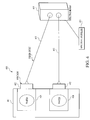
- system 400 includes wafer tool 401 within which the PECVD runs take place and a spectrometer 405 configured to collect spectral data indicative of the light emitted by the plasma during the PECVD runs, via one or more optical fibers 403 .
- System 400 may also include a spectral modeler 411 configured to store and analyze the spectral data collected by spectrometer 405 .
- a pair of chambers 406 may be provided.
- Each chamber includes a window 402 through which light emitted by respective plasma of a PECVD run may be observed.
- Window 402 is preferably made of quartz, which is highly transmissive through a wide range of photon wavelengths (e.g., 200 nm ⁇ 850 nm).
- One end of optical fiber 403 is attached to one of windows 402 to collect light emitted by plasma.
- the other end of optical fiber 403 is attached to spectrometer 405 .
- wafer tool 401 is an Applied Materials 200 mm Producer system.
- spectrometer 405 can be any commercially available spectrometer.
- An example is a spectrometer manufactured by OceanOptics, Inc., of Dunedin, Fla., which focuses the light on a blazed reflection grating (e.g., OceanOptics grating #10) that includes 1800 lines/mm and a specific spectral response.
- the light emitted by the plasma is wavelength dispersed and focused onto a 2048 linear Charge Coupled Device (CCD) array. Note that the dispersion is wavelength dependent with a greater spectral resolution near 850 nm than near 200 nm.
- CCD Charge Coupled Device
- Spectrometer 405 is used to capture the light emitted during the PECVD runs and generate spectral data. It should be noted that any spectrometer is sufficient for the purpose of the present invention as long as it is configured to have similar characteristics as that described above.
- spectral data analysis procedures can be done manually and/or using software program(s).
- the collected spectral data may be displayed on a computer display monitor (or used as input for an analysis program) in a number of different ways to provide different perspective of the collected spectral data.
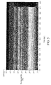
- Example display methods may include: graphically displaying three-dimensional spectral data (wavelength on the vertical axis vs. time on the horizontal axis vs. intensity displayed as gray level variation, FIG. 5); graphically displaying total time-dependent aspects of the spectral data (i.e., the sum of the spectral data in all 2048 CCD channels recorded each second, FIG. 6); graphically displaying spectral data captured by an individual CCD channel per second (FIG.
- spectral data can be collected using various techniques.
- One collection technique contemplated by at least some embodiments of the present invention is described below in connection with the collection of three-dimensional (intensity vs. wavelength vs. time) spectral data.
- Such data may be collected by spectrometer 405 during a modeling run using, e.g., an SiO 2 deposition recipe in the following manner. After a plasma is ignited in one or both of the chambers 406 , spectrometer 405 starts to collect spectral data when the intensity of the plasma emission reaches a pre-set threshold value.
- the CCD of spectrometer 405 is exposed to the light emitted by the plasma for 163 ms at a time, and raw spectral data during the exposure is recorded. Each second, six of these raw spectral data are averaged to produce a spectral data entry. For a run that has, for example, a 60 second duration, sixty spectral data entries are recorded during each PECVD run with a temporal resolution of one spectral data entry per second. At the end of the 60-second process the plasma is switched off and ten seconds of dark spectral data can be recorded in the same manner.
- the dark spectral data can be used as a background subtraction value during the spectral analyses in which the background subtraction value is subtracted from the spectral data collected during the PECVD runs. It should be noted that the above-described data collection procedure is provided only as an example. Accordingly, specific data collection timing and mechanism are not critical to embodiments of the present invention.
- another part of the preliminary analysis as contemplated by at least some embodiments of the present invention includes analyzing the spectral data collected during the center point runs. This analysis establishes a baseline against which changes observed in the spectral data of the various non-center point recipes can be compared. This analysis may begin with characterization of the time-dependent behavior of the total emission (the sum of the intensities recorded in the 2048 CCD pixels each second, FIG. 8) and the time-dependent behavior of individual spectral bands (the intensity recorded in individual pixels each second) as exemplified in FIG. 9.
- the characterization of the time dependent behavior of the total emission may involve measuring the magnitude of the total emission observed as a function of time and noting any structure in the spectral data.
- FIG. 6 shows a typical total spectral data trace (the sum of the spectral data in all of the 2048 CCD channels plotted every second). It may also be observed (as was the case in an example herein) that the spectral data begins with a value of about 5.25 ⁇ 10 4 au and decays to a value of about 5.15 ⁇ 10 4 au near the end of the run (see FIG. 6).
- the main result from the characterization of the time dependent behavior of the total run is that, in general, the total observed emission shows a slight decrease (1 to 2%) over the course of the run.
- the characterization of the time-dependent behavior of the center point runs may involve the characterization of the time-dependent behavior of individual spectral bands.
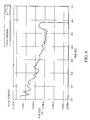
- FIG. 7 shows typical spectral data for a range of wavelengths.
- the trace line shown in FIG. 8 is the dominant line in the spectral data that occurs at the wavelength of ⁇ ⁇ 336.66 nm. Two different behaviors are observed in the spectral data.
- the first behavior is the ⁇ 1% periodic oscillation of the spectral data. This behavior is consistent with interference fringes arising from the interaction of light reflecting from the substrate of the wafer undergoing the PECVD runs and the surface of the growing film during the PECVD run. As the film grows, the increasing thickness of the film causes the reflected light to add alternatively (e.g., constructively and destructively) as a function of time, giving rise to the fringe pattern. It follows that the light received by spectrometer 405 originates from two main sources: the light emitted by the plasma directly into spectrometer 405 and the light reflected from the surface of the wafer.
- the interference fringes correspond to only a ⁇ 1% component of the collected spectral data.
- the second behavior noted in the wavelength traces is that the values of the spectral data decay for the first 30 seconds of the runs and then plateau for the final 30 seconds.
- This behavior may result because the light is reflected from two components.
- the first component is the light that is reflected from the substrate and the second component is the light that is reflected from the surface of the growing film. If the substrate is more reflective than the film, the intensity of the reflected component of the light may decrease with time as the film grows. When the film becomes sufficiently thick, the values of the spectral data plateau because the component reflected from the substrate is minimized.
- a prediction of this model is that the interference fringes should disappear as the light reflected from the substrate is minimized. Therefore, it is expected that all traces decrease by about the same amount if the chamber and process conditions are equivalent for each run.
- a number of spectral bands are formed by combining the collected spectral data from a range of wavelengths (step 205 ).
- FIGS. 9 - 13 show sections of collected spectral data of a typical center point run. The full spectrum covers the range from 250 nm ⁇ 800 nm. The spectral data shown are normalized to the value of the dominant line in the spectral data which, in this example, occurs at ⁇ ⁇ 336.66 nm.
- Example spectral bands are identified in the spectral data and are presented in Table 2. More specifically, each band is defined as those wavelengths existing between the “initial” and “final” wavelengths.
- spectral data corresponding to each formed spectral band is calculated, categorized, and analyzed (steps 207 , 209 and 211 ).
- the categorization and analysis are conducted according to the number of control parameters changed from those of the center point recipe.
- the spectral data collected when the setting of one control parameter is changed is categorized and analyzed together (step 207 ).
- the spectral data when the settings of two control parameters are changed is categorized and analyzed together (step 209 ) and so on.
- the following section describes the process of categorizing and analyzing the spectral data when the setting of one control parameter is changed, but similar analysis may be conducted for the spectral data collected when more than one parameter is changed.
- Spectral data collected during each example one-parameter 10% PECVD run is compared with the spectral data collected during the center point PECVD runs. By this comparison, the effect that each of the control parameters has on the optical emission spectra of process plasmas may then be determined.
- Table 3 shows the results of examining the spectral data to characterize the effects of five example control parameters on the individual spectral bands in the 1-parameter 10% PECVD runs. The 730-780 nm bands in each of the collected spectral data were normalized, since this band shows the least sensitivity to varying the settings on control parameters. Increases or decreases in the band intensities are then noted. Seven different symbols are used in the table:
- a diagnostic ratio is an equation derived based on, at least in part, the above described observations in order to adjust the control parameters. Table 3 shows that almost all of the spectral bands are sensitive to the N 2 O flow. Hence, the diagnostic ratio would be at least somewhat sensitive to the N 2 O flow.
- FIG. 14 shows the results of taking an example diagnostic ratio calculated by summing the spectral data of the 392.6-395.1 nm, 395.5-401.5 nm, 401.5-408 nm, 430.2-437 nm, and 445.1-450.06 nm bands, dividing the sum by the spectral data of the 421.3-430.2 band, and then, subtracting therefrom the value obtained by dividing the spectral data of the 416-421 nm band by the 421.3-430.2 nm band.
- This diagnostic ratio is chosen because the intensities of the five bands in the numerator of the first term are decreased for the high pressure and increased for the low pressure, while the intensities of the last two bands are increased for the high pressure and decreased for the low pressure.
- the bands show the opposite behaviors for the N 2 O flows. However, several of the bands do not show a change for the low N 2 O flow. Hence, the diagnostic ratio may not be as strong for the N 2 O flow as it is for the pressure.
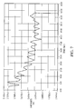
- the diagnostic ratio is calculated as described above and plotted as shown in FIG. 14.
- the plotted points located between 2.1 and 2.2 of the Y-axis represent the diagnostic ratios calculated for center point runs.
- the plotted points having the Y-axis value greater than 2.3 represent runs in which the pressure was set too high, and the plotted points having the Y-axis value smaller than 2.0 represent runs in which the pressure was set too low.
- the plotted points having the Y-axis value between 2.2 to 2.3 represent runs in which the N2O flow was set too low, and the plotted points having the Y-axis value between 2.0 and 2.1 represent N2O flow was set too high.
- FIG. 15 shows results of a diagnostic ratio of the sum of the spectral data the 386-392.5 nm, the 395-401.5 nm, and to the 430-437 nm bands.
- the runs shown in white are the runs in which both parameters were modified.
- the above-described diagnostic ratio is more sensitive to the electrode spacing being too small than it is to the spacing being too large.
- the ratio becomes more sensitive the more the spacing is out of the center point recipe.
- the plotted points located between 4.8 and 5.2 represent runs in which the electrode spacing was set too narrowly. This ratio appears to be somewhat sensitive to the N 2 O flow, but not as sensitive as the previous ratio. Nevertheless, the spacing of the electrodes dominates when both parameters are modified simultaneously. Note also that this ratio is not sensitive to the deposition of the film on the window.
- the conventional methods of determining diagnostic ratios proceed by first identifying the spectral bands that corresponding to major emission bands in the spectral data. Spectral data that originate from identified spectral bands are then used in a statistical analysis to correlate the spectral data with particular properties of run results using a simple linear model such as follows:
- I i represents absolute values of the spectral data of the identified spectral bands
- a i represents the coefficients derived by the statistical mapping model
- n is the number of bands used in the model.
- a drawback of this conventional method is that using the absolute values of the spectral data of the spectral bands requires a precise calibration of the entire data collection system.
- Several events that are likely to occur in the production environment would require a recalibration of the data collection system. These events include, for example, drifting control parameters, a change in substrate parameters resulting in a change in substrate reflectivity, clouding of the chamber window due to deposition of a film, and/or degrading optical fibers.
- R i represents ratios of bands.
- the ratio can be formed by using reactive bands and non-reactive bands, which are determined by noting the bands that were the most and least sensitive to changes to the settings of the control parameters.
- Eq. 1 is a generalized mathematical formulation of the example diagnostic ratio discussed above in connection with FIGS. 14 - 15 .
- the form of the ratios may depend on the collected spectral data. Using a model based on spectral ratios rather than the absolute intensities of spectral bands overcomes the need for an absolute calibration of the data collection system since one is only concerned with the relative intensities of the spectral data and not their absolute values. In fact, the diagnostic ratios are widely applicable for characterizing more than just the film properties. One may also characterize the process status, the chamber status, the spectrometer status and the like.
- modeling step 101 is completed when the diagnostic ratios are determined. Subsequently, one or more diagnostic ratios are used in monitoring and controlling steps (steps 103 and 105 , respectively). Although these steps are shown in a sequence, aspects of these steps may be performed separate from (e.g., in parallel with) each other. These steps can be executed using a monitoring and controlling system.
- FIG. 16 illustrates an example monitoring and controlling system that includes wafer tool 401 (with one more chambers), spectrometer 405 , spectral analyzer 1605 and control interface 1601 .
- Wafer tool 401 is coupled with spectrometer 405 as described above in connection with FIG. 4.
- Spectral analyzer 1605 is coupled with spectrometer 405 and control interface 1607 .
- the example monitoring and controlling system includes a number of wafer tools 401 and support devices (e.g., optical cables) to be used in a manufacturing facility.
- Spectral analyzer 1607 includes the features of spectral modeler 411 described above in connection with FIG. 4. Accordingly, the diagnostic ratios described above are stored in spectral analyzer 1605 . In addition, spectral analyzer 1605 is further configured to communicate with control interface 1607 with its communication interface.
- wafer tool 401 and, spectrometer 405 function substantially similar as described above.
- the monitoring step is performed by spectrometer 405 and spectral analyzer 1605 . More specifically, during the monitoring step, spectral data of plasma activities in the chamber(s) of wafer tool 401 is collected and results of one or more selected diagnostic ratios are generated based on the collected spectral data.
- control signals based on the results of the selected diagnostic ratios are produced by spectral analyzer 1605 . For instance, if the results of the selected diagnostic ratios indicate that an excessive amount of gas is supplied, then spectral analyzer 1605 sends a control signal to control interface 1607 to decrease the gas supply to the corresponding chamber(s) of the wafer tool 401 . In turn, control interface 1607 physically carries out the instructions of the control signal. In this example, control interface 1607 would proportionally close a valve that supplies the gas to the corresponding chamber(s) of the wafer tool 401 .
- spectral data proportional to light emitted by plasma during a PECVD run is collected (step 1710 ).
- the collected data is processed in real time to generate the results of the selected diagnostic ratios (step 1720 ).
- one or more the control parameters are modified to ensure that the PECVD run would be performed close to its center point recipe (step 1730 ).
- FIG. 18 illustrates a block diagram of one example of the internal hardware of spectral modeler 411 .
- a bus 1856 serves as the main information highway interconnecting various components of analyzer 1605 .
- CPU 1605 is the central processing unit of the analyzer, performing calculations and logic operations required to execute the processes of the present invention as well as other programs.
- Read only memory (ROM) 1860 and random access memory (RAM) 1862 constitute the main memory of modeler 1811 .
- Disk controller 1864 interfaces one or more disk drives to the system bus 1856 . These disk drives are, for example, floppy disk drives 1870 , or CD ROM or DVD (digital video disks) drives 1866 , or internal or external hard drives 1868 . These various disk drives and disk controllers are optional devices.
- a display interface 1872 interfaces display 1848 and permits information from the bus 1856 to be displayed on display 1848 .
- Display 1848 may be used in displaying various graphs as shown in FIGS. 5 - 15 .
- Communications with external devices such as the other components of the system described above, occur utilizing, for example, communication port 1874 .
- Optical fibers and/or electrical cables and/or conductors and/or optical communication e.g., infrared, and the like
- wireless communication e.g., radio frequency (RF), and the like
- Peripheral interface 1854 interfaces the keyboard 1850 and mouse 1852 , permitting input data to be transmitted to bus 1856 .
- the analyzer also optionally includes an infrared transmitter and/or infrared receiver.
- Infrared transmitters are optionally utilized when the computer system is used in conjunction with one or more of the processing components/stations that transmits/receives data via infrared signal transmission.
- the computer system may also optionally use a low power radio transmitter 1880 and/or a low power radio receiver 1882 .
- the low power radio transmitter transmits the signal for reception by components of the production process, and receives signals from the components via the low power radio receiver.
- the low power radio transmitter and/or receiver are standard devices in industry.
- the analyzer in FIG. 18 is illustrated having a single processor, a single hard disk drive and a single local memory, the analyzer is optionally suitably equipped with any multitude or combination of processors or storage devices.
- the analyzer may be replaced by, or combined with, any suitable processing system operative in accordance with the principles of embodiments of the present invention, including sophisticated calculators, and hand-held, laptop/notebook, mini, mainframe and super computers, as well as processing system network combinations of the same.
- FIG. 19 is an illustration of an example computer readable memory medium 1984 utilizable for storing computer readable code or instructions.
- medium 1984 may be used with disk drives illustrated in FIG. 18.
- memory media such as floppy disks, or a CD ROM, or a digital video disk will contain, for example, a multi-byte locale for a single byte language and the program information for controlling the modeler to enable the computer to perform the functions described herein.
- ROM 1860 and/or RAM 1862 illustrated in FIG. 18 can also be used to store the program information that is used to instruct the central processing unit 1858 to perform the operations associated with various automated processes of the present invention.
- suitable computer readable media for storing information include magnetic, electronic, or optical (including holographic) storage, some combination thereof, etc.
- FIGS. 18 and 19 are related to only one set of wafer tool, spectrometer, spectral analyzer and control interface, it may be used in a manufacturing run, as noted above. Furthermore, the spectrometer and spectral analyzer and control interface may be provided for each chamber of wafer tools. In an alternative embodiment, one spectrometer may be provided for many wafer tools. Similarly, one spectral analyzer may be provided for many chambers of wafer tools and/or many spectrometers.
Landscapes
- Chemical & Material Sciences (AREA)
- Engineering & Computer Science (AREA)
- Metallurgy (AREA)
- Chemical Kinetics & Catalysis (AREA)
- Materials Engineering (AREA)
- Mechanical Engineering (AREA)
- General Chemical & Material Sciences (AREA)
- Organic Chemistry (AREA)
- Physics & Mathematics (AREA)
- Plasma & Fusion (AREA)
- Analytical Chemistry (AREA)
- Drying Of Semiconductors (AREA)
- Chemical Vapour Deposition (AREA)
Abstract
A method, system, and medium of spectroscopically modeling and/or controlling a semiconductor manufacturing process. The modeling/controlling includes the steps of conducting a plurality of semiconductor manufacturing process runs by changing at least one of process parameters from its target value, and collecting spectral data indicative of the light emitted by plasma during each of said semiconductor manufacturing process runs. The modeling/controlling also includes the step of formulating a ratio based on a relationship between the collected spectral data and the changes in the at least one of the plurality of process parameters.
Description
- The present invention relates to enhancing process control of plasma based semiconductor manufacturing processes. In particular, at least some embodiments of the present invention relate to modeling and monitoring light spectra emitted by the plasma of a plasma based semiconductor manufacturing process and control the plasma based process based on the light spectra.
- A “plasma based semiconductor process” generally refers to a methodology for fabricating microelectronic devices such as very large scale integration (VLSI) microelectronic chips and/or thin film transistors (TFTs). In particular, plasma based semiconductor processes may be used, for example, in deposition processes (e.g., plasma enhanced chemical vapor deposition, hereinafter “PECVD”) and/or etching processes during the fabrication of microelectronic devices.
- For example, a PECVD run (a particular instance of conducting a PECVD process) includes the following steps: 1) a device to be processed is placed within a chamber; 2) an initial condition is created inside the chamber using control parameters (e.g., RF power, electrode spacing, gas pressure, SiH 4 flow, N2O flow, etc.); 3) plasma is ignited; 4) the control parameters are adjusted; 5) a desired end point (e.g., a predetermined thickness of a film being deposited) is reached; and 6) the run is then terminated.
- During a PECVD run, diagnosis and proper process control of the PECVD run are desired in order to ensure that microelectronic devices produced by the PECVD run are free of defects. The diagnostics and proper process control may be provided manually or automatically in order to determine when an end point has been reached in order to adjust the control parameters while the PECVD run is in progress.
- A first group of conventional methods for controlling a PECVD run focus on determining when its end point is reached. There are three general techniques in this group of conventional methods: (1) optical end point; (2) interferometric end point; and (3) test wafer measurement.
- The optical end point technique involves determining the end point of a PECVD run by monitoring one or two narrow spectral bands of spectral emission from the plasma of the PECVD run. This technique is generally not predictive. In particular, use of this technique does not adequately permit detection of an approaching end point. Thus, a PECVD run must first come to its end point before the end point is observed by this technique, which almost always causes delays in terminating the PECVD run (which, e.g., can then result in the endpoint being overshot). While these shortcomings may be overlooked in experimental PECVD runs, they may cause unacceptable level of errors should this technique be used in manufacturing processes.
- The interferometric end point technique also attempts to determine the end point, but uses interferometric interference fringes as a measurement. However, a number of different types of material (e.g., metal) do not show the interferometric interference fringes unless the film deposited by the PECVD run is extremely thin. Hence, this technique may not be viable for depositing metal films. In addition, similar to the optical end point technique described above, the interferometric technique does not predict the end points, thereby causing delays in stopping a PECVD run when its end point is reached.
- The test wafer measurement technique involves determination of the quality of microelectronic devices by physically examining one or more microelectronic devices per a batch of manufactured microelectronic devices. Each time a test microelectronic device is examined and passes a minimum standard (e.g., is determined to be within a predetermined range of the end point thickness), it acts as a certification that microelectronic devices of the batch may also meet the minimum standard. However, when a test microelectronic device fails to meet the minimum standard, each and every one of the microelectronic devices of that batch must be discarded or individually tested, which is an expensive process because each microelectronic device may be worth many tens of thousands of dollars. Another drawback of this technique is the fact that many of the quality tests are destructive in nature.
- In addition to the deficiencies mentioned above, the above described conventional techniques of process control cannot detect a PECVD run that has gone out of optimal process specifications (e.g., overshot the optimal thickness of the deposition film) while the process is ongoing. In addition, these techniques do not provide steps that are necessary to correct erroneous processes.
- In order to reduce some of the shortcomings of the above-described techniques, a second group of conventional techniques have also been developed. This group of conventional techniques does not focus on determining when the end points have been reached as in the first conventional techniques. Instead, the second group monitors ongoing processes. An example of such techniques involves monitoring the control parameters. This technique has shown some success in predicting film properties for PECVD runs, but it is still relatively inaccurate in determining the end points because this technique relies only on the control parameters without monitoring the actual PECVD run (e.g., without monitoring the progress of the device being produced).
- Thus, what is needed is a scheme to better control semiconductor processes so that, e.g., the quality of fabricated microelectronic devices will increase.
- Embodiments of the present invention advantageously overcome the above described shortcomings of the aforementioned techniques. In particular, embodiments of the present invention provide a system, method and medium for modeling, monitoring, and/or controlling plasma based semiconductor manufacturing processes. For instance, in at least some embodiments of the present invention, a method of modeling/controlling a plasma based semiconductor manufacturing process includes the steps of conducting a plurality of semiconductor manufacturing process runs by changing at least one of process parameters from its target value, and collecting spectral data indicative of the light emitted by plasma during each of said semiconductor manufacturing process runs. The modeling/controlling also includes the step of formulating a ratio based on a relationship between the collected spectral data and the changes in the at least one of the plurality of process parameters.
- The detailed description of the present application showing various distinctive features may be best understood when the detailed description is read in reference to the appended drawing in which:
- FIG. 1 is a high-level flow chart representation of example primary steps as contemplated by at least some embodiments of the present invention;
- FIG. 2 is a flow chart representation of example steps in modeling a PECVD recipe;
- FIG. 3 is a flow chart representation of an example modeling run of the present invention;
- FIG. 4 is a top view of an example setup for the modeling run of the present invention;
- FIG. 5 is a graph representing a three-dimensional spectrum for an example PECVD run;
- FIG. 6 is a graph representing a trace of total intensity of an example PECVD run;
- FIG. 7 is a graph representing a trace of intensity at a certain wavelength of an example PECVD run;
- FIG. 8 is a graph representing intensity of a section of a spectrum at a give time of an example PECVD run;
- FIG. 9 is a graph representing a trace of the 200 nm-300 nm section of an example center point spectrum;
- FIG. 10 is a graph representing a trace of the 300 nm-387 nm section of an example center point spectrum;
- FIG. 11 is a graph representing a trace of the 387 nm-437 nm section of an example center point spectrum;
- FIG. 12 is a graph representing a trace of the 437 nm-530 nm section of an example center point spectrum;
- FIG. 13 is a graph representing a trace of the 530 nm-800 nm section of an example center point spectrum;
- FIG. 14 is a diagram representing a plot of results obtained using a first diagnostic ratio;
- FIG. 15 is a diagram representing a plot of results obtained using a second diagnostic ratio;
- FIG. 16 is a schematic diagram representing a controlling system of at least some embodiments contemplated by the present invention;
- FIG. 17 is a flow chart representing the steps in controlling a PECVD process of the present invention;
- FIG. 18 is a block diagram representation of an example embodiment of a spectral modeler; and
- FIG. 19 illustrates one example of a memory medium which may be used for storing the spectral modeler of the present invention.
- Embodiments of the present invention provide proper diagnostics and/or process control to plasma based semiconductor manufacturing processes by conducting one or more of the high-level steps indicated in FIG. 1. Referring now to FIG. 1, these steps include modeling, monitoring, and controlling the plasma based semiconductor manufacturing processes (
steps - In the modeling step (step 101), characteristics of PECVD runs of a particular recipe are determined. A recipe is a set of control settings for control parameters such as specified ranges and application length of time. Examples of control parameters include RF power, electrode spacing, gas pressure, SiH4 flow, and N2O flow. Thus, for instance, a recipe may specify how much RF power to apply and for how long during a PECVD run. A run is one specific instance of processing a wafer using a specified recipe.
- Detail processes of the modeling step, which includes a number of sub-steps, are described with regard to FIG. 2. Referring now to FIG. 2, a number of PECVD runs are conducted by varying control parameters (step 201). While the PECVD runs are being conducted, spectral data is collected. The collected spectral data is indicative of (e.g., is proportional to) the light emitted by plasma during each of the PECVD runs (step 203). After the spectral data is collected and analyzed, a number of spectral bands are formed (step 205). Subsequently, the collected spectral data is categorized for each formed spectral band (
steps - In context of
modeling step 101, the step of conducting a number of PECVD runs (step 201) can be thought of as executing a modeling run. A modeling run may include a series of PECVD runs where the control settings of one or more control parameters are varied from a center point PECVD recipe. A center point recipe (also referred to as a target process) is a set of optimally designed control settings (also referred to as target values) for each of the control parameters to achieve a specific goal. For instance, a center point recipe designed to etch a layer may specify one set of optimal control settings. It should be noted that at least some embodiments of the present invention are directed to recipes other than PECVD. In such embodiments, their center point recipe may be designed to deposit a layer (e.g., a film) by using a corresponding set of optimal control settings. A non-center point recipe is a recipe that includes different control settings for one or more control parameters from those of the center point recipe. - An example modeling run for an optimal SiO 2 deposition recipe may include a number of different PECVD runs as follows: a center point run in which all control parameters are set to their optimal values and a number of non-center point runs in which the setting of one control parameter at a time is varied by plus/minus a predetermined percentage (e.g., 5% or 10%) over its optimal value. The variation on the settings of the control parameters can be any value as long as the variation is sufficient to cause an observable change in the collected spectral data. The number of the non-center point runs can be equal to, e.g., two times the number of control parameters when the settings of control parameters are changed one at a time.
- Another example modeling run is described with regard to FIG. 3). Referring now to FIG. 3, this example modeling run contemplates the following: forty-six PECVD runs that consist of forty-one 2-
parameter 10% PECVD runs (i.e., the settings of control parameters are changed two at a time, and are varied ±10% from the value of the center point run) with five center point runs dispersed randomly throughout (step 301); eight 5-parameter 5% PECVD runs (i.e., the settings of five control parameters are changed) (step 303); ten 1-parameter 10% PECVD runs (step 305); and eleven center point runs (step 307). Six more center point runs (step 309) also may be conducted after cleaning the system within which the runs are conducted (step 308). It should be noted that the above-discussed modeling run is merely an example contemplated by at least some embodiments of the present invention, and that any other number of PECVD runs and/or combination of variations to the settings of the control parameters of the center point recipe are also envisioned by the present invention. - Table 1 illustrates detailed information on a modeling run similar to the above example modeling run of FIG. 3. In Table 1, a sequence of symbols such as “++ . . . ” in the “Pattern ” column designates that the first two parameters (i.e., pressure and electrode spacing) are increased while the last three parameters (i.e., power, SiH 4 and N2O) are decreased. Similarly the sequence of symbols “00-00” designates that the third parameter is decreased while the rest of parameters are not changed. Since each run processes a wafer, the runs are referenced using wafer numbers in Table 1.
TABLE 1 Center Point (CP) values below. Pressure Spacing Power SiH4 N2O 1. Perform chamber conditioning. Obtain CP values. CP 2.70 500 315.0 260 3500 Calculated 10% and 5% values (enter any other value below if calculated value is not desired): +10% 2.97 550 347.0 286 3850 −10% 2.43 450 283.0 234 3150 +5% 2.84 525 331.0 273 3675 −5% 2.57 475 299.0 247 3325 Wafer Pattern Pressure Spacing Power SiH4 N2O 2. Run 46 wafers according to the following 10% recipe. 1 00000 2.70 500 315.0 260 3500 2 000++ 2.70 500 315.0 286 3850 3 0+−00 2.70 550 283.0 260 3500 4 00000 2.70 500 315.0 260 3500 5 00000 2.70 500 315.0 260 3500 6 −+000 2.43 550 315.0 260 3500 7 0−00− 2.70 450 315.0 260 3150 8 −0+00 2.43 500 347.0 260 3500 9 0−+00 2.70 450 347.0 260 3500 10 +000− 2.97 500 315.0 260 3150 11 0+00+ 2.70 550 315.0 260 3850 12 0−−00 2.70 450 283.0 260 3500 13 00000 2.70 500 315.0 260 3500 14 00−0+ 2.70 500 283.0 260 3850 15 −0−00 2.43 500 283.0 260 3500 16 +0+00 2.97 500 347.0 260 3500 17 000−+ 2.70 500 315.0 234 3850 18 0−00+ 2.70 450 315.0 260 3850 19 0+0−0 2.70 550 315.0 234 3500 20 0+0+0 2.70 550 315.0 286 3500 21 +00−0 2.97 500 315.0 234 3500 22 00000 2.70 500 315.0 260 3500 23 +−000 2.97 450 315.0 260 3500 24 0−0+0 2.70 450 315.0 286 3500 25 00−0− 2.70 500 283.0 260 3150 26 000+− 2.70 500 315.0 286 3150 27 +000+ 2.97 500 315.0 260 3850 28 00−+0 2.70 500 283.0 286 3500 29 −00−0 2.43 500 315.0 234 3500 30 −−000 2.43 450 315.0 260 3500 31 ++000 2.97 550 315.0 260 3500 32 00++0 2.70 500 347.0 286 3500 33 +00+0 2.97 500 315.0 286 3500 34 +0−00 2.97 500 283.0 260 3500 35 000−− 2.70 500 315.0 234 3150 36 00+0− 2.70 500 347.0 260 3150 37 00+0+ 2.70 500 347.0 260 3850 38 −000− 2.43 500 315.0 260 3150 39 0+00− 2.70 550 315.0 260 3150 40 00+−0 2.70 500 347.0 234 3500 41 −000+ 2.43 500 315.0 260 3850 42 −00+0 2.43 500 315.0 286 3500 43 00−−0 2.70 500 283.0 234 3500 44 0++00 2.70 550 347.0 260 3500 45 00000 2.70 500 315.0 260 3500 46 0−0−0 2.70 450 315.0 234 3500 3. Run 8 wafers according to the following 5% recipe. 47 +−+−− 2.84 475 331.0 247 3325 48 −−++− 2.57 475 331.0 273 3325 49 −++−+ 2.57 525 331.0 247 3675 50 +−−++ 2.84 475 299.0 273 3675 51 −−−−+ 2.57 475 299.0 247 3675 52 +++++ 2.84 525 331.0 273 3675 53 −+−+− 2.57 525 299.0 273 3325 54 ++−−− 2.84 525 299.0 247 3325 4. Run 10 wafers varying one parameter at a time as follows.55 +0000 2.97 500 315.0 260 3500 56 −0000 2.43 500 315.0 260 3500 57 0+000 2.70 550 315.0 260 3500 58 0−000 2.70 450 315.0 260 3500 59 00+00 2.70 500 347.0 260 3500 60 00−00 2.70 500 283.0 260 3500 61 000+0 2.70 500 315.0 286 3500 62 000−0 2.70 500 315.0 234 3500 63 0000+ 2.70 500 315.0 260 3850 64 0000− 2.70 500 315.0 260 3150 Run 10 wafers at CP.65 to 74 00000 2.70 500 315.0 260 3500 - The above described modeling run and the step of collecting spectral data (step 203) can be carried out in a spectral data collection system, such as the one illustrated in FIG. 4. Referring first to FIG. 4,
system 400 includeswafer tool 401 within which the PECVD runs take place and aspectrometer 405 configured to collect spectral data indicative of the light emitted by the plasma during the PECVD runs, via one or moreoptical fibers 403.System 400 may also include aspectral modeler 411 configured to store and analyze the spectral data collected byspectrometer 405. - As shown in FIG. 4, a pair of
chambers 406 may be provided. Each chamber includes awindow 402 through which light emitted by respective plasma of a PECVD run may be observed.Window 402 is preferably made of quartz, which is highly transmissive through a wide range of photon wavelengths (e.g., 200 nm<λ<850 nm). One end ofoptical fiber 403 is attached to one ofwindows 402 to collect light emitted by plasma. The other end ofoptical fiber 403 is attached tospectrometer 405. In at least some embodiments of the present invention,wafer tool 401 is an Applied Materials 200 mm Producer system. - In at least some embodiments of the present invention,
spectrometer 405 can be any commercially available spectrometer. An example is a spectrometer manufactured by OceanOptics, Inc., of Dunedin, Fla., which focuses the light on a blazed reflection grating (e.g., OceanOptics grating #10) that includes 1800 lines/mm and a specific spectral response. The light emitted by the plasma is wavelength dispersed and focused onto a 2048 linear Charge Coupled Device (CCD) array. Note that the dispersion is wavelength dependent with a greater spectral resolution near 850 nm than near 200 nm. Another example is a portable Verity™ spectrometer system that includes the above described spectrometer integrated with control software.Spectrometer 405 is used to capture the light emitted during the PECVD runs and generate spectral data. It should be noted that any spectrometer is sufficient for the purpose of the present invention as long as it is configured to have similar characteristics as that described above. - Once the spectral data for the modeling run has been collected, a preliminary analysis of the spectral data can be conducted (and can be thought of as part of, e.g., step 203). The following steps describe spectral data analysis procedures that can be done manually and/or using software program(s).
- In one instance of the preliminary analysis, the collected spectral data may be displayed on a computer display monitor (or used as input for an analysis program) in a number of different ways to provide different perspective of the collected spectral data. Example display methods may include: graphically displaying three-dimensional spectral data (wavelength on the vertical axis vs. time on the horizontal axis vs. intensity displayed as gray level variation, FIG. 5); graphically displaying total time-dependent aspects of the spectral data (i.e., the sum of the spectral data in all 2048 CCD channels recorded each second, FIG. 6); graphically displaying spectral data captured by an individual CCD channel per second (FIG. 7); graphically displaying spectral data at a given time (i.e., the intensity in each of the 2048 CCD channels at a particular time, FIG. 8); and, graphically displaying time-averaged spectral data (i.e., the average spectral data recorded in each of the 2048 CCD channels for the 60 second processes).
- The above-described spectral data can be collected using various techniques. One collection technique contemplated by at least some embodiments of the present invention is described below in connection with the collection of three-dimensional (intensity vs. wavelength vs. time) spectral data. Such data may be collected by
spectrometer 405 during a modeling run using, e.g., an SiO2 deposition recipe in the following manner. After a plasma is ignited in one or both of thechambers 406,spectrometer 405 starts to collect spectral data when the intensity of the plasma emission reaches a pre-set threshold value. In the example data collection procedure, while the PECVD runs are being conducted, the CCD ofspectrometer 405 is exposed to the light emitted by the plasma for 163 ms at a time, and raw spectral data during the exposure is recorded. Each second, six of these raw spectral data are averaged to produce a spectral data entry. For a run that has, for example, a 60 second duration, sixty spectral data entries are recorded during each PECVD run with a temporal resolution of one spectral data entry per second. At the end of the 60-second process the plasma is switched off and ten seconds of dark spectral data can be recorded in the same manner. The dark spectral data can be used as a background subtraction value during the spectral analyses in which the background subtraction value is subtracted from the spectral data collected during the PECVD runs. It should be noted that the above-described data collection procedure is provided only as an example. Accordingly, specific data collection timing and mechanism are not critical to embodiments of the present invention. - As can be appreciated by the previous discussions, another part of the preliminary analysis as contemplated by at least some embodiments of the present invention includes analyzing the spectral data collected during the center point runs. This analysis establishes a baseline against which changes observed in the spectral data of the various non-center point recipes can be compared. This analysis may begin with characterization of the time-dependent behavior of the total emission (the sum of the intensities recorded in the 2048 CCD pixels each second, FIG. 8) and the time-dependent behavior of individual spectral bands (the intensity recorded in individual pixels each second) as exemplified in FIG. 9.
- The characterization of the time dependent behavior of the total emission may involve measuring the magnitude of the total emission observed as a function of time and noting any structure in the spectral data. FIG. 6 shows a typical total spectral data trace (the sum of the spectral data in all of the 2048 CCD channels plotted every second). It may also be observed (as was the case in an example herein) that the spectral data begins with a value of about 5.25×10 4 au and decays to a value of about 5.15×10⁴ au near the end of the run (see FIG. 6). The main result from the characterization of the time dependent behavior of the total run is that, in general, the total observed emission shows a slight decrease (1 to 2%) over the course of the run.
- In addition, the characterization of the time-dependent behavior of the center point runs may involve the characterization of the time-dependent behavior of individual spectral bands. FIG. 7 shows typical spectral data for a range of wavelengths. The trace line shown in FIG. 8 is the dominant line in the spectral data that occurs at the wavelength of λ˜336.66 nm. Two different behaviors are observed in the spectral data.
- The first behavior is the ±1% periodic oscillation of the spectral data. This behavior is consistent with interference fringes arising from the interaction of light reflecting from the substrate of the wafer undergoing the PECVD runs and the surface of the growing film during the PECVD run. As the film grows, the increasing thickness of the film causes the reflected light to add alternatively (e.g., constructively and destructively) as a function of time, giving rise to the fringe pattern. It follows that the light received by
spectrometer 405 originates from two main sources: the light emitted by the plasma directly intospectrometer 405 and the light reflected from the surface of the wafer. (Note that it is also likely that reflection from the chamber walls and stray light fromwindow 402 may also contribute to the collected spectral data). Because the light directly emitted from the plasma constitutes the main component of the collected light rather than that reflected from the wafer surface, the interference fringes correspond to only a ±1% component of the collected spectral data. - The second behavior noted in the wavelength traces is that the values of the spectral data decay for the first 30 seconds of the runs and then plateau for the final 30 seconds. This behavior may result because the light is reflected from two components. As noted above, the first component is the light that is reflected from the substrate and the second component is the light that is reflected from the surface of the growing film. If the substrate is more reflective than the film, the intensity of the reflected component of the light may decrease with time as the film grows. When the film becomes sufficiently thick, the values of the spectral data plateau because the component reflected from the substrate is minimized. A prediction of this model is that the interference fringes should disappear as the light reflected from the substrate is minimized. Therefore, it is expected that all traces decrease by about the same amount if the chamber and process conditions are equivalent for each run.
- The above-described characterizations of the preliminary analysis are provided only as examples. Other observations and characterizations within the skill set of one of ordinary skill in the art are also contemplated within embodiments of the present invention.
- After the preliminary analysis (or after collecting the spectral data without performing the preliminary analysis), a number of spectral bands are formed by combining the collected spectral data from a range of wavelengths (step 205). For example, FIGS. 9-13 show sections of collected spectral data of a typical center point run. The full spectrum covers the range from 250 nm<λ<800 nm. The spectral data shown are normalized to the value of the dominant line in the spectral data which, in this example, occurs at λ˜336.66 nm. Example spectral bands are identified in the spectral data and are presented in Table 2. More specifically, each band is defined as those wavelengths existing between the “initial” and “final” wavelengths. It should be noted that the set of bands illustrated in Table 2 is provided only as an example. Different sets of bands can also be used as shown in, e.g., Table 3 below.
TABLE 2 λ0 [nm] λ(initial) λ(final) N/A 250 300 314 310 317 337 331 342 350 347 354 357 355 360 367 363 372 374 372 377 380 377 383 390 387 395 398 396 401 404 401 408 414 410 416 418 416 421 426 421 430 434 430 437 442 438 444 448 444 451 456 451 460 465 460 469 472 469 474 483 477 488 547 532 563 655 620 691 752 720 784 - Once spectral bands are determined, spectral data corresponding to each formed spectral band is calculated, categorized, and analyzed (
steps parameter 10% PECVD run is compared with the spectral data collected during the center point PECVD runs. By this comparison, the effect that each of the control parameters has on the optical emission spectra of process plasmas may then be determined. Table 3 shows the results of examining the spectral data to characterize the effects of five example control parameters on the individual spectral bands in the 1-parameter 10% PECVD runs. The 730-780 nm bands in each of the collected spectral data were normalized, since this band shows the least sensitivity to varying the settings on control parameters. Increases or decreases in the band intensities are then noted. Seven different symbols are used in the table: - significant increase in band intensity

- ↑ increase in band intensity
- minor increase in band intensity

- no effect

- minor decrease in band intensity

- ↓ decrease in band intensity
- significant decrease in band intensity

- It should be noted that, although Table 3 shows only qualitative measurements, using precise quantitative numbers is also contemplated within at least some embodiments of the present invention.
TABLE 3 Spectral Pressure Spacing Power SiH4 N2O Band (nm) Hi Lo Hi Lo Hi Lo Hi Lo Hi Lo 310-317 


332-338.5 


347.5-354.5 


354.6-360 


362.5-372.5 


372.5-376.8 


376.8-382 


386-392.5 


392.5-395 


395-401.5 


401.5-408 


410-416 


416-421 


421-430 


430-437 


438-444 


444-451 


451-460 


460-469 


469-474 


477-488 


488-496 


- In Table 3, it can be observed that three of the bands (395-401.5, 401.5-408, and 410-416) are all sensitive to pressure changes on and spacing of electrodes. In other words, when the pressure and spacing of electrodes change, corresponding spectral data in those bands also changes. In another example, for the electrode spacing, there are two bands (386-392.5 and 395-401.5) that are sensitive to distinguish two settings. More specifically, when the spacing is set to be large (the “Hi” setting), significant increase of intensities in those bands are observed; whereas, when the spacing is set to be small (the “Lo” setting) minor decreases of intensities in those bands are observed. Based on this analysis, when minor decreases of intensities in those bands are observed in future runs, such observations indicate that the spacing may be set too small. It also follows that, when significant increases of intensities in those bands are observed in future runs, such observations indicate that the spacing may be set too large. For the power, there is only one band (410-416) that is sensitive to distinguish two settings. The same band is also sensitive to the SiH 4 flow. For the N2O flow there are eight bands that are sensitive. These sensitive spectral bands are also referred as reactive bands because they show reaction to changing the settings of the control parameters.
- The above discussed observations on the spectral data changes caused by varying the settings on the control parameters may be used to determine diagnostic ratios (step 213). A diagnostic ratio is an equation derived based on, at least in part, the above described observations in order to adjust the control parameters. Table 3 shows that almost all of the spectral bands are sensitive to the N2O flow. Hence, the diagnostic ratio would be at least somewhat sensitive to the N2O flow.
- FIG. 14 shows the results of taking an example diagnostic ratio calculated by summing the spectral data of the 392.6-395.1 nm, 395.5-401.5 nm, 401.5-408 nm, 430.2-437 nm, and 445.1-450.06 nm bands, dividing the sum by the spectral data of the 421.3-430.2 band, and then, subtracting therefrom the value obtained by dividing the spectral data of the 416-421 nm band by the 421.3-430.2 nm band. This diagnostic ratio is chosen because the intensities of the five bands in the numerator of the first term are decreased for the high pressure and increased for the low pressure, while the intensities of the last two bands are increased for the high pressure and decreased for the low pressure. Note that the bands show the opposite behaviors for the N 2O flows. However, several of the bands do not show a change for the low N2O flow. Hence, the diagnostic ratio may not be as strong for the N2O flow as it is for the pressure.
- For each run, the diagnostic ratio is calculated as described above and plotted as shown in FIG. 14. In particular, the plotted points located between 2.1 and 2.2 of the Y-axis (i.e., the value of the diagnostic ratio) represent the diagnostic ratios calculated for center point runs. The plotted points having the Y-axis value greater than 2.3 represent runs in which the pressure was set too high, and the plotted points having the Y-axis value smaller than 2.0 represent runs in which the pressure was set too low. In addition, the plotted points having the Y-axis value between 2.2 to 2.3 represent runs in which the N2O flow was set too low, and the plotted points having the Y-axis value between 2.0 and 2.1 represent N2O flow was set too high.
- In another example ratio, FIG. 15 shows results of a diagnostic ratio of the sum of the spectral data the 386-392.5 nm, the 395-401.5 nm, and to the 430-437 nm bands. The runs shown in white are the runs in which both parameters were modified. The above-described diagnostic ratio is more sensitive to the electrode spacing being too small than it is to the spacing being too large. Note also that the ratio becomes more sensitive the more the spacing is out of the center point recipe. For instance, the plotted points located between 4.8 and 5.2 represent runs in which the electrode spacing was set too narrowly. This ratio appears to be somewhat sensitive to the N 2O flow, but not as sensitive as the previous ratio. Nevertheless, the spacing of the electrodes dominates when both parameters are modified simultaneously. Note also that this ratio is not sensitive to the deposition of the film on the window.
- Now turning to describe a general mathematical formulation to determine diagnostic ratios, a conventional method is first described below along with its shortcomings, and then, a different method contemplated by at least some embodiments of the present invention relating to the general mathematical formation of diagnostic ratios is described.
- In general, the conventional methods of determining diagnostic ratios proceed by first identifying the spectral bands that corresponding to major emission bands in the spectral data. Spectral data that originate from identified spectral bands are then used in a statistical analysis to correlate the spectral data with particular properties of run results using a simple linear model such as follows:
- Property=a 1 I 1 +a 2 I 2 + . . . +a n I n+const.
- where I i represents absolute values of the spectral data of the identified spectral bands, ai represents the coefficients derived by the statistical mapping model, and n is the number of bands used in the model. In general, the more bands that are used in the equation the more accurately the models reproduce observed film properties.
- A drawback of this conventional method is that using the absolute values of the spectral data of the spectral bands requires a precise calibration of the entire data collection system. Several events that are likely to occur in the production environment would require a recalibration of the data collection system. These events include, for example, drifting control parameters, a change in substrate parameters resulting in a change in substrate reflectivity, clouding of the chamber window due to deposition of a film, and/or degrading optical fibers.
- To best handle the non-predictive nature of the conventional techniques, one would need to either closely monitor chamber, process, optics, and spectrometer conditions to determine when a recalibration is necessary, or insert a calibration step between each process run, costing additional time and resources. Consequently, a calibration free solution would be desirable.
- Thus, at least some embodiments of the present invention contemplate employing simple linear relationships of spectral data as do the conventional system, but instead use ratios in its equation as illustrated in the diagnostic ratios discussed above in connection with FIGS. 14-15. In particular, the general mathematical formulation of embodiments the present invention is as follows:
- process parameters=a 1 R 1 +a 2 R 2 + . . . +a n R n+const. Eq. 1
- where R i represents ratios of bands. The ratio can be formed by using reactive bands and non-reactive bands, which are determined by noting the bands that were the most and least sensitive to changes to the settings of the control parameters. It should be noted that Eq. 1 is a generalized mathematical formulation of the example diagnostic ratio discussed above in connection with FIGS. 14-15.
- The form of the ratios may depend on the collected spectral data. Using a model based on spectral ratios rather than the absolute intensities of spectral bands overcomes the need for an absolute calibration of the data collection system since one is only concerned with the relative intensities of the spectral data and not their absolute values. In fact, the diagnostic ratios are widely applicable for characterizing more than just the film properties. One may also characterize the process status, the chamber status, the spectrometer status and the like.
- In at least some embodiments of the present invention, modeling
step 101 is completed when the diagnostic ratios are determined. Subsequently, one or more diagnostic ratios are used in monitoring and controlling steps (steps - FIG. 16 illustrates an example monitoring and controlling system that includes wafer tool 401 (with one more chambers),
spectrometer 405,spectral analyzer 1605 and control interface 1601.Wafer tool 401 is coupled withspectrometer 405 as described above in connection with FIG. 4.Spectral analyzer 1605 is coupled withspectrometer 405 andcontrol interface 1607. The example monitoring and controlling system includes a number ofwafer tools 401 and support devices (e.g., optical cables) to be used in a manufacturing facility. -
Spectral analyzer 1607 includes the features ofspectral modeler 411 described above in connection with FIG. 4. Accordingly, the diagnostic ratios described above are stored inspectral analyzer 1605. In addition,spectral analyzer 1605 is further configured to communicate withcontrol interface 1607 with its communication interface. - In operation,
wafer tool 401 and,spectrometer 405 function substantially similar as described above. Referring to FIG. 1, in at least some embodiments of the present invention, the monitoring step (step 103) is performed byspectrometer 405 andspectral analyzer 1605. More specifically, during the monitoring step, spectral data of plasma activities in the chamber(s) ofwafer tool 401 is collected and results of one or more selected diagnostic ratios are generated based on the collected spectral data. - During the controlling step (step 105), control signals based on the results of the selected diagnostic ratios are produced by
spectral analyzer 1605. For instance, if the results of the selected diagnostic ratios indicate that an excessive amount of gas is supplied, thenspectral analyzer 1605 sends a control signal to controlinterface 1607 to decrease the gas supply to the corresponding chamber(s) of thewafer tool 401. In turn,control interface 1607 physically carries out the instructions of the control signal. In this example,control interface 1607 would proportionally close a valve that supplies the gas to the corresponding chamber(s) of thewafer tool 401. - The monitoring and controlling steps are shown in the flow chart in FIG. 17. In particular, spectral data proportional to light emitted by plasma during a PECVD run is collected (step 1710). The collected data is processed in real time to generate the results of the selected diagnostic ratios (step 1720). Based on the results of the diagnostic ratios, one or more the control parameters are modified to ensure that the PECVD run would be performed close to its center point recipe (step 1730).
- Now turning to describe the internal working of spectral analyzer 1605 (some features of which may also be applicable to spectral modeler 411), FIG. 18 illustrates a block diagram of one example of the internal hardware of
spectral modeler 411. Abus 1856 serves as the main information highway interconnecting various components ofanalyzer 1605.CPU 1605 is the central processing unit of the analyzer, performing calculations and logic operations required to execute the processes of the present invention as well as other programs. Read only memory (ROM) 1860 and random access memory (RAM) 1862 constitute the main memory of modeler 1811.Disk controller 1864 interfaces one or more disk drives to thesystem bus 1856. These disk drives are, for example,floppy disk drives 1870, or CD ROM or DVD (digital video disks) drives 1866, or internal or externalhard drives 1868. These various disk drives and disk controllers are optional devices. - A
display interface 1872 interfaces display 1848 and permits information from thebus 1856 to be displayed ondisplay 1848.Display 1848 may be used in displaying various graphs as shown in FIGS. 5-15. Communications with external devices such as the other components of the system described above, occur utilizing, for example,communication port 1874. Optical fibers and/or electrical cables and/or conductors and/or optical communication (e.g., infrared, and the like) and/or wireless communication (e.g., radio frequency (RF), and the like) can be used as the transport medium between the external devices andcommunication port 1874.Peripheral interface 1854 interfaces thekeyboard 1850 andmouse 1852, permitting input data to be transmitted tobus 1856. In addition to these components, the analyzer also optionally includes an infrared transmitter and/or infrared receiver. Infrared transmitters are optionally utilized when the computer system is used in conjunction with one or more of the processing components/stations that transmits/receives data via infrared signal transmission. Instead of utilizing an infrared transmitter or infrared receiver, the computer system may also optionally use a lowpower radio transmitter 1880 and/or a lowpower radio receiver 1882. The low power radio transmitter transmits the signal for reception by components of the production process, and receives signals from the components via the low power radio receiver. The low power radio transmitter and/or receiver are standard devices in industry. - Although the analyzer in FIG. 18 is illustrated having a single processor, a single hard disk drive and a single local memory, the analyzer is optionally suitably equipped with any multitude or combination of processors or storage devices. For example, the analyzer may be replaced by, or combined with, any suitable processing system operative in accordance with the principles of embodiments of the present invention, including sophisticated calculators, and hand-held, laptop/notebook, mini, mainframe and super computers, as well as processing system network combinations of the same.
- FIG. 19 is an illustration of an example computer readable memory medium 1984 utilizable for storing computer readable code or instructions. As one example, medium 1984 may be used with disk drives illustrated in FIG. 18. Typically, memory media such as floppy disks, or a CD ROM, or a digital video disk will contain, for example, a multi-byte locale for a single byte language and the program information for controlling the modeler to enable the computer to perform the functions described herein. Alternatively,
ROM 1860 and/orRAM 1862 illustrated in FIG. 18 can also be used to store the program information that is used to instruct thecentral processing unit 1858 to perform the operations associated with various automated processes of the present invention. Other examples of suitable computer readable media for storing information include magnetic, electronic, or optical (including holographic) storage, some combination thereof, etc. - In general, it should be emphasized that the various components of embodiments of the present invention can be implemented in hardware, software or a combination thereof. In such embodiments, the various components and steps would be implemented in hardware and/or software to perform the functions of embodiments of the present invention. Any presently available or future developed computer software language and/or hardware components can be employed in such embodiments of the present invention. For example, at least some of the functionality mentioned above could be implemented using Visual Basic, C, C++, or any assembly language appropriate in view of the processor(s) being used. It could also be written in an interpretive environment such as Java and transported to multiple destinations to various users.
- It should be noted that, although the above description relating to FIGS. 18 and 19 are related to only one set of wafer tool, spectrometer, spectral analyzer and control interface, it may be used in a manufacturing run, as noted above. Furthermore, the spectrometer and spectral analyzer and control interface may be provided for each chamber of wafer tools. In an alternative embodiment, one spectrometer may be provided for many wafer tools. Similarly, one spectral analyzer may be provided for many chambers of wafer tools and/or many spectrometers.
- The many features and advantages of embodiments of the present invention are apparent from the detailed specification, and thus, it is intended by the appended claims to cover all such features and advantages of the invention which fall within the true spirit and scope of the invention. Further, since numerous modifications and variations will readily occur to those skilled in the art, it is not desired to limit the invention to the exact construction and operation illustrated and described, and accordingly, all suitable modifications and equivalents may be resorted to, falling within the scope of the invention.
Claims (28)
1. A method of spectroscopically modeling a semiconductor manufacturing process, the method comprising the steps of:
(1) conducting a plurality of semiconductor manufacturing process runs by changing at least one of process parameters from its target value;
(2) collecting spectral data indicative of the light emitted by plasma during each of said semiconductor manufacturing process runs; and
(3) formulating a ratio based on a relationship between the collected spectral data and the changes in the at least one of the plurality of process parameters.
2. The method of claim 1 , wherein the plurality of process parameters comprise parameters relating to at least one of gas pressure, Radio Frequency (RF) power, SiH4 flow, a distance between electrodes, and N2O flow used in the plasma based process runs.
3. The method of claim 1 , wherein said step (1) comprises the steps of:
conducting at least one of said plurality of semiconductor manufacturing process runs using all of the plurality of process parameters thereof are set to their target values; and
conducting at least one of said plurality of semiconductor manufacturing process runs using at one process parameter that has been changed from its target values by a predetermined value.
4. The method of claim 3 , wherein said predetermined value of said step (1) is plus or minus 10% of a target value.
5. The method of claim 3 said step (3) further comprises the step of:
collecting spectral data indicative of light emitted by the plasma during each of the plurality of plasma based processes at each of a plurality of wavelengths.
6. The method of claim 5 wherein the step (3) further comprises the step of:
forming a plurality of spectral bands by selecting and combining from the plurality of wavelengths based on responsiveness of spectral data when the process parameters are changed more than the predetermined value.
7. The method of claim 6 wherein the step (3) further comprises the step of:
categorizing each formed spectral band based on deviation of its spectral data collected during the one-parameter changing process from the center point process.
8. The method of claim 7 wherein the step (3) further comprises the steps of:
combining the spectral data of the selected spectral bands based on correlation between the changes in the process parameters and the spectral data, wherein a value of the ratio is calculated from the combined spectral data.
9. A method of claim 8 , wherein the value of the ratio in step (3) represents sensitivity of the semiconductor manufacturing process to the changes in said at least one process parameters.
10. A method of controlling a plasma based semiconductor manufacturing process, comprising the steps of:
(1) collecting spectral data indicative of light emitted by plasma during a plurality of plasma based process runs;
(2) arranging the collected spectral data into a plurality of predetermined spectral bands;
(3) determining, based on a ratio of relative values of the spectral data among the plurality of predetermined spectral bands, whether or not at least one of process parameters is outside of its predetermined range; and
(4) adjusting the at least one of the process parameters when the at least one of process parameters is outside of its predetermined range.
11. The method of claim 10 , wherein the plurality of process parameters comprise parameters relating to at least one of gas pressure, electrode spacing, Radio Frequency (RF) power, SiH4 flow and N2O flow used in the plasma based process runs.
12. The method of claim 10 wherein the step (3) further comprises the step of:
combining the spectral data of the selected spectral bands based on predictive value of the combination.
13. The method of claim 12 , wherein the step (4) further comprises the step of adjusting the at least one of the process parameters based on the combined spectral data of the selected spectral bands.
14. A method of controlling plasma based semiconductor manufacturing process, comprising the steps of:
(1) spectroscopically modeling plasma based processes, comprising the steps of:
(a) conducting a plurality of plasma based process runs by changing at least one of a plurality of process parameters from its target value;
(b) collecting spectral data indicative of the light emitted by plasma during each of the plasma based processes;
(c) arranging the collected spectral data into a plurality of spectral bands; and
(d) formulating a ratio based on a relationship between the collected spectral data arranged into the plurality of spectral bands and the changes in the plurality of process parameters; and
(2) determining, based on values of the ratio, whether or not at least one of process parameters is outside of its predetermined range; and
(3) adjusting the at least one of the process parameters when the at least one of process parameters is outside of its predetermined range.
15. The method of claim 14 , wherein the steps (1)(a) further comprises parameters directed to at least one of gas pressure, Radio Frequency (RF) power, SiH4 flow and N2O flow used in the plasma based process runs.
16. The method of claim 14 , wherein the step (1)(a) further comprises the steps of:
conducting at least one center point process during which all of the plurality of process parameters are set to their respective target values; and
conducting at least one one-parameter changing process for which one of the process parameters is changed from its target value by a predetermined value.
17. The method of claim 16 , wherein the steps (1)(a) further comprise the steps of:
conducting at least one two-parameter changing process for which two of the process parameters are changed from their respective target values by the predetermined value.
18. The method of claim 16 , wherein the predetermined value is plus or minus 10% of a target value.
19. The method of claim 16 , wherein the step (1) further comprises the step of:
categorizing each spectral band based on deviation of its spectral data collected during the one-parameter change run to the center point run.
20. The method of claim 16 , wherein the step (1) further comprises the step of:
combining the spectral data of the selected spectral bands based on predictive value of the combination.
21. System of controlling plasma processes based semiconductor manufacturing process, comprising:
a spectral sensor configured observe light emitted from the plasma based process and generate spectral intensity data indicative of the observed light for a plurality of spectral bands;
a processor configured to determine, based on a ratio of values of the spectral intensity data among the plurality of spectral bands, whether or not at least one of process parameters is outside of its predetermined range, wherein the process parameters comprise a gas pressure applied to the plasma based process; and
a controller configured to adjust the at least one of the process parameters when the at least one of process parameters is outside of its predetermined range.
22. The system according to claim 21 , wherein the process parameters comprise at least one of gas pressure, RF power, electrode spacing, SiH4 flow rate and N2O flow rate.
23. The system according to claim 21 , wherein the processor is further configured generate the ratio of values between reactive and non-reactive spectral bands.
24. The system according to claim 21 , the processor is further configured to select at least one spectral band from the plurality of spectral bands in order to determine whether or not one of the processing parameters is outside of its range.
25. A method of controlling plasma based semiconductor manufacturing process, comprising the steps of:
(1) receiving spectral data indicative of light emitted by plasma during a plasma based process run;
(2) determining, based on a ratio of relative values of the spectral intensity data among the plurality of spectral bands, whether or not at least one of process parameters is outside of its predetermined range, wherein the process parameters include a gas pressure applied to the plasma based process; and
(3) generating an output signal to adjust the at least one of the process parameters when the at least one of process parameters is outside of its predetermined range.
26. A computer readable medium including instructions being executed by a computer, the instructions instructing the computer to control plasma based semiconductor manufacturing process, the instructions comprising:
(1) receiving spectral data indicative of light emitted by plasma during a plasma based process run;
(2) determining, based on a ratio of relative values of the spectral intensity data among the plurality of spectral bands, whether or not at least one of process parameters is outside of its predetermined range, wherein the process parameters include a gas pressure applied to the plasma based process; and
(3) generating an output signal to adjust the at least one of the process parameters when the at least one of process parameters is outside of its predetermined range.
27. The medium of claim 26 , wherein the step (2) further comprises parameters directed to at least one of gas pressure, Radio Frequency (RF) power, SiH4 flow and N2O flow used in the plasma based processes.
28. The medium of claim 26 , wherein the step (2) further comprises the step of:
combining the spectral data of the selected spectral bands based on predictive value of the combination.
Priority Applications (1)
| Application Number | Priority Date | Filing Date | Title |
|---|---|---|---|
| US10/101,215 US6943053B2 (en) | 2002-03-20 | 2002-03-20 | System, method and medium for modeling, monitoring and/or controlling plasma based semiconductor manufacturing processes |
Applications Claiming Priority (1)
| Application Number | Priority Date | Filing Date | Title |
|---|---|---|---|
| US10/101,215 US6943053B2 (en) | 2002-03-20 | 2002-03-20 | System, method and medium for modeling, monitoring and/or controlling plasma based semiconductor manufacturing processes |
Publications (2)
| Publication Number | Publication Date |
|---|---|
| US20030190761A1 true US20030190761A1 (en) | 2003-10-09 |
| US6943053B2 US6943053B2 (en) | 2005-09-13 |
Family
ID=28673497
Family Applications (1)
| Application Number | Title | Priority Date | Filing Date |
|---|---|---|---|
| US10/101,215 Expired - Fee Related US6943053B2 (en) | 2002-03-20 | 2002-03-20 | System, method and medium for modeling, monitoring and/or controlling plasma based semiconductor manufacturing processes |
Country Status (1)
| Country | Link |
|---|---|
| US (1) | US6943053B2 (en) |
Cited By (4)
| Publication number | Priority date | Publication date | Assignee | Title |
|---|---|---|---|---|
| US20040197938A1 (en) * | 2002-09-02 | 2004-10-07 | Susumu Saito | Monitoring method of processing state and processing unit |
| EP1630848A1 (en) * | 2004-08-31 | 2006-03-01 | Schott AG | Process and apparatus for plasma coating of workpieces with spectral evaluation of process parameters |
| US7369905B1 (en) * | 2005-01-28 | 2008-05-06 | Advanced Micro Devices | Method and apparatus for pressure and plasma control during transitions used to create graded interfaces by multi-step PECVD deposition |
| EP4364182A4 (en) * | 2021-07-02 | 2025-05-21 | Lam Research Corporation | IMAGE ANALYSIS OF PLASMA CONDITIONS |
Families Citing this family (2)
| Publication number | Priority date | Publication date | Assignee | Title |
|---|---|---|---|---|
| US20110149353A1 (en) * | 2009-12-18 | 2011-06-23 | Peter Majewicz | Calibration surface and platen for an image capture device |
| KR20180011119A (en) | 2015-05-22 | 2018-01-31 | 어플라이드 머티어리얼스, 인코포레이티드 | Multi-zone electrostatic chuck capable of tuning in azimuth direction |
Citations (2)
| Publication number | Priority date | Publication date | Assignee | Title |
|---|---|---|---|---|
| US6413867B1 (en) * | 1999-12-23 | 2002-07-02 | Applied Materials, Inc. | Film thickness control using spectral interferometry |
| US6521080B2 (en) * | 1999-07-07 | 2003-02-18 | Applied Materials Inc. | Method and apparatus for monitoring a process by employing principal component analysis |
Family Cites Families (1)
| Publication number | Priority date | Publication date | Assignee | Title |
|---|---|---|---|---|
| US5270222A (en) * | 1990-12-31 | 1993-12-14 | Texas Instruments Incorporated | Method and apparatus for semiconductor device fabrication diagnosis and prognosis |
-
2002
- 2002-03-20 US US10/101,215 patent/US6943053B2/en not_active Expired - Fee Related
Patent Citations (3)
| Publication number | Priority date | Publication date | Assignee | Title |
|---|---|---|---|---|
| US6521080B2 (en) * | 1999-07-07 | 2003-02-18 | Applied Materials Inc. | Method and apparatus for monitoring a process by employing principal component analysis |
| US6413867B1 (en) * | 1999-12-23 | 2002-07-02 | Applied Materials, Inc. | Film thickness control using spectral interferometry |
| US6589869B2 (en) * | 1999-12-23 | 2003-07-08 | Applied Materials, Inc. | Film thickness control using spectral interferometry |
Cited By (8)
| Publication number | Priority date | Publication date | Assignee | Title |
|---|---|---|---|---|
| US20040197938A1 (en) * | 2002-09-02 | 2004-10-07 | Susumu Saito | Monitoring method of processing state and processing unit |
| US7329549B2 (en) * | 2002-09-02 | 2008-02-12 | Tokyo Electron Limited | Monitoring method of processing state and processing unit |
| US20080097627A1 (en) * | 2002-09-02 | 2008-04-24 | Susumu Saito | Monitoring method of processing state and processing unit |
| US7738976B2 (en) | 2002-09-02 | 2010-06-15 | Tokyo Electron Limited | Monitoring method of processing state and processing unit |
| EP1630848A1 (en) * | 2004-08-31 | 2006-03-01 | Schott AG | Process and apparatus for plasma coating of workpieces with spectral evaluation of process parameters |
| JP2006083468A (en) * | 2004-08-31 | 2006-03-30 | Schott Ag | Method and apparatus for plasma coating of workpieces using spectral evaluation of process parameters |
| US7369905B1 (en) * | 2005-01-28 | 2008-05-06 | Advanced Micro Devices | Method and apparatus for pressure and plasma control during transitions used to create graded interfaces by multi-step PECVD deposition |
| EP4364182A4 (en) * | 2021-07-02 | 2025-05-21 | Lam Research Corporation | IMAGE ANALYSIS OF PLASMA CONDITIONS |
Also Published As
| Publication number | Publication date |
|---|---|
| US6943053B2 (en) | 2005-09-13 |
Similar Documents
| Publication | Publication Date | Title |
|---|---|---|
| US10847430B2 (en) | Method of feature exaction from time-series of spectra to control endpoint of process | |
| US20250093277A1 (en) | Systems for parsing material properties from within shg signals | |
| US20240096713A1 (en) | Machine-learning in multi-step semiconductor fabrication processes | |
| US6673200B1 (en) | Method of reducing process plasma damage using optical spectroscopy | |
| US20070095789A1 (en) | Method for automatic determination of semiconductor plasma chamber matching and source of fault by comprehensive plasma monitoring | |
| US7663097B2 (en) | Method and apparatus for accurate calibration of a reflectometer by using a relative reflectance measurement | |
| US7522294B2 (en) | Measuring a process parameter of a semiconductor fabrication process using optical metrology | |
| TW202334765A (en) | Accelerating preventative maintenance recovery and recipe optimizing using machine-learning-based algorithm | |
| JP2021003789A (en) | Method, apparatus, and system for determining optimal operation recipe of optical film thickness measurement device | |
| TW200401179A (en) | Method of predicting processing device condition or processed result | |
| WO2007130295A2 (en) | Method and apparatus for accurate calibration of a reflectometer by using a relative reflectance measurement | |
| CN120901774B (en) | Wafer thinning equipment control method and device, electronic equipment and storage medium | |
| US11287782B2 (en) | Computer, method for determining processing control parameter, substitute sample, measurement system, and measurement method | |
| US6943053B2 (en) | System, method and medium for modeling, monitoring and/or controlling plasma based semiconductor manufacturing processes | |
| US7466428B2 (en) | Method of measuring thickness of thin layer in semiconductor device and apparatus for performing method | |
| US10316405B2 (en) | Deposition of integrated computational elements (ICE) using a translation stage | |
| WO2021130757A1 (en) | Combined ocd and photoreflectance method and system | |
| TW202449211A (en) | Spectral sensing of process chamber conditions | |
| KR102574604B1 (en) | Optical emission spectrometry system revised by real time temperature gap for plasma chemical vapor deposition process monitoring of semicontuctor and display | |
| US7599058B2 (en) | Methods for plasma diagnostics and the measurement of thin films | |
| KR100812744B1 (en) | Plasma treatment apparatus and plasma treatment method | |
| CN120322845A (en) | Processing tools with hyperspectral cameras for metrology-based analysis | |
| WO2025009402A1 (en) | Determination method, determination program, substrate processing device, and information processing device | |
| CN117053921A (en) | Systems, apparatus, and methods for improving background correction and calibration of optical devices |
Legal Events
| Date | Code | Title | Description |
|---|---|---|---|
| AS | Assignment |
Owner name: APPLIED MATERIALS, INC., CALIFORNIA Free format text: ASSIGNMENT OF ASSIGNORS INTEREST;ASSIGNOR:OLUSEYI, HAKEEM M.;REEL/FRAME:012722/0909 Effective date: 20020305 |
|
| REMI | Maintenance fee reminder mailed | ||
| LAPS | Lapse for failure to pay maintenance fees | ||
| STCH | Information on status: patent discontinuation |
Free format text: PATENT EXPIRED DUE TO NONPAYMENT OF MAINTENANCE FEES UNDER 37 CFR 1.362 |
|
| FP | Lapsed due to failure to pay maintenance fee |
Effective date: 20090913 |