US20030099420A1 - Electro-optic modulator - Google Patents
Electro-optic modulator Download PDFInfo
- Publication number
- US20030099420A1 US20030099420A1 US09/991,337 US99133701A US2003099420A1 US 20030099420 A1 US20030099420 A1 US 20030099420A1 US 99133701 A US99133701 A US 99133701A US 2003099420 A1 US2003099420 A1 US 2003099420A1
- Authority
- US
- United States
- Prior art keywords
- waveguide
- electrodes
- electro
- optic modulator
- organic
- Prior art date
- Legal status (The legal status is an assumption and is not a legal conclusion. Google has not performed a legal analysis and makes no representation as to the accuracy of the status listed.)
- Abandoned
Links
Images


Classifications
-
- G—PHYSICS
- G02—OPTICS
- G02B—OPTICAL ELEMENTS, SYSTEMS OR APPARATUS
- G02B6/00—Light guides; Structural details of arrangements comprising light guides and other optical elements, e.g. couplings
- G02B6/10—Light guides; Structural details of arrangements comprising light guides and other optical elements, e.g. couplings of the optical waveguide type
- G02B6/12—Light guides; Structural details of arrangements comprising light guides and other optical elements, e.g. couplings of the optical waveguide type of the integrated circuit kind
- G02B6/122—Basic optical elements, e.g. light-guiding paths
- G02B6/1221—Basic optical elements, e.g. light-guiding paths made from organic materials
-
- G—PHYSICS
- G02—OPTICS
- G02F—OPTICAL DEVICES OR ARRANGEMENTS FOR THE CONTROL OF LIGHT BY MODIFICATION OF THE OPTICAL PROPERTIES OF THE MEDIA OF THE ELEMENTS INVOLVED THEREIN; NON-LINEAR OPTICS; FREQUENCY-CHANGING OF LIGHT; OPTICAL LOGIC ELEMENTS; OPTICAL ANALOGUE/DIGITAL CONVERTERS
- G02F1/00—Devices or arrangements for the control of the intensity, colour, phase, polarisation or direction of light arriving from an independent light source, e.g. switching, gating or modulating; Non-linear optics
- G02F1/01—Devices or arrangements for the control of the intensity, colour, phase, polarisation or direction of light arriving from an independent light source, e.g. switching, gating or modulating; Non-linear optics for the control of the intensity, phase, polarisation or colour
- G02F1/061—Devices or arrangements for the control of the intensity, colour, phase, polarisation or direction of light arriving from an independent light source, e.g. switching, gating or modulating; Non-linear optics for the control of the intensity, phase, polarisation or colour based on electro-optical organic material
- G02F1/065—Devices or arrangements for the control of the intensity, colour, phase, polarisation or direction of light arriving from an independent light source, e.g. switching, gating or modulating; Non-linear optics for the control of the intensity, phase, polarisation or colour based on electro-optical organic material in an optical waveguide structure
Definitions
- the described invention relates to the field of optical signal modulation.
- the invention relates to an apparatus and method for making an electro-optic modulator using an organic material.
- An electro-optic modulator modulates a light signal by changing the phase of the light signal and then using constructive or destructive interference to intensify or cancel the light signal.
- the phase modulation is achieved by changing the index of refraction of the optical medium through which the light signal travels.
- the index of refraction is changed via an electric signal applied to the electro-optic modulator.
- Electro-optic modulators may be made from bulk crystal or may be waveguide based.
- An electro-optic modulator made from bulk crystal typically uses an optical medium having physical dimensions on the order of millimeters or centimeters.
- Waveguide-based electro-optic modulators may have an optical medium having transverse waveguide cross-section dimensions on the order of microns.
- Lithium Niobate (LiNbO3) is one material that has been used as an optical medium. It has an electro-optic (EO) coefficient of approximately 30 pm/V at telecommunication wavelengths (centered around approximately 1310 nm or 1550 nm), wherein a higher EO coefficient indicates a better ability to modulate the light.
- EO electro-optic
- FIGS. 1 A- 1 I are schematic diagrams showing cross-sectional views of one embodiment of a process for making the phase modulator portion of an electro-optic modulator.
- FIG. 1A is a schematic diagram showing a cross-sectional view of a dielectric 12 deposited on a substrate 10 .
- FIG. 1B shows a metal layer placed on top of the dielectric.
- FIG. 1C shows two electrodes made from the metal layer.
- FIG. 1D shows a dielectric layer deposited on top of the two electrodes.
- FIG. 1E shows contacts being opened up through the dielectric layer to the underlying electrodes.
- FIG. 1F shows a waveguide comprising an organic material that is allowed to form in the cavity between the two electrodes.
- FIG. 1G shows the organic crystal and the two electrodes after a chemical/mechanical polishing (CMP) to yield a flat top surface.
- CMP chemical/mechanical polishing
- FIG. 1H shows a second dielectric layer deposited over the waveguide and electrodes.
- FIG. 1I shows reopening contacts on the electrodes through a second dielectric layer.
- FIG. 2 is a schematic diagram of one embodiment of an electro-optic modulator comprising the phase modulator 5 described with respect to FIGS. 1 A- 1 I incorporated into a Mach Zehnder structure.
- FIG. 3 is a schematic diagram of another embodiment of an electro-optic modulator comprising the phase modulator 5 described with respect to FIGS. 1 A- 1 I.
- FIG. 4 is a block diagram that shows an example system using an electro-optic modulator.
- an organic crystalline material is used as a waveguide of the phase modulator portion of an electro-optic modulator.
- the organic crystalline material is formed in the presence of an electric field as will be described in detail.
- FIGS. 1 A- 1 I are schematic diagrams showing cross-sectional views of one embodiment of a process for making the phase modulator portion 5 of an electro-optic modulator.
- FIG. 1A is a schematic diagram showing a cross-sectional view of a dielectric 12 deposited on a substrate 10 .
- a thin film layer of silicon dioxide is grown on a silicon substrate.
- FIG. 1B shows a metal layer 14 placed on top of the dielectric 12 .
- the metal layer 14 can be any one of various metals including, but not limited to, copper and aluminum. In one embodiment, the particular metal used is picked for its hardness as will be described with respect to FIG. 1G.
- FIG. 1C shows two electrodes 16 made from the metal layer 14 .
- the electrodes are patterned to predetermined dimensions using a photolithographic process of masking and etching as is well-known.
- FIG. 1D shows a dielectric layer 18 deposited on top of the two electrodes 16 .
- the dielectric layer 18 is silicon dioxide.
- the dielectric layer 18 is carefully deposited to define a cavity 20 of a predetermined dimension between the two electrodes 16 .
- FIG. 1E shows contacts being opened up through the dielectric layer to the underlying electrodes.
- etching is used to expose the two electrodes 16 to form contacts 22 .
- FIG. 1F shows a waveguide 30 comprising an organic material that is allowed to form in the cavity 20 (FIG. 1D) between the two electrodes 16 .
- an organic crystal is grown in the presence of a DC electric field created by applying a voltage to the two electrodes 16 via the contacts 22 .
- the electric field causes the dipole moments of the organic material's molecules to substantially align with the electric field in a common direction. Once the organic material crystallizes its molecules are locked into alignment wherein the crystallographic orientation is dictated by the direction of the applied electric field.
- polymers may be aligned similarly, an organic crystal has an advantage that it does not exhibit “creep” like polymers do. Thus, the alignment and organization of molecules in the organic crystals do not de-stabilize over time.
- An organic crystal may be grown by different methods.
- the organic crystal is grown by a controlled evaporation of a solution.
- the organic crystal is grown by a controlled cooling of a melt.
- the organic crystal molecules comprise an electron donor portion (“donor portion”) coupled to an electron acceptor portion (“acceptor portion”) via a conjugated backbone.
- a conjugated backbone is a molecule or a portion of one in which at least three carbons adjacent to each other are sp2 hybridized and contain one Pi bonding pair.
- Examples of conjugated backbone include aromatic hydrocarbon ring systems in which all the carbons within the ring are sp2 hybridized. Benzene is an example of such a conjugated system. The benzene ring has six carbons with alternating double and single bonds around the ring. All the ring carbons are sp2 hybridized having a free “p” orbital with one electron in the “p” orbital.
- Table 1 shows examples of organic materials that may be used to form the waveguide 30 .
- the organic materials comprise donor and acceptor portions coupled via a conjugated backbone.
- the acceptor portions are designated with a dotted circle or ellipse, and the donor portions are designated with a dotted box.
- the organic molecules listed in Table 1 are by no means exhaustive. Other organic molecules may be employed as long as they exhibit a dipole moment that can be affected by an electric field, and they crystallize.
- Styrylpyridinium cyanine dye (SPCD) and 4′-dimethylamino-N-methyl-4 stilbazolium tosylate (DAST) are good modulator materials since they both have very high EO coefficients exceeding 500 pm/V.
- FIG. 1G shows the organic crystal 30 and the two electrodes after a chemical/mechanical polishing (CMP) to yield a flat top surface.
- CMP chemical/mechanical polishing
- the CMP is performed down to the top surface of the metal electrodes 16 , wherein the electrode material is selected to have a hardness that resists the CMP and the CMP equipment terminates when it reaches and detects the electrodes.
- FIG. 1H shows a second dielectric layer 40 deposited over the waveguide and electrodes.
- the second dielectric layer 40 serves as a top cladding for the waveguide 30 . It should be noted that the processing temperature for applying the dielectric layer should be below the critical temperature of the organic crystal so as not to allow the crystalline structure and dipole moment alignment to be lost.
- FIG. 1I shows reopening contacts 42 on the electrodes through the second dielectric layer.
- a lithographic technique is used to create the contacts.
- FIG. 2 is a schematic diagram of one embodiment of an electro-optic modulator comprising the phase modulator 5 described with respect to FIGS. 1 A- 1 I incorporated into a Mach Zehnder structure.
- An optical signal input 50 enters the Mach Zehnder structure and is split by a coupler splitter 52 .
- the coupler splitter 52 is a 3 db coupler and the optical signal is split with equivalent portions directed into waveguides 54 a and 54 b.
- Waveguide 54 a is coupled to the phase modulator portion 5 , in which the phase of the optical signal is modulated by voltage applied to the electrodes of the phase modulator changing the index of refraction of the optical medium.
- the split optical signals from the phase modulator portion 5 and the lower waveguide 54 b are recombined through coupler 56 , at which, depending on the difference in phases of the two split optical signals, the signal out 58 may be either intensified by constructive interference or canceled by destructive interference.
- the entire Mach Zehnder structure is implemented on a silicon substrate 60 , however, portions of the structure could alternatively be implemented using fiber optic or other substrate materials.
- FIG. 3 is a schematic diagram of another embodiment of an electro-optic modulator comprising the phase modulator 5 described with respect to FIGS. 1 A- 1 I.
- An optical signal 70 enters a circulator 72 and then is split by a coupler splitter 74 .
- the coupler splitter 74 is a 3 db coupler and the optical signal is split with equivalent portions directed into phase modulator portion 5 and waveguide 76 .
- the split optical signals pass through their respective phase modulator portion 5 and waveguide 76 and are reflected off surfaces 80 a and 80 b, respectively.
- the reflected optical signals are constructively or destructively coupled together through the coupler 74 and, depending upon their phase difference, the signal output may be either intensified by constructive interference or canceled by destructive interference.
- the signal output is directed from the coupler 74 to the circulator 72 .
- the signal output 82 is directed out of the circulator 72 through a waveguide 84 .
- the circulator 72 , coupler 74 , phase modulator 5 and waveguides 76 and 84 are implemented in a common substrate 90 .
- the coupler 74 , phase modulator 5 , and waveguide 76 are in a common substrate 90 that does not include the circulator 72 .
- the substrate 90 may be implemented in silicon or other materials.
- FIG. 4 is a block diagram that shows an example system using an electro-optic modulator.
- a laser 100 provides a light signal to the EO modulator 110 .
- SIGNAL IN 102 provides the voltage input that is provided to the electrodes 16 of the electro-optic modulator.
- the SIGNAL IN modulates the light signal provided by the laser 100 .
- the modulated light signal may then be amplified by amplifier 120 and then combined with other light signals using a multiplexer (MUX) 130 .
- MUX multiplexer
- the light signals are later separated out again with a demultiplexer (DEMUX) 132 .
- an array waveguide grating may be used as the MUX 130 and DEMUX 132 .
- the light signal may then be conditioned to correct for light dispersion, noise or other attenuation 140 , and detection circuitry 150 then produces a SIGNAL OUT 160 .
Abstract
An electro-optic modulator comprises two electrodes and a waveguide. The waveguide is formed between the electrodes in the presence of an electric field.
Description
- The described invention relates to the field of optical signal modulation. In particular, the invention relates to an apparatus and method for making an electro-optic modulator using an organic material.
- An electro-optic modulator modulates a light signal by changing the phase of the light signal and then using constructive or destructive interference to intensify or cancel the light signal. The phase modulation is achieved by changing the index of refraction of the optical medium through which the light signal travels. The index of refraction is changed via an electric signal applied to the electro-optic modulator.
- Electro-optic modulators may be made from bulk crystal or may be waveguide based. An electro-optic modulator made from bulk crystal typically uses an optical medium having physical dimensions on the order of millimeters or centimeters. Waveguide-based electro-optic modulators may have an optical medium having transverse waveguide cross-section dimensions on the order of microns.
- Lithium Niobate (LiNbO3) is one material that has been used as an optical medium. It has an electro-optic (EO) coefficient of approximately 30 pm/V at telecommunication wavelengths (centered around approximately 1310 nm or 1550 nm), wherein a higher EO coefficient indicates a better ability to modulate the light.
- FIGS. 1A-1I are schematic diagrams showing cross-sectional views of one embodiment of a process for making the phase modulator portion of an electro-optic modulator.
- FIG. 1A is a schematic diagram showing a cross-sectional view of a dielectric 12 deposited on a
substrate 10. - FIG. 1B shows a metal layer placed on top of the dielectric.
- FIG. 1C shows two electrodes made from the metal layer.
- FIG. 1D shows a dielectric layer deposited on top of the two electrodes.
- FIG. 1E shows contacts being opened up through the dielectric layer to the underlying electrodes.
- FIG. 1F shows a waveguide comprising an organic material that is allowed to form in the cavity between the two electrodes.
- FIG. 1G shows the organic crystal and the two electrodes after a chemical/mechanical polishing (CMP) to yield a flat top surface.
- FIG. 1H shows a second dielectric layer deposited over the waveguide and electrodes.
- FIG. 1I shows reopening contacts on the electrodes through a second dielectric layer.
- FIG. 2 is a schematic diagram of one embodiment of an electro-optic modulator comprising the
phase modulator 5 described with respect to FIGS. 1A-1I incorporated into a Mach Zehnder structure. - FIG. 3 is a schematic diagram of another embodiment of an electro-optic modulator comprising the
phase modulator 5 described with respect to FIGS. 1A-1I. - FIG. 4 is a block diagram that shows an example system using an electro-optic modulator.
- A method and apparatus for modulating an optical signal is disclosed. In one embodiment, an organic crystalline material is used as a waveguide of the phase modulator portion of an electro-optic modulator. The organic crystalline material is formed in the presence of an electric field as will be described in detail.
- FIGS. 1A-1I are schematic diagrams showing cross-sectional views of one embodiment of a process for making the
phase modulator portion 5 of an electro-optic modulator. FIG. 1A is a schematic diagram showing a cross-sectional view of a dielectric 12 deposited on asubstrate 10. In one embodiment, a thin film layer of silicon dioxide is grown on a silicon substrate. - FIG. 1B shows a
metal layer 14 placed on top of the dielectric 12. Themetal layer 14 can be any one of various metals including, but not limited to, copper and aluminum. In one embodiment, the particular metal used is picked for its hardness as will be described with respect to FIG. 1G. - FIG. 1C shows two
electrodes 16 made from themetal layer 14. In one embodiment, the electrodes are patterned to predetermined dimensions using a photolithographic process of masking and etching as is well-known. - FIG. 1D shows a
dielectric layer 18 deposited on top of the twoelectrodes 16. In one embodiment, thedielectric layer 18 is silicon dioxide. In one embodiment, thedielectric layer 18 is carefully deposited to define acavity 20 of a predetermined dimension between the twoelectrodes 16. - FIG. 1E shows contacts being opened up through the dielectric layer to the underlying electrodes. In one embodiment, etching is used to expose the two
electrodes 16 to formcontacts 22. - FIG. 1F shows a
waveguide 30 comprising an organic material that is allowed to form in the cavity 20 (FIG. 1D) between the twoelectrodes 16. In one embodiment, an organic crystal is grown in the presence of a DC electric field created by applying a voltage to the twoelectrodes 16 via thecontacts 22. The electric field causes the dipole moments of the organic material's molecules to substantially align with the electric field in a common direction. Once the organic material crystallizes its molecules are locked into alignment wherein the crystallographic orientation is dictated by the direction of the applied electric field. Although polymers may be aligned similarly, an organic crystal has an advantage that it does not exhibit “creep” like polymers do. Thus, the alignment and organization of molecules in the organic crystals do not de-stabilize over time. - An organic crystal may be grown by different methods. In one embodiment, the organic crystal is grown by a controlled evaporation of a solution. In an alternative embodiment, the organic crystal is grown by a controlled cooling of a melt.
- In an example embodiment, the organic crystal molecules comprise an electron donor portion (“donor portion”) coupled to an electron acceptor portion (“acceptor portion”) via a conjugated backbone. A conjugated backbone is a molecule or a portion of one in which at least three carbons adjacent to each other are sp2 hybridized and contain one Pi bonding pair. Examples of conjugated backbone include aromatic hydrocarbon ring systems in which all the carbons within the ring are sp2 hybridized. Benzene is an example of such a conjugated system. The benzene ring has six carbons with alternating double and single bonds around the ring. All the ring carbons are sp2 hybridized having a free “p” orbital with one electron in the “p” orbital. Since all the carbons have the “p” orbital this forms an unbroken p orbital pipeline so that Pi electrons can travel throughout. The Pi electrons making up the three Pi bonds within the ring are said to be “delocalized Pi electrons”. This freedom for the Pi electrons adds extra stability called resonance stability. Other atoms such as nitrogen can replace one or more carbon atoms in the conjugated backbone.
- Table 1 shows examples of organic materials that may be used to form the
waveguide 30. The organic materials comprise donor and acceptor portions coupled via a conjugated backbone. In Table 1, the acceptor portions are designated with a dotted circle or ellipse, and the donor portions are designated with a dotted box. However, the organic molecules listed in Table 1 are by no means exhaustive. Other organic molecules may be employed as long as they exhibit a dipole moment that can be affected by an electric field, and they crystallize. Styrylpyridinium cyanine dye (SPCD) and 4′-dimethylamino-N-methyl-4 stilbazolium tosylate (DAST) are good modulator materials since they both have very high EO coefficients exceeding 500 pm/V. - FIG. 1G shows the
organic crystal 30 and the two electrodes after a chemical/mechanical polishing (CMP) to yield a flat top surface. In one embodiment, the CMP is performed down to the top surface of themetal electrodes 16, wherein the electrode material is selected to have a hardness that resists the CMP and the CMP equipment terminates when it reaches and detects the electrodes. - FIG. 1H shows a
second dielectric layer 40 deposited over the waveguide and electrodes. Thesecond dielectric layer 40 serves as a top cladding for thewaveguide 30. It should be noted that the processing temperature for applying the dielectric layer should be below the critical temperature of the organic crystal so as not to allow the crystalline structure and dipole moment alignment to be lost. - FIG. 1I shows reopening
contacts 42 on the electrodes through the second dielectric layer. In one embodiment a lithographic technique is used to create the contacts. - FIG. 2 is a schematic diagram of one embodiment of an electro-optic modulator comprising the
phase modulator 5 described with respect to FIGS. 1A-1I incorporated into a Mach Zehnder structure. Anoptical signal input 50 enters the Mach Zehnder structure and is split by acoupler splitter 52. In one embodiment, thecoupler splitter 52 is a 3 db coupler and the optical signal is split with equivalent portions directed intowaveguides Waveguide 54 a is coupled to thephase modulator portion 5, in which the phase of the optical signal is modulated by voltage applied to the electrodes of the phase modulator changing the index of refraction of the optical medium. The split optical signals from thephase modulator portion 5 and thelower waveguide 54 b are recombined throughcoupler 56, at which, depending on the difference in phases of the two split optical signals, the signal out 58 may be either intensified by constructive interference or canceled by destructive interference. In one embodiment, the entire Mach Zehnder structure is implemented on asilicon substrate 60, however, portions of the structure could alternatively be implemented using fiber optic or other substrate materials. - FIG. 3 is a schematic diagram of another embodiment of an electro-optic modulator comprising the
phase modulator 5 described with respect to FIGS. 1A-1I. Anoptical signal 70 enters acirculator 72 and then is split by acoupler splitter 74. In one embodiment, thecoupler splitter 74 is a 3 db coupler and the optical signal is split with equivalent portions directed intophase modulator portion 5 andwaveguide 76. The split optical signals pass through their respectivephase modulator portion 5 andwaveguide 76 and are reflected offsurfaces coupler 74 and, depending upon their phase difference, the signal output may be either intensified by constructive interference or canceled by destructive interference. The signal output is directed from thecoupler 74 to thecirculator 72. Thesignal output 82 is directed out of thecirculator 72 through awaveguide 84. In one embodiment, thecirculator 72,coupler 74,phase modulator 5 andwaveguides common substrate 90. In another embodiment, thecoupler 74,phase modulator 5, andwaveguide 76 are in acommon substrate 90 that does not include thecirculator 72. Thesubstrate 90 may be implemented in silicon or other materials. - FIG. 4 is a block diagram that shows an example system using an electro-optic modulator. A
laser 100 provides a light signal to theEO modulator 110.SIGNAL IN 102 provides the voltage input that is provided to theelectrodes 16 of the electro-optic modulator. The SIGNAL IN modulates the light signal provided by thelaser 100. The modulated light signal may then be amplified byamplifier 120 and then combined with other light signals using a multiplexer (MUX) 130. The light signals are later separated out again with a demultiplexer (DEMUX) 132. In one embodiment, an array waveguide grating may be used as theMUX 130 andDEMUX 132. The light signal may then be conditioned to correct for light dispersion, noise orother attenuation 140, anddetection circuitry 150 then produces aSIGNAL OUT 160. - Thus, an electro-optic modulator and method for making the same is disclosed. However, the specific arrangements and methods described herein are merely illustrative. Numerous modifications in form and detail may be made without departing from the scope of the invention as claimed below. The invention is limited only by the scope of the appended claims.
TABLE 1 
DANS 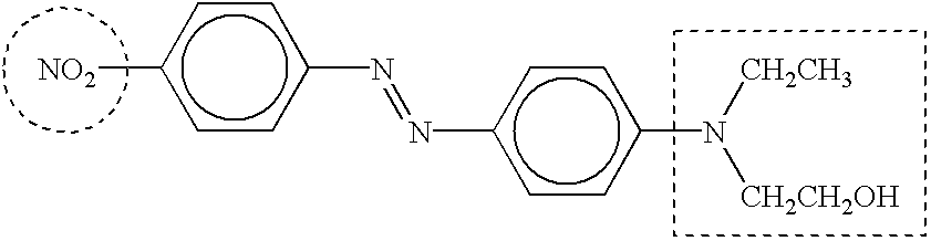
Disperse Red 1 (DR 1) 
Disperse Orange 25 (DO 25) 
Disperse Orange 1 (DO 1) 
Disperse Orange 3 (DO 3) 
TCSF 
DCV 
TCV 
styrylpyridinium cyanine dye (SPCD) 
4′-dimethylamino-N-methyl-4- stilbazolium tosylate (DAST)
Claims (28)
1. A method of making a device comprising:
forming two electrodes;
creating an electric field between the two electrodes; and
forming a waveguide between the two electrodes in the presence of the electric field.
2. The method of claim 1 , wherein the two electrodes are lithographically-defined on a substrate.
3. The method of claim 2 , wherein the waveguide comprises an organic crystal material.
4. The method of claim 3 , wherein the organic crystal material comprises an organic molecule comprising:
a doner portion, and
an acceptor portion coupled to the doner portion via a conjugated backbone.
5. An electro-optic modulator comprising:
two electrodes; and
a waveguide disposed between the two electrodes, the waveguide comprising an organic crystal.
6. The electro-optic modulator of claim 5 , wherein the organic crystal comprises:
a doner portion, and
an acceptor portion coupled to the doner portion via a conjugated backbone.
7. The electro-optic modulator of claim 6 , wherein the conjugated backbone comprises an aromatic ring.
8. The electro-optic modulator of claim 7 , wherein the aromatic ring is a benzene ring.
9. The electro-optic modulator of claim 5 , wherein the waveguide was formed in the presence of an electric field created between the two electrodes.
10. The electro-optic modulator of claim 5 , wherein the waveguide is a non-centrosymmetric organic material with substantially aligned dipole moments.
11. The electro-optic modulator of claim 10 , wherein the dipole moments were aligned using an electric field created between the two electrodes.
12. A method of making an electro-optic modulator comprising:
forming two electrodes on a substrate;
depositing a dielectric layer at least partially between the two electrodes;
creating an electric field between the two electrodes;
forming a waveguide over the dielectric layer in the presence of the electric field; and
depositing a top cladding over the waveguide.
13. The method of claim 12 further comprising:
polishing the waveguide prior to depositing the top cladding.
14. The method of claim 13 further comprising:
polishing the waveguide down to a top surface of the two electrodes.
15. The method of claim 12 , wherein forming of the waveguide further comprises:
growing a crystal by a controlled cooling of a melt.
16. The method of claim 15 , wherein the crystal comprises an organic molecule comprising a donor, an acceptor, and a conjugated backbone.
17. The method of claim 12 , wherein forming of the waveguide further comprises:
growing a crystal by controlling a rate of evaporation of a solution.
18. The method of claim 17 , wherein the crystal comprises an organic molecule comprising a donor, an acceptor, and a conjugated backbone.
19. The method of claim 12 , wherein forming of the waveguide further comprises:
aligning dipole moments of the waveguide with the electric field as the waveguide crystallizes.
20. The method of claim 12 further comprising:
applying a voltage to the two electrodes to modulate a light signal in the waveguide.
21. A method of changing a phase of an optical signal in an electro-optic modulator comprising two electrodes and an organic crystalline waveguide situated between the two electrodes, the organic crystalline waveguide having dipole moments substantially aligned in a common orientation, the method comprising:
introducing the optical signal into the organic crystalline waveguide; and
applying a voltage to the two electrodes.
22. The method of claim 21 , wherein applying the voltage to the two electrodes changes a refractive index of the organic crystalline waveguide.
23. An optical system comprising:
a laser;
an electro-optic modulator comprising two electrodes and an organic crystal waveguide between the two electrodes, the waveguide having its dipole moments substantially aligned in a common direction, the waveguide positioned to receive a light signal from the laser, the electrodes of the waveguide coupled to a signal input.
24. The optical system of claim 23 further comprising:
an amplifier to amplify a modulated light signal from the electro-optic modulator.
25. The optical system of claim 24 further comprising:
a MUX/DEMUX coupled to the electro-optic modulator.
26. The optical system of claim 25 , wherein the MUX/DEMUX is an array waveguide grating.
27. An electro-optic modulator comprising:
a splitter;
a coupler; and
a phase modulator comprising an organic crystal having its dipole moments substantially aligned in a common direction, wherein the splitter is coupled to direct a first portion of a light signal to the phase modulator and a second portion of the light signal to the coupler, and the coupler is coupled to recombine an optical signal output from the phase modulator with the second portion of the light signal.
28. The electro-optic modulator of claim 27 , wherein the splitter and the coupler are the same device.
Priority Applications (2)
| Application Number | Priority Date | Filing Date | Title |
|---|---|---|---|
| US09/991,337 US20030099420A1 (en) | 2001-11-13 | 2001-11-13 | Electro-optic modulator |
| US10/849,443 US20040213496A1 (en) | 2001-11-13 | 2004-05-18 | Electro-optic modulator |
Applications Claiming Priority (1)
| Application Number | Priority Date | Filing Date | Title |
|---|---|---|---|
| US09/991,337 US20030099420A1 (en) | 2001-11-13 | 2001-11-13 | Electro-optic modulator |
Related Child Applications (1)
| Application Number | Title | Priority Date | Filing Date |
|---|---|---|---|
| US10/849,443 Division US20040213496A1 (en) | 2001-11-13 | 2004-05-18 | Electro-optic modulator |
Publications (1)
| Publication Number | Publication Date |
|---|---|
| US20030099420A1 true US20030099420A1 (en) | 2003-05-29 |
Family
ID=25537117
Family Applications (2)
| Application Number | Title | Priority Date | Filing Date |
|---|---|---|---|
| US09/991,337 Abandoned US20030099420A1 (en) | 2001-11-13 | 2001-11-13 | Electro-optic modulator |
| US10/849,443 Abandoned US20040213496A1 (en) | 2001-11-13 | 2004-05-18 | Electro-optic modulator |
Family Applications After (1)
| Application Number | Title | Priority Date | Filing Date |
|---|---|---|---|
| US10/849,443 Abandoned US20040213496A1 (en) | 2001-11-13 | 2004-05-18 | Electro-optic modulator |
Country Status (1)
| Country | Link |
|---|---|
| US (2) | US20030099420A1 (en) |
Cited By (6)
| Publication number | Priority date | Publication date | Assignee | Title |
|---|---|---|---|---|
| US20050196101A1 (en) * | 2003-10-15 | 2005-09-08 | Hamann Hendrik F. | Method and apparatus for dynamic manipulation and dispersion in photonic crystal devices |
| US20090067796A1 (en) * | 2007-09-10 | 2009-03-12 | Fuji Xerox Co., Ltd. | Polymer optical waveguide and method for manufacturing the same |
| US20130071083A1 (en) * | 2011-09-21 | 2013-03-21 | Electronics And Telecommunications Research Institute | Optical waveguide |
| US20160054529A1 (en) * | 2013-03-25 | 2016-02-25 | Photonics Electronics Technology Research Association | Optical circuit |
| WO2023040463A1 (en) * | 2021-09-18 | 2023-03-23 | 华为技术有限公司 | Electro-optical modulator and fabrication method therefor, and optical communication system |
| WO2023183162A1 (en) * | 2022-03-25 | 2023-09-28 | Applied Materials, Inc. | Low cost fabrication of optical device using discrete grating module assembly |
Families Citing this family (1)
| Publication number | Priority date | Publication date | Assignee | Title |
|---|---|---|---|---|
| US20120114281A1 (en) * | 2009-05-04 | 2012-05-10 | University Of Delaware | System and method for free-space optical interconnections |
Citations (10)
| Publication number | Priority date | Publication date | Assignee | Title |
|---|---|---|---|---|
| US3990777A (en) * | 1974-11-05 | 1976-11-09 | Siemens Aktiengesellschaft | Non-reciprocal component element for integrated optics |
| US4717762A (en) * | 1986-09-08 | 1988-01-05 | Honeywell Inc. | Electroactive polymers having aromatic and quinonoid bonding structures |
| US5288659A (en) * | 1988-08-26 | 1994-02-22 | At&T Bell Laboratories | Photonic-integrated-circuit fabrication process |
| US5334551A (en) * | 1991-07-10 | 1994-08-02 | Nec Corporation | Method of making semiconductor optical guided-wave device |
| US5361157A (en) * | 1992-08-25 | 1994-11-01 | Nippon Hoso Kyokai | Bidirectional light transmission system and optical device therefor |
| US5406406A (en) * | 1993-04-19 | 1995-04-11 | Hoechst Aktiengesellschaft | Molecular crystal and wavelength conversion devices using the same |
| US5483609A (en) * | 1993-07-09 | 1996-01-09 | Nec Corporation | Optical device with mode absorbing films deposited on both sides of a waveguide |
| US6221565B1 (en) * | 1998-02-09 | 2001-04-24 | University Of New Mexico | Tunable bragg gratings and devices employing the same |
| US6532315B1 (en) * | 2000-10-06 | 2003-03-11 | Donald J. Lenkszus | Variable chirp optical modulator having different length electrodes |
| US6661034B2 (en) * | 2000-04-14 | 2003-12-09 | Seiko Epson Corporation | Organic light emitting device with corrugated light emitting layer |
Family Cites Families (1)
| Publication number | Priority date | Publication date | Assignee | Title |
|---|---|---|---|---|
| US5917980A (en) * | 1992-03-06 | 1999-06-29 | Fujitsu Limited | Optical circuit device, its manufacturing process and a multilayer optical circuit using said optical circuit device |
-
2001
- 2001-11-13 US US09/991,337 patent/US20030099420A1/en not_active Abandoned
-
2004
- 2004-05-18 US US10/849,443 patent/US20040213496A1/en not_active Abandoned
Patent Citations (10)
| Publication number | Priority date | Publication date | Assignee | Title |
|---|---|---|---|---|
| US3990777A (en) * | 1974-11-05 | 1976-11-09 | Siemens Aktiengesellschaft | Non-reciprocal component element for integrated optics |
| US4717762A (en) * | 1986-09-08 | 1988-01-05 | Honeywell Inc. | Electroactive polymers having aromatic and quinonoid bonding structures |
| US5288659A (en) * | 1988-08-26 | 1994-02-22 | At&T Bell Laboratories | Photonic-integrated-circuit fabrication process |
| US5334551A (en) * | 1991-07-10 | 1994-08-02 | Nec Corporation | Method of making semiconductor optical guided-wave device |
| US5361157A (en) * | 1992-08-25 | 1994-11-01 | Nippon Hoso Kyokai | Bidirectional light transmission system and optical device therefor |
| US5406406A (en) * | 1993-04-19 | 1995-04-11 | Hoechst Aktiengesellschaft | Molecular crystal and wavelength conversion devices using the same |
| US5483609A (en) * | 1993-07-09 | 1996-01-09 | Nec Corporation | Optical device with mode absorbing films deposited on both sides of a waveguide |
| US6221565B1 (en) * | 1998-02-09 | 2001-04-24 | University Of New Mexico | Tunable bragg gratings and devices employing the same |
| US6661034B2 (en) * | 2000-04-14 | 2003-12-09 | Seiko Epson Corporation | Organic light emitting device with corrugated light emitting layer |
| US6532315B1 (en) * | 2000-10-06 | 2003-03-11 | Donald J. Lenkszus | Variable chirp optical modulator having different length electrodes |
Cited By (10)
| Publication number | Priority date | Publication date | Assignee | Title |
|---|---|---|---|---|
| US20050196101A1 (en) * | 2003-10-15 | 2005-09-08 | Hamann Hendrik F. | Method and apparatus for dynamic manipulation and dispersion in photonic crystal devices |
| US8606060B2 (en) * | 2003-10-15 | 2013-12-10 | International Business Machines Corporation | Method and apparatus for dynamic manipulation and dispersion in photonic crystal devices |
| US20090067796A1 (en) * | 2007-09-10 | 2009-03-12 | Fuji Xerox Co., Ltd. | Polymer optical waveguide and method for manufacturing the same |
| US7653280B2 (en) * | 2007-09-10 | 2010-01-26 | Fuji Xerox Co., Ltd. | Polymer optical waveguide and method for manufacturing the same |
| US20130071083A1 (en) * | 2011-09-21 | 2013-03-21 | Electronics And Telecommunications Research Institute | Optical waveguide |
| US8755662B2 (en) * | 2011-09-21 | 2014-06-17 | Electronics And Telecommunications Research Institute | Optical waveguide |
| US20160054529A1 (en) * | 2013-03-25 | 2016-02-25 | Photonics Electronics Technology Research Association | Optical circuit |
| US9519115B2 (en) * | 2013-03-25 | 2016-12-13 | Photonics Electronics Technology Research Association | Optical circuit |
| WO2023040463A1 (en) * | 2021-09-18 | 2023-03-23 | 华为技术有限公司 | Electro-optical modulator and fabrication method therefor, and optical communication system |
| WO2023183162A1 (en) * | 2022-03-25 | 2023-09-28 | Applied Materials, Inc. | Low cost fabrication of optical device using discrete grating module assembly |
Also Published As
| Publication number | Publication date |
|---|---|
| US20040213496A1 (en) | 2004-10-28 |
Similar Documents
| Publication | Publication Date | Title |
|---|---|---|
| US7502530B2 (en) | Optical waveguide devices and traveling wave type optical modulators | |
| EP1714317B1 (en) | Optical devices comprising thin ferroelectric films | |
| US7693356B2 (en) | Lithium niobate optical modulator | |
| US6600843B2 (en) | Optical modulator | |
| US20040155252A1 (en) | Waveguide-bonded optoelectronic devices | |
| EP1752817A1 (en) | Optical waveguide device | |
| US6700691B2 (en) | Electro-optic modulator having high bandwidth and low drive voltage | |
| JPH03257423A (en) | Operation point trimming method of waveguide type optical modulator | |
| US5982961A (en) | Organic crystal compound optical waveguide and methods for its fabrication | |
| US4776656A (en) | TE-TM mode converter | |
| EP0709711A1 (en) | Velocity-matched electrodes for electro-optic travelling-wave modulators and method for forming the same | |
| US20030099420A1 (en) | Electro-optic modulator | |
| CN114415400A (en) | Polarization-independent electro-optic modulator based on thin-film lithium niobate and preparation method thereof | |
| JPH09211402A (en) | Broad-band light modulator | |
| JP2009222753A (en) | Optical modulator | |
| US5371812A (en) | Waveguide type optical directional coupler | |
| US6958852B2 (en) | Optical modulator, method of achieving velocity matching and impedance matching of optical modulator, and method of manufacturing optical modulator | |
| WO2021201133A1 (en) | Optical modulator | |
| CN210243999U (en) | Novel lithium niobate electro-optic modulator based on zinc oxide waveguide | |
| JPH08160368A (en) | Semiconductor light intensity modulation device and semiconductor optical device | |
| CN110646957A (en) | Novel lithium niobate electro-optical modulator based on zinc oxide waveguide and preparation method thereof | |
| US20230069468A1 (en) | Optical waveguide element and optical modulation element | |
| US20230057036A1 (en) | Optical modulation element | |
| US20230059629A1 (en) | Composite Film and Fabrication Method Therefor | |
| US20220221744A1 (en) | Integrated compact z-cut lithium niobate modulator |
Legal Events
| Date | Code | Title | Description |
|---|---|---|---|
| AS | Assignment |
Owner name: INTEL CORPORATION, CALIFORNIA Free format text: ASSIGNMENT OF ASSIGNORS INTEREST;ASSIGNORS:BHOWMIK, ACHINTYA;SKINNER, MICHAEL;REEL/FRAME:012320/0960 Effective date: 20011112 |
|
| STCB | Information on status: application discontinuation |
Free format text: ABANDONED -- FAILURE TO RESPOND TO AN OFFICE ACTION |