US12353343B2 - Semiconductor device including array of processor elements and method of controlling the same - Google Patents
Semiconductor device including array of processor elements and method of controlling the same Download PDFInfo
- Publication number
- US12353343B2 US12353343B2 US17/065,169 US202017065169A US12353343B2 US 12353343 B2 US12353343 B2 US 12353343B2 US 202017065169 A US202017065169 A US 202017065169A US 12353343 B2 US12353343 B2 US 12353343B2
- Authority
- US
- United States
- Prior art keywords
- data
- data path
- parallel computing
- unit
- units
- Prior art date
- Legal status (The legal status is an assumption and is not a legal conclusion. Google has not performed a legal analysis and makes no representation as to the accuracy of the status listed.)
- Active, expires
Links
Images


Classifications
-
- G—PHYSICS
- G06—COMPUTING OR CALCULATING; COUNTING
- G06F—ELECTRIC DIGITAL DATA PROCESSING
- G06F13/00—Interconnection of, or transfer of information or other signals between, memories, input/output devices or central processing units
- G06F13/14—Handling requests for interconnection or transfer
- G06F13/20—Handling requests for interconnection or transfer for access to input/output bus
- G06F13/28—Handling requests for interconnection or transfer for access to input/output bus using burst mode transfer, e.g. direct memory access DMA, cycle steal
-
- G—PHYSICS
- G06—COMPUTING OR CALCULATING; COUNTING
- G06F—ELECTRIC DIGITAL DATA PROCESSING
- G06F15/00—Digital computers in general; Data processing equipment in general
- G06F15/16—Combinations of two or more digital computers each having at least an arithmetic unit, a program unit and a register, e.g. for a simultaneous processing of several programs
-
- G—PHYSICS
- G06—COMPUTING OR CALCULATING; COUNTING
- G06F—ELECTRIC DIGITAL DATA PROCESSING
- G06F15/00—Digital computers in general; Data processing equipment in general
- G06F15/76—Architectures of general purpose stored program computers
- G06F15/80—Architectures of general purpose stored program computers comprising an array of processing units with common control, e.g. single instruction multiple data processors
-
- G—PHYSICS
- G06—COMPUTING OR CALCULATING; COUNTING
- G06F—ELECTRIC DIGITAL DATA PROCESSING
- G06F2213/00—Indexing scheme relating to interconnection of, or transfer of information or other signals between, memories, input/output devices or central processing units
- G06F2213/28—DMA
Definitions
- the present invention relates to a semiconductor device and its control method, for example, to a semiconductor device having a plurality of processor elements (hereinafter, also called PE) and its control method.
- PE processor elements
- DSP dynamically reconfigurable processor
- array type processor a processor having a plurality of PEs.
- the array type processor can dynamically switch operation contents carried out by the PEs and inter-PE etc. connection, and can dynamically reconfigure a configuration of the array type processor.
- Patent Document 1 discloses a technique of an array type processor, but does not disclose an array type processor superior in flexibility while it maintains high operation performance.
- a semiconductor device is as follows.
- a semiconductor device includes: a data path with a plurality of processor elements; a state transition management unit that manages a state related to a configuration of the data path; and a parallel computing unit in which an input and an output of data are sequentially executed, the output and/or input of the parallel computing unit are processed by the plural processor elements.
- the semiconductor device and its control method can be provided, the semiconductor device being capable of securing the flexibility of the processing contents while maintaining the high operation performance.
- FIG. 1 is a block diagram showing a configuration of a semiconductor device according to a first embodiment
- FIG. 2 is a block diagram showing a configuration of a parallel computing unit according to the first embodiment
- FIG. 3 A is a block diagram for explaining a state transition management unit according to the first embodiment
- FIG. 3 B is a block diagram for explaining a state transition management unit according to the first embodiment
- FIG. 4 is a block diagram showing a configuration of a PE according to the first embodiment
- FIG. 5 is a view showing an example of a configuration of a neural network
- FIG. 6 is a schematic view showing a flow of an arithmetic processing of the neural network
- FIG. 7 is a view schematically showing a matrix operation expression
- FIG. 8 is a view showing the matrix operation expression
- FIG. 9 is a block diagram showing a configuration of a parallel computing unit according to the first embodiment.
- FIG. 10 is a view showing a functional block of an arithmetic processing unit that has been realized by the array type processor according to the first embodiment
- FIG. 11 is a functional block diagram of an array type processor according to a first modification of the first embodiment
- FIG. 12 is a functional block diagram of an array type processor according to a second modification of the first embodiment
- FIG. 13 is a functional block diagram of an array type processor according to a third modification of the first embodiment
- FIG. 14 is a functional block diagram of an array type processor according to a fourth modification of the first embodiment
- FIG. 16 is a functional block diagram of an array type processor according to a sixth modification of the first embodiment
- FIG. 17 is a functional block diagram of an array type processor according to a seventh modification of the first embodiment.
- FIG. 18 is a timing diagram showing a relationship the state transition management unit according to the first embodiment and a data path;
- FIG. 19 is a block diagram showing a configuration of a semiconductor device according to a second embodiment
- FIG. 20 is a block diagram showing a configuration of a parallel computing unit according to the second embodiment
- FIG. 21 A is a view showing a relationship a local memory according to the second embodiment and the parallel computing unit;
- FIG. 21 B is a view showing a relationship a local memory according to the second embodiment and the parallel computing unit;
- FIG. 22 is a block diagram showing a configuration of a semiconductor device according to a third embodiment
- FIG. 23 is a view showing an example of a dedicated arithmetic unit according to the third embodiment:
- FIG. 24 is a plan view showing arrangement of semiconductor chips in an array type processor according to a fourth embodiment.
- FIG. 25 is a plan view showing arrangement of an array type processor according to a first modification of the fourth embodiment
- FIG. 26 is a plan view showing arrangement of an array type processor according to a second modification of the fourth embodiment.
- FIG. 27 is a plan view showing arrangement of an array type processor according to a third modification of the fourth embodiment.
- FIG. 28 is a plan view showing arrangement of an array type processor according to a fourth modification of the fourth embodiment.
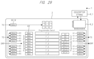
- FIG. 29 is a plan view showing arrangement of an array type processor according to a fifth modification of the fourth embodiment.
- FIG. 30 is a block diagram showing a configuration of a processing system according to a fifth embodiment.
- FIG. 31 is a block diagram showing a configuration of an array type processor according to a sixth embodiment.
- a semiconductor device suitable for a deep learning processing and its control method will be explained as an example.
- the deep learning processing is one example, and the semiconductor device and its control method that will be explained below may perform a large-scale arithmetic processing etc.
- FIG. 1 is a block diagram showing a configuration of a semiconductor device according to a first embodiment.
- the reference numeral 2 shows an array type processor mounted on a semiconductor device 1 .
- a circuit block(s) other than the array type processor 2 is also mounted on the semiconductor device 1 , but is omitted in the same figure.
- the plural arithmetic circuits 4 ( 0 _ 0 ) to 4 ( 0 _ 7 ) and 4 ( 1 _ 0 ) to 4 ( 1 _ 7 ) are not limited in particular, but are arranged along a row of the array 3 .
- the arithmetic circuits 4 ( 0 _ 0 ) to 4 ( 1 _ 7 ) may be circuits for realizing different functions or circuits for realizing the same function.
- the arithmetic circuits 4 ( 0 _ 0 ) to 4 ( 1 _ 7 ) may be multiplication circuits and/or subtraction circuits, etc.
- a plurality of data buses and a plurality of programmable switches (hereinafter, also called P-SW) are connected, in the array 3 , between the data buses and the PE 3 ( 0 _ 0 ) to 3 ( 7 _ 11 ), between the data buses and the arithmetic circuits 4 ( 0 _ 0 ) to 4 ( 0 _ 7 ), and between the data buses and the circuit block 5 .
- P-SW programmable switches
- the state transition management unit 6 manages the arithmetic circuits 4 ( 0 _ 0 ) to 4 ( 1 _ 7 ), the circuit block 5 , and the parallel computing units 7 _ 0 to 7 _ 5 .
- the state transition management unit 6 controls the on/off of the P-SW provided between each of the arithmetic circuit 4 ( 0 _ 0 ) to 4 ( 1 _ 7 ), circuit block 5 and parallel computing units 7 _ 0 to 7 _ 5 and the data bus.
- a data path is configured by the PE 3 ( 0 _ 0 ) to 3 ( 7 _ 11 ), the plural data buses, the arithmetic circuits 4 ( 0 _ 0 ) to 4 ( 1 _ 7 ), the circuit block 5 , the state transition management unit 6 , and the plural P-SW. Since the operation contents of the PE 3 ( 0 _ 0 ) to 3 ( 7 _ 11 ) and a state of the P-SW connected between the data bus and each circuit are designated by the state transition management unit 6 , a state to be concerned with a configuration of the data path will be prescribed by designation of the state transition management unit 6 . In other words, the configuration of the data path will be changed (modified) by the state transition management unit 6 changing the designation with the lapse of time.
- Each of the parallel computing units 70 to 7 _ 5 includes one input line group and one output line group. This input line group and output line group are connected to the data bus through the corresponding P-SW. Although being not limited in particular, the parallel computing units 7 _ 0 to 7 _ 5 mutually have almost the same configuration.
- each of the one parallel input line group DI( 0 ) and the one output line group DO( 0 ) of the parallel computing unit 7 _ 0 is connected to the data bus provided in the data path through the P-SW that is controlled by a switch control signal.
- FIG. 1 shows an example in which one parallel computing unit has one input line group and one output line group, but a configuration of the one parallel computing unit is not limited to this.
- one parallel computing unit may have one input line group and one output line group. This makes it possible to perform an output earlier than an input.
- i pieces of data of the output line group can be taken out from the one parallel computing unit in parallel, and the takeout of the output can be speed up at 1/i.
- the number of output line groups provided to the one parallel computing unit is two or more.
- the number of input line groups may be two or more.
- the one input line group DO( 0 ) and the one output line group DI( 0 ) shows line groups that transfer, in parallel, data of a plurality of bits to be handled (processed) as one unit.
- the number of bits to be handled as one unit is 16 bits
- the one input line group DO( 0 ) and the one output line group DI( 0 ) transfer 16-bit wide data.
- each of them can take out two pieces of 16-bit wide data from the one parallel computing unit.
- the product-sum operation unit 11 _ 0 performs a product operation between the output data from the local memory and input data from the input line group DI( 0 ), seeks an accumulation (sum operation) of operational results obtained from the product operation, and outputs it from the output terminal group.
- the remaining product-sum operation units 11 _ 1 to 11 _ n ⁇ 1 is similar, too.
- the present embodiment has explained an example in which the parallel computing unit 7 _ 0 has the n product-sum operation unit, but each of the product-sum operation units may be an operation unit capable of performing an operation of only multiplication or addition.
- the input line group DI( 0 ) and the output line group DO( 0 ) of the parallel computing unit 7 _ 0 are connected to the data path through the P-SW. Therefore, the data formed in the data path are supplied to the parallel computing unit 7 _ 0 one by one, and the product-sum operation result formed by the parallel computing unit 7 _ 0 leads to being supplied to the data path one by one.
- the register 12 is connected between the product-sum operation units 11 _ 0 to 11 _ n ⁇ 1 and the selector 13 , and the product-sum operation results are stored in the register 12 . Consequently, this makes it possible to carry out temporally and in parallel an input processing and a product-sum operation processing of data to the product-sum operation unit 11 _ 0 to 11 _ n ⁇ 1 and a processing for outputting the product-sum operation result from the parallel computing unit 7 _ 0 . In other words, a pipeline operation can be carried out. Performance of the pipeline operation makes it possible to improve efficiency of the processings.
- FIG. 2 shows a case where each of the number of inputs and the number of outputs of the parallel computing unit is one, but the present embodiment is not limited to this case.
- the number of inputs and outputs of the parallel computing unit may sufficiently be smaller than the number of product-sum operation units 11 _ 0 to 11 _ n ⁇ 1 included in the parallel computing unit 7 _ 0 .
- the number of inputs and outputs of the parallel computing unit 7 _ 0 may be two or four.
- the product-sum operation units 11 _ 0 to 11 _ n ⁇ 1 are divided into two groups of two or four units and are connected to a common input line group for each group, the number of inputs may be set to two or four.
- the parallel computing unit that uses the register 12 has been explained as an example, but the register 12 may be omitted.
- the omission of the register 12 makes it possible to achieve downsizing of the unit.
- the control unit 14 may cause the next product-sum operation to start concurrently with the output of the product-sum operation result.
- the control unit 14 repeats i times the above-mentioned processing, i.e., a series of processings of setting the initial value to the register, sequentially reading the data from the head address of the local memory 10 , and causing the product-sum operation to be performed between the input data and the local memory 10 , thereby completing the processing.
- a series of processings of setting the initial value to the register sequentially reading the data from the head address of the local memory 10 , and causing the product-sum operation to be performed between the input data and the local memory 10 , thereby completing the processing.
- sequentially reading the data from the head address of the local memory 10 has been mentioned, but the present embodiment is not limited to this.
- the next address of the predetermined address is regarded as the above-mentioned head address and the data may be read sequentially.
- control unit 14 may be configured by a data path including the PE etc. Since a configuration of the data path is defined by the state transition management unit 6 , the control signals SL_C and SL_M can be made programmable. Consequently, made programmable can be, for example, order of the data read from the local memory 10 , order of the selection by the selector 13 , and the like.
- FIG. 3 is a block diagram for explaining a state transition management unit according to the first embodiment. Here, configurations of two kinds of state transition management units will be explained.
- FIG. 3 A shows a state transition management unit having a configuration of using a memory
- FIG. 3 B shows a state transition management unit having a configuration of using a condition transition table.
- the state transition management unit 6 shown in FIG. 3 A includes a memory 6 _ 1 and a management unit 6 _ 2 . Furthermore, the management unit 6 _ 2 includes a decoder 6 _ 3 . A plurality of descriptors are stored in the memory 6 _ 1 in advance. The management unit 6 _ 2 designates an address in the memory 6 _ 1 , issues a read command, reads the descriptor from the memory 6 _ 1 , and decodes the read descriptor by a decoder 6 _ 3 . The management unit 6 _ 2 supplies, to the PE 3 ( ) and the P-SW, etc., a state signal obtained from the decoding by the decoder 6 _ 3 .
- Each of the descriptors is formed by a bit string that prescribes (defines) a state of an operation of the data path, and a state signal indicating the operation state of the data path is formed by the decoding.
- a state signal indicating the operation state of the data path is formed by the decoding.
- the management unit 6 _ 2 sequentially designates a different address in the memory 6 _ 1 , and issues a read command. Consequently, the state of the data path leads to being sequentially transitioned.
- the memory 6 _ 1 is configured by a memory that is located outside the array type processor 2 shown in FIG. 1 , but is not limited to this. For example, it may be a memory in the circuit block 5 shown in FIG. 1 or a memory provided outside the semiconductor device 1 .
- a state transition management unit 6 shown in FIG. 3 B includes a state transition table 6 _ 4 .
- the state transition table 6 _ 4 outputs designation information 6 _ 4 _ 1 for designating the operation contents of PE 3 ( ) and the state of the P-SW, and address information 6 _ 4 _ 2 for designating a next address in the state transition table 6 _ 4 .
- each of the PE 3 ( ) includes a decoder 6 _ 5 .
- the PE 3 ( 0 _ 0 ) decodes the designation information 6 _ 4 _ 1 from the state transition management unit 6 by the decoder 6 _ 5 .
- the PE 3 ( 0 _ 0 ) determines operation contents of its own and a state of the corresponding P-SW.
- the designation information 6 _ 4 _ 1 is a bit string for prescribing the operation contents of PE 3 ( ) and the state of the P-SW.
- the parallel computing units 7 _ 0 to 7 _ 5 have the product-sum operation units 110 to 11 _ n ⁇ 1, and obtain the results of the product-sum operations by inputting a large number of data.
- the results of the product-sum operations are taken out one by one by the selector 13 . It appears that a large number of cycles is required for the input and output of the data in order to take out it one by one. It is desired in those cycles to fix the configuration of the data path without changing it.
- the state transition management unit 6 it is usually desired for the state transition management unit 6 to work (run) so as to sometimes change configuration of the data path without changing the configuration of the data path.
- a period of using the parallel computing units 7 _ 0 to 7 _ 5 is regarded as a normal period, and the state transition management unit 6 works so as to maintain the configuration of the data path.
- the state transition management unit 6 works so as to change the configuration of the data path.
- the data path and the state transition management unit 6 are configured so as to increase an operation frequency, for example, so as to shorten the configuration of the data path in the period in which the configuration of the data path is fixed.
- the data is inputted by multiplying a multi-cycle and the data is outputted by multiplying a multi-cycle.
- the state of the data path is transitioned at one cycle or changed in one cycle, efficiency decreases very much. Therefore, for example, the transition of the state and the change of the configuration of the data path are carried out by multiplying the multi-cycle, and it is desired to achieve the downsizing of the circuit scale and the speedup of the operation frequency. This will be explained by using, as an example, a case of utilizing the state transition management unit 6 shown in FIG. 3 A .
- Recited as the descriptor divided per function are a descriptor for designating a transfer of an initial value to the memory included in the circuit block 5 , a descriptor for designating a path of input data that uses a DMAC included in the circuit block 5 , a descriptor for designating an operation that uses the PE, a descriptor for designating a path of output data that uses the DMAC included in the circuit block 5 , and the like, if being exemplified with reference to FIG. 1 .
- FIG. 4 is a block diagram showing the configuration of the PE according to the first embodiment.
- the PE 3 ( 1 _ 1 ) shown in FIG. 1 will be explained as a representative.
- the element b 0 is inputted into the product-sum operation units 11 _ 0 to 11 _ n ⁇ 1 at the same time; a product operation unit MX 1 in each of the product-sum operation units 11 _ 0 to 11 _ n ⁇ 1 carries out the product operation between the element from the corresponding local memory 10 and the element b 0 ; and an adder AD 1 performs addition of the product operation result and the bias value C and stores it in the register RG 1 .
- an operation of a part which is surrounded with a solid line leads to being carried out.
- the state transition management unit 6 It is desired to maintain the state transition management unit 6 so as not to change the configuration of the data path while the respective processings of the product-sum operation, BatchNorm, and the activation are performed, namely, while a series of processings shown in FIG. 10 is completed.
- the state transition management unit 6 instructs the PE etc. so that the next configuration of the data path becomes the next configuration at once or after a lapse of hours of several cycles.
- a first modification shows an arithmetic processing unit that can perform a plurality of different operations with respect to the same input data DI.
- a case that the number of processings performed in parallel lacks is thought about. Thought about as a specific example is a case where the number of product-sum operation units 11 included in the parallel computing unit 7 lacks with respect to the number of weights performed in parallel to the same input data DI. In other words, as mentioned with reference to FIG. 8 , there is a case where the number of columns of the matrix W exceeds the number of product-sum operation units included in one parallel computing unit 7 .
- the parallel computing unit 7 commonly uses one piece of input data DI with the plural product-sums operation units 11 , and carries out the processing(s).
- the weights are divided and store into each local memory 10 of the plural parallel computing units.
- the weight is 40 (a 0 , 0 to a 0 , 39 in FIG. 8 )
- these 40 weights are divided in 20 weights, and are stored in the local memories 10 of the parallel computing units 7 _ 0 , 7 _ 1 .
- the output data outputted from each parallel computing unit is different for each parallel computing unit, and so are outputted individually.
- the state transition management unit 6 gives such instructions that the BatchNorm function part 42 _ 1 , 42 _ 2 and the activation function part 43 _ 1 , 43 _ 2 are configured by the plural PEs arranged on the array 3 .
- the state transition management unit 6 gives instructions to the parallel computing units 7 _ 0 , 7 _ 1 as a parallel computing unit, and gives instructions to the DMAC included in circuit block 5 for the DMAC 41 , 44 _ 1 , 44 _ 2 as a DMAC.
- the input data DI is transferred to the parallel computing units 7 _ 0 , 7 _ 1 by the DMAC 41 from the external memory 30 .
- Each of the parallel computing units 7 _ 0 , 7 _ 1 carries out the product-sum operation for the same input data DI.
- the data stored in the local memory 10 of the parallel computing unit 70 is different from the data stored in the local memory 10 of the parallel computing unit 7 _ 1 .
- the processings of BatchNorm and activation are performed by the BatchNorm function part 42 _ 1 and the activation function part 43 _ 1 , and the result is transferred as output data DO_ 1 to the external memory 30 by the DMAC 44 _ 1 .
- the processings of BatchNorm and activation are performed by the BatchNorm function part 422 and the activation function part 43 _ 2 , and the result is transferred as output data DO_ 2 to the external memory 30 by the DMAC 44 _ 2 .
- the processing results formed in parallel are serialized and can be transferred to the external memory 30 .
- the output of one parallel computing unit is transferred as one piece of sequential data, it can be transferred as one piece of sequential data to the external memory 30 even when a division processing is performed by the plural parallel computing unit.
- FIG. 13 is a function block diagram showing a third modification of the arithmetic processing unit realized by the array type processor according to the first embodiment. As FIG. 13 is similar to FIG. 12 , a difference therebetween will be mainly explained.
- the respective processing results of the parallel computing unit 7 _ 0 , 7 _ 1 are added by an addition function part 46 .
- the processings of the BatchNorm and the activation are performed to a result obtained by this addition through the BatchNorm function part 42 and the activation function part 43 , and the result is transferred as output data DO_ 2 to the external memory 30 by the DMAC 44 .
- the addition function part 46 is configurated by combining the predetermined PE and the P-SW corresponding to it.
- the third modification is suitable to a case where the number of pieces of input data is heavy.
- the arithmetic processing unit 40 is suitable to a case where the row number m of the matrix In is high.
- the input data read from the matrix In is divided into input data DI_ 1 , DI_ 2 .
- the product-sum operations are carried out by the parallel arithmetic units 7 _ 0 , 7 _ 1 , and add the product-sum operation results are added by the addition function part 46 .
- the processings of BatchNorm and activation is performed by the DMAC 44 , and the addition result performed is transferred to the external memory 30 .
- the processing of the product-sum operation is performed and the processings of BatchNorm and activation etc. can be also performed.
- the delay function part 47 is realized by, for example, setting as a delay buffer or FIFO the memory provided in the circuit block 5 .
- the delay buffer or FIFO is provided in the circuit block 5 in advance, and this may be used.
- the fourth modification is suitable to use the same input data with time lag.
- the input data DI is transferred to the parallel computing unit 7 _ 0 by the DMAC 41 and is transferred to the delay function part 47 .
- the input data DI transferred to the delay function part 47 is maintained by the delay function part 47 , and the maintained input data DI delays and is supplied to the parallel computing unit 7 _ 1 .
- the output data DO_ 1 corresponding to the input data DI is transferred to the external memory 30 and the output data DO_ 2 corresponding to the same input data DI delays and is transferred to the external memory 30 . In this way, it is not necessary to transfer the same input data DI from the external memory 30 twice.
- FIG. 15 is a function block diagram showing a fifth modification of the arithmetic processing unit realized by the array type processor according to the first embodiment. As FIG. 15 is similar to FIG. 11 , a difference therebetween will be mainly explained.
- each of the parallel computing units 7 ′_ 0 , 7 ′_ 1 has a configuration in which the local memory 10 is removed from the parallel computing unit 7 shown in FIG. 2 .
- the local memory 10 ′_ 1 , 10 ′_ 2 function as local memories of the parallel computing units 7 ′_ 0 , 7 ′_ 1 .
- the parallel computing units 7 ′_ 0 , 7 ′_ 1 carry out the product-sum operations by using the data from the local memories 10 ′_ 1 , 10 ′_ 2 .
- FIG. 16 is a function block diagram showing a sixth modification of the arithmetic processing unit realized by the array type processor according to the first embodiment. As FIG. 16 is similar to FIG. 15 , a difference therebetween will be mainly explained.
- the difference is that the local memory 10 ′ common to two parallel computing units 7 ′_ 0 , 7 ′_ 1 is located.
- the sixth modification is suitable to a case where the product-sum operation of the same data is performed with respect to the input data DI_ 1 , DI_ 2 mutually different.
- the common data is supplied to the parallel computing units 7 ′_ 0 , 7 ′_ 1 . Since the input data supplied to the parallel computing units 7 ′_ 0 , 7 ′_ 1 is different from the input data DI_ 1 , DI_ 2 , the parallel computing units 7 ′ _ 0 , 7 ′_ 1 perform the product-sum operation to the different input data by using the same data from the local memory 10 ′.
- FIG. 20 is a block diagram showing a configuration of the parallel computing unit according to the second embodiment.
- the reference numeral 7 ′_ 0 shows a parallel computing unit.
- the configuration of the parallel computing unit 7 ′_ 0 is similar to the parallel computing unit 70 shown in FIG. 2 .
- the parallel computing unit 7 ′_ 0 includes no local memory and the other input terminal groups of the product-sum operation units 11 _ 0 to 11 _ n ⁇ 1 are connected to the data bus 50 .
- connected to the one input terminal groups of the product-sum operation units 11 _ 0 to 11 _ n ⁇ 1 is the input line group DI( 0 ) similarly to the parallel computing unit 7 _ 0 .
- the input data supplied to the parallel computing unit is one parallel such as a 16-bit width and it is narrower than the above-mentioned wirings, so that it is desired that the flexibility of the wirings is ensured on an input line group DI( 0 ) side.
- FIG. 21 is view showing a relationship between the local memory and the parallel computing unit according to the second embodiment.
- FIG. 21 A shows a case of making a local memory and a parallel computing unit one to one
- FIG. 21 B shows a case of assigning three local memories to a parallel computing unit.
- the number of local memories to be assigned to the parallel computing unit is not limited to three, and may be two or be four or more.
- FIG. 21 exemplifies a case of providing nine local memories 10 ′_ 0 to 10 ′_ 8 and nine parallel computing unit 7 ′_ 0 to 7 ′_ 8 .
- the local memories 10 ′_ 0 to 10 ′_ 8 are assigned so as to correspond to the parallel computing units 7 ′_ 0 to 7 ′_ 8 one to one.
- the parallel computing unit 7 ′ _ 0 is assigned to the local memory 10 ′_ 0 one-on-one. In this way, the parallel computing unit 7 ′_ 0 can use only the corresponding one local memory 10 ′_ 0 .
- the local memory 10 ′_ 0 is equal to the local memory 10 in the parallel computing unit of FIG. 2 .
- three local memories are collected to be one and are assigned to three parallel computing unit.
- the local memories 10 ′_ 0 to 10 ′_ 2 are collected to be one and are assigned to three parallel computing units 7 ′_ 0 to 7 ′_ 2 .
- a selector 510 is connected between one bundle of local memories and the corresponding parallel computing units 7 ′_ 0 to 7 ′_ 2 .
- the selector 51 _ 0 any one of the parallel computing units 7 ′_ 0 to 7 ′_ 2 is connected to the local memories 10 ′_ 0 to 10 ′_ 2 . This makes it possible to read the data stored in three local memories by any one of three parallel computing units 7 ′_ 0 to 7 ′_ 2 .
- each of the three parallel computing units can use the triple memory capacity of the local memory.
- the memory capacity viewed from the parallel computing units can be increased.
- the local memories 10 ′_ 0 to 10 ′_ 2 has been explained as an example, but other local memories are similar, too.
- Each of the selectors 51 _ 0 to 51 _ 2 works so as to select or unselect in parallel the data of the number of bits equivalent to the number of product-sum operation units that configures the corresponding parallel computing unit.
- a bit width to be processed in parallel is very large in each of the selectors 51 _ 0 to 51 _ 2 . Therefore, it is desired that the selectors 51 _ 0 to 51 _ 2 are configured by dedicated (exclusive) hardware.
- the selector may be configured by a PE 3 ( ) or/and P-SW.
- the selectors 51 _ 0 to 51 _ 2 are controlled by the state transition management unit 6 . In this way, for example, as showed in FIG. 21 A , the present embodiment is programmed so that the local memory and the parallel computing unit become one-on-one and the parallel computing unit is connected to the local memory through the selector.
- FIG. 19 shown has been an example in which the state transition management unit 6 controls the product-sum operation units 11 _ 0 to 11 _ n ⁇ 1, the register 12 , the selector 13 , and the selectors 510 to 51 _ 2 , and selects the data supplied to the parallel computing units 7 ′_ 0 to 7 ′_ 5 among the data from the local memories 10 ′_ 0 to 10 ′_ 5 .
- the present embodiment is not limited to this.
- the present embodiment may have such a configuration as to provide the control unit in the parallel computing unit 7 ′ and control the product-sum operation units 11 _ 0 to 11 _ n ⁇ 1, the register 12 , the selector 13 , and the selectors 51 _ 0 t 51 _ 2 .
- FIG. 19 shown has been an example in which the local memory 10 ′_to 10 ′_ 5 and the parallel computing unit 7 ′_ 0 to 7 ′_ 5 are connected to one data bus 50 , but the present embodiment is not limited to this.
- the data bus 50 may be divided into a plurality of data buses.
- the data bus 50 may be divided into three data buses, and three local memories and three parallel computing units may be connected to each of the divided data buses.
- the local memories 10 ′_ 0 to 10 ′_ 2 and the parallel computing units 7 ′_ 0 to 7 ′_ 2 are connected to the first divided data bus; the local memories 10 ′_ 3 to 10 ′_ 5 and the parallel computing unit 7 ′_ 3 to 7 ′ 5 are connected to the second divided data bus; and the local memories 10 ′_ 6 to 10 ′_ 8 and the parallel computing units 7 ′_ 6 to 7 ′ 8 are connected to the third divided data bus.
- the selector is structurally provided to each of the divided data buses, the configuration shown in FIG. 21 B can be easily realized.
- Controlling the selectors 51 _ 0 to 51 _ 2 by the state transition management unit 6 make it possible to dynamically change the connection between the local memories 10 ′_ 0 to 10 ′_ 8 and the parallel computing units 7 ′_ 0 to 7 ′_ 8 depending on situations of an application and a layer to be carried out. For example, by a lapse of time, it is possible to dynamically change from a state of the connection shown in FIG. 21 B to a state of the connection shown in FIG. 21 A .
- FIG. 22 is a block diagram showing a configuration of a semiconductor device according to a third embodiment. Since FIG. 22 is similar to FIG. 1 , a difference therebetween will be mainly explained.
- the dedicated arithmetic unit 52 shows a dedicated arithmetic unit that performs the operation of the BatchNorm processing
- dedicated arithmetic unit 53 shows a dedicated arithmetic unit that performs the operation the activation processing.
- shown is an example in which two dedicated arithmetic units are arranged in the array.
- the number of dedicated arithmetic units and their placement are not limited to this.
- FIG. 23 is a view showing an example of a dedicated arithmetic unit according to the third embodiment.
- the reference numeral 54 shows a dedicated arithmetic unit that perform an operation about the pooling.
- the dedicated arithmetic unit 54 performs the operation about the pooling processing with respect to the input data Din, and outputs 16-bit wide data.
- Reference numeral 58 shows a dedicated arithmetic unit that performs a processing about the padding, inputs 16-bit wide data, performs the operation, and outputs the 16-bit wide data. In a case of, for example, no padding, the dedicated arithmetic unit 58 performs a processing of inserting a value of 0 into the data regularly.
- the dedicated arithmetic unit 52 that performs the operation about the BatchNorm processing carries out an operation with respect to a parameter and a 16-bit wide input Din, and outputs 16-bit wide data Dout. Furthermore, the dedicated arithmetic unit 53 that performs the operation about the activation processing inputs 16-bit wide data, and outputs the 16-bit wide data.
- the DMAC which performs data transmission with, for example, the external memory 30 ( FIG. 6 ) can be also arranged as the dedicated arithmetic units 55 , 56 in the array 3 .
- the delay function part 47 explained in FIG. 14 etc. can be also placed as the dedicated arithmetic unit 57 in the array 3 .
- the parallel computing unit 59 can be placed as one dedicated arithmetic unit in the array 3 .
- the arithmetic unit is not limited to the dedicated arithmetic unit exemplified in FIG. 22 , and can be placed as a dedicated arithmetic unit in the array 3 and made an element of the data path as long as performing an operation of inputting and outputting the small number of pieces of data.
- Use of the dedicated arithmetic unit makes it possible to perform the processing more effectively than realization of the arithmetic unit by the combination of the general arithmetic units and to be arranged effectively.
- the dedicated arithmetic unit is usable only for its purpose, an arithmetic unit that, as targets, corresponds to a processing with high occurrence frequency or that has high effects in speed and occupation area by being dedicated is desirable made a dedicated arithmetic unit.
- the dedicated arithmetic unit as a target other than the above-mentioned target can be desirably realized by a combination of the PEs etc.
- the dedicated arithmetic unit arranged in the array 3 is connected to a data bus through the P-SW similarly to the PE 3 ( 1 _ 1 ) shown in FIG. 4 .
- This state of the P-SW is controlled by the state transition management unit 6 . This makes it possible to use any dedicated arithmetic unit.
- FIG. 24 is a plan view showing arrangement of semiconductor chips in an array type processor according to a fourth embodiment.
- FIG. 24 shows arrangement suitable to a case where the operation performance of the parallel computing unit decides performance of an application as a target of the processing carried out by the array type processor 2 .
- each of the reference numerals 7 _ 0 to 7 _ 8 show parallel computing units as explained in FIGS. 1 and 2 , etc.
- the parallel computing units 7 _ 0 to 7 _ 11 are arranged into array form in FIG. 24 in the vicinity of a central part of the array type processor 2 so as to be close to a mutual space (gap) between the parallel computing units.
- the reference numerals 60 , 61 show DMACs
- the reference numeral 62 shows a memory
- the reference numerals 3 ( 0 _ 0 ) to 3 ( 0 _ 7 ) shows PEs.
- a programmable switch shows a switch group for connecting each of the DMACs 60 , 61 , memory 62 , parallel computing unit 7 , and PE 3 ( ) to the data bus.
- these switch groups are the above-mentioned group of P-SWs.
- the memory 6 _ 1 configuring the state transition management unit 6 is placed outside the array type processor 2 and the management unit 6 _ 2 is arranged inside the array type processor 2 although both are not limited in particular.
- the array type processor 2 is connected to an external memory such as the external memory 30 ( FIG. 6 ) through the data bus 70 .
- the DMACs 60 , 61 and memory 62 shown in FIG. 24 are provided to the circuit block 5 shown in FIG. 1 .
- the DMAC denoted by the reference numeral 60 _W among the DMACs 60 is a DMAC that transfers the data to local memories 10 ( FIG. 2 ) of the parallel computing units 7 _ 0 to 7 _ 8 from the data bus 70 . Since the data stored in the local memory 10 is weight data in the deep learning processing, the DMAC 60 _W leads to transferring the weight data.
- the DMAC 60 transfers, to the array type processor 2 , the input data supplied from the external memory 30 through the data bus 70 , and the DMAC 61 transfers a processing result(s) of the array type processor 2 to the external memory 30 through the data bus 70 .
- a descriptor string that is configured by the plural descriptors is stored in the memory 6 _ 1 , and is read to the management unit 6 _ 2 sequentially.
- the management unit 6 _ 2 outputs a state signal according to the read descriptor.
- the configuration of the data path is prescribed, and the processing is performed to the input data that is obtained from the external memory 30 supplied to the array type processor 2 , and its processing result is supplied to the external memory 30 .
- the PE 3 ( ) and the memory 62 are arranged closer to the array of the parallel computing unit than the DMACs 61 , 60 .
- FIG. 24 shown has been an example of collecting the important parallel computing units and arranging them into array form in order to shorten a mutual distance. However, it is desired to set each arrangement in consideration of importance of the connection relation, and areas and the number, etc. of respective elements also regarding other elements such as PEs.
- the plural PEs 3 ( ) are arranged in the array 3 . However, in the array 3 , only the PEs 3 ( ) are not arranged collectively and the PEs are arranged so as to sandwich the arithmetic circuit 4 ( 0 _ 0 ) to 4 ( 1 _ 3 ), dedicated arithmetic units 52 , 53 between the PEs 3 ( ).
- each distance between the PEs 3 ( ) and the arithmetic circuits 4 ( 0 _ 0 ) to 4 ( 1 _ 3 ) and dedicated arithmetic units 52 , 53 is suppressed so as not to be far.
- FIG. 25 is a plan view showing arrangement of an array type processor according to a first modification of the fourth embodiment. Since FIG. 25 is similar to FIG. 24 , a difference therebetween will be mainly explained.
- the difference is to reduce the number of PEs 3 ( ) having the general arithmetic units and increase the number of dedicated operation units in order to improve processing efficiency of processing parts other than the parallel computing unit 7 .
- the dedicated arithmetic units 52 , 53 shown in FIG. 23 are added to the array type processor 2 , and the number of PEs is reduced up to 3 ( 0 _ 0 ) to 3 ( 0 _ 4 ). In this way, the contents capable of being handled by the array type processor 2 have been specialized, and the processing efficiency of the suitable application can be improved.
- the parallel computing unit is not arranged into array form but is arranged into line form in the vicinity of the central part of the array type processor 2 .
- the number of parallel computing units becomes less than that shown in FIG. 25 .
- This arrangement is suitable to a case where the number of parallel computing units is relatively little.
- this arrangement is suitable to a case where a large number of signals are sent and received between the adjacent parallel computing units.
- basic of the parallel computing unit is to have few data input and output, but parallel data inside each parallel computing unit can be transferred as a number of signals mentioned above at the same time only between the adjacent parallel computing units.
- FIG. 26 another array type processor DRP provided outside the array type processor 2 is connected to a bus in the data path through a programmable switch.
- the dedicated arithmetic unit is increased in number and the PE 3 ( ) is reduced in number. Therefore, it is thought that the processing uncapable of being realized or the processing bringing low performance by the dedicated arithmetic unit occurs.
- the processing uncapable of being realized or the processing bringing low performance by the dedicated arithmetic unit is implemented by the array type processor DRP provided outside.
- the result handled by the array type processor DRP is supplied to the data bus in the data path through the programmable switch.
- the data is supplied from the data bus in the data path to the array type processor DRP through the programmable switch in order to let the array type processor DRP perform the processing.
- the sending and receiving of the data are carried out between the array type processor DRP and the array type processor 2 without using the DMACs 60 , 61 . This makes it possible to achieve the improvement of the processing speed.
- an input side FIFO and an output side FIFO may be provided to the array type processor.
- the data from the array type processor DRP is inputted into the input side FIFO, and are transferred to the data bus in the data path from the input side FIFO.
- the data from the data bus in the data path is transferred to the output side FIFO, and is supplied to the external memory 30 from the output side FIFO.
- the array type processors explained in the first and third embodiments are used as the array type processor 2 .
- the local memory 10 , product-sum operation units 11 _ 0 to 11 _ n ⁇ 1, and DMACs 41 , 44 among the circuit blocks included in the array type processor 2 are illustrated in FIG. 30 in order to avoid the drawing being complicated.
- the local memory 10 and the product-sum operation units 11 _ 0 to 11 _ n ⁇ 1 shown in FIG. 30 correspond to the local memory and the product-sum operation units included in the parallel computing unit 7 _ 0 shown in FIG. 2 .
- the DMAC 41 functions to transfer the input data to the parallel computing unit
- the DMAC 44 functions to transfer the output data.
- the array type processor 2 includes the dedicated operation unit explained in FIG. 22 .
- the external memory 30 includes a first memory area 30 _ 1 for storing the input data DI, and a second memory area 30 _ 2 for storing the output data DO of the handled result.
- the output data DO is formed by carrying out a predetermined processing with respect to the input data DI.
- this determined processing is distributed (dispersed) by the array type processors 2 , DRP.
- the predetermined processing is carried out by combining the array type processors 2 , DRP.
- the array type processor 2 is configured so as to include the parallel computing unit 7 , the dedicated operation unit, and the necessary minimum PEs 3 ( ) in order to make the processing efficiency of the basic processing among the predetermined processings good.
- the processing not to be performed by the array type processor 2 among the predetermined processings make the array type processor DRP carried out.
- the DMAC 41 transfers the input data DI in array type processor 2 , and processing for the input data DI into the array type processor 2 , and the processing to the input data DI is carried out inside the array type processor 2 . Its result is supplied as data 86 to the selector 81 by the DMAC 44 , and is stored in the second memory area 30 _ 2 through the selector 81 .
- the input data DI is supplied to the array type processor DRP.
- the array type processor DRP for example, a preprocessing is carried out with respect to the supplied input data, and the data 84 formed by the preprocessing is transferred in the array type processor 2 by the DMAC 41 , and is processed in the array type processor 2 .
- the handled data 85 is transferred to the array type processor DRP by the DMAC 44 , and the array type processor DRP performs the post-processing to the data 85 and stores its result in the memory area 30 _ 2 as the output data DO through the selector 81 as the data 83 .
- the array type processor DRP performs the processing to the data 82 , outputs its result to the selector 81 as the data 83 , and stores it in the second memory area 302 as the output data DO from the selector 81 .
- the processing may be performed by transferring, to the first memory area 30 _ 1 , the output data stored in the second memory area 30 _ 2 and suppling as input data DI it to the array type processor 2 again.
- a plurality of processings are carried out in one array type processor.
- the first state transition management unit 6 A controls the divided data path corresponding to the parallel computing units 7 _ 0 , 7 _ 1 and the array OP 1 ;
- the second state transition management unit 6 B controls the divided data path corresponding to the parallel computing units 7 _ 2 , 7 _ 3 and the array OP 2 ;
- the third state transition management unit 6 C controls the divided data path corresponding to the parallel computing units 7 _ 4 , 7 _ 5 and the array OP 3 .
- the first state transition management unit 6 A controls the parallel computing units 7 _ 0 , 7 _ 1 so as to perform a processing such as activation of the first layer shown in FIG. 5 and a processing of a product-sum operation before the first layer by the corresponding parallel computing units 7 _ 0 , 7 _ 1 and array OP 1 , and prescribes a configuration of the divided data path corresponding to the array OP 1 .
- the second state transition management unit 6 B controls the parallel computing units 7 _ 2 , 7 _ 3 so as to perform a processing such as activation of the second layer shown in FIG.
- the third transition management unit 6 C controls the parallel computing units 7 _ 4 , 7 _ 5 so as to perform a processing such as activation of the output layer shown in FIG. 5 and a processing of a product-sum operation before the output layer by the corresponding parallel computing units 7 _ 4 , 7 _ 5 and array OP 3 , and prescribes a configuration of the divided data path corresponding to the array OP 3 .
- the DMAC 44 transfers, as the output data DO, the data DI 2 to the external memory 30 .
- the processing of the second layer and the processing of the product-sum operation before it lead to being performed to the data inputted at the next timing in the parallel computing units 7 _ 2 , 7 _ 3 and array OP 2 corresponding to the second state transition management unit 6 B.
- the plural processings related to the different layers are performed so as to overlap temporally. Therefore, the reduction in processing time can be achieved.
Landscapes
- Engineering & Computer Science (AREA)
- Theoretical Computer Science (AREA)
- Physics & Mathematics (AREA)
- General Engineering & Computer Science (AREA)
- General Physics & Mathematics (AREA)
- Computer Hardware Design (AREA)
- Software Systems (AREA)
- Computing Systems (AREA)
- Multi Processors (AREA)
- Advance Control (AREA)
- Image Processing (AREA)
Abstract
Description
-
- [Patent Document 1] Japanese Unexamined Patent Application Publication No. 2001-312481).
Claims (9)
Applications Claiming Priority (2)
| Application Number | Priority Date | Filing Date | Title |
|---|---|---|---|
| JP2019-189601 | 2019-10-16 | ||
| JP2019189601A JP7346235B2 (en) | 2019-10-16 | 2019-10-16 | semiconductor equipment |
Publications (2)
| Publication Number | Publication Date |
|---|---|
| US20210117352A1 US20210117352A1 (en) | 2021-04-22 |
| US12353343B2 true US12353343B2 (en) | 2025-07-08 |
Family
ID=75402787
Family Applications (1)
| Application Number | Title | Priority Date | Filing Date |
|---|---|---|---|
| US17/065,169 Active 2040-10-11 US12353343B2 (en) | 2019-10-16 | 2020-10-07 | Semiconductor device including array of processor elements and method of controlling the same |
Country Status (3)
| Country | Link |
|---|---|
| US (1) | US12353343B2 (en) |
| JP (1) | JP7346235B2 (en) |
| CN (1) | CN112667559A (en) |
Families Citing this family (1)
| Publication number | Priority date | Publication date | Assignee | Title |
|---|---|---|---|---|
| US20220398441A1 (en) * | 2021-06-11 | 2022-12-15 | Renesas Electronics Corporation | Semiconductor device |
Citations (19)
| Publication number | Priority date | Publication date | Assignee | Title |
|---|---|---|---|---|
| JPH08185389A (en) | 1994-05-10 | 1996-07-16 | Matsushita Electric Ind Co Ltd | Orthogonal transform processor |
| US5596518A (en) | 1994-05-10 | 1997-01-21 | Matsushita Electric Industrial Co., Ltd. | Orthogonal transform processor |
| US20010018733A1 (en) | 2000-02-25 | 2001-08-30 | Taro Fujii | Array-type processor |
| US20030126404A1 (en) | 2001-12-26 | 2003-07-03 | Nec Corporation | Data processing system, array-type processor, data processor, and information storage medium |
| US20040078093A1 (en) | 2002-10-11 | 2004-04-22 | Nec Electronics Corporation | Array-type processor |
| US20050050233A1 (en) | 2003-08-28 | 2005-03-03 | Nec Electronics Corporation | Parallel processing apparatus |
| JP2012226578A (en) | 2011-04-20 | 2012-11-15 | Renesas Electronics Corp | Delay analysis method for semiconductor integrated circuit, delay analysis program, and delay analysis device |
| US8327187B1 (en) * | 2009-09-21 | 2012-12-04 | Tilera Corporation | Low-overhead operating systems |
| US8359462B1 (en) * | 2007-11-21 | 2013-01-22 | Marvell International Ltd. | Method and apparatus for programmable coupling between CPU and co-processor |
| US8447957B1 (en) * | 2006-11-14 | 2013-05-21 | Xilinx, Inc. | Coprocessor interface architecture and methods of operating the same |
| US20190042923A1 (en) * | 2017-08-07 | 2019-02-07 | Intel Corporation | System and method for an optimized winograd convolution accelerator |
| US20190079801A1 (en) * | 2017-09-14 | 2019-03-14 | Electronics And Telecommunications Research Institute | Neural network accelerator including bidirectional processing element array |
| US20190236049A1 (en) * | 2018-01-31 | 2019-08-01 | Amazon Technologies, Inc. | Performing concurrent operations in a processing element |
| US20190294413A1 (en) * | 2018-03-23 | 2019-09-26 | Amazon Technologies, Inc. | Accelerated quantized multiply-and-add operations |
| US20200073470A1 (en) * | 2018-08-31 | 2020-03-05 | Qualcomm Incorporated | Systems and methods for controlling instantaneous current changes in parallel processors |
| US20200089506A1 (en) * | 2017-05-19 | 2020-03-19 | Movidius Ltd. | Methods, systems and apparatus to improve convolution efficiency |
| US10678479B1 (en) * | 2018-11-29 | 2020-06-09 | Amazon Technologies, Inc. | Registers for restricted memory |
| US20210011288A1 (en) * | 2019-07-09 | 2021-01-14 | Facebook Technologies, Llc | Systems and methods for distributing a neural network across multiple computing devices |
| US20210157548A1 (en) * | 2019-11-27 | 2021-05-27 | Amazon Technologies, Inc. | Systolic array including fused multiply accumulate with efficient prenormalization and extended dynamic range |
Family Cites Families (7)
| Publication number | Priority date | Publication date | Assignee | Title |
|---|---|---|---|---|
| JP4594666B2 (en) | 2004-07-12 | 2010-12-08 | 富士通株式会社 | Reconfigurable computing device |
| JP2006202271A (en) | 2004-12-22 | 2006-08-03 | Nec Electronics Corp | Stream processor and information processor |
| JP5431003B2 (en) | 2009-04-03 | 2014-03-05 | スパンション エルエルシー | Reconfigurable circuit and reconfigurable circuit system |
| JP2017027212A (en) | 2015-07-17 | 2017-02-02 | 富士ゼロックス株式会社 | Data processing device |
| CA3108151C (en) | 2017-02-23 | 2024-02-20 | Cerebras Systems Inc. | Accelerated deep learning |
| US11409692B2 (en) * | 2017-07-24 | 2022-08-09 | Tesla, Inc. | Vector computational unit |
| US20200210818A1 (en) | 2017-11-02 | 2020-07-02 | Tdk Corporation | Array device including neuromorphic element and neural network system |
-
2019
- 2019-10-16 JP JP2019189601A patent/JP7346235B2/en active Active
-
2020
- 2020-10-07 US US17/065,169 patent/US12353343B2/en active Active
- 2020-10-15 CN CN202011102904.7A patent/CN112667559A/en active Pending
Patent Citations (23)
| Publication number | Priority date | Publication date | Assignee | Title |
|---|---|---|---|---|
| JPH08185389A (en) | 1994-05-10 | 1996-07-16 | Matsushita Electric Ind Co Ltd | Orthogonal transform processor |
| US5596518A (en) | 1994-05-10 | 1997-01-21 | Matsushita Electric Industrial Co., Ltd. | Orthogonal transform processor |
| US20010018733A1 (en) | 2000-02-25 | 2001-08-30 | Taro Fujii | Array-type processor |
| JP2001312481A (en) | 2000-02-25 | 2001-11-09 | Nec Corp | Array type processor |
| US20030126404A1 (en) | 2001-12-26 | 2003-07-03 | Nec Corporation | Data processing system, array-type processor, data processor, and information storage medium |
| JP2003196246A (en) | 2001-12-26 | 2003-07-11 | Nec Corp | Data processing system, array type processor, data processor, computer program and information storage medium |
| US20040078093A1 (en) | 2002-10-11 | 2004-04-22 | Nec Electronics Corporation | Array-type processor |
| JP2004133780A (en) | 2002-10-11 | 2004-04-30 | Nec Electronics Corp | Array processor |
| US20050050233A1 (en) | 2003-08-28 | 2005-03-03 | Nec Electronics Corporation | Parallel processing apparatus |
| JP2005078177A (en) | 2003-08-28 | 2005-03-24 | Nec Electronics Corp | Parallel-arithmetic unit |
| US8447957B1 (en) * | 2006-11-14 | 2013-05-21 | Xilinx, Inc. | Coprocessor interface architecture and methods of operating the same |
| US8359462B1 (en) * | 2007-11-21 | 2013-01-22 | Marvell International Ltd. | Method and apparatus for programmable coupling between CPU and co-processor |
| US8327187B1 (en) * | 2009-09-21 | 2012-12-04 | Tilera Corporation | Low-overhead operating systems |
| JP2012226578A (en) | 2011-04-20 | 2012-11-15 | Renesas Electronics Corp | Delay analysis method for semiconductor integrated circuit, delay analysis program, and delay analysis device |
| US20200089506A1 (en) * | 2017-05-19 | 2020-03-19 | Movidius Ltd. | Methods, systems and apparatus to improve convolution efficiency |
| US20190042923A1 (en) * | 2017-08-07 | 2019-02-07 | Intel Corporation | System and method for an optimized winograd convolution accelerator |
| US20190079801A1 (en) * | 2017-09-14 | 2019-03-14 | Electronics And Telecommunications Research Institute | Neural network accelerator including bidirectional processing element array |
| US20190236049A1 (en) * | 2018-01-31 | 2019-08-01 | Amazon Technologies, Inc. | Performing concurrent operations in a processing element |
| US20190294413A1 (en) * | 2018-03-23 | 2019-09-26 | Amazon Technologies, Inc. | Accelerated quantized multiply-and-add operations |
| US20200073470A1 (en) * | 2018-08-31 | 2020-03-05 | Qualcomm Incorporated | Systems and methods for controlling instantaneous current changes in parallel processors |
| US10678479B1 (en) * | 2018-11-29 | 2020-06-09 | Amazon Technologies, Inc. | Registers for restricted memory |
| US20210011288A1 (en) * | 2019-07-09 | 2021-01-14 | Facebook Technologies, Llc | Systems and methods for distributing a neural network across multiple computing devices |
| US20210157548A1 (en) * | 2019-11-27 | 2021-05-27 | Amazon Technologies, Inc. | Systolic array including fused multiply accumulate with efficient prenormalization and extended dynamic range |
Non-Patent Citations (1)
| Title |
|---|
| Notice of Reasons for Refusal issued in corresponding Japanese Patent Application No. 2019-189601, dated Mar. 14, 2023, with English translation. |
Also Published As
| Publication number | Publication date |
|---|---|
| JP7346235B2 (en) | 2023-09-19 |
| JP2021064270A (en) | 2021-04-22 |
| US20210117352A1 (en) | 2021-04-22 |
| CN112667559A (en) | 2021-04-16 |
Similar Documents
| Publication | Publication Date | Title |
|---|---|---|
| JP7074832B2 (en) | Network-on-chip data processing methods and equipment | |
| US10768894B2 (en) | Processor, information processing apparatus and operation method for processor | |
| US7447720B2 (en) | Method for finding global extrema of a set of bytes distributed across an array of parallel processing elements | |
| CN111353126A (en) | Block matrix multiplication system | |
| US11640303B2 (en) | Calculating device | |
| CN112506567A (en) | Data reading method and data reading circuit | |
| US11907681B2 (en) | Semiconductor device and method of controlling the semiconductor device | |
| JP6003744B2 (en) | Arithmetic processing device and arithmetic processing method | |
| CN111985628B (en) | Computing device and neural network processor comprising same | |
| US12353343B2 (en) | Semiconductor device including array of processor elements and method of controlling the same | |
| US20040215927A1 (en) | Method for manipulating data in a group of processing elements | |
| KR20200138413A (en) | Network-on-chip data processing method and device | |
| US20040078093A1 (en) | Array-type processor | |
| US6754801B1 (en) | Method and apparatus for a shift register based interconnection for a massively parallel processor array | |
| US12293162B2 (en) | Semiconductor device, data generation methods used for the same, and method of controlling the same | |
| CN118093018B (en) | In-memory computing core, in-memory computing method, in-memory processor and processing method | |
| CN113705142B (en) | Three-dimensional chip, computing system and computing method | |
| US20040220949A1 (en) | Method of rotating data in a plurality of processing elements | |
| WO2025198957A1 (en) | Task assignment in heterogeneous multi-chiplet processors | |
| HK40048829A (en) | Data reading method and data reading circuit |
Legal Events
| Date | Code | Title | Description |
|---|---|---|---|
| FEPP | Fee payment procedure |
Free format text: ENTITY STATUS SET TO UNDISCOUNTED (ORIGINAL EVENT CODE: BIG.); ENTITY STATUS OF PATENT OWNER: LARGE ENTITY |
|
| AS | Assignment |
Owner name: RENESAS ELECTRONICS CORPORATION, JAPAN Free format text: ASSIGNMENT OF ASSIGNORS INTEREST;ASSIGNORS:FUJII, TARO;TANAKA, TERUHITO;TOGAWA, KATSUMI;AND OTHERS;SIGNING DATES FROM 20200826 TO 20200913;REEL/FRAME:054022/0063 |
|
| STPP | Information on status: patent application and granting procedure in general |
Free format text: DOCKETED NEW CASE - READY FOR EXAMINATION |
|
| STPP | Information on status: patent application and granting procedure in general |
Free format text: NON FINAL ACTION MAILED |
|
| STPP | Information on status: patent application and granting procedure in general |
Free format text: RESPONSE TO NON-FINAL OFFICE ACTION ENTERED AND FORWARDED TO EXAMINER |
|
| STPP | Information on status: patent application and granting procedure in general |
Free format text: FINAL REJECTION MAILED |
|
| STPP | Information on status: patent application and granting procedure in general |
Free format text: RESPONSE AFTER FINAL ACTION FORWARDED TO EXAMINER |
|
| STPP | Information on status: patent application and granting procedure in general |
Free format text: DOCKETED NEW CASE - READY FOR EXAMINATION |
|
| STPP | Information on status: patent application and granting procedure in general |
Free format text: NOTICE OF ALLOWANCE MAILED -- APPLICATION RECEIVED IN OFFICE OF PUBLICATIONS |
|
| STCF | Information on status: patent grant |
Free format text: PATENTED CASE |