US12348119B2 - Series capacitor step-down converter, and controller circuit and control method thereof - Google Patents
Series capacitor step-down converter, and controller circuit and control method thereof Download PDFInfo
- Publication number
- US12348119B2 US12348119B2 US18/350,243 US202318350243A US12348119B2 US 12348119 B2 US12348119 B2 US 12348119B2 US 202318350243 A US202318350243 A US 202318350243A US 12348119 B2 US12348119 B2 US 12348119B2
- Authority
- US
- United States
- Prior art keywords
- inductor
- series capacitor
- switch
- down converter
- frequency
- Prior art date
- Legal status (The legal status is an assumption and is not a legal conclusion. Google has not performed a legal analysis and makes no representation as to the accuracy of the status listed.)
- Active, expires
Links
Images


Classifications
-
- H—ELECTRICITY
- H02—GENERATION; CONVERSION OR DISTRIBUTION OF ELECTRIC POWER
- H02M—APPARATUS FOR CONVERSION BETWEEN AC AND AC, BETWEEN AC AND DC, OR BETWEEN DC AND DC, AND FOR USE WITH MAINS OR SIMILAR POWER SUPPLY SYSTEMS; CONVERSION OF DC OR AC INPUT POWER INTO SURGE OUTPUT POWER; CONTROL OR REGULATION THEREOF
- H02M1/00—Details of apparatus for conversion
- H02M1/0003—Details of control, feedback or regulation circuits
- H02M1/0029—Circuits or arrangements for limiting the slope of switching signals, e.g. slew rate
-
- H—ELECTRICITY
- H02—GENERATION; CONVERSION OR DISTRIBUTION OF ELECTRIC POWER
- H02M—APPARATUS FOR CONVERSION BETWEEN AC AND AC, BETWEEN AC AND DC, OR BETWEEN DC AND DC, AND FOR USE WITH MAINS OR SIMILAR POWER SUPPLY SYSTEMS; CONVERSION OF DC OR AC INPUT POWER INTO SURGE OUTPUT POWER; CONTROL OR REGULATION THEREOF
- H02M1/00—Details of apparatus for conversion
- H02M1/0043—Converters switched with a phase shift, i.e. interleaved
-
- H—ELECTRICITY
- H02—GENERATION; CONVERSION OR DISTRIBUTION OF ELECTRIC POWER
- H02M—APPARATUS FOR CONVERSION BETWEEN AC AND AC, BETWEEN AC AND DC, OR BETWEEN DC AND DC, AND FOR USE WITH MAINS OR SIMILAR POWER SUPPLY SYSTEMS; CONVERSION OF DC OR AC INPUT POWER INTO SURGE OUTPUT POWER; CONTROL OR REGULATION THEREOF
- H02M1/00—Details of apparatus for conversion
- H02M1/08—Circuits specially adapted for the generation of control voltages for semiconductor devices incorporated in static converters
- H02M1/084—Circuits specially adapted for the generation of control voltages for semiconductor devices incorporated in static converters using a control circuit common to several phases of a multi-phase system
-
- H—ELECTRICITY
- H02—GENERATION; CONVERSION OR DISTRIBUTION OF ELECTRIC POWER
- H02M—APPARATUS FOR CONVERSION BETWEEN AC AND AC, BETWEEN AC AND DC, OR BETWEEN DC AND DC, AND FOR USE WITH MAINS OR SIMILAR POWER SUPPLY SYSTEMS; CONVERSION OF DC OR AC INPUT POWER INTO SURGE OUTPUT POWER; CONTROL OR REGULATION THEREOF
- H02M3/00—Conversion of DC power input into DC power output
- H02M3/02—Conversion of DC power input into DC power output without intermediate conversion into AC
- H02M3/04—Conversion of DC power input into DC power output without intermediate conversion into AC by static converters
- H02M3/06—Conversion of DC power input into DC power output without intermediate conversion into AC by static converters using resistors or capacitors, e.g. potential divider
- H02M3/07—Conversion of DC power input into DC power output without intermediate conversion into AC by static converters using resistors or capacitors, e.g. potential divider using capacitors charged and discharged alternately by semiconductor devices with control electrode, e.g. charge pumps
- H02M3/072—Conversion of DC power input into DC power output without intermediate conversion into AC by static converters using resistors or capacitors, e.g. potential divider using capacitors charged and discharged alternately by semiconductor devices with control electrode, e.g. charge pumps adapted to generate an output voltage whose value is lower than the input voltage
-
- H—ELECTRICITY
- H02—GENERATION; CONVERSION OR DISTRIBUTION OF ELECTRIC POWER
- H02M—APPARATUS FOR CONVERSION BETWEEN AC AND AC, BETWEEN AC AND DC, OR BETWEEN DC AND DC, AND FOR USE WITH MAINS OR SIMILAR POWER SUPPLY SYSTEMS; CONVERSION OF DC OR AC INPUT POWER INTO SURGE OUTPUT POWER; CONTROL OR REGULATION THEREOF
- H02M3/00—Conversion of DC power input into DC power output
- H02M3/02—Conversion of DC power input into DC power output without intermediate conversion into AC
- H02M3/04—Conversion of DC power input into DC power output without intermediate conversion into AC by static converters
- H02M3/10—Conversion of DC power input into DC power output without intermediate conversion into AC by static converters using discharge tubes with control electrode or semiconductor devices with control electrode
- H02M3/145—Conversion of DC power input into DC power output without intermediate conversion into AC by static converters using discharge tubes with control electrode or semiconductor devices with control electrode using devices of a triode or transistor type requiring continuous application of a control signal
- H02M3/155—Conversion of DC power input into DC power output without intermediate conversion into AC by static converters using discharge tubes with control electrode or semiconductor devices with control electrode using devices of a triode or transistor type requiring continuous application of a control signal using semiconductor devices only
- H02M3/156—Conversion of DC power input into DC power output without intermediate conversion into AC by static converters using discharge tubes with control electrode or semiconductor devices with control electrode using devices of a triode or transistor type requiring continuous application of a control signal using semiconductor devices only with automatic control of output voltage or current, e.g. switching regulators
- H02M3/158—Conversion of DC power input into DC power output without intermediate conversion into AC by static converters using discharge tubes with control electrode or semiconductor devices with control electrode using devices of a triode or transistor type requiring continuous application of a control signal using semiconductor devices only with automatic control of output voltage or current, e.g. switching regulators including plural semiconductor devices as final control devices for a single load
- H02M3/1584—Conversion of DC power input into DC power output without intermediate conversion into AC by static converters using discharge tubes with control electrode or semiconductor devices with control electrode using devices of a triode or transistor type requiring continuous application of a control signal using semiconductor devices only with automatic control of output voltage or current, e.g. switching regulators including plural semiconductor devices as final control devices for a single load with a plurality of power processing stages connected in parallel
- H02M3/1586—Conversion of DC power input into DC power output without intermediate conversion into AC by static converters using discharge tubes with control electrode or semiconductor devices with control electrode using devices of a triode or transistor type requiring continuous application of a control signal using semiconductor devices only with automatic control of output voltage or current, e.g. switching regulators including plural semiconductor devices as final control devices for a single load with a plurality of power processing stages connected in parallel switched with a phase shift, i.e. interleaved
-
- H—ELECTRICITY
- H02—GENERATION; CONVERSION OR DISTRIBUTION OF ELECTRIC POWER
- H02M—APPARATUS FOR CONVERSION BETWEEN AC AND AC, BETWEEN AC AND DC, OR BETWEEN DC AND DC, AND FOR USE WITH MAINS OR SIMILAR POWER SUPPLY SYSTEMS; CONVERSION OF DC OR AC INPUT POWER INTO SURGE OUTPUT POWER; CONTROL OR REGULATION THEREOF
- H02M1/00—Details of apparatus for conversion
- H02M1/0095—Hybrid converter topologies, e.g. NPC mixed with flying capacitor, thyristor converter mixed with MMC or charge pump mixed with buck
-
- H—ELECTRICITY
- H02—GENERATION; CONVERSION OR DISTRIBUTION OF ELECTRIC POWER
- H02M—APPARATUS FOR CONVERSION BETWEEN AC AND AC, BETWEEN AC AND DC, OR BETWEEN DC AND DC, AND FOR USE WITH MAINS OR SIMILAR POWER SUPPLY SYSTEMS; CONVERSION OF DC OR AC INPUT POWER INTO SURGE OUTPUT POWER; CONTROL OR REGULATION THEREOF
- H02M1/00—Details of apparatus for conversion
- H02M1/38—Means for preventing simultaneous conduction of switches
-
- H—ELECTRICITY
- H02—GENERATION; CONVERSION OR DISTRIBUTION OF ELECTRIC POWER
- H02M—APPARATUS FOR CONVERSION BETWEEN AC AND AC, BETWEEN AC AND DC, OR BETWEEN DC AND DC, AND FOR USE WITH MAINS OR SIMILAR POWER SUPPLY SYSTEMS; CONVERSION OF DC OR AC INPUT POWER INTO SURGE OUTPUT POWER; CONTROL OR REGULATION THEREOF
- H02M3/00—Conversion of DC power input into DC power output
- H02M3/02—Conversion of DC power input into DC power output without intermediate conversion into AC
- H02M3/04—Conversion of DC power input into DC power output without intermediate conversion into AC by static converters
- H02M3/10—Conversion of DC power input into DC power output without intermediate conversion into AC by static converters using discharge tubes with control electrode or semiconductor devices with control electrode
- H02M3/145—Conversion of DC power input into DC power output without intermediate conversion into AC by static converters using discharge tubes with control electrode or semiconductor devices with control electrode using devices of a triode or transistor type requiring continuous application of a control signal
- H02M3/155—Conversion of DC power input into DC power output without intermediate conversion into AC by static converters using discharge tubes with control electrode or semiconductor devices with control electrode using devices of a triode or transistor type requiring continuous application of a control signal using semiconductor devices only
- H02M3/156—Conversion of DC power input into DC power output without intermediate conversion into AC by static converters using discharge tubes with control electrode or semiconductor devices with control electrode using devices of a triode or transistor type requiring continuous application of a control signal using semiconductor devices only with automatic control of output voltage or current, e.g. switching regulators
- H02M3/158—Conversion of DC power input into DC power output without intermediate conversion into AC by static converters using discharge tubes with control electrode or semiconductor devices with control electrode using devices of a triode or transistor type requiring continuous application of a control signal using semiconductor devices only with automatic control of output voltage or current, e.g. switching regulators including plural semiconductor devices as final control devices for a single load
Definitions
- the present disclosure relates to series capacitor converters.
- a direct current to direct current (DC/DC) converter with a step-down function is used to generate a voltage lower than an input voltage.
- a step-down (Buck) type, a step-up/step-down type, a Cuk type, a Zeta type, a Sepic type, etc. are known as a DC/DC converter having a step-down function.
- an interleaved type or a series capacitor type which is variations of the step-down converter, is adopted.
- buck converters are connected in parallel, and their inputs and outputs are connected in common. High efficiency operation is achieved by the interleaved operation of a plurality of buck converters.
- the interleaved type has the same step-down ratio as a normal buck converter.
- a series capacitor type step-down converter can be thought of as a modification of an interleaved type with a phase number of 2 and has a configuration with an added series capacitor.
- the step-down converter of the series capacitor type can reduce the step-down ratio to half of the ratio of the interleaved type, and thus is suitable for applications that require a small step-down ratio.
- FIG. 1 is a circuit diagram of a series capacitor step-down converter according to an embodiment
- FIG. 2 is an equivalent circuit diagram of the series capacitor step-down converter (main circuit) in a first state ⁇ 1;
- FIG. 3 is an equivalent circuit diagram of the series capacitor step-down converter (main circuit) in a second state ⁇ 2;
- FIG. 4 is a current waveform diagram of the series capacitor step-down converter
- FIG. 5 is a current waveform diagram of the series capacitor step-down converter
- FIG. 6 is a time chart illustrating the operation of the series capacitor step-down converter in consideration of dead time
- FIG. 9 is a diagram illustrating an example of an electronic device including the series capacitor step-down converter.
- an embodiment may be used to refer to one embodiment (example or modification) or a plurality of embodiments (examples or modifications) disclosed in the present specification.
- a controller circuit for a series capacitor step-down converter when two inductors constituting a coupled inductor of the series capacitor step-down converter have an inductance design value of L, the mutual inductance design value of the two inductors is M, and the design value of the capacitance of the series capacitor is Cr, the series capacitor step-down converter is driven at the switching frequency f sw higher than a frequency f 0 represented by Equation (1).
- the switching frequency is defined so as to be equal to the resonant frequency. Therefore, if the resonance frequency shifts due to variations in circuit constants, parasitic inductance, parasitic capacitance, etc., conditions for zero voltage switching (ZVS) may not be satisfied depending on the direction of the shift, and a problem arises that loss increases or an overvoltage is applied to the switching element.
- ZVS zero voltage switching
- the ZVS conditions can be satisfied even when the circuit constant varies.
- the power conversion efficiency can be improved especially when the output power is low (during light load) when the switching loss is large, and the overvoltage can be suppressed.
- the switching frequency f sw may range from 1.05 to 1.3 times the frequency f 0 .
- the switching frequency f sw may range from 1.1 to 1.2 times the frequency f 0 .
- the controller circuit may be monolithically integrated on a single semiconductor substrate.
- a series capacitor step-down converter includes a main circuit of the series capacitor step-down converter and any of the controller circuits described above that drives switching elements included in the main circuit.
- the controller circuit may be monolithically integrated on a single semiconductor substrate.
- monolithically integrated means cases where all circuit components are formed on a semiconductor substrate and where the main components of a circuit are monolithically integrated, and some resistors, capacitors, or the like may be provided outside the semiconductor substrate for adjusting a circuit constant.
- a state in which a member A is connected to a member B includes a case in which the member A and the member B are indirectly connected to each other through other members that do not substantially affect the electrical connection state nor impair the functions and effects achieved by their combination, as well as a case in which the member A and the member B are physically and directly connected.
- the abovementioned configuration is the configuration of the series capacitor step-down converter 100 . Next, the operation thereof will be described.
- the current I L1 through the first inductor L 1 is negative (I L1 ⁇ 0) and the current I L2 through the second inductor L 2 is positive or zero (I L2 ⁇ 0), so that the ZVS conditions mentioned above is satisfied.
- the series capacitor step-down converter 100 can satisfy the ZVS conditions by switching at the resonance frequency f r , and can operate with high efficiency.
- FIG. 5 is a current waveform diagram of the series capacitor step-down converter 100 .
- FIG. 4 illustrates waveforms ignoring the parasitic capacitance of the MOSFET, the parasitic capacitance actually exists. This parasitic capacitance suppresses current discontinuity across the dead time.
- the coil currents I L1 and I L2 become continuous and have a waveform that is symmetrical on the time axis with respect to the dead time in the first state ⁇ 1 and the second state ⁇ 2.
- FIG. 6 is a time chart illustrating the operation of the series capacitor step-down converter 100 in consideration of dead time.
- a resonance frequency f r1 in the first state ⁇ 1 of the main circuit 110 is represented by Equation (2).
- Equation (3) a resonance frequency f r2 in the second state ⁇ 2 of the main circuit 110 is represented by Equation (3).
- the first coil current I L1 becomes a negative current at the timing of transition from the first state ⁇ 1 to the second state ⁇ 2, and thus the ZVS conditions are not satisfied.
- FIG. 7 is a diagram illustrating current waveforms when the switching frequency f sw is changed.
- the switching frequency f sw is low (the bottom in the figure), in other words, when the on-time T ON is long, the current I L1 of the first inductor L 1 becomes a negative current at the timing of transition to the dead time T D . Since the current I L1 further decreases during the dead time T D , I L1 ⁇ 0 does not hold regardless of whether the dead time ID is lengthened or shortened, and the ZVS conditions cannot be satisfied, resulting in poor efficiency.
- the switching frequency f sw is set high in advance so that the switching frequency f sw is higher than the resonance frequency f r even when the resonance frequency f r is lowered.
- the length of the dead time T D should be determined so as to satisfy the ZVS conditions when the resonance frequency f r takes the lowest value in the assumed range.
- the switching frequency f sw is set higher than the frequency f 0 determined by Equation (4).
- the switching frequency f sw may range from 1.05 to 1.3 times the frequency f 0 . More preferably, the switching frequency f sw can be set within a range of 1.1 to 1.2 times the frequency f 0 . Within this range, even if the resonance frequency varies, the ZVS conditions can be satisfied with a realistic dead time T D .
- FIG. 8 is a diagram illustrating the power conversion efficiency of the series capacitor step-down converter 100 .
- the horizontal axis indicates output power, and the vertical axis indicates conversion efficiency.
- the resonance frequency is 314 kHz, and the efficiency is plotted when the switching frequency f sw is changed.
- the efficiency can be further improved by making the switching frequency f sw higher than the resonance frequency.
- FIG. 9 is a diagram illustrating an example of an electronic device 700 including the series capacitor step-down converter 100 .
- a suitable example of the electronic device 700 is a server. Since a 12 V power supply line is originally drawn into the server, an internal circuit 710 is designed to operate at 12 V.
- the internal circuit 710 can include a central processing unit (CPU), a memory, a local area network (LAN) interface circuit, a DC/DC converter that steps down a voltage of 12 V, and the like.
- a power supply circuit 720 for stepping down the power supply voltage of 48 V to 12 V is required.
- the above-described series capacitor step-down converter 100 with 1 ⁇ 4 gain can be suitably used for such a power supply circuit 720 .
- the electronic device 700 is not limited to a server and may be an in-vehicle device.
- Automobile batteries in the past are for mainly 12 V or 24 V, but for hybrid vehicles, there are cases where a 48 V system may be adopted, and also in this case, a power supply circuit that converts the battery voltage from 48 V to 12 V is required.
- the series capacitor step-down converter 100 with 1 ⁇ 4 gain can be preferably used.
- the electronic device 700 may be industrial equipment, office automation (OA) equipment, or consumer equipment such as audio equipment.
- OA office automation
- consumer equipment such as audio equipment.
- power conversion efficiency can be improved.
Landscapes
- Engineering & Computer Science (AREA)
- Power Engineering (AREA)
- Dc-Dc Converters (AREA)
Abstract
Provided is a controller circuit for a series capacitor step-down converter that drives the series capacitor step-down converter at a switching frequency fsw higher than a frequency f0 represented by the following Equation
wherein L is a design value for an inductance value of at least two inductors constituting a coupled inductor of the series capacitor step-down converter, M is a design value for a mutual inductance of the at least two inductors, and Cr is a design value of a capacitance of a series capacitor.
Description
This application claims priority benefit of Japanese Patent Application No. JP 2022-112743 filed in the Japan Patent Office on Jul. 13, 2022. Each of the above-referenced applications is hereby incorporated herein by reference in its entirety.
The present disclosure relates to series capacitor converters.
A direct current to direct current (DC/DC) converter with a step-down function is used to generate a voltage lower than an input voltage. A step-down (Buck) type, a step-up/step-down type, a Cuk type, a Zeta type, a Sepic type, etc. are known as a DC/DC converter having a step-down function.
Depending on the application, an interleaved type or a series capacitor type, which is variations of the step-down converter, is adopted. In the interleaved type, buck converters are connected in parallel, and their inputs and outputs are connected in common. High efficiency operation is achieved by the interleaved operation of a plurality of buck converters. The interleaved type has the same step-down ratio as a normal buck converter.
A series capacitor type step-down converter can be thought of as a modification of an interleaved type with a phase number of 2 and has a configuration with an added series capacitor. The step-down converter of the series capacitor type can reduce the step-down ratio to half of the ratio of the interleaved type, and thus is suitable for applications that require a small step-down ratio.
An example of the related art is disclosed in “Stefano Saggini, Shuai Jiang, Mario Ursino, Chenhao Nan, ‘A99% Efficient Dual-Phase Resonant Switched-Capacitor-Buck Converter for 48 V Data Center Bus Conversions,’ 2019 IEEE Applied Power Electronics Conference and Exposition (APEC).”
(Overview of Embodiment)
An overview of some exemplary embodiments of the present disclosure will be provided. This overview presents some concepts of one or more embodiments in simplified form as a preamble to the more detailed description that is presented later, for the purpose of providing a basic understanding of the embodiments, and does not limit the scope of the disclosure. This overview is not a comprehensive overview of all thinkable embodiments, and it is intended to neither specify key elements of all embodiments nor delineate the scope of some or all aspects. For convenience, the term “an embodiment” may be used to refer to one embodiment (example or modification) or a plurality of embodiments (examples or modifications) disclosed in the present specification.
In a controller circuit for a series capacitor step-down converter according to an embodiment, when two inductors constituting a coupled inductor of the series capacitor step-down converter have an inductance design value of L, the mutual inductance design value of the two inductors is M, and the design value of the capacitance of the series capacitor is Cr, the series capacitor step-down converter is driven at the switching frequency fsw higher than a frequency f0 represented by Equation (1).
In series capacitor step-down converters in the past, the switching frequency is defined so as to be equal to the resonant frequency. Therefore, if the resonance frequency shifts due to variations in circuit constants, parasitic inductance, parasitic capacitance, etc., conditions for zero voltage switching (ZVS) may not be satisfied depending on the direction of the shift, and a problem arises that loss increases or an overvoltage is applied to the switching element.
According to the above configuration, by setting the switching frequency higher than the resonance frequency, the ZVS conditions can be satisfied even when the circuit constant varies. As a result, the power conversion efficiency can be improved especially when the output power is low (during light load) when the switching loss is large, and the overvoltage can be suppressed.
In an embodiment, the switching frequency fsw may range from 1.05 to 1.3 times the frequency f0.
In an embodiment, the switching frequency fsw may range from 1.1 to 1.2 times the frequency f0.
In an embodiment, the controller circuit may be monolithically integrated on a single semiconductor substrate.
A series capacitor step-down converter according to an embodiment includes a main circuit of the series capacitor step-down converter and any of the controller circuits described above that drives switching elements included in the main circuit.
In an embodiment, the controller circuit may be monolithically integrated on a single semiconductor substrate. The term “monolithically integrated” means cases where all circuit components are formed on a semiconductor substrate and where the main components of a circuit are monolithically integrated, and some resistors, capacitors, or the like may be provided outside the semiconductor substrate for adjusting a circuit constant. By integrating the circuits on one chip, the circuit area can be reduced, and the characteristics of the circuit elements can be kept uniform.
Hereinafter, preferred embodiments will be described with reference to the drawings. The same or equivalent constituent elements, members, and processes illustrated in each drawing are denoted by the same reference signs, and duplication of description will be omitted as appropriate. Moreover, the embodiments are illustrative without limiting the disclosure, and all features or combinations thereof described in the embodiments are not necessarily essential to the disclosure.
In the present specification, “a state in which a member A is connected to a member B” includes a case in which the member A and the member B are indirectly connected to each other through other members that do not substantially affect the electrical connection state nor impair the functions and effects achieved by their combination, as well as a case in which the member A and the member B are physically and directly connected.
Similarly, “a state in which a member C is connected (provided) between a member A and a member B” includes a case where the members are indirectly connected to each other through other members that do not substantially affect their electrical connection state nor impair the functions and effects achieved by their combination, as well as a case where the member A and the member C, or the member B and the member C are directly connected.
Further, in the present specification, reference signs attached to electric signals such as voltage signals and current signals, or circuit elements such as resistors, capacitors, inductors refer to voltage values, current values, or circuit constants (resistance values, capacitance values, inductance) thereof, respectively, as needed.
The vertical and horizontal axes of the waveform diagrams and time charts to be referred to in the present specification are enlarged or reduced as appropriate for ease of understanding, and each illustrated waveform is also simplified, exaggerated, or emphasized for ease of understanding.
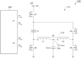
The series capacitor step-down converter 100 includes a main circuit 110 and a controller integrated circuit (IC) 200. The controller IC 200 is an application specific integrated circuit (ASIC) integrated on one semiconductor substrate.
The main circuit 110 includes a first switch S1 to a fourth switch S4, a coupled inductor 112, a series capacitor Cr, and an output capacitor Cout.
The first switch S1 has a first end connected to the input line 102. The coupled inductor 112 is a transformer and includes a first inductor L1 and a second inductor L2 that are magnetically coupled. The first inductor L1 and the second inductor L2 have equal inductance L, and further have mutual inductance M. A first end of each of the first inductor L1 and the second inductor L2 is connected between the output line 104 and ground.
The second switch S2 is connected between a second end of the first inductor L1 and ground. The series capacitor Cr is connected between a second end of the first switch S1 and the second end of the first inductor L1. The third switch S3 is connected between the second end of the first switch S1 and a second end of the second inductor L2. The fourth switch S4 is connected between the second end of the second inductor L2 and ground. The output capacitor Cout is connected to the output line 104.
In this example, the first switch S1 to the fourth switch S4 are all illustrated as N-channel metal-oxide-semiconductor field-effect transistors (MOSFETs), but are not limited thereto, and other transistors may be used. Also, the second switch S2 and the fourth switch S4 on the low side may be rectifying elements such as diodes.
The controller IC 200 controls the first switch S1 to the fourth switch S4 to generate the output voltage Vout on the output line 104. To be specific, the controller IC 200 alternately repeats a first state φ1 and a second state φ2 at a predetermined switching frequency fsw with a dead time TD interposed therebetween.
-
- First state φ1:
- First switch S1=ON
- Second switch S2=OFF
- Third switch S3=OFF
- Fourth switch S4=ON
- Second state φ2:
- First switch S1=OFF
- Second switch S2=ON
- Third switch S3=ON
- Fourth switch S4=OFF
- Dead time TD:
- First switch S1=OFF
- Second switch S2=OFF
- Third switch S3=OFF
- Fourth switch S4=OFF
When the length of each of the first state φ1 and the second state φ2 is TON, the switching frequency fsw is 1/(2×TON). In other words, operating at the switching frequency fsw means repeating the first state φ1 and the second state φ2 at intervals of TON=1/(2×fsw).
The abovementioned configuration is the configuration of the series capacitor step-down converter 100. Next, the operation thereof will be described.
In the first state φ1, the series capacitor Cr, the first inductor L1 (leakage inductance Lk), and the output capacitor Cout form a series resonance circuit, and a resonance current Ires flows through the first inductor L1 (IL1=Ires). Since the total current of the resonance current Ires′, which is a replica of the resonance current Ires flowing through the first inductor L1, and the exciting current Im2 flowing through the exciting inductance Lm flows through the second inductor L2, the second coil current IL2 satisfies IL2=Ires′+Im2.
In the second state φ2, the series capacitor Cr, the leakage inductance Lk, and the output capacitor Cout form a series resonance circuit, and the resonance current Ires flows through the second inductor L2 (IL2=Ires). Since the total current of the resonance current Ires′, which is a replica of the resonance current Ires flowing through the second inductor L2, and an exciting current Im1 flowing through the exciting inductance Lm flows through the first inductor L1, the first coil current IL1 satisfies IL1=Ires′+Im1.
When the first state φ1 and the second state φ2 are alternately repeated, the voltage across the series capacitor Cr becomes Vin/2 in the steady state, and the remaining Vin/2 is applied to the coupled inductor 112. When the inductances of the first inductor L1 and the second inductor L2 are equal, an output voltage Vout that is ¼ times Vin is generated on the output line 104.
The conditions for the series capacitor step-down converter 100 to perform ZVS are as follows.
-
- Transition from the first state φ1 to the second state φ2
During the dead time TD immediately after the first state φ1, when IL10 is satisfied, the current IL1 flows through the body diode of the second switch S2, and the voltage across the second switch S2 decreases. At this time, when the state is changed to the second state φ2, that is, when the second switch S2 is turned on, the ZVS of the second switch S2 is established. It should be noted that the direction toward the output line 104 for the currents IL1 and IL2 is regarded as the positive direction.
Further during the dead time TD, when IL2<0 is satisfied, the voltage at the connection node between the third switch S3 and the fourth switch S4 increases due to the regenerative current, and the voltage across the third switch S3 decreases. At this time, when the state is changed to the second state φ2, that is, when the third switch S3 is turned on, the ZVS of the third switch S3 is established.
-
- Transition from the second state φ2 to the first state φ1
During the dead time TD immediately after the second state φ2, when IL1<0 is satisfied, the voltage at the connection node between the first switch S1 and the second switch S2 increases due to the regenerative current, and the voltage across the first switch S1 decreases. At this time, when the state is changed to the first state φ1, that is, when the first switch S1 is turned on, the ZVS of the first switch S1 is established.
Further, during the dead time, when IL2≥0 is satisfied, the current IL2 flows through the body diode of the fourth switch S4, and the voltage across the fourth switch S4 is small. At this time, when the state is changed to the first state φ1, that is, when the fourth switch S4 is turned on, the ZVS of the fourth switch S4 is established.
At the timing of the end of the first state φ1, since the current IL1 of the first inductor L1 is positive or zero (IL1>0), and the current IL2 of the second inductor L2 is negative (IL2<0), the ZVS conditions mentioned above is satisfied.
Similarly, at the timing of the end of the second state φ2, the current IL1 through the first inductor L1 is negative (IL1<0) and the current IL2 through the second inductor L2 is positive or zero (IL2≥0), so that the ZVS conditions mentioned above is satisfied.
Thus, the series capacitor step-down converter 100 can satisfy the ZVS conditions by switching at the resonance frequency fr, and can operate with high efficiency.
A resonance frequency fr1 in the first state φ1 of the main circuit 110 is represented by Equation (2).
Similarly, a resonance frequency fr2 in the second state φ2 of the main circuit 110 is represented by Equation (3).
A situation satisfying fr1=fr2 is ideal, but since the main circuit 110 is mounted on a printed substrate, its resonance frequencies fr1 and fr2 are affected by parasitic capacitance and parasitic inductance, so that it is not easy to make the frequencies agree with each other perfectly. Further, among the components of the main circuit 110, inductors (transformers) and capacitors are mounted as chip components, and their circuit constants vary. Therefore, it is not easy to completely match (tune) the switching frequency with the resonance frequency for each series capacitor step-down converter 100.
When the switching frequency of the series capacitor step-down converter 100 is made to agree with the design value of the resonance frequency of the main circuit 110, depending on the combination of variations in circuit constants, a situation occurs in which the switching frequency may become lower than the resonance frequency, in other words, the on-time TON in the first state φ1 and the second state φ2 is longer than half the resonance time (resonance half-cycle) Tr/2.
Referring to FIG. 6 , if TON is too long compared to the resonance half-cycle Tr/2, the first coil current IL1 becomes a negative current at the timing of transition from the first state φ1 to the second state φ2, and thus the ZVS conditions are not satisfied.
On the other hand, when the switching frequency fsw is high (the top in the figure), in other words, when the on-time TON becomes short, the current IL1 of the first inductor L1 and the current IL2 of the second inductor L2 will both be positive at the timing of transition to the dead time TD. In this case, by lengthening the dead time TD, a state of IL1>0 and IL2<0 can be created, and the ZVS conditions can be satisfied.
In the present embodiment, by utilizing this property, the switching frequency fsw is set high in advance so that the switching frequency fsw is higher than the resonance frequency fr even when the resonance frequency fr is lowered. The length of the dead time TD should be determined so as to satisfy the ZVS conditions when the resonance frequency fr takes the lowest value in the assumed range.
To be specific, the switching frequency fsw is set higher than the frequency f0 determined by Equation (4).
L is the design value of the inductance of the first inductor L1 and the second inductor L2, M is the design value of the mutual inductance of the first inductor L1 and the second inductor L2, and Cr is the design value of the capacitance of the series capacitor.
For example, the switching frequency fsw may range from 1.05 to 1.3 times the frequency f0. More preferably, the switching frequency fsw can be set within a range of 1.1 to 1.2 times the frequency f0. Within this range, even if the resonance frequency varies, the ZVS conditions can be satisfied with a realistic dead time TD.
In a region where the output power Po is small, the efficiency can be further improved by making the switching frequency f sw higher than the resonance frequency.
(Application)
In recent years, there has been a movement to replace the bus voltage from 12 V to 48 V in order to reduce the current flowing through the wires. In this case, a power supply circuit 720 for stepping down the power supply voltage of 48 V to 12 V is required. The above-described series capacitor step-down converter 100 with ¼ gain can be suitably used for such a power supply circuit 720.
The electronic device 700 is not limited to a server and may be an in-vehicle device. Automobile batteries in the past are for mainly 12 V or 24 V, but for hybrid vehicles, there are cases where a 48 V system may be adopted, and also in this case, a power supply circuit that converts the battery voltage from 48 V to 12 V is required. In such a case, the series capacitor step-down converter 100 with ¼ gain can be preferably used.
In addition, the electronic device 700 may be industrial equipment, office automation (OA) equipment, or consumer equipment such as audio equipment.
The embodiments are examples, and it is understood by those skilled in the art that there are various modifications in the combination of respective components and processing processes, and such modifications are also included in the present disclosure and can constitute the scope of the present disclosure.
According to certain aspects of the present disclosure, power conversion efficiency can be improved.
Claims (8)
1. A controller circuit for a series capacitor step-down converter that drives a plurality of switching elements of the series capacitor step-down converter at a switching frequency fsw higher than a frequency f0 represented by the following Equation
wherein
L is a design value for an inductance value of each inductor of at least two inductors constituting a coupled inductor of the series capacitor step-down converter,
M is a design value for a mutual inductance of the at least two inductors, and
Cr is a design value of a capacitance of a series capacitor of the series capacitor step-down converter.
2. The controller circuit according to claim 1 , wherein the switching frequency fsw is in a range of 1.05 to 1.3 times the frequency f0.
3. The controller circuit according to claim 1 , wherein the switching frequency fsw is in a range of 1.1 to 1.2 times the frequency f0.
4. The controller circuit according to claim 1 , wherein the controller circuit is monolithically integrated on one semiconductor substrate.
5. A series capacitor step-down converter comprising:
a main circuit of the series capacitor step-down converter; and
the controller circuit according to claim 1 wherein
the main circuit includes the plurality of switching elements.
6. A method for controlling a series capacitor step-down converter, the series capacitor step-down converter including
an input line and an output line,
a first switch having a first end and a second end, wherein
the first end of the first switch is connected to the input line,
a coupled inductor including a first inductor and a second inductor which are coupled with each other with a mutual inductance design value of M, wherein
each of the first inductor and the second inductor has a first end and a second end, and
the first end of each of the first inductor and the second inductor is connected to the output line,
a second switch connected between the second end of the first inductor and ground,
a series capacitor connected between the second end of the first switch and the second end of the first inductor,
a third switch connected between the second end of the first switch and the second end of the second inductor,
a fourth switch connected between the second end of the second inductor and ground, and
an output capacitor connected to the output line, the method comprising:
defining a switching frequency fsw higher than a frequency f0 represented by the following Equation
wherein
L is a design value for an inductance value for each of the first inductor and the second inductor,
M is the mutual inductance design value for a mutual inductance of the first inductor and the second inductor, and
Cr is a design value of a capacitance of the series capacitor; and
repeating a first state in which the first switch and the fourth switch are on and a second state in which the second switch and the third switch are on, which have same duration, at the switching frequency fsw.
7. The method for controlling according to claim 6 , wherein the switching frequency fsw is in a range of 1.05 to 1.3 times the frequency f0.
8. The method for controlling according to claim 6 , wherein the switching frequency fsw is in a range of 1.1 to 1.2 times the frequency f0.
Applications Claiming Priority (2)
| Application Number | Priority Date | Filing Date | Title |
|---|---|---|---|
| JP2022-112743 | 2022-07-13 | ||
| JP2022112743A JP2024011059A (en) | 2022-07-13 | 2022-07-13 | Series capacitor buck converter and its controller circuit and control method |
Publications (2)
| Publication Number | Publication Date |
|---|---|
| US20240022159A1 US20240022159A1 (en) | 2024-01-18 |
| US12348119B2 true US12348119B2 (en) | 2025-07-01 |
Family
ID=89509313
Family Applications (1)
| Application Number | Title | Priority Date | Filing Date |
|---|---|---|---|
| US18/350,243 Active 2043-09-26 US12348119B2 (en) | 2022-07-13 | 2023-07-11 | Series capacitor step-down converter, and controller circuit and control method thereof |
Country Status (2)
| Country | Link |
|---|---|
| US (1) | US12348119B2 (en) |
| JP (1) | JP2024011059A (en) |
Citations (7)
| Publication number | Priority date | Publication date | Assignee | Title |
|---|---|---|---|---|
| US20150162840A1 (en) * | 2010-02-18 | 2015-06-11 | Arda Power Inc | Dc-dc converter circuit using an llc circuit in the region of voltage gain above unity |
| JP2017147893A (en) * | 2016-02-18 | 2017-08-24 | 住友電気工業株式会社 | DC-DC converter |
| US20180041120A1 (en) * | 2016-08-03 | 2018-02-08 | Schneider Electric It Corporation | High step down dc/dc converter |
| US20210288581A1 (en) * | 2020-03-16 | 2021-09-16 | The Regents Of The University Of Colorado, A Body Corporate | Transformerless Stacked Active Bridge Power Converters And Methods For Operating The Same |
| CN113726167A (en) * | 2021-05-19 | 2021-11-30 | 电子科技大学 | Mixed fixed frequency modulation method with wide output gain range |
| US11329546B2 (en) * | 2018-07-19 | 2022-05-10 | Omron Corporation | Power converter apparatus provided with low-pass filter circuit for reducing switching frequency components |
| US20220247303A1 (en) * | 2021-02-04 | 2022-08-04 | Delta Electronics, Inc. | Power conversion circuit |
-
2022
- 2022-07-13 JP JP2022112743A patent/JP2024011059A/en active Pending
-
2023
- 2023-07-11 US US18/350,243 patent/US12348119B2/en active Active
Patent Citations (7)
| Publication number | Priority date | Publication date | Assignee | Title |
|---|---|---|---|---|
| US20150162840A1 (en) * | 2010-02-18 | 2015-06-11 | Arda Power Inc | Dc-dc converter circuit using an llc circuit in the region of voltage gain above unity |
| JP2017147893A (en) * | 2016-02-18 | 2017-08-24 | 住友電気工業株式会社 | DC-DC converter |
| US20180041120A1 (en) * | 2016-08-03 | 2018-02-08 | Schneider Electric It Corporation | High step down dc/dc converter |
| US11329546B2 (en) * | 2018-07-19 | 2022-05-10 | Omron Corporation | Power converter apparatus provided with low-pass filter circuit for reducing switching frequency components |
| US20210288581A1 (en) * | 2020-03-16 | 2021-09-16 | The Regents Of The University Of Colorado, A Body Corporate | Transformerless Stacked Active Bridge Power Converters And Methods For Operating The Same |
| US20220247303A1 (en) * | 2021-02-04 | 2022-08-04 | Delta Electronics, Inc. | Power conversion circuit |
| CN113726167A (en) * | 2021-05-19 | 2021-11-30 | 电子科技大学 | Mixed fixed frequency modulation method with wide output gain range |
Non-Patent Citations (2)
| Title |
|---|
| Stefano Saggini, Shuai Jiang, Mario Ursino, Chenhao Nan, ‘A 99% Efficient Dual-Phase Resonant SwitchedCapacitor-Buck Converter for 48 V Data Center Bus Conversions,’ 2019 IEEE Applied Power Electronics Conference and Exposition (APEC). https://www.semanticscholar.org/paper/A-99-Efficient-Dual-Phase-Resonant-Converter-for-48-SagginiJiang/5a7627a49f99c71b67007a8df1eff7b8a766f22b. |
| Stefano Saggini; Shuai Jiang; Mario Ursino; Chenhao Nan; "A 99% Efficient Dual-Phase Resonant Switched-Capacitor-Buck Converter for 48 V Data Center Bus Conversions"; May 27, 2019; IEEE; 2019 IEEE Applied Power Electronics Conference and Exposition (APEC) (Year: 2019). * |
Also Published As
| Publication number | Publication date |
|---|---|
| US20240022159A1 (en) | 2024-01-18 |
| JP2024011059A (en) | 2024-01-25 |
Similar Documents
| Publication | Publication Date | Title |
|---|---|---|
| US6549436B1 (en) | Integrated magnetic converter circuit and method with improved filtering | |
| US11469674B2 (en) | Resonant DC-DC converter | |
| US7760525B2 (en) | Voltage regulator | |
| US10263528B2 (en) | Resonant converter with adaptive switching frequency and the method thereof | |
| CN103503292B (en) | Power-converting device and possess the vehicular electric power source device of this power-converting device | |
| US10211734B1 (en) | Bidirectional DC-DC converter | |
| CN111756243B (en) | Resonant Switched Capacitor Converter | |
| US20220286061A1 (en) | Power conversion circuit and power conversion device | |
| US12155303B2 (en) | Switching converter including controller circuit driving switches | |
| US7683590B2 (en) | Step-down switching DC-DC converter | |
| US20050285585A1 (en) | DC-DC converter | |
| US10348205B1 (en) | Coupled-inductor cascaded buck converter with fast transient response | |
| JP2004208448A (en) | Buck-boost DC-DC converter | |
| US11863080B2 (en) | Active-clamped isolated sepic converter in the MHz range for low-power subnets | |
| US12348119B2 (en) | Series capacitor step-down converter, and controller circuit and control method thereof | |
| US12395077B2 (en) | Series capacitor step-down converter, controller circuit thereof, and control method | |
| US12431803B2 (en) | Series capacitor buck converter and controller circuit and control method thereof | |
| CN112400273B (en) | Switching Power Supply | |
| US20240006981A1 (en) | Series capacitor step-down converter as well as controller circuit and control method thereof | |
| JP2001309646A (en) | Switching power supply | |
| JP3069565B1 (en) | Switching power supply | |
| JP2024024527A (en) | Series capacitor buck converter and controller circuit thereof and control method | |
| JP2024006793A (en) | Series capacitor step-down converter, and controller circuit and control method thereof | |
| EP1808952B1 (en) | Voltage regulator | |
| JP2024020025A (en) | Series capacitor step-down converter, controller circuit therefor, and control method |
Legal Events
| Date | Code | Title | Description |
|---|---|---|---|
| FEPP | Fee payment procedure |
Free format text: ENTITY STATUS SET TO UNDISCOUNTED (ORIGINAL EVENT CODE: BIG.); ENTITY STATUS OF PATENT OWNER: LARGE ENTITY |
|
| STPP | Information on status: patent application and granting procedure in general |
Free format text: DOCKETED NEW CASE - READY FOR EXAMINATION |
|
| STPP | Information on status: patent application and granting procedure in general |
Free format text: NON FINAL ACTION MAILED |
|
| STPP | Information on status: patent application and granting procedure in general |
Free format text: RESPONSE TO NON-FINAL OFFICE ACTION ENTERED AND FORWARDED TO EXAMINER |
|
| STPP | Information on status: patent application and granting procedure in general |
Free format text: NOTICE OF ALLOWANCE MAILED -- APPLICATION RECEIVED IN OFFICE OF PUBLICATIONS |
|
| STCF | Information on status: patent grant |
Free format text: PATENTED CASE |