US12328071B2 - Bidirectional direct current converter and control method thereof - Google Patents
Bidirectional direct current converter and control method thereof Download PDFInfo
- Publication number
- US12328071B2 US12328071B2 US18/063,321 US202218063321A US12328071B2 US 12328071 B2 US12328071 B2 US 12328071B2 US 202218063321 A US202218063321 A US 202218063321A US 12328071 B2 US12328071 B2 US 12328071B2
- Authority
- US
- United States
- Prior art keywords
- switching transistor
- direct current
- drive signal
- drive
- cycle
- Prior art date
- Legal status (The legal status is an assumption and is not a legal conclusion. Google has not performed a legal analysis and makes no representation as to the accuracy of the status listed.)
- Active, expires
Links
Images


Classifications
-
- H—ELECTRICITY
- H02—GENERATION; CONVERSION OR DISTRIBUTION OF ELECTRIC POWER
- H02M—APPARATUS FOR CONVERSION BETWEEN AC AND AC, BETWEEN AC AND DC, OR BETWEEN DC AND DC, AND FOR USE WITH MAINS OR SIMILAR POWER SUPPLY SYSTEMS; CONVERSION OF DC OR AC INPUT POWER INTO SURGE OUTPUT POWER; CONTROL OR REGULATION THEREOF
- H02M3/00—Conversion of DC power input into DC power output
- H02M3/02—Conversion of DC power input into DC power output without intermediate conversion into AC
- H02M3/04—Conversion of DC power input into DC power output without intermediate conversion into AC by static converters
- H02M3/10—Conversion of DC power input into DC power output without intermediate conversion into AC by static converters using discharge tubes with control electrode or semiconductor devices with control electrode
- H02M3/145—Conversion of DC power input into DC power output without intermediate conversion into AC by static converters using discharge tubes with control electrode or semiconductor devices with control electrode using devices of a triode or transistor type requiring continuous application of a control signal
- H02M3/155—Conversion of DC power input into DC power output without intermediate conversion into AC by static converters using discharge tubes with control electrode or semiconductor devices with control electrode using devices of a triode or transistor type requiring continuous application of a control signal using semiconductor devices only
- H02M3/156—Conversion of DC power input into DC power output without intermediate conversion into AC by static converters using discharge tubes with control electrode or semiconductor devices with control electrode using devices of a triode or transistor type requiring continuous application of a control signal using semiconductor devices only with automatic control of output voltage or current, e.g. switching regulators
- H02M3/158—Conversion of DC power input into DC power output without intermediate conversion into AC by static converters using discharge tubes with control electrode or semiconductor devices with control electrode using devices of a triode or transistor type requiring continuous application of a control signal using semiconductor devices only with automatic control of output voltage or current, e.g. switching regulators including plural semiconductor devices as final control devices for a single load
-
- H—ELECTRICITY
- H02—GENERATION; CONVERSION OR DISTRIBUTION OF ELECTRIC POWER
- H02M—APPARATUS FOR CONVERSION BETWEEN AC AND AC, BETWEEN AC AND DC, OR BETWEEN DC AND DC, AND FOR USE WITH MAINS OR SIMILAR POWER SUPPLY SYSTEMS; CONVERSION OF DC OR AC INPUT POWER INTO SURGE OUTPUT POWER; CONTROL OR REGULATION THEREOF
- H02M1/00—Details of apparatus for conversion
- H02M1/0003—Details of control, feedback or regulation circuits
- H02M1/0032—Control circuits allowing low power mode operation, e.g. in standby mode
- H02M1/0035—Control circuits allowing low power mode operation, e.g. in standby mode using burst mode control
-
- H—ELECTRICITY
- H02—GENERATION; CONVERSION OR DISTRIBUTION OF ELECTRIC POWER
- H02M—APPARATUS FOR CONVERSION BETWEEN AC AND AC, BETWEEN AC AND DC, OR BETWEEN DC AND DC, AND FOR USE WITH MAINS OR SIMILAR POWER SUPPLY SYSTEMS; CONVERSION OF DC OR AC INPUT POWER INTO SURGE OUTPUT POWER; CONTROL OR REGULATION THEREOF
- H02M1/00—Details of apparatus for conversion
- H02M1/0048—Circuits or arrangements for reducing losses
- H02M1/0054—Transistor switching losses
-
- H—ELECTRICITY
- H02—GENERATION; CONVERSION OR DISTRIBUTION OF ELECTRIC POWER
- H02M—APPARATUS FOR CONVERSION BETWEEN AC AND AC, BETWEEN AC AND DC, OR BETWEEN DC AND DC, AND FOR USE WITH MAINS OR SIMILAR POWER SUPPLY SYSTEMS; CONVERSION OF DC OR AC INPUT POWER INTO SURGE OUTPUT POWER; CONTROL OR REGULATION THEREOF
- H02M3/00—Conversion of DC power input into DC power output
- H02M3/22—Conversion of DC power input into DC power output with intermediate conversion into AC
- H02M3/24—Conversion of DC power input into DC power output with intermediate conversion into AC by static converters
- H02M3/28—Conversion of DC power input into DC power output with intermediate conversion into AC by static converters using discharge tubes with control electrode or semiconductor devices with control electrode to produce the intermediate AC
- H02M3/325—Conversion of DC power input into DC power output with intermediate conversion into AC by static converters using discharge tubes with control electrode or semiconductor devices with control electrode to produce the intermediate AC using devices of a triode or a transistor type requiring continuous application of a control signal
- H02M3/335—Conversion of DC power input into DC power output with intermediate conversion into AC by static converters using discharge tubes with control electrode or semiconductor devices with control electrode to produce the intermediate AC using devices of a triode or a transistor type requiring continuous application of a control signal using semiconductor devices only
- H02M3/33569—Conversion of DC power input into DC power output with intermediate conversion into AC by static converters using discharge tubes with control electrode or semiconductor devices with control electrode to produce the intermediate AC using devices of a triode or a transistor type requiring continuous application of a control signal using semiconductor devices only having several active switching elements
- H02M3/33576—Conversion of DC power input into DC power output with intermediate conversion into AC by static converters using discharge tubes with control electrode or semiconductor devices with control electrode to produce the intermediate AC using devices of a triode or a transistor type requiring continuous application of a control signal using semiconductor devices only having several active switching elements having at least one active switching element at the secondary side of an isolation transformer
- H02M3/33584—Bidirectional converters
-
- H—ELECTRICITY
- H02—GENERATION; CONVERSION OR DISTRIBUTION OF ELECTRIC POWER
- H02M—APPARATUS FOR CONVERSION BETWEEN AC AND AC, BETWEEN AC AND DC, OR BETWEEN DC AND DC, AND FOR USE WITH MAINS OR SIMILAR POWER SUPPLY SYSTEMS; CONVERSION OF DC OR AC INPUT POWER INTO SURGE OUTPUT POWER; CONTROL OR REGULATION THEREOF
- H02M7/00—Conversion of AC power input into DC power output; Conversion of DC power input into AC power output
- H02M7/42—Conversion of DC power input into AC power output without possibility of reversal
- H02M7/44—Conversion of DC power input into AC power output without possibility of reversal by static converters
- H02M7/48—Conversion of DC power input into AC power output without possibility of reversal by static converters using discharge tubes with control electrode or semiconductor devices with control electrode
- H02M7/483—Converters with outputs that each can have more than two voltages levels
- H02M7/4837—Flying capacitor converters
-
- H—ELECTRICITY
- H03—ELECTRONIC CIRCUITRY
- H03K—PULSE TECHNIQUE
- H03K17/00—Electronic switching or gating, i.e. not by contact-making and –breaking
- H03K17/51—Electronic switching or gating, i.e. not by contact-making and –breaking characterised by the components used
- H03K17/56—Electronic switching or gating, i.e. not by contact-making and –breaking characterised by the components used by the use, as active elements, of semiconductor devices
- H03K17/687—Electronic switching or gating, i.e. not by contact-making and –breaking characterised by the components used by the use, as active elements, of semiconductor devices the devices being field-effect transistors
-
- Y—GENERAL TAGGING OF NEW TECHNOLOGICAL DEVELOPMENTS; GENERAL TAGGING OF CROSS-SECTIONAL TECHNOLOGIES SPANNING OVER SEVERAL SECTIONS OF THE IPC; TECHNICAL SUBJECTS COVERED BY FORMER USPC CROSS-REFERENCE ART COLLECTIONS [XRACs] AND DIGESTS
- Y02—TECHNOLOGIES OR APPLICATIONS FOR MITIGATION OR ADAPTATION AGAINST CLIMATE CHANGE
- Y02B—CLIMATE CHANGE MITIGATION TECHNOLOGIES RELATED TO BUILDINGS, e.g. HOUSING, HOUSE APPLIANCES OR RELATED END-USER APPLICATIONS
- Y02B70/00—Technologies for an efficient end-user side electric power management and consumption
- Y02B70/10—Technologies improving the efficiency by using switched-mode power supplies [SMPS], i.e. efficient power electronics conversion e.g. power factor correction or reduction of losses in power supplies or efficient standby modes
Definitions
- This disclosure relates to the field of energy technologies, and in particular, to a bidirectional direct current converter and a control method thereof in the field of energy technologies.
- a direct current converter is a power electronic apparatus that can convert a direct current of one voltage class into a direct current of another voltage class.
- Direct current converters are usually classified into unidirectional direct current converters and bidirectional direct current converters.
- a unidirectional direct current converter is a direct current converter that can perform only unidirectional power transmission
- a bidirectional direct current converter is a direct current converter that can perform bidirectional power transmission.
- This disclosure provides a bidirectional direct current converter and a control method thereof.
- a controller performs complementary control on a first switching transistor and a third switching transistor, and performs complementary control on a second switching transistor and a fourth switching transistor, to reduce an inductance of an inductor, thereby reducing a size and costs of the inductor, and further reducing a size and costs of the entire bidirectional direct current converter.
- the bidirectional direct current converter may include a first switching transistor, a second switching transistor, a third switching transistor, a fourth switching transistor, a capacitor, an inductor, and a controller.
- the bidirectional direct current converter may include a first direct current terminal, a second direct current terminal, a third direct current terminal, and a fourth direct current terminal.
- the first direct current terminal and the second direct current terminal may constitute an input terminal of the bidirectional direct current converter
- the third direct current terminal and the fourth direct current terminal may constitute an output terminal of the bidirectional direct current converter. Therefore, the bidirectional direct current converter may implement forward power transmission by using the four direct current terminals.
- the third direct current terminal and the fourth direct current terminal may constitute an input terminal of the bidirectional direct current converter
- the first direct current terminal and the second direct current terminal may constitute an output terminal of the bidirectional direct current converter. Therefore, the bidirectional direct current converter may implement reverse power transmission by using the four direct current terminals.
- a first terminal of the inductor may be configured to connect to the first direct current terminal, and a second terminal of the inductor may be configured to connect to a first node.
- a first electrode of the first switching transistor may be configured to connect to the first node, and a second electrode of the first switching transistor may be configured to connect to a second node.
- a first electrode of the second switching transistor may be configured to connect to the second node, and a second electrode of the second switching transistor may be configured to connect to the second direct current terminal and the fourth direct current terminal.
- a first electrode of the third switching transistor may be configured to connect to the first node, and a second electrode of the third switching transistor may be configured to connect to a third node.
- a first electrode of the fourth switching transistor may be configured to connect to the third node, and a second electrode of the fourth switching transistor may be configured to connect to the third direct current terminal.
- a first terminal of the capacitor may be configured to connect to the third node, and a second terminal of the capacitor may be configured to connect to the second node.
- the controller may be configured to connect to the first switching transistor, the second switching transistor, the third switching transistor, and the fourth switching transistor.
- the controller may be configured to perform complementary control on the first switching transistor and the third switching transistor, and perform complementary control on the second switching transistor and the fourth switching transistor.
- the complementary control may be used to indicate that two switching transistors in complementary control cannot be simultaneously turned on or off.
- the first switching transistor and the third switching transistor cannot be simultaneously turned on or off
- the second switching transistor and the fourth switching transistor cannot be simultaneously turned on or off.
- the controller may control the first switching transistor and the third switching transistor not to be simultaneously turned on or off, and the controller may further control the second switching transistor and the fourth switching transistor not to be simultaneously turned on or off.
- the controller may be further configured to control a quantity of on times of the second switching transistor to be greater than a quantity of on times of the first switching transistor in a same cycle. It may also be understood as that, in one cycle, the controller may control a switching frequency of the second switching transistor to be greater than a switching frequency of the first switching transistor, thereby reducing losses of the first switching transistor and the second switching transistor.
- the controller may control the quantity of on times of the second switching transistor to be different from the quantity of on times of the first switching transistor in a same cycle.
- This can increase a quantity of charging and discharging times of the inductor in one cycle, that is, increase a charging and discharging frequency of the inductor. Therefore, the inductor with a small inductance may be used while a same ripple current percentage of the inductor is ensured.
- the inductor with a small inductance has a small size and low costs. This can reduce a size and costs of the bidirectional direct current converter. When the size of the bidirectional direct current converter is reduced, power density of the bidirectional direct current converter can be increased.
- any cycle of the first switching transistor there may be a delay between an on moment of the first switching transistor and an on moment of the second switching transistor. That is, the first switching transistor and the second switching transistor are not simultaneously turned on in any cycle.
- a cycle of the first switching transistor may be the same as a cycle of the third switching transistor.
- the controller is further configured to control a quantity of on times of the fourth switching transistor to be greater than a quantity of on times of the third switching transistor in a same cycle. It may also be understood as that, in one cycle, the controller may control a switching frequency of the fourth switching transistor to be greater than a switching frequency of the third switching transistor, thereby reducing losses of the third switching transistor and the fourth switching transistor.
- the controller controls the quantity of on times of the fourth switching transistor to be different from the quantity of on times of the third switching transistor in a same cycle. Similarly, this can increase a quantity of charging and discharging times of the inductor in one cycle, that is, increase a charging and discharging frequency of the inductor. Therefore, the inductor with a small inductance may be used while a same ripple current percentage of the inductor is ensured. In addition, the inductor with a small inductance has a small size and low costs. This can reduce a size and costs of the bidirectional direct current converter. When the size of the bidirectional direct current converter is reduced, power density of the bidirectional direct current converter can be increased.
- the controller is configured to send a first drive signal to the first switching transistor, send a second drive signal to the second switching transistor, send a third drive signal to the third switching transistor, and send a fourth drive signal to the fourth switching transistor. That is, the controller may send the drive signals to the switching transistors, to implement complementary control on the first switching transistor and the third switching transistor, and implement complementary control on the second switching transistor and the fourth switching transistor.
- the controller sends the first drive signal to the first switching transistor, to control on and off of the first switching transistor.
- the first drive signal may be used to indicate the first switching transistor to be turned on, or the first drive signal may be used to indicate the first switching transistor to be turned off.
- the controller sends the second drive signal to the second switching transistor, to control on and off of the second switching transistor.
- the second drive signal may be used to indicate the second switching transistor to be turned on, or the second drive signal may be used to indicate the second switching transistor to be turned off.
- the controller sends the third drive signal to the third switching transistor, to control on and off of the third switching transistor. It may be understood that the third drive signal may be used to indicate the third switching transistor to be turned on, or the third drive signal may be used to indicate the third switching transistor to be turned off.
- the controller sends the fourth drive signal to the fourth switching transistor, to control on and off of the fourth switching transistor. It may be understood that the fourth drive signal may be used to indicate the fourth switching transistor to be turned on, or the fourth drive signal may be used to indicate the fourth switching transistor to be turned off.
- the first switching transistor when the first drive signal is at a high level, the first switching transistor may be turned on, and when the first drive signal is at a low level, the first switching transistor may be turned off.
- the third switching transistor when the third drive signal is at a high level, the third switching transistor may be turned on, and when the third drive signal is at a low level, the third switching transistor may be turned off.
- the first drive signal may be complementary to the third drive signal. That is, when the first drive signal is at a high level, the third drive signal may be at a low level. Similarly, when the first drive signal is at a low level, the third drive signal may be at a high level.
- the second switching transistor when the second drive signal is at a high level, the second switching transistor may be turned on, and when the second drive signal is at a low level, the second switching transistor may be turned off.
- the fourth switching transistor when the fourth drive signal is at a high level, the fourth switching transistor may be turned on, and when the fourth drive signal is at a low level, the fourth switching transistor may be turned off.
- the second drive signal may be complementary to the fourth drive signal. That is, when the second drive signal is at a high level, the fourth drive signal may be at a low level. Similarly, when the second drive signal is at a low level, the fourth drive signal may be at a high level.
- any cycle of the first switching transistor there may be a delay between the on moment of the first switching transistor and the on moment of the second switching transistor. Therefore, in each cycle of the first drive signal, a rising edge of a first drive pulse of N drive pulses in the second drive signal may be behind the falling edge of the first drive signal. That is, there is a delay time (namely, a delay) between a first drive pulse of two drive pulses in the second drive signal and the first drive signal.
- a rising edge of a first drive pulse of N drive pulses in the fourth drive signal may be in front of a falling edge of the third drive signal. That is, there is a delay between a first drive pulse of two drive pulses in the fourth drive signal and the third drive signal.
- the cycle of the first switching transistor may be the same as the cycle of the third switching transistor. Therefore, a cycle of the first drive signal may be the same as a cycle of the third drive signal.
- the second drive signal may have N drive pulses in each cycle of the first drive signal, that is, the second drive signal and the first drive signal may be two asymmetric drive signals.
- the fourth drive signal may have N drive pulses in each cycle of the third drive signal, that is, the fourth drive signal pulse-width modulation (PWM) and the third drive signal PWM are two asymmetric drive signals.
- PWM pulse-width modulation
- the inductor may have N+1 charging and discharging cycles in each cycle of the first drive signal or the third drive signal, where N is an integer greater than or equal to 2 (for example, N is greater than 3).
- the inductor has at least three charging and discharging cycles in each cycle.
- the controller increases a charging and discharging frequency of the inductor in each cycle (namely, frequency increase), thereby reducing the inductance of the inductor, and reducing the size and the costs of the inductor.
- the second drive signal may have N drive pulses in each cycle of the first drive signal, a cycle of the second drive signal is different from the cycle of the first drive signal.
- the fourth drive signal may also have N drive pulses in each cycle of the third drive signal, a cycle of the fourth drive signal is different from the cycle of the third drive signal.
- the controller may send the first drive signal and the second drive signal that are asymmetric to the first switching transistor and the second switching transistor, and send the third drive signal and the fourth drive signal that are asymmetric to the third switching transistor and the fourth switching transistor, so that a quantity of charging and discharging times of the inductor in each cycle of the first drive signal or the third drive signal is increased, that is, the charging and discharging frequency of the inductor is increased. Therefore, the inductor with a small inductance may be used while a same ripple current percentage of the inductor is ensured. In addition, the inductor with a small inductance has a small size and low costs. This can reduce a size and costs of the bidirectional direct current converter. When the size of the bidirectional direct current converter is reduced, power density of the bidirectional direct current converter can be increased.
- the asymmetric drive signals are sent to the first switching transistor and the second switching transistor, and the asymmetric drive signals are sent to the third switching transistor and the fourth switching transistor, so that a state of the first switching transistor is opposite to a state of the third switching transistor (that is, the first switching transistor is complementary to the third switching transistor), and a state of the second switching transistor is opposite to a state of the fourth switching transistor (that is, the second switching transistor is complementary to the fourth switching transistor).
- current sharing or complement is implemented between a branch in which the first switching transistor and the second switching transistor are located and a branch in which the third switching transistor and the fourth switching transistor are located (that is, between two branches), so that a voltage of the capacitor remains stable.
- the N drive pulses in the second drive signal may be in low level time periods of each cycle of the first drive signal.
- the N drive pulses in the second drive signal may alternatively be in high level time periods of each cycle of the first drive signal.
- the N drive pulses in the second drive signal may be divided into a first part of drive pulses and a second part of drive pulses.
- the first part of drive pulses may be in low level time periods of each cycle of the first drive signal
- the second part of drive pulses may be in high level time periods of each cycle of the first drive signal. This is not limited in this disclosure.
- the N drive pulses in the fourth drive signal may be divided into a first part of drive pulses and a second part of drive pulses.
- the first part of drive pulses may be in low level time periods of each cycle of the third drive signal, and the second part of drive pulses may be in high level time periods of each cycle of the third drive signal.
- the N drive pulses in the fourth drive signal may be all in low level time periods of each cycle of the third drive signal, or may be all in high level time periods of each cycle of the third drive signal. This is not limited in this disclosure.
- frequencies corresponding to at least two of the N drive pulses in the second drive signal or the fourth drive signal may be different.
- a frequency of a drive pulse is inversely proportional to a cycle of the drive pulse. Therefore, cycles corresponding to the at least two of the N drive pulses in the second drive signal or the fourth drive signal are different, so that the frequencies corresponding to the at least two of the N drive pulses in the second drive signal or the fourth drive signal are different.
- a frequency corresponding to each of the N drive pulses in the second drive signal or the fourth drive signal may be different.
- pulse widths and frequencies that are of different drive pulses of the N drive pulses in the second drive signal or the fourth drive signal there is no correspondence between pulse widths and frequencies that are of different drive pulses of the N drive pulses in the second drive signal or the fourth drive signal. That is, when pulse widths of different drive pulses are the same, frequencies of the different drive pulses may be the same or different. Similarly, when frequencies of different drive pulses are the same, pulse widths of the different drive pulses may be the same or different.
- frequencies of first N ⁇ 1 drive pulses of the N drive pulses in the second drive signal or the fourth drive signal may be the same, and a frequency of a last drive pulse of the N drive pulses in the second drive signal may be less than the frequencies of the first N ⁇ 1 drive pulses.
- a time between a rising edge of the first drive signal and the rising edge of the first drive pulse of the N drive pulses in the second drive signal may be a lag time.
- a time between the rising edge of the third drive signal and the rising edge of the first drive pulse of the N drive pulses in the fourth drive signal may be a lag time.
- the lag time may alternatively be defined in another manner. This is not limited in this disclosure.
- the controller may obtain the lag time based on the ripple current of the inductor.
- the controller may control a charging current of the inductor to be equal to a discharging current of the inductor to obtain the lag time.
- the controller may control the charging current of the inductor to be equal to the discharging current of the inductor to obtain the lag time.
- the controller may obtain the lag time based on a first voltage of the bidirectional direct current converter, a second voltage of the bidirectional direct current converter, the voltage of the capacitor, and the cycle of the first drive signal/the third drive signal.
- the first voltage may be used to indicate an input voltage of the bidirectional direct current converter, and the second voltage may be used to indicate an output voltage of the bidirectional direct current converter.
- the first voltage may be used to indicate an output voltage of the bidirectional direct current converter, and the second voltage may be used to indicate an input voltage of the bidirectional direct current converter.
- V 1 may represent the first voltage of the bidirectional direct current converter
- V 2 may represent the second voltage of the bidirectional direct current converter
- V c may represent the voltage of the capacitor
- T sw may represent the cycle of the first drive signal or the third drive signal
- D 1 may represent a duty cycle of the first drive signal
- D 2 T sw may represent the delay time between the rising edge of the first drive pulse of the N drive pulses in the second drive signal and the falling edge of the first drive signal.
- the controller may obtain the lag time based on the loss of the first switching transistor and/or the loss of the second switching transistor, or may obtain the lag time based on the loss of the third switching transistor and/or the loss of the fourth switching transistor.
- the controller may obtain the lag time based on only the loss of the first switching transistor, based on only the loss of the second switching transistor, or based on both the loss of the first switching transistor and the loss of the second switching transistor.
- the controller may obtain the lag time based on only the loss of the third switching transistor, based on only the loss of the fourth switching transistor, or based on both the loss of the third switching transistor and the loss of the fourth switching transistor.
- the controller may obtain the lag time based on the ripple current of the inductor and the loss of at least one of the first switching transistor and the second switching transistor (namely, the loss of the first switching transistor and/or the loss of the second switching transistor), or may obtain the lag time based on the ripple current of the inductor and the loss of at least one of the third switching transistor and the fourth switching transistor (namely, the loss of the third switching transistor and/or the loss of the fourth switching transistor).
- the lag time may alternatively be obtained by using another process in this disclosure. This is not limited in this disclosure.
- a loss generated by the bidirectional direct current converter may be reduced based on losses of different switching transistors, thereby improving conversion efficiency of the bidirectional direct current converter.
- the bidirectional direct current converter provided in this disclosure may further include a fifth switching transistor.
- a first terminal of the fifth switching transistor may be configured to connect to the second terminal of the capacitor, and a second terminal of the fifth switching transistor may be configured to connect to the second node.
- the fifth switching transistor may use an insulated gate field-effect transistor, an insulated gate bipolar transistor, a bidirectional switch, or the like.
- the fifth switching transistor may alternatively use another type of controllable power device.
- a type of the fifth switching transistor is not limited in this disclosure.
- the fifth switching transistor is turned on and off, to protect the second switching transistor from being damaged due to excessively large voltage stress.
- the bidirectional direct current converter provided in this disclosure may further include a first diode and a second diode.
- an anode of the first diode may be configured to connect to the second node
- a cathode of the first diode may be configured to connect to a midpoint of the second voltage
- an anode of the second diode may be configured to connect to the midpoint of the second voltage
- a cathode of the second diode may be configured to connect to the third node.
- a function of the first diode is to clamp a voltage drop borne by the second switching transistor, to prevent the second switching transistor from bearing a voltage of an entire direct current bus when the fourth switching transistor is turned on.
- a function of the second diode is to clamp a voltage drop borne by the fourth switching transistor, to prevent the fourth switching transistor from bearing a voltage of an entire direct current bus when the second switching transistor is turned on. Therefore, the first diode and the second diode may be referred to as clamping diodes.
- first switching transistor, the second switching transistor, the third switching transistor, and the fourth switching transistor separately use any one of the insulated gate field-effect transistor, the insulated gate bipolar transistor, and the bidirectional switch.
- the first diode and the second diode each may alternatively be replaced with another type of power device.
- the controller only needs to send corresponding drive signals, so that the switching transistors implement working modes of the diodes. Details are not described in this disclosure again.
- this disclosure provides an electronic device.
- the electronic device may include a bidirectional direct current converter.
- the bidirectional direct current converter refer to the foregoing descriptions. Details are not described in this disclosure again.
- the bidirectional direct current converter may include a first switching transistor, a second switching transistor, a third switching transistor, a fourth switching transistor, a capacitor, an inductor, and a controller.
- the bidirectional direct current converter may include a first direct current terminal, a second direct current terminal, a third direct current terminal, and a fourth direct current terminal.
- the first direct current terminal and the second direct current terminal may constitute an input terminal of the bidirectional direct current converter
- the third direct current terminal and the fourth direct current terminal may constitute an output terminal of the bidirectional direct current converter. Therefore, the bidirectional direct current converter may implement forward power transmission by using the four direct current terminals.
- the third direct current terminal and the fourth direct current terminal may constitute an input terminal of the bidirectional direct current converter
- the first direct current terminal and the second direct current terminal may constitute an output terminal of the bidirectional direct current converter. Therefore, the bidirectional direct current converter may implement reverse power transmission by using the four direct current terminals.
- a first terminal of the inductor may be configured to connect to the first direct current terminal, and a second terminal of the inductor may be configured to connect to a first node.
- a first electrode of the first switching transistor may be configured to connect to the first node, and a second electrode of the first switching transistor may be configured to connect to a second node.
- a first electrode of the second switching transistor may be configured to connect to the second node, and a second electrode of the second switching transistor may be configured to connect to the second direct current terminal and the fourth direct current terminal.
- a first electrode of the third switching transistor may be configured to connect to the first node, and a second electrode of the third switching transistor may be configured to connect to a third node.
- a first electrode of the fourth switching transistor may be configured to connect to the third node, and a second electrode of the fourth switching transistor may be configured to connect to the third direct current terminal.
- a first terminal of the capacitor may be configured to connect to the third node, and a second terminal of the capacitor may be configured to connect to the second node.
- the controller may be configured to connect to the first switching transistor, the second switching transistor, the third switching transistor, and the fourth switching transistor.
- control method of the bidirectional direct current converter may include the following.
- the controller performs complementary control on the first switching transistor and the third switching transistor, and performs complementary control on the second switching transistor and the fourth switching transistor.
- the complementary control is used to indicate that two switching transistors in complementary control cannot be simultaneously turned on or off.
- the first switching transistor and the third switching transistor cannot be simultaneously turned on or off
- the second switching transistor and the fourth switching transistor cannot be simultaneously turned on or off.
- the controller controls a quantity of on times of the second switching transistor to be greater than a quantity of on times of the first switching transistor in a same cycle. It may also be understood as that, in one cycle, the controller may control a switching frequency of the second switching transistor to be greater than a switching frequency of the first switching transistor, thereby reducing losses of the first switching transistor and the second switching transistor.
- the controller controls the quantity of on times of the second switching transistor to be different from the quantity of on times of the first switching transistor in a same cycle.
- This can increase a quantity of charging and discharging times of the inductor in one cycle, that is, increase a charging and discharging frequency of the inductor. Therefore, the inductor with a small inductance may be used while a same ripple current percentage of the inductor is ensured.
- the inductor with a small inductance has a small size and low costs. This can reduce a size and costs of the bidirectional direct current converter. When the size of the bidirectional direct current converter is reduced, power density of the bidirectional direct current converter can be increased.
- any cycle of the first switching transistor there may be a delay between an on moment of the first switching transistor and an on moment of the second switching transistor. That is, the first switching transistor and the second switching transistor are not simultaneously turned on in any cycle.
- a cycle of the first switching transistor may be the same as a cycle of the third switching transistor.
- control method may further include the following.
- the controller controls a quantity of on times of the fourth switching transistor to be greater than a quantity of on times of the third switching transistor in a same cycle. It may also be understood as that, in one cycle, the controller may control a switching frequency of the fourth switching transistor to be greater than a switching frequency of the third switching transistor, thereby reducing losses of the third switching transistor and the fourth switching transistor.
- the controller controls the quantity of on times of the fourth switching transistor to be different from the quantity of on times of the third switching transistor in a same cycle. Similarly, this can increase a quantity of charging and discharging times of the inductor in one cycle, that is, increase a charging and discharging frequency of the inductor. Therefore, the inductor with a small inductance may be used while a same ripple current percentage of the inductor is ensured. In addition, the inductor with a small inductance has a small size and low costs. This can reduce a size and costs of the bidirectional direct current converter. When the size of the bidirectional direct current converter is reduced, power density of the bidirectional direct current converter can be increased.
- FIG. 1 is a schematic diagram of a structure of a bidirectional direct current converter according to an embodiment of this disclosure
- FIG. 2 is a schematic diagram of waveforms of asymmetric drive signals according to an embodiment of this disclosure
- FIG. 3 is a schematic diagram of waveforms of symmetric drive signals according to an embodiment of this disclosure.
- FIG. 4 is a schematic diagram of waveforms of symmetric drive signals according to an embodiment of this disclosure.
- FIG. 6 is a schematic diagram of waveforms of a first drive signal and a second drive signal according to an embodiment of this disclosure
- FIG. 8 is a schematic diagram of waveforms of a first drive signal and a second drive signal according to an embodiment of this disclosure
- FIG. 10 is a schematic diagram of waveforms of a first drive signal and a second drive signal according to an embodiment of this disclosure
- FIG. 11 is a schematic diagram of waveforms of a first drive signal and a second drive signal according to an embodiment of this disclosure
- FIG. 13 is a schematic diagram of a structure of a bidirectional direct current converter according to an embodiment of this disclosure.
- FIG. 14 is a schematic diagram of a structure of a bidirectional direct current converter according to an embodiment of this disclosure.
- FIG. 15 is a schematic diagram of a structure of a bidirectional direct current converter according to an embodiment of this disclosure.
- At least one (item) refers to one or more, and “a plurality of” refers to two or more.
- the term “and/or” is used for describing an association relationship between associated objects, and represents that three relationships may exist.
- a and/or B may represent the following three cases: only A exists, only B exists, and both A and B exist, where A and B may be singular or plural.
- the character “/” usually indicates an “or” relationship between associated objects.
- At least one of the following items (pieces) or a similar expression thereof indicates any combination of these items, including a single item (piece) or any combination of a plurality of items (pieces).
- At least one item (piece) of a, b, or c may represent: a, b, c, “a and b”, “a and c”, “b and c”, or “a, b, and c”, where a, b, and c may be singular or plural.
- the bidirectional direct current converter 1 may include a first switching transistor S 1 , a second switching transistor S 2 , a third switching transistor S 3 , a fourth switching transistor S 4 , a capacitor C (flying capacitor), an inductor L, and a controller (not shown in FIG. 1 ).
- the bidirectional direct current converter 1 may include a first direct current terminal DC 1 , a second direct current terminal DC 2 , a third direct current terminal DC 3 , and a fourth direct current terminal DC 4 .
- the first direct current terminal DC 1 and the second direct current terminal DC 2 may constitute an input terminal of the bidirectional direct current converter 1
- the third direct current terminal DC 3 and the fourth direct current terminal DC 4 may constitute an output terminal of the bidirectional direct current converter 1 . Therefore, in FIG. 1 , V 1 (namely, a first voltage that is a voltage between the first direct current terminal DC 1 and the second direct current terminal DC 2 ) may be used to indicate an input voltage of the bidirectional direct current converter 1
- V 2 namely, a second voltage that is a voltage between the third direct current terminal DC 3 and the fourth direct current terminal DC 4
- the third direct current terminal DC 3 and the fourth direct current terminal DC 4 may constitute an input terminal of the bidirectional direct current converter 1
- the first direct current terminal DC 1 and the second direct current terminal DC 2 may constitute an output terminal of the bidirectional direct current converter 1 . Therefore, in FIG. 1 , V 1 (namely, a first voltage) may be used to indicate an output voltage of the bidirectional direct current converter 1
- V 2 namely, a second voltage
- the bidirectional direct current converter provided in this embodiment of this disclosure can implement bidirectional power transmission.
- a power may be transmitted from the first direct current terminal DC 1 and the second direct current terminal DC 2 that are used as the input terminal to the third direct current terminal DC 3 and the fourth direct current terminal DC 4 that are used as the output terminal, to implement forward power transmission (that is, the bidirectional direct current converter performs forward working).
- a power may alternatively be transmitted from the third direct current terminal DC 3 and the fourth direct current terminal DC 4 that are used as the input terminal to the first direct current terminal DC 1 and the second direct current terminal DC 2 that are used as the output terminal, to implement reverse power transmission (that is, the bidirectional direct current converter performs reverse working).
- a first terminal of the inductor L (namely, a left terminal of the inductor L in FIG. 1 ) may be connected to the first direct current terminal DC 1 , and a second terminal of the inductor L may be connected to a node A (namely, a first node).
- a first electrode of the first switching transistor S 1 (namely, an electrode that is of the first switching transistor S 1 and that is close to the node A in FIG. 1 ) may be connected to the node A
- a second electrode of the first switching transistor S 1 (namely, an electrode that is of the first switching transistor S 1 and that is close to a node B in FIG. 1 ) may be connected to the node B (namely, a second node).
- a first electrode of the second switching transistor S 2 (namely, an electrode that is of the second switching transistor S 2 and that is close to the node B in FIG. 1 ) is connected to the node B, a second electrode of the second switching transistor S 2 (namely, an electrode that is of the second switching transistor S 2 and that is away from the node B in FIG. 1 ) may be connected to a node E, and the node E is connected to the second direct current terminal DC 2 and the fourth direct current terminal DC 4 .
- a first electrode of the third switching transistor S 3 (namely, an electrode that is of the third switching transistor S 3 and that is close to the node A in FIG.
- a second electrode of the third switching transistor S 3 (namely, an electrode that is of the third switching transistor S 3 and that is close to a node D in FIG. 1 ) is connected to the node D (namely, a third node).
- a first electrode of the fourth switching transistor S 4 (namely, an electrode that is of the fourth switching transistor S 4 and that is close to the node D in FIG. 1 ) is connected to the node D, and a second electrode of the fourth switching transistor S 4 (namely, an electrode that is of the fourth switching transistor S 4 and that is close to the third direct current terminal DC 3 in FIG. 1 ) may be connected to the third direct current terminal DC 3 .
- a first terminal of the capacitor C (which may be a positive terminal of the capacitor C) may be connected to the node D, and a second terminal of the capacitor C (which may be a negative terminal of the capacitor C) may be connected to the node B.
- the controller may be connected to the first switching transistor S 1 , the second switching transistor S 2 , the third switching transistor S 3 , and the fourth switching transistor S 4 .
- the bidirectional direct current converter provided in this embodiment of this disclosure is a three-level direct current converter, and three levels are implemented by using a topology of the bidirectional direct current converter.
- voltage stress of a power device may be reduced, so that a high-level voltage output can be implemented by using a power device with a low withstand voltage level.
- the controller may be configured to perform complementary control on the first switching transistor S 1 and the third switching transistor S 3 , and perform complementary control on the second switching transistor S 2 and the fourth switching transistor S 4 .
- the complementary control is used to indicate that two switching transistors in complementary control cannot be simultaneously turned on or off.
- the first switching transistor S 1 and the third switching transistor S 3 cannot be simultaneously turned on or off
- the second switching transistor S 2 and the fourth switching transistor S 4 cannot be simultaneously turned on or off.
- the controller may control the first switching transistor S 1 and the third switching transistor S 3 not to be simultaneously turned on or off, and the controller may further control the second switching transistor S 2 and the fourth switching transistor S 4 not to be simultaneously turned on or off.
- the controller may be further configured to control a quantity of on times of the second switching transistor S 2 to be greater than a quantity of on times of the first switching transistor S 1 in a same cycle. It may also be understood as that, in one cycle, the controller may control a switching frequency of the second switching transistor S 2 to be greater than a switching frequency of the first switching transistor S 1 , thereby reducing losses of the first switching transistor S 1 and the second switching transistor S 2 .
- the controller may control the quantity of on times of the second switching transistor to be different from the quantity of on times of the first switching transistor in a same cycle.
- This can increase a quantity of charging and discharging times of the inductor in one cycle, that is, increase a charging and discharging frequency of the inductor. Therefore, the inductor with a small inductance may be used while a same ripple current percentage of the inductor is ensured.
- the inductor with a small inductance has a small size and low costs. This can reduce a size and costs of the bidirectional direct current converter. When the size of the bidirectional direct current converter is reduced, power density of the bidirectional direct current converter can be increased.
- any cycle of the first switching transistor S 1 there may be a delay between an on moment of the first switching transistor S 1 and an on moment of the second switching transistor S 2 . That is, the first switching transistor S 1 and the second switching transistor S 2 are not simultaneously turned on in any cycle.
- a cycle of the first switching transistor S 1 may be the same as a cycle of the third switching transistor S 3 .
- the controller may be further configured to control a quantity of on times of the fourth switching transistor S 4 to be greater than a quantity of on times of the third switching transistor S 3 in a same cycle. It may also be understood as that, in one cycle, the controller may control a switching frequency of the fourth switching transistor S 4 to be greater than a switching frequency of the third switching transistor S 3 , thereby reducing losses of the fourth switching transistor S 4 and the third switching transistor S 3 .
- the controller controls the quantity of on times of the fourth switching transistor to be different from the quantity of on times of the third switching transistor in a same cycle. Similarly, this can increase a quantity of charging and discharging times of the inductor in one cycle, that is, increase a charging and discharging frequency of the inductor. Therefore, the inductor with a small inductance may be used while a same ripple current percentage of the inductor is ensured. In addition, the inductor with a small inductance has a small size and low costs. This can reduce a size and costs of the bidirectional direct current converter. When the size of the bidirectional direct current converter is reduced, power density of the bidirectional direct current converter can be increased.
- the controller may send a first drive signal (which may be represented by PWM 1 ) to the first switching transistor S 1 , send a second drive signal (which may be represented by PWM 2 ) to the second switching transistor S 2 , send a third drive signal (which may be represented by PWM 3 ) to the third switching transistor S 3 , and send a fourth drive signal (which may be represented by PWM 4 ) to the fourth switching transistor S 4 .
- a cycle (namely, each cycle) of the first drive signal PWM 1 and a cycle (namely, each cycle) of the third drive signal PWM 3 are the same, and may be both represented by T sw (that is, T sw represents the cycle of the first drive signal PWM 1 or the third drive signal PWM 3 ).
- the second drive signal PWM 2 may have N drive pulses in each cycle of the first drive signal PWM 1 , that is, the second drive signal PWM 2 and the first drive signal PWM 1 are two asymmetric drive signals.
- the fourth drive signal PWM 4 may also have N drive pulses in each cycle of the third drive signal PWM 3 , that is, the fourth drive signal PWM 4 and the third drive signal PWM 3 are two asymmetric drive signals.
- the second drive signal PWM 2 may have N drive pulses in each cycle of the first drive signal PWM 1 , a cycle of the second drive signal PWM 2 is different from the cycle of the first drive signal PWM 1 .
- the fourth drive signal PWM 4 may also have N drive pulses in each cycle of the third drive signal PWM 3 , a cycle of the fourth drive signal PWM 4 is also different from the cycle of the third drive signal PWM 3 .
- the controller sends the first drive signal PWM 1 to the first switching transistor S 1 , to control on and off of the first switching transistor S 1 .
- the first drive signal PWM 1 may be used to indicate the first switching transistor S 1 to be turned on, or the first drive signal PWM 1 may be used to indicate the first switching transistor S 1 to be turned off.
- the controller sends the second drive signal PWM 2 to the second switching transistor S 2 , to control on and off of the second switching transistor S 2 .
- the second drive signal PWM 2 may be used to indicate the second switching transistor S 2 to be turned on, or the second drive signal PWM 2 may be used to indicate the second switching transistor S 2 to be turned off.
- the controller sends the third drive signal PWM 3 to the third switching transistor S 3 , to control on and off of the third switching transistor S 3 .
- the third drive signal PWM 3 may be used to indicate the third switching transistor S 3 to be turned on, or the third drive signal PWM 3 may be used to indicate the third switching transistor S 3 to be turned off.
- the controller sends the fourth drive signal PWM 4 to the fourth switching transistor S 4 , to control on and off of the fourth switching transistor S 4 .
- the fourth drive signal PWM 4 may be used to indicate the fourth switching transistor S 4 to be turned on, or the fourth drive signal PWM 4 may be used to indicate the fourth switching transistor S 4 to be turned off.
- the inductor L has N+1 charging and discharging cycles in each cycle (namely, T sw ) of the first drive signal PWM 1 or the third drive signal PWM 3 , where N may be an integer greater than or equal to 2.
- N may be an integer greater than or equal to 2.
- a value of N is not limited in this embodiment of this disclosure.
- the inductor L has at least three charging and discharging cycles in each cycle T sw .
- the controller increases a charging and discharging frequency of the inductor L in each cycle T sw (namely, frequency increase), thereby reducing the inductance of the inductor L, and reducing the size and the costs of the inductor L.
- the inductor L may have three charging and discharging cycles in each cycle T sw , and when N is equal to 3, the inductor L may have four charging and discharging cycles in each cycle T sw .
- N 2 as an example for detailed description.
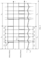
- FIG. 2 is a schematic diagram of waveforms of four drive signals (namely, the first drive signal PWM 1 (dashed line), the second drive signal PWM 2 (dashed line), the third drive signal PWM 3 (solid line), and the fourth drive signal PWM 4 (solid line)).
- i L represents an actual current (solid line) of the inductor L
- I Lavg may represent an average current (dashed line) of the inductor L.
- the first switching transistor S 1 when the first drive signal PWM 1 is at a high level, the first switching transistor S 1 may be turned on, and when the first drive signal PWM 1 is at a low level, the first switching transistor S 1 may be turned off.
- the third switching transistor S 3 when the third drive signal PWM 3 is at a high level, the third switching transistor S 3 may be turned on, and when the third drive signal PWM 3 is at a low level, the third switching transistor S 3 may be turned off.
- the second switching transistor S 2 when the second drive signal PWM 2 is at a high level, the second switching transistor S 2 may be turned on, and when the second drive signal PWM 2 is at a low level, the second switching transistor S 2 may be turned off.
- the second drive signal PWM 2 may be complementary to the fourth drive signal PWM 4 . That is, when the second drive signal PWM 2 is at a high level, the fourth drive signal PWM 4 may be at a low level. Similarly, when the second drive signal PWM 2 is at a low level, the fourth drive signal PWM 4 may be at a high level.
- T delay2 there is also a delay interval (namely, T delay2 in FIG. 2 ) between a falling edge of a first drive pulse of the N drive pulses in the fourth drive signal PWM 4 and a rising edge of a first drive pulse of the N drive pulses in the second drive signal PWM 2 .
- T delay2 a delay interval between a falling edge of a first drive pulse of the N drive pulses in the fourth drive signal PWM 4 and a rising edge of a first drive pulse of the N drive pulses in the second drive signal PWM 2 .
- any cycle of the first switching transistor S 1 there may be a delay between the on moment of the first switching transistor S 1 and the on moment of the second switching transistor S 2 . Therefore, in each cycle of the first drive signal PWM 1 , the rising edge of the first drive pulse of the N drive pulses in the second drive signal PWM 2 may be behind the falling edge of the first drive signal PWM 1 . That is, there is a delay time (namely, a delay) between a first drive pulse of two drive pulses in the second drive signal PWM 2 and the first drive signal PWM 1 .
- a rising edge of the first drive pulse of the N drive pulses in the fourth drive signal PWM 4 may be in front of a falling edge of the third drive signal PWM 3 . That is, there is a delay between a first drive pulse of two drive pulses in the fourth drive signal PWM 4 and the third drive signal PWM 3 .
- the third direct current terminal DC 3 and the fourth direct current terminal DC 4 in FIG. 1 are used as the input terminal of the bidirectional direct current converter, and the first direct current terminal DC 1 and the second direct current terminal DC 2 are used as the output terminal of the bidirectional direct current converter, to describe a control process of the controller for the four switching transistors.
- the bidirectional direct current converter performs reverse working, the bidirectional direct current converter is a buck converter.
- a time period F 11 , a time period F 12 , a time period F 13 , a time period F 14 , a time period F 15 , and a time period F 16 are different time periods of one cycle T sw of the first drive signal PWM 1 .
- the six time periods (namely, the time period F 11 , the time period F 12 , the time period F 13 , the time period F 14 , the time period F 15 , and the time period F 16 ) constitute one cycle T sw of the first drive signal PWM 1 .
- a rising edge of the first drive pulse of the two drive pulses in the second drive signal PWM 2 may be behind the falling edge of the first drive signal PWM 1 . That is, there is a delay time (namely, a delay) between the first drive pulse of the two drive pulses in the second drive signal PWM 2 and the first drive signal PWM 1 .
- the second drive signal PWM 2 may have two drive pulses in each cycle T sw of the first drive signal PWM 1 , and the second drive signal PWM 2 has two drive pulses in low level time periods of each cycle T sw of the first drive signal PWM 1 . Therefore, in one cycle T sw of the first drive signal PWM 1 , the inductor L has three charging and discharging cycles in total, that is, the inductor L completes three times of charging and discharging in one cycle T sw of the first drive signal PWM 1 . This increases the charging and discharging frequency of the inductor L.
- One cycle T sw of the first drive signal PWM 1 may be used as an example.
- the time period F 11 is a high level time period of the first drive signal PWM 1
- the time period F 12 , the time period F 13 , the time period F 14 , the time period F 15 , and the time period F 16 each are a low level time period of the first drive signal PWM 1 .
- the second drive signal PWM 2 has drive pulses in the time period F 13 and the time period F 15 , that is, the second drive signal PWM 2 is at a high level in the time period F 13 and the time period F 15 .
- the second drive signal PWM 2 does not have a drive pulse in the time period F 11 , the time period F 12 , the time period F 14 , and the time period F 16 , that is, the second drive signal PWM 2 is at a low level in the time period F 11 , the time period F 12 , the time period F 14 , and the time period F 16 .
- the second drive signal PWM 2 has two drive pulses in the low level time periods of one cycle T sw of the first drive signal PWM 1 , that is, a drive pulse corresponding to the time period F 13 and a drive pulse corresponding to the time period F 15 . Therefore, the inductor L completes charging and discharging in the time period F 11 and the time period F 12 for the first time, completes charging and discharging in the time period F 13 and the time period F 14 for the second time, and completes charging and discharging in the time period F 15 and the time period F 16 for the third time. It can be learned that the inductor L completes charging and discharging for three times in total. This increases the charging and discharging frequency of the inductor L in one cycle T sw of the first drive signal PWM 1 , and further reduces a ripple current in the inductor L.
- the controller controls the second drive signal PWM 2 to have two drive pulses in the low level time periods of each cycle T sw of the first drive signal PWM 1 to increase the charging and discharging frequency of the inductor L.
- the following uses one cycle T sw of the first drive signal PWM 1 as an example to describe a charging and discharging process of the inductor L.
- the controller may control the first switching transistor S 1 to be turned on and control the second switching transistor S 2 to be turned off, so that the inductor L is discharged, and i L gradually decreases.
- both the first drive signal PWM 1 and the second drive signal PWM 2 are at a low level.
- the controller may control both the first switching transistor S 1 and the second switching transistor S 2 to be turned off, so that the inductor L is charged, and i L gradually increases. In this case, the inductor L completes charging and discharging for the first time.
- the controller may control the first switching transistor S 1 to be turned off and control the second switching transistor S 2 to be turned on, so that the inductor L is discharged, and i L gradually decreases.
- both the first drive signal PWM 1 and the second drive signal PWM 2 are at a low level.
- the controller may control both the first switching transistor S 1 and the second switching transistor S 2 to be turned off, so that the inductor L is charged, and i L gradually increases. In this case, the inductor L completes charging and discharging for the second time.
- the controller may control the first switching transistor S 1 to be turned off and control the second switching transistor S 2 to be turned on, so that the inductor L is discharged, and i L gradually decreases.
- both the first drive signal PWM 1 and the second drive signal PWM 2 are at a low level.
- the controller may control both the first switching transistor S 1 and the second switching transistor S 2 to be turned off, so that the inductor L is charged, and i L gradually increases. In this case, the inductor L completes charging and discharging for the third time.
- the inductor L completes charging and discharging for three times in total in one cycle T sw of the first drive signal PWM 1 .
- the controller sends the first drive signal PWM 1 and the second drive signal PWM 2 that are asymmetric to the first switching transistor S 1 and the second switching transistor S 2 , to increase the quantity of charging and discharging times of the inductor L in each cycle of the first drive signal PWM 1 , that is, increase the charging and discharging frequency of the inductor L. Therefore, the inductor with a small inductance may be used while a same ripple current percentage of the inductor L is ensured. In addition, the inductor with a small inductance has a small size and low costs. This can reduce a size and costs of the bidirectional direct current converter.
- a time period F 21 , a time period F 22 , a time period F 23 , a time period F 24 , a time period F 25 , and a time period F 26 are different time periods of one cycle T sw of the third drive signal PWM 3 .
- the six time periods (namely, the time period F 21 , the time period F 22 , the time period F 23 , the time period F 24 , the time period F 25 , and the time period F 26 ) constitute one cycle T sw of the third drive signal PWM 3 .
- a rising edge of the first drive pulse of the two drive pulses in the fourth drive signal PWM 4 may be in front of the falling edge of the third drive signal PWM 3 . That is, there is also a delay between the first drive pulse of the two drive pulses in the fourth drive signal PWM 4 and the third drive signal PWM 3 .
- the fourth drive signal PWM 4 may have two drive pulses in each cycle T sw of the third drive signal PWM 3 .
- One of the two drive pulses in the fourth drive signal PWM 4 (namely, a first part of drive pulses in a plurality of drive pulses in the fourth drive signal PWM 4 ) is in a low level time period of each cycle T sw of the third drive signal PWM 3
- the other of the two drive pulses in the fourth drive signal PWM 4 (namely, a second part of drive pulses in the plurality of drive pulses in the fourth drive signal PWM 4 ) is in a high level time period of each cycle T sw of the third drive signal PWM 3 .
- the inductor L has three charging and discharging cycles in total, that is, the inductor L completes three times of charging and discharging in one cycle T sw of the third drive signal PWM 3 . Similarly, this can increase the charging and discharging frequency of the inductor L.
- One cycle T sw of the third drive signal PWM 3 may be used as an example.
- the time period F 21 is a low level time period of the third drive signal PWM 3
- the time period F 22 , the time period F 23 , the time period F 24 , the time period F 25 , and the time period F 26 each are a high level time period of the third drive signal PWM 3 .
- the fourth drive signal PWM 4 has drive pulses in the time period F 21 , the time period F 22 , the time period F 24 , and the time period F 26 , that is, the fourth drive signal PWM 4 is at a high level in the time period F 21 , the time period F 22 , the time period F 24 , and the time period F 26 .
- the fourth drive signal PWM 4 does not have a drive pulse in the time period F 23 and the time period F 25 , that is, the fourth drive signal PWM 4 is at a low level in the time period F 23 and the time period F 25 .
- the fourth drive signal PWM 4 has one drive pulse in a low level time period of one cycle T sw of the third drive signal PWM 3 , namely, a drive pulse corresponding to the time period F 21 .
- the fourth drive signal PWM 4 has two drive pulses in high level time periods of one cycle T sw of the third drive signal PWM 3 , namely, a drive pulse corresponding to the time period F 24 and a drive pulse corresponding to the time period F 26 .
- the inductor L completes charging and discharging in the time period F 21 to the time period F 23 for the first time, completes charging and discharging in the time period F 24 and the time period F 26 for the second time, and completes charging and discharging in the time period F 26 for the third time. It can be learned that the inductor L completes charging and discharging for three times in total. This increases the charging and discharging frequency of the inductor L in one cycle T sw of the third drive signal PWM 3 , and further reduces a ripple current in the inductor L.
- the controller controls the fourth drive signal PWM 4 to have one drive pulse in the low level time period and two drive pulses in the high level time periods of each cycle T sw of the third drive signal PWM 3 to increase the charging and discharging frequency of the inductor L.
- the following uses one cycle T sw of the third drive signal PWM 3 as an example to describe a charging and discharging process of the inductor L.
- the controller may control the third switching transistor S 3 to be turned off and control the fourth switching transistor S 4 to be turned on, so that the inductor L is discharged, and i L gradually decreases.
- both the third drive signal PWM 3 and the fourth drive signal PWM 4 are at a high level.
- the controller may control both the third switching transistor S 3 and the fourth switching transistor S 4 to be turned on, so that the inductor L is charged, and i L gradually increases. In this case, the inductor L completes charging and discharging for the first time.
- the controller may control the third switching transistor S 3 to be turned on and control the fourth switching transistor S 4 to be turned off, so that the inductor L is discharged, and i L gradually decreases.
- both the third drive signal PWM 3 and the fourth drive signal PWM 4 are at a high level.
- the controller may control both the third switching transistor S 3 and the fourth switching transistor S 4 to be turned on, so that the inductor L is charged, and i L gradually increases. In this case, the inductor L completes charging and discharging for the second time.
- the controller may control the third switching transistor S 3 to be turned on and control the fourth switching transistor S 4 to be turned off, so that the inductor L is discharged, and i L gradually decreases.
- both the third drive signal PWM 3 and the fourth drive signal PWM 4 are at a high level.
- the controller may control both the third switching transistor S 3 and the fourth switching transistor S 4 to be turned on, so that the inductor L is charged, and i L gradually increases. In this case, the inductor L completes charging and discharging for the third time.
- the inductor L completes charging and discharging for three times in total in one cycle T sw of the third drive signal PWM 3 .
- the controller sends the third drive signal PWM 3 and the fourth drive signal PWM 4 that are asymmetric to the third switching transistor S 3 and the fourth switching transistor S 4 , to increase the quantity of charging and discharging times of the inductor L in each cycle of the third drive signal PWM 3 , that is, increase the charging and discharging frequency of the inductor L. Therefore, the inductor with a small inductance may be used while a same ripple current percentage of the inductor L is ensured. In addition, the inductor with a small inductance has a small size and low costs. This can reduce a size and costs of the bidirectional direct current converter.
- the controller can send the asymmetric drive signals to the first switching transistor and the second switching transistor, and send the asymmetric drive signals to the third switching transistor and the fourth switching transistor.
- This increases the charging and discharging frequency of the inductor, thereby reducing the costs of the inductor, and further reducing the size and the costs of the bidirectional direct current converter.
- power density of the bidirectional direct current converter can be increased.
- the asymmetric drive signals are sent to the first switching transistor and the second switching transistor, and the asymmetric drive signals are sent to the third switching transistor and the fourth switching transistor, so that a state of the first switching transistor is opposite to a state of the third switching transistor (that is, the first switching transistor is complementary to the third switching transistor), and a state of the second switching transistor is opposite to a state of the fourth switching transistor (that is, the second switching transistor is complementary to the fourth switching transistor).
- current sharing or complement is implemented between a branch in which the first switching transistor and the second switching transistor are located and a branch in which the third switching transistor and the fourth switching transistor are located (that is, between two branches), so that a voltage of the capacitor remains stable.
- the bidirectional direct current converter shown in FIG. 1 When the bidirectional direct current converter shown in FIG. 1 performs forward working (to be specific, the first direct current terminal DC 1 and the second direct current terminal DC 2 are used as the input terminal of the bidirectional direct current converter, and the third direct current terminal DC 3 and the fourth direct current terminal DC 4 are used as the output terminal of the bidirectional direct current converter), the bidirectional direct current converter is a boost converter. Therefore, the third switching transistor S 3 and the fourth switching transistor S 4 in the bidirectional direct current converter shown in FIG. 1 may be separately equivalent to a diode. In this case, the controller may send drive signals to only the first switching transistor S 1 and the second switching transistor S 2 .
- FIG. 3 A diagram of waveforms of the first drive signal PWM 1 sent by the controller to the first switching transistor S 1 and the second drive signal PWM 2 sent by the controller to the second switching transistor S 2 is shown in FIG. 3 . It can be seen from FIG. 3 that the first drive signal PWM 1 and the second drive signal PWM 2 are symmetric, that is, cycles of the two drive signals are the same, and duty cycles are also the same.
- the first drive signal PWM 1 may have one drive pulse
- the second drive signal PWM 2 may also have one drive pulse
- the inductor L may perform charging and discharging for two times.
- i L has two cycles. To be specific, when the first drive signal PWM 1 or the second drive signal PWM 2 is at a high level, the inductor L is charged, and i L gradually increases, and when the first drive signal PWM 1 or the second drive signal PWM 2 is at a low level, the inductor L is discharged, and i L gradually decreases.
- the first drive signal PWM 1 and the second drive signal PWM 2 are asymmetric drive signals.
- T sw of the first drive signal PWM 1 the first drive signal PWM 1 has one drive pulse
- the second drive signal PWM 2 has at least two drive pulses
- the inductor L performs charging and discharging for at least three times.
- the asymmetric drive signals can be used to increase a frequency of one (namely, the second drive signal) of the drive signals, thereby increasing the charging and discharging frequency of the inductor L and reducing the inductance of the inductor.
- the bidirectional direct current converter shown in FIG. 1 When the bidirectional direct current converter shown in FIG. 1 performs reverse working (to be specific, the third direct current terminal DC 3 and the fourth direct current terminal DC 4 are used as the input terminal of the bidirectional direct current converter, and the first direct current terminal DC 1 and the second direct current terminal DC 2 are used as the output terminal of the bidirectional direct current converter), the bidirectional direct current converter is a buck converter. Therefore, the first switching transistor S 1 and the second switching transistor S 2 in the bidirectional direct current converter shown in FIG. 1 may be separately equivalent to a diode. In this case, the controller may send drive signals to only the third switching transistor S 3 and the fourth switching transistor S 4 .
- FIG. 4 A diagram of waveforms of the third drive signal PWM 3 sent by the controller to the third switching transistor S 3 and the fourth drive signal PWM 4 sent by the controller to the fourth switching transistor S 4 is shown in FIG. 4 . It can be seen from FIG. 4 that the third drive signal PWM 3 and the fourth drive signal PWM 4 are symmetric, that is, cycles of the two drive signals are the same, and duty cycles are also the same.
- the third drive signal PWM 3 may have one drive pulse
- the fourth drive signal PWM 4 may also have one drive pulse.
- i L has two cycles.
- the inductor L may perform two times of charging and discharging as follows.
- the inductor L When the third drive signal PWM 3 is at a low level and the fourth drive signal PWM 4 is at a high level, the inductor L is charged for the first time and i L gradually increases, when both the third drive signal PWM 3 and the fourth drive signal are at a high level, the inductor L is discharged for the first time and i L gradually decreases, and the inductor L completes charging and discharging for the first time, and when the third drive signal is at a high level and the fourth drive signal PWM 4 is at a low level, the inductor L is charged for the second time and i L gradually increases, when the third drive signal is at a low level and the fourth drive signal PWM 4 is at a low level, the inductor L is discharged for the second time and i L gradually decreases, and the inductor L completes charging and discharging for the second time.
- the asymmetric drive signals can be used to increase a frequency of one (namely, the fourth drive signal) of the drive signals, thereby increasing the charging and discharging frequency of the inductor L and reducing the inductance of the inductor.
- the controller sends the asymmetric drive signals to the first switching transistor S 1 and the second switching transistor S 2 , and sends the asymmetric drive signals to the third switching transistor S 3 and the fourth switching transistor S 4 , to reduce the inductance of the inductor L, thereby reducing the size and the costs of the inductor L, and further reducing the size and the costs of the entire bidirectional direct current converter.
- the first switching transistor S 1 , the second switching transistor S 2 , the third switching transistor S 3 , and the fourth switching transistor S 4 in FIG. 1 may separately use an insulated gate field-effect transistor (or metal-oxide-semiconductor field-effect transistor (MOSFET) or MOS transistor), an insulated-gate bipolar transistor (IGBT), a bidirectional switch, or the like.
- MOSFET metal-oxide-semiconductor field-effect transistor
- IGBT insulated-gate bipolar transistor
- the four switching transistors each may alternatively use another controllable power device. This is not limited in this embodiment of this disclosure.
- the N drive pulses in the second drive signal PWM 2 may exist in each cycle of the first drive signal PWM 1 in the following three manners:
- a quantity of drive pulses that are in the second drive signal PWM 2 and that exist in low level time periods of each cycle of the first drive signal PWM 1 may be not limited, that is, N may be two or more, for example, three or four.
- the N drive pulses in the fourth drive signal PWM 4 may exist in each cycle of the third drive signal PWM 3 in the following three manners:
- a quantity of drive pulses that are in the fourth drive signal PWM 4 and that exist in low level time periods or high level time periods of each cycle of the third drive signal PWM 3 may be not limited.
- the first drive signal PWM 1 is simple, the following describes the second drive signal PWM 2 in one cycle T sw of the first drive signal PWM 1 and the fourth drive signal PWM 4 in one cycle T sw of the third drive signal PWM 3 .
- the second drive signal PWM 2 in one cycle T sw of the first drive signal PWM 1 is first described in the following three aspects:
- frequencies corresponding to at least two of the N drive pulses in the second drive signal PWM 2 are different.
- the following uses an example in which the second drive signal PWM 2 has three drive pulses in low level time periods of each cycle T sw of the first drive signal PWM 1 for description, that is, frequencies corresponding to two of the three drive pulses are different.
- pulse P 1 represents a first drive pulse of the three drive pulses that are in the second drive signal PWM 2 and that are in the low level time periods of each cycle T sw of the first drive signal PWM 1
- P 2 represents a second drive pulse
- P 3 represents a third drive pulse.
- T 1 is a cycle corresponding to the drive pulse P 1
- T 2 is a cycle corresponding to the drive pulse P 2
- T 3 is a cycle corresponding to the drive pulse P 3 .
- both the frequency of the drive pulse P 2 and the frequency of the drive pulse P 3 are different from a frequency of the drive pulse P 1 . It can be seen from FIG. 5 that T 3 >T 1 . Therefore, the frequency corresponding to the drive pulse P 3 is less than the frequency (which may be represented by f 1 ) corresponding to the drive pulse P 1 , that is, f 3 ⁇ f 1 .
- the drive pulse P 0 represents a drive pulse of the first drive signal PWM 1 in one cycle T sw
- the drive pulse P 0 corresponds to an on time of the first switching transistor S 1
- the on time of the first switching transistor S 1 may be obtained by multiplying a duty cycle D 1 of the first switching transistor S 1 by the cycle T sw of the first drive signal PWM 1 .
- the three drive pulses that are in the second drive signal PWM 2 and that exist in the low level time periods of each cycle T sw of the first drive signal PWM 1 may be different.
- pulse widths of a drive pulse P 2 and a drive pulse P 3 are the same, and the pulse widths of the drive pulse P 2 and the drive pulse P 3 are different from a pulse width of a drive pulse P 1 . It can be seen from FIG. 6 that the pulse width of the drive pulse P 1 is greater than the pulse width of the drive pulse P 2 (or the drive pulse P 3 ).
- the charging and discharging frequency of the inductor L is increased. Even if the pulse widths of the drive pulses in the second drive signal PWM 2 are different (as shown in FIG. 6 ), the inductance of the inductor L can still be reduced while a same ripple current percentage of the inductor L is ensured, thereby further reducing the size and the costs of the inductor L.
- a frequency corresponding to each of the N drive pulses in the second drive signal PWM 2 is different.
- a cycle T 3 corresponding to a drive pulse P 3 is greater than a cycle T 2 corresponding to a drive pulse P 2
- the cycle T 2 corresponding to the drive pulse P 2 is greater than a cycle T 1 corresponding to a drive pulse P 1 , that is, T 3 >T 2 >T 1 .
- pulse widths of the three drive pulses that are in the second drive signal PWM 2 and that exist in the low level time periods of each cycle of the first drive signal PWM 1 may alternatively be different.
- a cycle T 3 corresponding to a drive pulse P 3 is greater than a cycle T 2 corresponding to a drive pulse P 2
- the cycle T 2 corresponding to the drive pulse P 2 is greater than a cycle T 1 corresponding to a drive pulse P 1 , that is, T 3 >T 2 >T 1
- a pulse width of the drive pulse P 1 is equal to a pulse width of the drive pulse P 2 .
- both the pulse width of the drive pulse P 1 and the pulse width of the drive pulse P 2 are less than a pulse width of the drive pulse P 3 .
- the second drive signal PWM 2 may have a drive pulse P 1 and a drive pulse P 2 in low level time periods of each cycle of the first drive signal PWM 1 , where a cycle T 2 corresponding to the drive pulse P 2 is greater than a cycle T 1 corresponding to the drive pulse P 1 , that is, T 2 >T 1 .
- a pulse width of the drive pulse P 2 is greater than a pulse width of the drive pulse P 1 (that is, the pulse widths of the drive pulse P 1 and the drive pulse P 2 are different).
- the second drive signal PWM 2 may have two drive pulses in low level time periods of each cycle of the first drive signal PWM 1 , and pulse widths of the two drive pulses are the same, as shown in FIG. 2 . Details are not described in this embodiment of this disclosure again.
- frequencies of first N ⁇ 1 drive pulses of the N drive pulses in the second drive signal PWM 2 are the same, and a frequency of a last drive pulse of the N drive pulses in the second drive signal is less than the frequencies of the first N ⁇ 1 drive pulses.
- the following uses an example in which the second drive signal PWM 2 has three drive pulses in low level time periods of each cycle of the first drive signal PWM 1 for description.
- a cycle of the drive pulse P 3 (namely, a last drive pulse of the three drive pulses) is greater than the cycles of the drive pulse P 1 and the drive pulse P 2 , that is, a frequency of the drive pulse P 3 is less than the frequency of the drive pulse P 1 (or the drive pulse P 2 ) (that is, f 3 ⁇ f 1 ).
- a pulse width of a drive pulse P 1 is greater than a pulse width of a drive pulse P 2
- the pulse width of the drive pulse P 2 is the same as a pulse width of a drive pulse P 3
- a cycle of the drive pulse P 3 is greater than the cycles of the drive pulse P 1 and the drive pulse P 2 , that is, a frequency of the drive pulse P 3 is less than the frequency of the drive pulse P 1 (or the drive pulse P 2 ) (that is, f 3 ⁇ f 1 ).
- the controller sends the asymmetric drive signals to the first switching transistor S 1 and the second switching transistor S 2 , so that the charging and discharging frequency of the inductor L increases, and the inductance of the inductor L can still be reduced while a same ripple current percentage of the inductor L is ensured, thereby further reducing the size and the costs of the inductor L.
- frequencies corresponding to at least two of the N drive pulses in the fourth drive signal PWM 4 are different.
- the following uses an example in which the fourth drive signal PWM 4 has three drive pulses in each cycle T sw of the third drive signal PWM 3 and pulse widths of the three drive pulses are the same for description.
- One drive pulse P 1 exists in a low level time period of each cycle T sw of the third drive signal PWM 3 , two drive pulses (namely, a drive pulse P 2 and a drive pulse P 3 ) exist in high level time periods of each cycle T sw of the third drive signal PWM 3 , and all of a pulse width of the drive pulse P 1 , a pulse width of the drive pulse P 2 , and a pulse width of the drive pulse P 3 are the same.
- the pulse widths of the three drive pulses that are in the fourth drive signal PWM 4 and that exist in each cycle T sw of the third drive signal PWM 3 may alternatively be different.
- the pulse widths of the three drive pulses that are in the fourth drive signal PWM 4 and that exist in each cycle T sw of the third drive signal PWM 3 may alternatively be different.
- the charging and discharging frequency of the inductor L is also increased. Even if the pulse widths of the drive pulses in the fourth drive signal PWM 4 are different, the inductance of the inductor L can still be reduced while a same ripple current percentage of the inductor L is ensured, thereby further reducing the size and the costs of the inductor L.
- a frequency corresponding to each of the N drive pulses in the fourth drive signal PWM 4 is different.
- the fourth drive signal PWM 4 has three drive pulses in each cycle T sw of the third drive signal PWM 3 , pulse widths of the three drive pulses are the same, and all frequencies corresponding to the three drive pulses are different for description.
- One drive pulse P 1 exists in a low level time period of each cycle T sw of the third drive signal PWM 3
- a drive pulse P 2 and a drive pulse P 3 exist in high level time periods of each cycle T sw of the third drive signal PWM 3
- all of a pulse width of the drive pulse P 1 , a pulse width of the drive pulse P 2 , and a pulse width of the drive pulse P 3 are the same.
- the pulse widths of the three drive pulses that are in the fourth drive signal PWM 4 and that exist in each cycle T sw of the third drive signal PWM 3 may alternatively be different.
- the pulse widths of the three drive pulses that are in the fourth drive signal PWM 4 and that exist in each cycle T sw of the third drive signal PWM 3 may alternatively be different.
- frequencies of first N ⁇ 1 drive pulses of the N drive pulses in the fourth drive signal PWM 4 are the same, and a frequency of a last drive pulse of the N drive pulses in the fourth drive signal PWM 4 is less than the frequencies of the first N ⁇ 1 drive pulses.
- the following uses an example in which the fourth drive signal PWM 4 has three drive pulses in low level time periods of each cycle of the third drive signal PWM 3 for description.
- a cycle of the drive pulse P 3 (namely, a last drive pulse of the three drive pulses) is greater than the cycles of the drive pulse P 1 and the drive pulse P 2 , that is, a frequency of the drive pulse P 3 is less than the frequency of the drive pulse P 1 (or the drive pulse P 2 ) (that is, f 3 ⁇ f 1 ).
- a pulse width of a drive pulse P 1 may be greater than a pulse width of a drive pulse P 2 , and the pulse width of the drive pulse P 2 may be the same as a pulse width of a drive pulse P 3 .
- a cycle of the drive pulse P 3 is greater than the cycles of the drive pulse P 1 and the drive pulse P 2 , that is, a frequency of the drive pulse P 3 is less than the frequency of the drive pulse P 1 (or the drive pulse P 2 ) (that is, f 3 ⁇ f 1 ).
- the controller sends the asymmetric drive signals to the third switching transistor S 3 and the fourth switching transistor S 4 , so that the charging and discharging frequency of the inductor L increases, and the inductance of the inductor L can still be reduced while a same ripple current percentage of the inductor L is ensured, thereby further reducing the size and the costs of the inductor L.
- a time between a rising edge of the first drive signal PWM 1 and the rising edge of the first drive pulse of the N drive pulses in the second drive signal PWM 2 may be defined as a lag time (which is the lag time defined in manner 1, and is represented by T d1 for ease of understanding and distinguishing).
- a time between the rising edge of the third drive signal PWM 3 and the rising edge of the first drive pulse of the N drive pulses in the fourth drive signal PWM 4 may be defined as a lag time (which is the lag time defined in manner 2, and is represented by T d2 for ease of understanding and distinguishing).
- the controller may obtain the lag time T d1 based on the ripple current of the inductor L.
- the controller may control a charging current of the inductor L to be equal to a discharging current of the inductor L to obtain the lag time T d1 .
- T sw represents one cycle of the first drive signal PWM 1 .
- D 1 T sw represents the on time of the first switching transistor S 1 .
- D 4 represents a duty cycle of the fourth switching transistor S 4
- D 2 T sw may represent a delay time between the rising edge of the first drive pulse of the two drive pulses in the second drive signal PWM 2 and the falling edge of the first drive signal PWM 1 .
- the controller may obtain the lag time T d1 based on the first voltage V 1 and the second voltage V 2 of the bidirectional direct current converter shown in FIG. 1 , the voltage V c of the capacitor C, and the cycle T sw of the first drive signal PWM 1 or the third drive signal PWM 3 .
- the first voltage V 1 may be used to indicate the output voltage of the bidirectional direct current converter
- the second voltage V 2 may be used to indicate the input voltage of the bidirectional direct current converter
- the first voltage V 1 may be used to indicate the input voltage of the bidirectional direct current converter
- the second voltage V 2 may be used to indicate the output voltage of the bidirectional direct current converter.
- an example in which the first voltage V 1 is the input voltage and the second voltage V 2 is the output voltage is used for description.
- the controller sends the first drive signal PWM 1 to the first switching transistor S 1 and sends the second drive signal PWM 2 to the second switching transistor S 2 .
- the time period F 11 and the time period F 12 correspond to one charging and discharging cycle of the inductor L. Then the time period F 11 corresponds to that the first switching transistor S 1 is turned on and the second switching transistor S 2 is turned off, and the time period F 12 corresponds to that both the first switching transistor S 1 and the second switching transistor S 2 are turned off.
- the controller may obtain the lag time T d1 based on Formula (1) and Formula (2), thereby reducing the inductance of the inductor L.
- the controller may obtain the lag time T d1 based on the loss of at least one of the first switching transistor S 1 and the second switching transistor S 2 (namely, the loss of the first switching transistor S 1 and/or the loss of the second switching transistor S 1 ).
- the controller may obtain the lag time T d1 based on only the loss of the first switching transistor S 1 , may obtain the lag time T d1 based on only the loss of the second switching transistor S 2 , or may obtain the lag time T d1 based on both the loss of the first switching transistor S 1 and the loss of the second switching transistor S 2 .
- the controller obtains the lag time T d1 based on only the loss of the first switching transistor S 1 .
- a time corresponding to a minimum loss of the first switching transistor S 1 may be the lag time T d1 .
- the controller obtains the lag time T d1 based on only the loss of the second switching transistor S 2 .
- a time corresponding to a minimum loss of the second switching transistor S 2 may be the lag time T d1 .
- the controller obtains the lag time T d1 based on both the loss of the first switching transistor S 1 and the loss of the second switching transistor S 2 .
- a time corresponding to evenly distributed losses of the first switching transistor S 1 and the second switching transistor S 2 may be the lag time T d1 .
- the controller may obtain the lag time T d1 based on the loss of the first switching transistor S 1 and/or the loss of the second switching transistor S 1 , thereby reducing a loss generated by the bidirectional direct current converter and improving conversion efficiency of the bidirectional direct current converter.
- the controller may obtain the lag time T d1 based on the ripple current of the inductor L and the loss of at least one of the first switching transistor S 1 and the second switching transistor S 2 .
- the controller may obtain the lag time T d1 by combining the first example and the second example.
- the controller can use a time corresponding to a low ripple current of the inductor L and a low loss of at least one of the first switching transistor S 1 and the second switching transistor S 2 as the lag time T d1 .
- the controller may obtain the lag time T d2 based on the ripple current of the inductor L.
- the controller may control a charging current of the inductor L to be equal to a discharging current of the inductor L to obtain the lag time T d2 .
- the controller may obtain the lag time T d2 based on the loss of at least one of the third switching transistor S 3 and the fourth switching transistor S 4 (namely, the loss of the third switching transistor S 3 and/or the loss of the fourth switching transistor S 4 ).
- the controller may obtain the lag time T d2 based on only the loss of the third switching transistor S 3 , may obtain the lag time T d2 based on only the loss of the fourth switching transistor S 4 , or may obtain the lag time T d2 based on both the loss of the third switching transistor S 3 and the loss of the fourth switching transistor S 4 .
- the controller obtains the lag time T d2 based on only the loss of the third switching transistor S 3 .
- a time corresponding to a minimum loss of the third switching transistor S 3 may be the lag time T d2 .
- the controller obtains the lag time T d2 based on only the loss of the fourth switching transistor S 4 .
- a time corresponding to a minimum loss of the fourth switching transistor S 4 may be the lag time T d2 .
- the controller obtains the lag time T d2 based on both the loss of the third switching transistor S 3 and the loss of the fourth switching transistor S 4 .
- a time corresponding to evenly distributed losses of the third switching transistor S 3 and the fourth switching transistor S 4 may be the lag time T d2 .
- the controller may obtain the lag time T d2 based on the loss of the third switching transistor S 3 and/or the loss of the fourth switching transistor S 4 , thereby reducing a loss generated by the bidirectional direct current converter and improving conversion efficiency of the bidirectional direct current converter.
- the controller may obtain the lag time T 2 based on the ripple current of the inductor L and the loss of at least one of the third switching transistor S 3 and the fourth switching transistor S 4 .
- the controller may obtain the lag time T d2 by combining the first example and the second example.
- the controller can use a time corresponding to a low ripple current of the inductor L and a low loss of at least one of the third switching transistor S 3 and the fourth switching transistor S 4 as the lag time T d2 .
- the bidirectional direct current converter 1 provided in this embodiment of this disclosure may further include a capacitor C 1 and a capacitor C 2 , as shown in FIG. 13 .
- the capacitor C 1 is connected between a node H and a node I, the node H is connected to the first direct current terminal DC 1 , and the node I is connected to the second direct current terminal DC 2 .
- the capacitor C 2 is connected between a node F and a node G, the node F is connected to the third direct current terminal DC 3 , and the node G is connected to the fourth direct current terminal DC 4 .
- one terminal (which may be a positive terminal) of the capacitor C 1 is connected to the node H, and the other terminal (which may be a negative terminal) of the capacitor C 1 is connected to the node I.
- One terminal (which may be a positive terminal) of the capacitor C 2 is connected to the node F, and the other terminal (which may be a negative terminal) of the capacitor C 2 is connected to the node G.
- the bidirectional direct current converter 1 provided in this embodiment of this disclosure may further include a fifth switching transistor S 5 , as shown in FIG. 14 .
- a first terminal (namely, a right terminal of the fifth switching transistor S 5 in FIG. 14 ) of the fifth switching transistor S 5 is connected to the second terminal of the capacitor C (namely, a lower terminal of the capacitor C in FIG. 14 , which may be a negative terminal), and a second terminal (namely, a left terminal of the fifth switching transistor S 5 in FIG. 14 ) of the fifth switching transistor S 5 may be connected to the node B.
- the fifth switching transistor S 5 may also use a MOS transistor, an IGBT, a bidirectional switch, or the like. Certainly, the fifth switching transistor S 5 may alternatively be another type of controllable power device. A type of the fifth switching transistor S 5 is not limited in this embodiment of this disclosure.
- the fifth switching transistor S 5 is a MOS transistor.
- a drain of the fifth switching transistor S 5 may be connected to the second terminal of the capacitor C, and a source of the fifth switching transistor S 5 may be connected to the node B.
- the fifth switching transistor S 5 is an IGBT.
- a collector of the fifth switching transistor S 5 may be connected to the second terminal of the capacitor C, and an emitter of the fifth switching transistor S 5 may be connected to the node B.
- the bidirectional direct current converter 1 shown in FIG. 14 may protect the second switching transistor S 2 by using the fifth switching transistor S 5 .
- a principle is as follows.
- the controller may first control the fifth switching transistor S 5 to be turned off. In this case, a current cannot flow through the capacitor C because the fifth switching transistor S 5 is turned off. In this case, the first voltage V 1 is not applied to the second switching transistor S 2 . Therefore, the second switching transistor S 2 is protected.
- the first switching transistor S 1 and the third switching transistor S 3 each may use an IGBT with a low withstand voltage level, for example, 650 V. If the fifth switching transistor S 5 is not disposed, the voltage V c on the capacitor C is 0 at a moment when the bidirectional direct current converter 1 is connected to a power supply, that is, the first voltage V 1 is almost completely applied to the second switching transistor S 2 . Consequently, the voltage that needs to be borne by the second switching transistor S 2 exceeds voltage stress of the second switching transistor S 2 , and the second switching transistor S 2 is damaged.
- the controller may first control the fifth switching transistor S 5 to be turned off. In this case, a current cannot flow through the capacitor C because the fifth switching transistor S 5 is turned off. In this case, the second voltage V 2 is not applied to the second switching transistor S 2 . Therefore, the second switching transistor S 2 may be still protected.
- the first switching transistor S 1 and the third switching transistor S 3 each may use an IGBT with a low withstand voltage level, for example, 650 V. If the fifth switching transistor S 5 is not disposed, the voltage V c on the capacitor C is 0 at a moment when the bidirectional direct current converter 1 is connected to a power supply, that is, the second voltage V 2 is almost completely applied to the second switching transistor S 2 . Consequently, the voltage that needs to be borne by the second switching transistor S 2 exceeds voltage stress of the second switching transistor S 2 , and the second switching transistor S 2 is damaged.
- the bidirectional direct current converter 1 may further include a first diode D 1 and a second diode D 2 , as shown in FIG. 15 .
- the second capacitor C 2 in FIG. 13 may be divided into a capacitor C 21 and a capacitor C 22 , and a connection node between the capacitor C 21 and the capacitor C 22 is a node J (the node J may be understood as a midpoint of the second voltage V 2 ).
- An anode of the first diode D 1 may be connected to a node B, and a cathode of the first diode D 1 may be connected to the node J.
- An anode of the second diode D 2 may be connected to the node J, and a cathode of the second diode D 2 may be connected to the node D.
- a function of the first diode D 1 is to clamp a voltage drop borne by the second switching transistor S 2 , to prevent the second switching transistor S 2 from bearing a voltage V bus (namely, the second voltage V 2 ) of an entire direct current bus when the fourth switching transistor S 4 is turned on.
- a function of the second diode D 2 is to clamp a voltage drop borne by the fourth switching transistor S 4 , to prevent the fourth switching transistor S 4 from bearing a voltage V bus (namely, the second voltage V 2 ) of an entire direct current bus when the second switching transistor S 2 is turned on. Therefore, the first diode D 1 and the second diode D 2 may be referred to as clamping diodes.
- a function of the bidirectional direct current converter 1 shown in FIG. 15 is the same as that of the bidirectional direct current converter 1 shown in FIG. 14 . Both the functions are reducing the voltage stress borne by the second switching transistor S 2 when the bidirectional direct current converter 1 is connected to the power supply and starts to work.
- the bidirectional direct current converter shown in FIG. 15 has the following advantages.
- the capacitor C When the bidirectional direct current converter 1 is connected to the power supply and starts to perform forward working, the capacitor C is charged by using the first voltage V 1 , and there is no moment at which the voltage of the capacitor C is zero. Therefore, the first voltage V 1 is not completely applied to the second switching transistor S 2 , thereby reducing the voltage stress borne by the second switching transistor S 2 , and protecting the second switching transistor S 2 .
- the capacitor C is charged by using the second voltage V 2 , and there is no moment at which the voltage of the capacitor C is zero either. Therefore, the second voltage V 2 is not completely applied to the second switching transistor S 2 , thereby reducing the voltage stress borne by the second switching transistor S 2 , and protecting the second switching transistor.
- the first diode and the second diode each may alternatively be replaced with a switching transistor (for example, a MOS transistor, an IGBT, or a bidirectional switch).
- a switching transistor for example, a MOS transistor, an IGBT, or a bidirectional switch.
- the controller only needs to send corresponding drive signals, so that the switching transistors implement working modes of the diodes. Details are not described in this embodiment of this disclosure again.
- the controller may also send the asymmetric drive signals to the first switching transistor S 1 and the second switching transistor S 2 , and send the asymmetric drive signals to the third switching transistor S 3 and the fourth switching transistor S 4 .
- This can also increase the charging and discharging frequency of the inductor L, reduce the ripple current of the inductor L, reduce the inductance of the inductor L, and reduce the size and the costs of the entire bidirectional direct current converter.
- An embodiment of this disclosure further provides an electronic device.
- the electronic device may include a bidirectional direct current converter.
- the bidirectional direct current converter refer to the foregoing descriptions. Details are not described in this embodiment of this disclosure again.
- the control method 100 may include the following.
- a controller performs complementary control on a first switching transistor S 1 and a third switching transistor S 3 , and performs complementary control on a second switching transistor S 2 and a fourth switching transistor S 4 .
- the complementary control is used to indicate that two switching transistors in complementary control cannot be simultaneously turned on or off.
- the first switching transistor S 1 and the third switching transistor S 3 cannot be simultaneously turned on or off
- the second switching transistor S 2 and the fourth switching transistor S 4 cannot be simultaneously turned on or off.
- the controller controls a quantity of on times of the second switching transistor S 2 to be greater than a quantity of on times of the first switching transistor S 1 in a same cycle. It may also be understood as that, in one cycle, the controller may control a switching frequency of the second switching transistor S 2 to be greater than a switching frequency of the first switching transistor S 1 , thereby reducing losses of the first switching transistor S 1 and the second switching transistor S 2 .
- the controller controls the quantity of on times of the second switching transistor to be different from the quantity of on times of the first switching transistor in a same cycle.
- This can increase a quantity of charging and discharging times of the inductor in one cycle, that is, increase a charging and discharging frequency of the inductor. Therefore, the inductor with a small inductance may be used while a same ripple current percentage of the inductor is ensured.
- the inductor with a small inductance has a small size and low costs. This can reduce a size and costs of the bidirectional direct current converter. When the size of the bidirectional direct current converter is reduced, power density of the bidirectional direct current converter can be increased.
- any cycle of the first switching transistor S 1 there may be a delay between an on moment of the first switching transistor S 1 and an on moment of the second switching transistor S 2 . That is, the first switching transistor S 1 and the second switching transistor S 2 are not simultaneously turned on in any cycle.
- a cycle of the first switching transistor S 1 may be the same as a cycle of the third switching transistor S 3 .
- control method may further include the following.
- the controller controls a quantity of on times of the fourth switching transistor S 4 to be greater than a quantity of on times of the third switching transistor S 3 in a same cycle. It may also be understood as that, in one cycle, the controller may control a switching frequency of the fourth switching transistor S 4 to be greater than a switching frequency of the third switching transistor S 3 , thereby reducing losses of the third switching transistor S 3 and the fourth switching transistor S 4 .
- the controller controls the quantity of on times of the fourth switching transistor to be different from the quantity of on times of the third switching transistor in a same cycle. Similarly, this can increase a quantity of charging and discharging times of the inductor in one cycle, that is, increase a charging and discharging frequency of the inductor. Therefore, the inductor with a small inductance may be used while a same ripple current percentage of the inductor is ensured. In addition, the inductor with a small inductance has a small size and low costs. This can reduce a size and costs of the bidirectional direct current converter. When the size of the bidirectional direct current converter is reduced, power density of the bidirectional direct current converter can be increased.
- the controller may send a first drive signal PWM 1 to the first switching transistor S 1 , send a second drive signal PWM 2 to the second switching transistor S 2 , send a third drive signal PWM 3 to the third switching transistor S 3 , and send a fourth drive signal PWM 4 to the fourth switching transistor S 4 , to implement complementary control on the first switching transistor S 1 and the third switching transistor S 3 , and implement complementary control on the second switching transistor S 2 and the fourth switching transistor S 4 .
- the cycle of the first switching transistor S 1 may be the same as the cycle of the third switching transistor S 3 . Therefore, a cycle of the first drive signal may be the same as a cycle of the third drive signal.
- the second drive signal may have N drive pulses in each cycle of the first drive signal, that is, the second drive signal and the first drive signal are two asymmetric drive signals.
- the fourth drive signal may also have N drive pulses in each cycle of the third drive signal, that is, the fourth drive signal and the third drive signal are two asymmetric drive signals.
- An inductor in the bidirectional direct current converter has N+1 charging and discharging cycles in each cycle of the first drive signal or the third drive signal, where N may be an integer greater than or equal to 2.
- N may be an integer greater than or equal to 2.
- a value of N is not limited in this embodiment of this disclosure.
- the inductor L may perform charging and discharging for at least two times by sending the second drive signal PWM 2 to the second switching transistor S 2 .
- the inductor L may alternatively perform charging and discharging for one time by sending the first drive signal PWM 1 to the first switching transistor S 1 .
- the inductor L may perform charging and discharging for at least two times by sending the fourth drive signal PWM 4 to the fourth switching transistor S 4 .
- the inductor L may alternatively perform charging and discharging for one time by sending the third drive signal PWM 3 to the third switching transistor S 3 .
- the inductor L has at least three charging and discharging cycles.
- the controller increases a charging and discharging frequency of the inductor L in each cycle (namely, frequency increase), thereby reducing an inductance of the inductor L, and reducing a size and costs of the inductor L.
Landscapes
- Engineering & Computer Science (AREA)
- Power Engineering (AREA)
- Dc-Dc Converters (AREA)
Abstract
Description
(V 1 +V c −V 2)D 1 T sw=(V 2 −V 1)D 2 T sw
-
- Manner 1: All the N drive pulses in the second drive signal PWM2 may be in low level time periods of each cycle of the first drive signal PWM1.
- Manner 2: All the N drive pulses in the second drive signal PWM2 may be in high level time periods of each cycle of the first drive signal PWM1.
- Manner 3: The N drive pulses in the second drive signal PWM2 may be divided into a first part of drive pulses and a second part of drive pulses. The first part of drive pulses may be in low level time periods of each cycle of the first drive signal PWM1, and the second part of drive pulses may be in high level time periods of each cycle of the first drive signal PWM1.
-
- Manner 1: All the N drive pulses in the fourth drive signal PWM4 may be in low level time periods of each cycle of the third drive signal PWM3.
- Manner 2: All the N drive pulses in the fourth drive signal PWM4 may be in high level time periods of each cycle of the third drive signal PWM3.
- Manner 3: The N drive pulses in the fourth drive signal may be divided into a first part of drive pulses and a second part of drive pulses. The first part of drive pulses may be in low level time periods of each cycle of the third drive signal PWM3, and the second part of drive pulses may be in high level time periods of each cycle of the third drive signal PWM3.
(V 1 +V c −V 2)D 1 T sw=(V 2 −V 1)D 2 T sw Formula(1)
D 1=1−V 1 /V 2 Formula (2)
Claims (20)
(V 1 +V c −V 2)D 1 T sw=(V 2 −V 1)D 2 T sw,
Applications Claiming Priority (2)
| Application Number | Priority Date | Filing Date | Title |
|---|---|---|---|
| CN202111489706.5A CN114285277B (en) | 2021-12-08 | 2021-12-08 | Bidirectional DC converter and control method thereof |
| CN202111489706.5 | 2021-12-08 |
Publications (2)
| Publication Number | Publication Date |
|---|---|
| US20230179106A1 US20230179106A1 (en) | 2023-06-08 |
| US12328071B2 true US12328071B2 (en) | 2025-06-10 |
Family
ID=80871191
Family Applications (1)
| Application Number | Title | Priority Date | Filing Date |
|---|---|---|---|
| US18/063,321 Active 2043-09-21 US12328071B2 (en) | 2021-12-08 | 2022-12-08 | Bidirectional direct current converter and control method thereof |
Country Status (4)
| Country | Link |
|---|---|
| US (1) | US12328071B2 (en) |
| EP (1) | EP4195484A1 (en) |
| JP (1) | JP2023085241A (en) |
| CN (1) | CN114285277B (en) |
Citations (17)
| Publication number | Priority date | Publication date | Assignee | Title |
|---|---|---|---|---|
| WO2012074967A1 (en) | 2010-11-29 | 2012-06-07 | President And Fellows Of Harvard College | Fully integrated 3-level dc/dc converter for nanosecond-scale dynamic voltage scaling with fast shunt regulation |
| US20140266135A1 (en) * | 2013-03-15 | 2014-09-18 | Maxim Integrated Products, Inc. | Multi-level step-up converter topologies, control and soft start systems and methods |
| JP2014192983A (en) | 2013-03-26 | 2014-10-06 | Mitsubishi Heavy Ind Ltd | Switching power-supply circuit |
| CN104901538A (en) | 2015-05-29 | 2015-09-09 | 重庆大学 | Second-order sliding mode controller and flying capacitor voltage balance method of three-level DC-DC buck converter |
| US20160190921A1 (en) | 2014-12-24 | 2016-06-30 | Intel Corporation | Selectable-mode voltage regulator topology |
| WO2016125682A1 (en) | 2015-02-03 | 2016-08-11 | 三菱電機株式会社 | Dc/dc converter |
| EP3242385A1 (en) | 2016-05-06 | 2017-11-08 | Merus Audio ApS | A load adaptable boost dc-dc power converter |
| US20170373586A1 (en) | 2016-06-24 | 2017-12-28 | General Electric Company | Modulator for a hybrid converter system |
| US20180026518A1 (en) | 2016-07-07 | 2018-01-25 | Tianshu Liu | Multi-Stage Multilevel DC-DC Step-Down Converter |
| US20180034364A1 (en) * | 2016-07-29 | 2018-02-01 | Mitsubishi Electric Corporation | Dc/dc converter |
| US20180183333A1 (en) * | 2015-09-16 | 2018-06-28 | Mitsubishi Electric Corporation | Electric power converter and driving apparatus |
| CN111200309A (en) | 2020-01-13 | 2020-05-26 | 深圳市高斯宝电气技术有限公司 | Bidirectional direct-current charger circuit |
| WO2020112207A2 (en) | 2019-09-11 | 2020-06-04 | Futurewei Technologies, Inc. | Switched-capacitor power conversion system and control method |
| CN210867509U (en) | 2019-11-04 | 2020-06-26 | 河北电立方新能源科技有限公司 | Bidirectional DC/DC Converters and Systems |
| EP3709497A1 (en) | 2019-03-14 | 2020-09-16 | ABB Schweiz AG | Cascaded pulse width modulation converter control |
| EP3846329A1 (en) | 2019-12-31 | 2021-07-07 | Solaredge Technologies Ltd. | Dc balancer circuit with zvs |
| WO2022016891A1 (en) | 2020-07-22 | 2022-01-27 | 华为数字能源技术有限公司 | Three-level boost converter and control method |
-
2021
- 2021-12-08 CN CN202111489706.5A patent/CN114285277B/en active Active
-
2022
- 2022-12-07 JP JP2022195904A patent/JP2023085241A/en active Pending
- 2022-12-08 US US18/063,321 patent/US12328071B2/en active Active
- 2022-12-08 EP EP22212361.4A patent/EP4195484A1/en active Pending
Patent Citations (19)
| Publication number | Priority date | Publication date | Assignee | Title |
|---|---|---|---|---|
| WO2012074967A1 (en) | 2010-11-29 | 2012-06-07 | President And Fellows Of Harvard College | Fully integrated 3-level dc/dc converter for nanosecond-scale dynamic voltage scaling with fast shunt regulation |
| US20140266135A1 (en) * | 2013-03-15 | 2014-09-18 | Maxim Integrated Products, Inc. | Multi-level step-up converter topologies, control and soft start systems and methods |
| JP2014192983A (en) | 2013-03-26 | 2014-10-06 | Mitsubishi Heavy Ind Ltd | Switching power-supply circuit |
| US20160190921A1 (en) | 2014-12-24 | 2016-06-30 | Intel Corporation | Selectable-mode voltage regulator topology |
| WO2016125682A1 (en) | 2015-02-03 | 2016-08-11 | 三菱電機株式会社 | Dc/dc converter |
| US20170250617A1 (en) | 2015-02-03 | 2017-08-31 | Mitsubishi Electric Corporation | Dc/dc converter |
| CN104901538A (en) | 2015-05-29 | 2015-09-09 | 重庆大学 | Second-order sliding mode controller and flying capacitor voltage balance method of three-level DC-DC buck converter |
| US20180183333A1 (en) * | 2015-09-16 | 2018-06-28 | Mitsubishi Electric Corporation | Electric power converter and driving apparatus |
| US20170324321A1 (en) * | 2016-05-06 | 2017-11-09 | Merus Audio Aps | Load adaptable boost dc-dc power converter |
| EP3242385A1 (en) | 2016-05-06 | 2017-11-08 | Merus Audio ApS | A load adaptable boost dc-dc power converter |
| US20170373586A1 (en) | 2016-06-24 | 2017-12-28 | General Electric Company | Modulator for a hybrid converter system |
| US20180026518A1 (en) | 2016-07-07 | 2018-01-25 | Tianshu Liu | Multi-Stage Multilevel DC-DC Step-Down Converter |
| US20180034364A1 (en) * | 2016-07-29 | 2018-02-01 | Mitsubishi Electric Corporation | Dc/dc converter |
| EP3709497A1 (en) | 2019-03-14 | 2020-09-16 | ABB Schweiz AG | Cascaded pulse width modulation converter control |
| WO2020112207A2 (en) | 2019-09-11 | 2020-06-04 | Futurewei Technologies, Inc. | Switched-capacitor power conversion system and control method |
| CN210867509U (en) | 2019-11-04 | 2020-06-26 | 河北电立方新能源科技有限公司 | Bidirectional DC/DC Converters and Systems |
| EP3846329A1 (en) | 2019-12-31 | 2021-07-07 | Solaredge Technologies Ltd. | Dc balancer circuit with zvs |
| CN111200309A (en) | 2020-01-13 | 2020-05-26 | 深圳市高斯宝电气技术有限公司 | Bidirectional direct-current charger circuit |
| WO2022016891A1 (en) | 2020-07-22 | 2022-01-27 | 华为数字能源技术有限公司 | Three-level boost converter and control method |
Non-Patent Citations (3)
| Title |
|---|
| Chen Siyuan et al: "Bidirectional H8 AC-DC Topology Combining Advantages of Both Diode-Clamped and Flying-Capacitor Three-Level Converters",IEEE Journal of Emerging and Selected Topics in Power Electronics, IEEE, Piscataway, NJ, USA, vol. 10, No. 4, Jun. 10, 2021 (Jun. 10, 2021), pp. 3643-3651, XP011916814. |
| Handong Gui, et al., "Modeling and Mitigation of Multiloops Related Device Overvoltage in Three-Level Active Neutral Point Clamped Converter," IEEE Transactions on Power Electronics, Dec. 27, 2019, 13 pages. |
| Miroslav Vasi, et al., "Ultraefficient Voltage Doubler Based on a GaN Resonant Switched-Capacitor Converter," IEEE Journal of Emerging and Selected Topics in Power Electronics, vol. 7, No. 2, Jun. 2019, 14 pages. |
Also Published As
| Publication number | Publication date |
|---|---|
| JP2023085241A (en) | 2023-06-20 |
| CN114285277B (en) | 2024-03-26 |
| EP4195484A1 (en) | 2023-06-14 |
| US20230179106A1 (en) | 2023-06-08 |
| CN114285277A (en) | 2022-04-05 |
Similar Documents
| Publication | Publication Date | Title |
|---|---|---|
| US8422179B2 (en) | Inrush current control | |
| US9007040B2 (en) | DC-DC power conversion apparatus | |
| US6411535B1 (en) | Power factor correction circuit with integral bridge function | |
| US20060274558A1 (en) | Snubber circuit for a power converter | |
| US20150381031A1 (en) | Flyback converter | |
| US11239746B2 (en) | Two-stage converter and method for starting the same, LLC converter, and application system | |
| JP6706811B2 (en) | Snubber circuit and power conversion system using the same | |
| KR20090024800A (en) | High efficiency power converter system | |
| EP2698911A1 (en) | Power electronic circuit | |
| US12483128B2 (en) | Three-level boost converter and control method | |
| US20250167681A1 (en) | Power conversion apparatus, control method, and power supply system | |
| US12580493B2 (en) | Neutral point clamped inverter and photovoltaic power supply system | |
| US20230299680A1 (en) | Power Supply and Current Sampling Method | |
| EP2398135A2 (en) | DC/DC power converter having active self driving synchronous rectification | |
| Moradzadeh et al. | Novel high step-up DC/DC converter structure using a coupled inductor with minimal voltage stress on the main switch | |
| US12328071B2 (en) | Bidirectional direct current converter and control method thereof | |
| Anthony et al. | The efficient deployment of silicon super-junction MOSFETs as synchronous rectifiers | |
| CN218771782U (en) | DC converter and grid-connected inverter | |
| CN109586560A (en) | The control circuit controlled for the dead time to DC-to-dc converter | |
| Kumar et al. | A PV-connected soft-switched synchronous Buck Converter for Electrical Vehicle | |
| CN218162219U (en) | Load management circuit and load management system | |
| CN218514286U (en) | Charging circuit and three-phase grid-connected inverter | |
| US20260066771A1 (en) | Drive Circuit | |
| US20250392157A1 (en) | Power converters and unnterruptible power supplies (upss) including the same | |
| US20250253773A1 (en) | Power converter and control method |
Legal Events
| Date | Code | Title | Description |
|---|---|---|---|
| FEPP | Fee payment procedure |
Free format text: ENTITY STATUS SET TO UNDISCOUNTED (ORIGINAL EVENT CODE: BIG.); ENTITY STATUS OF PATENT OWNER: LARGE ENTITY |
|
| STPP | Information on status: patent application and granting procedure in general |
Free format text: DOCKETED NEW CASE - READY FOR EXAMINATION |
|
| AS | Assignment |
Owner name: HUAWEI DIGITAL POWER TECHNOLOGIES CO., LTD., CHINA Free format text: ASSIGNMENT OF ASSIGNORS INTEREST;ASSIGNORS:WANG, JUN;SHI, LEI;LIU, YUNFENG;AND OTHERS;SIGNING DATES FROM 20230209 TO 20240828;REEL/FRAME:068423/0578 |
|
| STPP | Information on status: patent application and granting procedure in general |
Free format text: NON FINAL ACTION MAILED |
|
| STPP | Information on status: patent application and granting procedure in general |
Free format text: RESPONSE TO NON-FINAL OFFICE ACTION ENTERED AND FORWARDED TO EXAMINER |
|
| STPP | Information on status: patent application and granting procedure in general |
Free format text: NOTICE OF ALLOWANCE MAILED -- APPLICATION RECEIVED IN OFFICE OF PUBLICATIONS |
|
| STCF | Information on status: patent grant |
Free format text: PATENTED CASE |
|
| CC | Certificate of correction |