US12320971B2 - Optical scanning device, driving method of optical scanning device, and image drawing system - Google Patents
Optical scanning device, driving method of optical scanning device, and image drawing system Download PDFInfo
- Publication number
- US12320971B2 US12320971B2 US17/738,515 US202217738515A US12320971B2 US 12320971 B2 US12320971 B2 US 12320971B2 US 202217738515 A US202217738515 A US 202217738515A US 12320971 B2 US12320971 B2 US 12320971B2
- Authority
- US
- United States
- Prior art keywords
- driving
- angle
- axis
- signal
- frequency
- Prior art date
- Legal status (The legal status is an assumption and is not a legal conclusion. Google has not performed a legal analysis and makes no representation as to the accuracy of the status listed.)
- Active, expires
Links
Images


Classifications
-
- G—PHYSICS
- G02—OPTICS
- G02B—OPTICAL ELEMENTS, SYSTEMS OR APPARATUS
- G02B26/00—Optical devices or arrangements for the control of light using movable or deformable optical elements
- G02B26/08—Optical devices or arrangements for the control of light using movable or deformable optical elements for controlling the direction of light
- G02B26/10—Scanning systems
- G02B26/105—Scanning systems with one or more pivoting mirrors or galvano-mirrors
-
- G—PHYSICS
- G02—OPTICS
- G02B—OPTICAL ELEMENTS, SYSTEMS OR APPARATUS
- G02B26/00—Optical devices or arrangements for the control of light using movable or deformable optical elements
- G02B26/08—Optical devices or arrangements for the control of light using movable or deformable optical elements for controlling the direction of light
- G02B26/10—Scanning systems
- G02B26/101—Scanning systems with both horizontal and vertical deflecting means, e.g. raster or XY scanners
-
- G—PHYSICS
- G01—MEASURING; TESTING
- G01L—MEASURING FORCE, STRESS, TORQUE, WORK, MECHANICAL POWER, MECHANICAL EFFICIENCY, OR FLUID PRESSURE
- G01L1/00—Measuring force or stress, in general
- G01L1/16—Measuring force or stress, in general using properties of piezoelectric devices
-
- G—PHYSICS
- G02—OPTICS
- G02B—OPTICAL ELEMENTS, SYSTEMS OR APPARATUS
- G02B26/00—Optical devices or arrangements for the control of light using movable or deformable optical elements
- G02B26/08—Optical devices or arrangements for the control of light using movable or deformable optical elements for controlling the direction of light
- G02B26/0816—Optical devices or arrangements for the control of light using movable or deformable optical elements for controlling the direction of light by means of one or more reflecting elements
- G02B26/0833—Optical devices or arrangements for the control of light using movable or deformable optical elements for controlling the direction of light by means of one or more reflecting elements the reflecting element being a micromechanical device, e.g. a MEMS mirror, DMD
- G02B26/0858—Optical devices or arrangements for the control of light using movable or deformable optical elements for controlling the direction of light by means of one or more reflecting elements the reflecting element being a micromechanical device, e.g. a MEMS mirror, DMD the reflecting means being moved or deformed by piezoelectric means
-
- G—PHYSICS
- G02—OPTICS
- G02B—OPTICAL ELEMENTS, SYSTEMS OR APPARATUS
- G02B26/00—Optical devices or arrangements for the control of light using movable or deformable optical elements
- G02B26/08—Optical devices or arrangements for the control of light using movable or deformable optical elements for controlling the direction of light
- G02B26/10—Scanning systems
-
- H—ELECTRICITY
- H02—GENERATION; CONVERSION OR DISTRIBUTION OF ELECTRIC POWER
- H02K—DYNAMO-ELECTRIC MACHINES
- H02K1/00—Details of the magnetic circuit
- H02K1/06—Details of the magnetic circuit characterised by the shape, form or construction
- H02K1/12—Stationary parts of the magnetic circuit
-
- H—ELECTRICITY
- H02—GENERATION; CONVERSION OR DISTRIBUTION OF ELECTRIC POWER
- H02K—DYNAMO-ELECTRIC MACHINES
- H02K1/00—Details of the magnetic circuit
- H02K1/06—Details of the magnetic circuit characterised by the shape, form or construction
- H02K1/34—Reciprocating, oscillating or vibrating parts of the magnetic circuit
-
- H—ELECTRICITY
- H04—ELECTRIC COMMUNICATION TECHNIQUE
- H04N—PICTORIAL COMMUNICATION, e.g. TELEVISION
- H04N9/00—Details of colour television systems
- H04N9/12—Picture reproducers
- H04N9/31—Projection devices for colour picture display, e.g. using electronic spatial light modulators [ESLM]
- H04N9/3129—Projection devices for colour picture display, e.g. using electronic spatial light modulators [ESLM] scanning a light beam on the display screen
- H04N9/3135—Driving therefor
-
- H—ELECTRICITY
- H04—ELECTRIC COMMUNICATION TECHNIQUE
- H04N—PICTORIAL COMMUNICATION, e.g. TELEVISION
- H04N9/00—Details of colour television systems
- H04N9/12—Picture reproducers
- H04N9/31—Projection devices for colour picture display, e.g. using electronic spatial light modulators [ESLM]
- H04N9/3191—Testing thereof
- H04N9/3194—Testing thereof including sensor feedback
Definitions
- the present disclosure relates to an optical scanning device, a driving method of an optical scanning device, and an image drawing system.
- a micromirror device (also referred to as a microscanner) is known as one of micro electro mechanical systems (MEMS) devices manufactured using the silicon (Si) microfabrication technique.
- MEMS micro electro mechanical systems
- An optical scanning device comprising the micromirror device is small and has low power consumption. Thus, applications in image drawing systems such as laser displays or laser projectors are expected.
- a mirror portion is formed to be capable of swinging around a first axis and a second axis that are orthogonal to each other, and light reflected by the mirror portion is two-dimensionally scanned by the swing of the mirror portion around each axis.
- a micromirror device that enables Lissajous scanning of light by causing a mirror portion to resonate around each axis has been known.
- JP2016-184018A discloses an optical deflection device that selects a resonance frequency of a first axis as a driving frequency of the first axis and calculates candidates of a combination of a frame rate with which a Lissajous figure not overlapping within one field can be provided, and a driving frequency of a second axis based on the resonance frequency of the first axis.
- This optical deflection device selects a candidate of the combination of the frame rate and the driving frequency of the second axis including a frequency closest to a resonance frequency of the second axis from the calculated candidates of the combination of the frame rate and the driving frequency of the second axis.
- JP2018-101040A discloses an optical scanning device including a sensor that detects a rotation angle of a mirror portion, and a look-up table in which a correction amount that is used for correcting an amplitude and a phase of the rotation angle of the mirror portion obtained from the sensor and corresponds to each temperature is stored.
- a micromirror device that has characteristics such that a deflection angle of a mirror portion around a first axis rapidly changes in a case where a frequency of a driving signal for causing the mirror portion to swing around the first axis exceeds a specific frequency (for example, a resonance frequency) has been known.
- a specific frequency for example, a resonance frequency
- the deflection angle of the mirror portion around the first axis rapidly changes, the deflection angle of the mirror portion around a second axis is affected.
- a drawing region of an image may be repeatedly changed between a vertically long region and a horizontally long region. In this case, the image cannot be stably drawn.
- the present disclosure is conceived in view of the above matter, and an object thereof is to provide an optical scanning device, a driving method of an optical scanning device, and an image drawing system that can stably draw an image.
- An optical scanning device is an optical scanning device comprising a mirror portion that has a reflecting surface on which an incidence ray is reflected, a first actuator that causes the mirror portion to swing around a first axis which is in a plane including the reflecting surface at a time of a standstill of the mirror portion, a second actuator that causes the mirror portion to swing around a second axis which is in the plane including the reflecting surface at the time of the standstill of the mirror portion and intersects with the first axis, and at least one processor, in which the processor is configured to provide a first driving signal having a first driving frequency to the first actuator, provide a second driving signal having a second driving frequency to the second actuator, and derive a first driving condition of the first actuator under which the first driving frequency is less than a first resonance frequency around the first axis.
- the optical scanning device may further comprise a first angle detection sensor that outputs a signal corresponding to an angle of the mirror portion around the first axis, in which the processor is configured to derive a first angle of the mirror portion around the first axis based on the output signal of the first angle detection sensor, acquire a phase difference between the first driving signal when the first angle in a case of providing the first driving signal to the first actuator while changing only the first driving frequency out of the first driving frequency and the second driving frequency is the maximum, and the output signal of the first angle detection sensor as a first reference value, and derive the first driving condition under which the phase difference between the first driving signal and the output signal of the first angle detection sensor is less than the first reference value.
- the processor may be configured to acquire the first reference value as a positive value based on the first driving signal.
- the processor may be configured to, as an initial setting value before drawing of an image, derive the first driving frequency that is less than the first resonance frequency at a preset driving voltage of the first driving signal.
- the processor may be configured to, before the drawing of the image, drive the first actuator based on the initial setting value, and repeat processing of deriving the first driving condition under which the first angle is an angle within a preset range and the first driving frequency is less than the first resonance frequency, a plurality of times.
- the processor may be configured to, during the drawing of the image, repeat the processing of deriving the first driving condition under which the first angle is the angle within the preset range and the first driving frequency is less than the first resonance frequency, a plurality of times.
- the processor may be configured to derive a second driving condition of the second actuator under which the second driving frequency is greater than a second resonance frequency around the second axis.
- the optical scanning device may further comprise a second angle detection sensor that outputs a signal corresponding to an angle of the mirror portion around the second axis
- the processor is configured to derive a second angle of the mirror portion around the second axis based on the output signal of the second angle detection sensor, acquire a phase difference between the second driving signal when the second angle in a case of providing the second driving signal to the second actuator while changing only the second driving frequency out of the first driving frequency and the second driving frequency is the maximum, and the output signal of the second angle detection sensor as a second reference value, and derive the second driving condition under which the phase difference between the second driving signal and the output signal of the second angle detection sensor is greater than the second reference value.
- the processor may be configured to acquire the second reference value as a positive value based on the second driving signal.
- the processor may be configured to, as an initial setting value before drawing of an image, derive the second driving frequency that is greater than the second resonance frequency at a preset driving voltage of the second driving signal.
- the processor may be configured to, before the drawing of the image, drive the second actuator based on the initial setting value, and repeat processing of deriving the second driving condition under which the second angle is an angle within a preset range and the second driving frequency is greater than the second resonance frequency, a plurality of times.
- the processor may be configured to, during the drawing of the image, repeat the processing of deriving the second driving condition under which the second angle is the angle within the preset range and the second driving frequency is greater than the second resonance frequency, a plurality of times.
- the first driving frequency may be higher than the second driving frequency.
- the first driving condition may be at least one of the first driving frequency or a driving voltage of the first driving signal.
- the second driving condition may be at least one of the second driving frequency or a driving voltage of the second driving signal.
- the first angle detection sensor may include a pair of angle detection sensors arranged at positions that face each other with the first axis or the second axis interposed between the positions, and the output signal of the first angle detection sensor may be an output signal obtained by adding or subtracting a pair of output signals output from the pair of angle detection sensors.
- the second angle detection sensor may include a pair of angle detection sensors arranged at positions that face each other with the first axis or the second axis interposed between the positions, and the output signal of the second angle detection sensor may be an output signal obtained by adding or subtracting a pair of output signals output from the pair of angle detection sensors.
- an image drawing system comprises above any optical scanning device, and a light source that irradiates the mirror portion with light.
- a driving method of an optical scanning device is a driving method of an optical scanning device including a mirror portion that has a reflecting surface on which an incidence ray is reflected, a first actuator that causes the mirror portion to swing around a first axis which is in a plane including the reflecting surface at a time of a standstill of the mirror portion, and a second actuator that causes the mirror portion to swing around a second axis which is in the plane including the reflecting surface at the time of the standstill of the mirror portion and intersects with the first axis, the driving method comprising providing a first driving signal having a first driving frequency to the first actuator, providing a second driving signal having a second driving frequency to the second actuator, and deriving a first driving condition of the first actuator under which the first driving frequency is less than a first resonance frequency around the first axis.
- an image can be stably drawn.
- FIG. 1 is a schematic diagram of an image drawing system.
- FIG. 2 is an external perspective view of a micromirror device.
- FIG. 3 is a graph showing an example of a first driving signal.
- FIG. 4 is a graph showing an example of a second driving signal.
- FIG. 5 is a diagram showing an example of a relationship between a first driving frequency and a first deflection angle.
- FIG. 6 is a diagram showing an example of a drawing region of an image in a case where the drawing region is unstable.
- FIG. 7 is a diagram for describing a cause of the unstable drawing region of the image.
- FIG. 8 is a block diagram showing an example of a functional configuration of a driving controller.
- FIG. 9 is a diagram showing an example of signals output from a pair of first angle detection sensors.
- FIG. 10 is a diagram showing an example of signals output from a pair of second angle detection sensors.
- FIG. 11 is a circuit diagram showing an example of a configuration of a first signal processing portion.
- FIG. 12 is a diagram showing an example of first signal processing.
- FIG. 13 is a diagram showing an example of second signal processing.
- FIG. 14 is a diagram showing an example of a relationship between a first angle and a P-P value.
- FIG. 15 is a diagram for describing derivation processing of a first reference value.
- FIG. 16 is a diagram for describing the derivation processing of the first reference value.
- FIG. 17 is a diagram for describing derivation processing of a second reference value.
- FIG. 18 is a diagram for describing generation processing of a first zero cross pulse.
- FIG. 19 is a diagram for describing generation processing of a second zero cross pulse.
- FIG. 20 is a flowchart showing an example of reference value derivation processing.
- FIG. 21 is a flowchart showing an example of initial setting value derivation processing.
- FIG. 22 is a flowchart showing an example of first driving condition derivation processing.
- FIG. 23 is a flowchart showing an example of second driving condition derivation processing.
- FIG. 24 is a plan view of a micromirror device according to a modification example.
- FIG. 25 is a circuit diagram showing a configuration of a first signal processing portion according to the modification example.
- the image drawing system 10 includes an optical scanning device 2 and a light source 3 .
- the optical scanning device 2 includes a micromirror device (hereinafter, referred to as an “MMD”) 4 and a driving controller 5 .
- the driving controller 5 is an example of a processor according to the embodiment of the technique of the disclosure.
- the image drawing system 10 draws an image by optically scanning a surface to be scanned 6 by reflecting a light beam L of irradiation from the light source 3 by the MMD 4 under control of the driving controller 5 .
- the surface to be scanned 6 is, for example, a screen for projecting the image, or a retina of an eye of a person.
- the image drawing system 10 is applied to, for example, a Lissajous scanning type laser display.
- the image drawing system 10 can be applied to a laser scanning display such as augmented reality (AR) glasses or virtual reality (VR) glasses.
- AR augmented reality
- VR virtual reality
- the MMD 4 is a piezoelectric biaxial drive type micromirror device capable of causing a mirror portion 20 (see FIG. 2 ) to swing around a first axis a 1 and a second axis a 2 orthogonal to the first axis a 1 .
- a direction parallel to the second axis a 2 will be referred to as an X direction
- a direction parallel to the first axis a 1 will be referred to as a Y direction
- a direction orthogonal to the first axis a 1 and the second axis a 2 will be referred to as a Z direction.
- first axis a 1 may intersect with the second axis a 2 at an angle other than 90°.
- intersecting means being within a constant angle range centered at 90 degrees including an allowable error.
- the light source 3 is a laser device that emits, for example, laser light as the light beam L.
- the light source 3 outputs laser light of three colors of red (R), green (G), and blue (B). It is preferable that the light source 3 perpendicularly irradiates a reflecting surface 20 A (see FIG. 2 ) comprised in the mirror portion 20 with the light beam L in a state where the mirror portion 20 of the MMD 4 is at a standstill.
- the light source 3 may be an obstacle in the drawing by scanning the surface to be scanned 6 with the light beam L.
- the reflecting surface 20 A is perpendicularly irradiated with the light beam L emitted from the light source 3 by controlling the light beam L by an optical system.
- the optical system may include a lens or may not include a lens.
- an angle at which the reflecting surface 20 A is irradiated with the light beam L emitted from the light source 3 is not limited to a perpendicular angle.
- the reflecting surface 20 A may be irradiated with the light beam L in an inclined manner.
- the driving controller 5 outputs a driving signal to the light source 3 and the MMD 4 based on optical scanning information.
- the light source 3 generates the light beam L based on the input driving signal and irradiates the MMD 4 with the light beam L.
- the MMD 4 causes the mirror portion 20 to swing around the first axis a 1 and the second axis a 2 based on the input driving signal.
- the mirror portion 20 By causing the mirror portion 20 to resonate around each of the first axis a 1 and the second axis a 2 by the driving controller 5 , the light beam L reflected by the mirror portion 20 is scanned onto the surface to be scanned 6 such that the light beam L draws a Lissajous waveform.
- This optical scanning method is called a Lissajous scanning method.
- the MMD 4 includes the mirror portion 20 , a first support portion 21 , a first movable frame 22 , a second support portion 23 , a second movable frame 24 , a connecting portion 25 , and a fixed frame 26 .
- the MMD 4 is a so-called MEMS scanner.
- the mirror portion 20 has the reflecting surface 20 A for reflecting an incidence ray.
- the reflecting surface 20 A is provided on one surface of the mirror portion 20 and is formed with a metal thin film of, for example, gold (Au), aluminum (Al), silver (Ag), or a silver alloy.
- a shape of the reflecting surface 20 A is, for example, a circular shape centered at an intersection between the first axis a 1 and the second axis a 2 .
- the first axis a 1 and the second axis a 2 are present in a plane including the reflecting surface 20 A at a time of a standstill when the mirror portion 20 is at a standstill.
- a planar shape of the MMD 4 is a rectangular shape and is axially symmetric with respect to the first axis a 1 and axially symmetric with respect to the second axis a 2 .
- the first support portion 21 is arranged outside the mirror portion 20 at each of positions that face each other with the second axis a 2 interposed therebetween.
- the first support portions 21 are connected to the mirror portion 20 on the first axis a 1 and support the mirror portion 20 to be capable of swinging around the first axis a 1 .
- the first support portions 21 are torsion bars that stretch along the first axis a 1 .
- the first movable frame 22 is a frame having a rectangular shape surrounding the mirror portion 20 and is connected to the mirror portion 20 through the first support portion 21 on the first axis a 1 .
- a piezoelectric element 30 is formed on the first movable frame 22 at each of positions that face each other with the first axis a 1 interposed therebetween. In such a manner, a pair of first actuators 31 are configured by forming two piezoelectric elements 30 on the first movable frame 22 .
- the pair of first actuators 31 are arranged at positions that face each other with the first axis a 1 interposed therebetween.
- the first actuators 31 cause the mirror portion 20 to swing around the first axis a 1 by applying rotational torque around the first axis a 1 to the mirror portion 20 .
- the second support portion 23 is arranged outside the first movable frame 22 at each of positions with the first axis a 1 interposed therebetween.
- the second support portions 23 are connected to the first movable frame 22 on the second axis a 2 and support the first movable frame 22 and the mirror portion 20 to be capable of swinging around the second axis a 2 .
- the second support portions 23 are torsion bars that stretch along the second axis a 2 .
- the second movable frame 24 is a frame having a rectangular shape surrounding the first movable frame 22 and is connected to the first movable frame 22 through the second support portion 23 on the second axis a 2 .
- the piezoelectric element 30 is formed on the second movable frame 24 at each of positions that face each other with the second axis a 2 interposed therebetween. In such a manner, a pair of second actuators 32 are configured by forming two piezoelectric elements 30 on the second movable frame 24 .
- the pair of second actuators 32 are arranged at positions that face each other with the second axis a 2 interposed therebetween.
- the second actuators 32 cause the mirror portion 20 to swing around the second axis a 2 by applying rotational torque about the second axis a 2 to the mirror portion 20 and the first movable frame 22 .
- the connecting portion 25 is arranged outside the second movable frame 24 at each of positions with the first axis a 1 interposed therebetween.
- the connecting portions 25 are connected to the second movable frame 24 on the second axis a 2 .
- the fixed frame 26 is a frame having a rectangular shape surrounding the second movable frame 24 and is connected to the second movable frame 24 through the connecting portion 25 on the second axis a 2 .
- a pair of first angle detection sensors 11 A and 11 B are provided in the first movable frame 22 near the first support portions 21 at positions that face each other with the first axis a 1 interposed therebetween.
- Each of the pair of first angle detection sensors 11 A and 11 B is configured with a piezoelectric element.
- Each of the first angle detection sensors 11 A and 11 B outputs a signal by converting a force applied by deformation of the first support portion 21 accompanied by rotational movement of the mirror portion 20 around the first axis a 1 into a voltage. That is, the first angle detection sensors 11 A and 11 B output signals corresponding to an angle of the mirror portion 20 around the first axis a 1 .
- a pair of second angle detection sensors 12 A and 12 B are provided in the second movable frame 24 near the second support portions 23 at positions that face each other with the second axis a 2 interposed therebetween.
- Each of the pair of second angle detection sensors 12 A and 12 B is configured with a piezoelectric element.
- Each of the second angle detection sensors 12 A and 12 B outputs a signal by converting a force applied by deformation of the second support portion 23 accompanied by rotational movement of the mirror portion 20 around the second axis a 2 into a voltage. That is, the second angle detection sensors 12 A and 12 B output signals corresponding to the angle of the mirror portion 20 around the second axis a 2 .
- wiring lines and electrode pads for providing driving signals to the first actuators 31 and the second actuators 32 are not shown.
- wiring lines and electrode pads for outputting signals from the first angle detection sensors 11 A and 11 B and the second angle detection sensors 12 A and 12 B are not shown.
- a plurality of electrode pads are provided on the fixed frame 26 .
- a deflection angle (hereinafter, referred to as a “first deflection angle”) of the mirror portion 20 around the first axis a 1 is controlled by the driving signal (hereinafter, referred to as a “first driving signal”) provided to the first actuators 31 by the driving controller 5 .
- the first driving signal is, for example, a sinusoidal alternating current voltage.
- the first driving signal includes a driving voltage waveform V 1A (t) applied to one of the pair of first actuators 31 and a driving voltage waveform V 1B (t) applied to the other.
- the driving voltage waveform V 1A (t) and the driving voltage waveform V 1B (t) are in anti-phase with each other (that is, have a phase difference of 180°).
- the first deflection angle is an angle at which a line normal to the reflecting surface 20 A is inclined with respect to the Z direction in an XZ plane.
- the first deflection angle according to the present embodiment means an angle when the line normal to the reflecting surface 20 A is most inclined with respect to the Z direction in the XZ plane in a cycle of the first deflection angle.
- the first deflection angle is controlled by a driving frequency and a driving voltage of the first driving signal.
- a deflection angle (hereinafter, referred to as a “second deflection angle”) of the mirror portion 20 around the second axis a 2 is controlled by the driving signal (hereinafter, referred to as a “second driving signal”) provided to the second actuators 32 by the driving controller 5 .
- the second driving signal is, for example, a sinusoidal alternating current voltage.
- the second driving signal includes a driving voltage waveform V 2A (t) applied to one of the pair of second actuators 32 and a driving voltage waveform V 2B (t) applied to the other.
- the driving voltage waveform V 2A (t) and the driving voltage waveform V 2B (t) are in anti-phase with each other (that is, have a phase difference of 180°).
- the second deflection angle is an angle at which the line normal to the reflecting surface 20 A is inclined with respect to the Z direction in a YZ plane.
- the second deflection angle according to the present embodiment means an angle when the line normal to the reflecting surface 20 A is most inclined with respect to the Z direction in the YZ plane in a cycle of the second deflection angle.
- the second deflection angle is controlled by a driving frequency and a driving voltage of the second driving signal.
- FIG. 3 shows an example of the first driving signal
- FIG. 4 shows an example of the second driving signal.
- FIG. 3 shows the driving voltage waveforms V 1A (t) and V 1B (t) included in the first driving signal
- FIG. 4 shows the driving voltage waveforms V 2A (t) and V 2B (t) included in the second driving signal.
- V 1A (t) and V 1B (t) Each of the driving voltage waveforms V 1A (t) and V 1B (t) is represented as follows.
- V 1A ( t ) V off1 +V 1 sin(2 ⁇ f d1 t )
- V 1B ( t ) V off1 +V 1 sin(2 ⁇ f d1 t + ⁇ )
- V 1 is an amplitude voltage.
- V off1 is a bias voltage.
- V off1 may be zero.
- f d1 is a driving frequency (hereinafter, referred to as a “first driving frequency”).
- t is time.
- the mirror portion 20 swings around the first axis a 1 with the first driving frequency f d1 .
- V 2A (t) and V 2B (t) Each of the driving voltage waveforms V 2A (t) and V 2B (t) is represented as follows.
- V 2A ( t ) V off2 +V 2 sin(2 ⁇ f d2 t + ⁇ )
- V 2B ( t ) V off2 +V 2 sin(2 ⁇ f d2 t + ⁇ + ⁇ )
- V 2 is an amplitude voltage.
- V off2 is a bias voltage.
- V off2 may be zero.
- f d2 is a driving frequency (hereinafter, referred to as a “second driving frequency”).
- t is time.
- ⁇ is a phase difference between the driving voltage waveforms V 1A (t) and V 1B (t) and the driving voltage waveforms V 2A (t) and V 2B (t).
- the mirror portion 20 swings around the second axis a 2 with the second driving frequency f d2 .
- the first driving frequency f d1 is set to be higher than the second driving frequency f d2 . That is, the mirror portion 20 has a higher swing frequency around the first axis a 1 than a swing frequency around the second axis a 2 .
- a micromirror device that has characteristics such that an angle of a mirror portion rapidly changes in a case where a frequency of a driving signal provided to an actuator exceeds a specific frequency has been known among micromirror devices that perform Lissajous scanning of light.
- the MMD 4 according to the present embodiment is a micromirror device having the characteristics. Such characteristics are caused by a so-called hard spring effect and are also shown in FIG. 9 of Reference Literature 1 below.
- the hard spring effect is a phenomenon in which a resonance frequency moves to a high frequency side as an amplitude is increased.
- the first deflection angle is increased as the first driving frequency is increased.
- the first driving frequency exceeds a specific frequency A
- the first deflection angle is rapidly decreased.
- the specific frequency A is a resonance frequency around the first axis a 1 .
- Such characteristics are generally observed in a relatively high band (that is, a band in which the hard spring effect occurs) of the first driving frequency.
- a phenomenon in which a shape of a drawing region of the image is unstable is observed.
- a phenomenon in which a vertically long drawing region R 2 and a horizontally long drawing region R 3 are alternately repeated with respect to a target drawing region R 1 having a rectangular shape is observed.
- the shape of the drawing region is decided by sizes of the first deflection angle and the second deflection angle.
- F 1 denotes the first driving frequency
- F 2 denotes the second driving frequency
- A denotes the resonance frequency around the first axis a 1 .
- the first driving frequency F 1 is set to match the resonance frequency A.
- the second driving frequency F 2 is set to have a preset ratio with the first driving frequency F 1 .
- the first driving frequency F 1 is set to match the resonance frequency A so that the mirror portion 20 is caused to efficiently swing.
- the second driving frequency F 2 is set to have the preset ratio with the first driving frequency F 1 so that the image is drawn with target image quality by adjusting precision of the Lissajous waveform.
- the first driving frequency F 1 is set in a relatively high band in which the hard spring effect occurs
- the second driving frequency F 2 is set in a relatively low band in which the hard spring effect does not occur.
- the resonance frequency A around the first axis a 1 is slightly decreased due to an influence of the swing of the mirror portion 20 around the second axis a 2 , an influence of a change in ambient temperature, and the like.
- the first driving frequency F 1 is higher than the resonance frequency A.
- the first deflection angle is rapidly decreased (see the second graph from the left in an upper part of FIG. 7 ).
- the resonance frequency around the second axis a 2 is decreased by receiving an influence of a rapid decrease in first deflection angle. Accordingly, even in a case w % here the second driving frequency F 2 does not change, the second deflection angle is increased (see the second graph from the left in a lower part of FIG. 7 ).
- the resonance frequency A around the first axis a 1 is increased by receiving an influence of an increase in second deflection angle. Accordingly, the first deflection angle is rapidly increased (see the third graph from the left in the upper part of FIG. 7 ). It is considered that repetition of the changes in first deflection angle and second deflection angle causes the shape of the drawing region to be unstable.
- the driving controller 5 has a function of deriving a driving condition of the first actuators 31 under which the first driving frequency is less than the resonance frequency.
- the driving controller 5 includes a first driving signal generation portion 60 A, a second driving signal generation portion 60 B, a first signal processing portion 61 A, a second signal processing portion 61 B, a first phase shift portion 62 A, a second phase shift portion 62 B, a first angle derivation portion 63 A, a second angle derivation portion 63 B, a first derivation portion 64 A, a second derivation portion 64 B, a first zero cross pulse output portion 65 A, a second zero cross pulse output portion 65 B, and a light source driving portion 66 .
- the first driving signal generation portion 60 A generates the first driving signal including the driving voltage waveforms V 1A (t) and V 1B (t) based on a reference waveform and provides the generated first driving signal to the pair of first actuators 31 through the first phase shift portion 62 A. Accordingly, the mirror portion 20 swings around the first axis a 1 .
- the second driving signal generation portion 60 B generates the second driving signal including the driving voltage waveforms V 2A (t) and V 2B (t) based on the reference waveform and provides the generated second driving signal to the pair of second actuators 32 through the second phase shift portion 62 B. Accordingly, the mirror portion 20 swings around the second axis a 2 .
- the first driving signal generated by the first driving signal generation portion 60 A and the second driving signal generated by the second driving signal generation portion 60 B are synchronized in phase as shown by ⁇ in the expression showing the driving voltage waveforms V 2A (t) and V 2B (t) included in the second driving signal.
- the first angle detection sensors 11 A and 11 B output the signals corresponding to the angle of the mirror portion 20 around the first axis a 1 .
- the second angle detection sensors 12 A and 12 B output the signals corresponding to the angle of the mirror portion 20 around the second axis a 2 .
- FIG. 9 shows an example of the signals output from the pair of first angle detection sensors 11 A and 11 B.
- S 1 a 1 and S 1 a 2 represent the signals output from the pair of first angle detection sensors 11 A and 11 B in a case where the mirror portion 20 is caused to swing around only the first axis a 1 and not swing around the second axis a 2 .
- the signals S 1 a 1 and S 1 a 2 are waveform signals similar to a sinusoidal wave having the first driving frequency f d1 and are in anti-phase with each other.
- a vibration noise RN 1 caused by the swing of the mirror portion 20 around the second axis a 2 is superimposed on the output signals of the pair of first angle detection sensors 11 A and 11 B.
- S 1 b 1 represents a signal after the vibration noise RN 1 is superimposed on the signal S 1 a 1 .
- S 1 b 2 represents a signal after the vibration noise RN 1 is superimposed on the signal S 1 a 2 .
- the vibration noise RN 1 is shown in a highlighted manner for description of the present embodiment.
- FIG. 10 shows an example of the signals output from the pair of second angle detection sensors 12 A and 12 B.
- S 2 a 1 and S 2 a 2 represent the signals output from the pair of second angle detection sensors 12 A and 12 B in a case where the mirror portion 20 is caused to swing around only the second axis a 2 and not swing around the first axis a 1 .
- the signals S 2 a 1 and S 2 a 2 are waveform signals similar to a sinusoidal wave having the second driving frequency f d2 and are in anti-phase with each other.
- a vibration noise RN 2 caused by the swing of the mirror portion 20 around the first axis a 1 is superimposed on the output signals of the pair of second angle detection sensors 12 A and 12 B.
- S 2 b 1 represents a signal obtained by the superimposition of the vibration noise RN 2 on the signal S 2 a 1 .
- S 2 b 2 represents a signal obtained by the superimposition of the vibration noise RN 2 on the signal S 2 a 2 .
- the vibration noise RN 2 is shown in a highlighted manner for description of the present embodiment.
- the first signal processing portion 61 A generates a signal (hereinafter, referred to as a “first angle detection signal”) obtained by removing the vibration noise RN 1 based on S 1 a 1 and S 1 a 2 output from the pair of first angle detection sensors 11 A and 11 B.
- the second signal processing portion 61 B generates a signal (hereinafter, referred to as a “second angle detection signal”) obtained by removing the vibration noise RN 2 based on S 2 a 1 and S 2 a 2 output from the pair of second angle detection sensors 12 A and 12 B.
- the first signal processing portion 61 A can be implemented by, for example, a circuit having a configuration shown in FIG. 11 as an example. As shown in FIG. 11 , the first signal processing portion 61 A is configured with a buffer amplifier 71 , a variable gain amplifier 72 , a subtraction circuit 73 , and a gain adjustment circuit 74 .
- the gain adjustment circuit 74 is configured with a first band pass filter (BPF) circuit 75 A, a second BPF circuit 75 B, a first wave detection circuit 76 A, a second wave detection circuit 76 B, and a subtraction circuit 77 .
- the subtraction circuit 73 and the subtraction circuit 77 are differential amplification circuits configured with operational amplifiers.
- the signal S 1 b 1 output from the first angle detection sensor 1 A is input into a positive input terminal (non-inverting input terminal) of the subtraction circuit 73 through the buffer amplifier 71 .
- a signal output from the buffer amplifier 71 branches in the middle of being input into the subtraction circuit 73 and is input into the first BPF circuit 75 A in the gain adjustment circuit 74 .
- the signal S 1 b 2 output from the first angle detection sensor 11 B is input into a negative input terminal (inverting input terminal) of the subtraction circuit 73 through the variable gain amplifier 72 .
- a signal output from the variable gain amplifier 72 branches in the middle of being input into the subtraction circuit 73 and is input into the second BPF circuit 75 B in the gain adjustment circuit 74 .
- Each of the first BPF circuit 75 A and the second BPF circuit 75 B has a passband B 1 having the second driving frequency f d2 as a center frequency.
- the passband B 1 is a frequency band of f d2 ⁇ 5 kH.
- the vibration noise RN 1 has the second driving frequency f d2 and thus, passes through the passband B 1 .
- the first BPF circuit 75 A extracts the vibration noise RN 1 from the signal input from the buffer amplifier 71 and outputs the vibration noise RN 1 .
- the second BPF circuit 75 B extracts the vibration noise RN 1 from the signal input from the variable gain amplifier 72 and outputs the vibration noise RN 1 .
- Each of the first wave detection circuit 76 A and the second wave detection circuit 76 B is configured with, for example, a root mean squared value to direct current converter (RMS-DC converter).
- the first wave detection circuit 76 A converts an amplitude of the vibration noise RN 1 input from the first BPF circuit 75 A into a DC voltage signal and inputs the DC voltage signal into a positive input terminal of the subtraction circuit 77 .
- the second wave detection circuit 76 B converts the amplitude of the vibration noise RN 1 input from the second BPF circuit 75 B into a DC voltage signal and inputs the DC voltage signal into a negative input terminal of the subtraction circuit 77 .
- the subtraction circuit 77 outputs a value d 1 obtained by subtracting the DC voltage signal input from the second wave detection circuit 76 B from the DC voltage signal input from the first wave detection circuit 76 A.
- the value d 1 corresponds to a difference between the amplitude of the vibration noise RN 1 included in the signal S 1 b 1 output from the first angle detection sensor 11 A and the amplitude of the vibration noise RN 1 included in the signal S 1 b 2 output from the first angle detection sensor 11 B.
- the subtraction circuit 77 inputs the value d 1 into a gain adjustment terminal of the variable gain amplifier 72 as a gain adjustment value.
- the variable gain amplifier 72 adjusts an amplitude level of the signal S 1 b 2 by multiplying the signal S 1 b 2 input from the first angle detection sensor 11 B by the value d 1 input as the gain adjustment value. In such a manner, by performing a feedback control by the gain adjustment circuit 74 , the amplitude of the vibration noise RN 1 included in the signal S 1 b 2 after passing through the variable gain amplifier 72 is adjusted to match the amplitude of the vibration noise RN 1 included in the signal S 1 b 1 after passing through the buffer amplifier 71 .
- the subtraction circuit 73 outputs a value obtained by subtracting the signal S 1 b 2 input to the negative input terminal from the signal S 1 b 1 input to the positive input terminal. Since the amplitudes of the vibration noises RN 1 included in both signals are matched by the feedback control, the vibration noises RN 1 included in both signals are offset by subtraction processing performed by the subtraction circuit 73 . Accordingly, the first angle detection signal S 1 c (see FIG. 12 ) that is a signal obtained by removing the vibration noise RN 1 is output from the subtraction circuit 73 .
- FIG. 12 shows a state where the first angle detection signal S 1 c is generated based on S 1 b 1 and S 1 b 2 output from the pair of first angle detection sensors 11 A and 11 B.
- the first angle detection signal S 1 c corresponds to a signal obtained by doubling an amplitude of the signal obtained by removing the vibration noise RN 1 from the signal S 1 b 1 .
- the first angle detection signal S 1 c output from the first signal processing portion 61 A has a delay of 90° in phase with respect to the driving voltage waveform V 1A (t) included in the first driving signal as shown in FIG. 12 .
- the second signal processing portion 61 B can be implemented by the same configuration as the first signal processing portion 61 A and thus, will not be described.
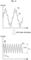
- FIG. 13 shows a state where the second angle detection signal S 2 c is generated based on S 2 b 1 and S 2 b 2 output from the pair of second angle detection sensors 12 A and 12 B.
- the second angle detection signal S 2 c corresponds to a signal obtained by doubling an amplitude of the signal obtained by removing the vibration noise RN 2 from the signal S 2 b 1 .
- the second angle detection signal S 2 c output from the second signal processing portion 61 B has a delay of 90° in phase with respect to the driving voltage waveform V 2A (t) included in the second driving signal as shown in FIG. 13 .
- the first phase shift portion 62 A shifts phases of the driving voltage waveforms output from the first driving signal generation portion 60 A. For example, the first phase shift portion 62 A shifts the phases by 90°.
- the second phase shift portion 62 B shifts phases of the driving voltage waveforms output from the second driving signal generation portion 60 B. For example, the second phase shift portion 62 B shifts the phases by 90°.
- the first angle derivation portion 63 A derives the angle (hereinafter, referred to as a “first angle”) of the mirror portion 20 around the first axis a 1 based on the first angle detection signal S 1 c . Specifically, the first angle derivation portion 63 A obtains a peak to peak (P-P) value V p-p1 corresponding to an amplitude of the first angle detection signal S 1 c (see FIG. 12 ). The first angle derivation portion 63 A holds data indicating a relationship between the first angle and the P-P value of the first angle detection signal S 1 c shown in FIG. 14 as an example.
- the first angle derivation portion 63 A derives a first angle ⁇ m1 corresponding to the P-P value V p-p1 obtained from the first angle detection signal S 1 c .
- the first angle derived by the first angle derivation portion 63 A according to the present embodiment corresponds to a double of a maximum value (that is, the first deflection angle) of the angle of the mirror portion 20 around the first axis a 1 in a cycle of the first angle.
- the second angle derivation portion 63 B derives the angle (hereinafter, referred to as a “second angle”) of the mirror portion 20 around the second axis a 2 based on the second angle detection signal S 2 c . Specifically, the second angle derivation portion 63 B obtains a P-P value V p-p2 corresponding to an amplitude of the second angle detection signal S 2 c (see FIG. 13 ). In the same manner as the first angle derivation portion 63 A, the second angle derivation portion 63 B also holds data indicating a relationship between the second angle and the P-P value of the second angle detection signal S 2 c .
- the second angle derivation portion 63 B derives the second angle corresponding to the P-P value V p-p2 obtained from the second angle detection signal S 2 c .
- the second angle derived by the second angle derivation portion 63 B according to the present embodiment corresponds to a double of a maximum value (that is, the second deflection angle) of the angle of the mirror portion 20 around the second axis a 2 in a cycle of the second angle.
- the first derivation portion 64 A acquires a phase difference between the first driving signal and the first angle detection signal S 1 c when the first angle in a case of providing the first driving signal to the first actuators 31 while changing only the first driving frequency out of the first driving frequency and the second driving frequency is the maximum, as a reference value (hereinafter referred to as a “first reference value”).
- first reference value a reference value
- the second driving signal is not provided to the second actuators 32 . That is, the first derivation portion 64 A acquires the first reference value by causing the mirror portion 20 to swing around only the first axis a 1 and not swing around the second axis a 2 .
- the first derivation portion 64 A acquires the first angle that is derived by the first angle derivation portion 63 A in a case of providing the first driving signal to the first actuators 31 while changing only the first driving frequency.
- the first angle is acquired for each of a plurality of first driving frequencies.
- a maximum first angle ⁇ 1max is obtained when the first driving frequency is f d1max .
- the first derivation portion 64 A derives a phase difference between the first driving signal having the first driving frequency when the first angle is the maximum among the acquired plurality of first driving frequencies and the first angles, and the first angle detection signal S 1 c detected when the first driving signal is provided to the first actuators 31 , as the first reference value.
- the first derivation portion 64 A derives the first reference value as a positive value based on the first driving signal. Specifically, as shown in FIG. 16 as an example, a time t 1 from a point in time when the first driving signal having the first driving frequency of f d1max is zero to a point in time when the first angle detection signal S 1 c is zero in a corresponding cycle is derived as the first reference value.
- the first driving signal is offset by an amount corresponding to the bias voltage V off1 .
- the point in time when the first driving signal is zero means a point in time when the first driving signal is V off1 .
- the first reference value may be a statistical value such as an average value, a mode, or a median of the time t 1 in a plurality of cycles.
- the first derivation portion 64 A derives the driving condition (hereinafter, referred to as a “first driving condition”) of the first actuators 31 under which the first driving frequency is less than the resonance frequency (hereinafter, referred to as a “first resonance frequency”) around the first axis a 1 .
- the first driving condition may be the driving voltage (hereinafter, referred to as a “first driving voltage”) of the first driving signal, the first driving frequency, or both of the first driving voltage and the first driving frequency.
- the driving voltage of the first driving signal corresponds to an amplitude of the first driving signal.
- the first derivation portion 64 A derives the first driving condition under which the phase difference (hereinafter, referred to as a “first phase difference”) between the first driving signal and the first angle detection signal S 1 c is less than the first reference value. This is because it is difficult to directly obtain the first resonance frequency, and the first driving frequency when the first phase difference is the first reference value is regarded as the first resonance frequency.
- the first derivation portion 64 A derives the first driving frequency with which the first phase difference is less than the first reference value at a preset driving voltage, as an initial setting value before the drawing of the image. For example, the first derivation portion 64 A sets the first driving voltage as a preset voltage value and finds the first driving frequency with which the first phase difference at a time of providing the first driving signal to the first actuators 31 while changing the first driving frequency is less than the first reference value.
- the first derivation portion 64 A derives the first driving condition under which after the first actuators are driven based on the derived initial setting value, the first angle is an angle within a preset range and the first phase difference is less than the first reference value.
- the first derivation portion 64 A derives a voltage value higher than the current voltage value as the first driving voltage. In a case where the first angle exceeds an upper limit value of the preset range, the first derivation portion 64 A derives a voltage value lower than the current voltage value as the first driving voltage. At this point, the first derivation portion 64 A derives the first driving condition under which the first phase difference is less than the first reference value, based on a value V 1 that represents a degree to which the immediately previous first phase difference is smaller than the first reference value.
- the first derivation portion 64 A in deriving the first driving condition, in a case where it is estimated that the first phase difference does not become less than the first reference value by changing only the voltage value of the first driving voltage based on the value V 1 , the first derivation portion 64 A derives a value obtained by also changing the first driving frequency.
- the first derivation portion 64 A repeats this processing of deriving the first driving condition a plurality of times. Accordingly, the first driving condition under which the first angle falls within the preset range and the first driving frequency is less than the first resonance frequency is derived before the drawing of the image.
- the first derivation portion 64 A may repeat the processing of deriving the first driving condition a plurality of times even during the drawing of the image.
- the second derivation portion 64 B acquires a phase difference between the second driving signal and the second angle detection signal S 2 c when the second angle in a case of providing the second driving signal to the second actuators 32 while changing only the second driving frequency out of the first driving frequency and the second driving frequency is the maximum, as the reference value (hereinafter referred to as a “second reference value”).
- the first driving signal is not provided to the first actuators 31 . That is, the second derivation portion 64 B acquires the second reference value by causing the mirror portion 20 to swing around only the second axis a 2 and not swing around the first axis a 1 .
- the second derivation portion 64 B acquires the second angle that is derived by the second angle derivation portion 63 B in a case of providing the second driving signal to the second actuators 32 while changing only the second driving frequency.
- the second angle is acquired for each of a plurality of second driving frequencies in the same manner as the processing performed by the first derivation portion 64 A.
- the second driving frequency when the second angle is the maximum among combinations of the plurality of second driving frequencies and the second angles will be denoted by f d2max .
- the second derivation portion 64 B derives a phase difference between the second driving signal having the second driving frequency when the second angle is the maximum among the acquired plurality of second driving frequencies and the second angles, and the second angle detection signal S 2 c detected when the second driving signal is provided to the second actuators 32 , as the second reference value.
- the second derivation portion 64 B derives the second reference value as a positive value based on the second driving signal Specifically, as shown in FIG. 17 as an example, a time t 2 from a point in time when the second driving signal having the second driving frequency of f d2max , is zero to a point in time when the second angle detection signal S 2 c is zero in a corresponding cycle is derived as the second reference value.
- the second driving signal is offset by an amount corresponding to the bias voltage V off2 .
- the point in time when the second driving signal is zero means a point in time when the second driving signal is V off2 .
- the second reference value may be a statistical value such as an average value, a mode, or a median of the time t 2 in a plurality of cycles.
- the second derivation portion 64 B derives the driving condition (hereinafter, referred to as a “second driving condition”) of the second actuators 32 under which the second driving frequency is greater than the resonance frequency (hereinafter, referred to as a “second resonance frequency”) around the second axis a 2 .
- the second driving condition may be the driving voltage (hereinafter, referred to as a “second driving voltage”) of the second driving signal, the second driving frequency, or both of the second driving voltage and the second driving frequency.
- the driving voltage of the second driving signal corresponds to an amplitude of the second driving signal.
- the second derivation portion 64 B derives the second driving condition under which the phase difference (hereinafter, referred to as a “second phase difference”) between the second driving signal and the second angle detection signal S 2 c is greater than the second reference value. This is because it is difficult to directly obtain the second resonance frequency, and the second driving frequency when the second phase difference is the second reference value is regarded as the second resonance frequency.
- the second derivation portion 64 B derives the second driving frequency with which the second phase difference is greater than the second reference value at a preset driving voltage, as an initial setting value before the drawing of the image. For example, the second derivation portion 64 B sets the second driving voltage as a preset voltage value and finds the second driving frequency with which the second phase difference is greater than the second reference value, by providing the second driving signal to the second actuators 32 while changing the second driving frequency.
- the second derivation portion 64 B derives the second driving condition under which after the second actuators 32 are driven based on the derived initial setting value, the second angle is an angle within a preset range and the second phase difference is greater than the second reference value.
- the second derivation portion 64 B derives a voltage value higher than the current voltage value as the second driving voltage. In a case where the second angle exceeds an upper limit value of the preset range, the second derivation portion 64 B derives a voltage value lower than the current voltage value as the second driving voltage. At this point, the second derivation portion 64 B derives the second driving condition under which the second phase difference is greater than the second reference value, based on a value V 2 that represents a degree to which the immediately previous second phase difference is greater than the second reference value.
- the second derivation portion 64 B in deriving the second driving condition, in a case where it is estimated that the second phase difference does not become greater than the second reference value by changing only the voltage value of the second driving voltage based on the value V 2 , the second derivation portion 64 B derives a value obtained by also changing the second driving frequency.
- the second derivation portion 64 B repeats this processing of deriving the second driving condition a plurality of times. Accordingly, the second driving condition under which the second angle falls within the preset range and the second driving frequency is greater than the second resonance frequency is derived before the drawing of the image.
- the second resonance frequency may change due to an influence of the ambient temperature or the like.
- the second derivation portion 64 B may repeat the processing of deriving the second driving condition a plurality of times even during the drawing of the image.
- the first zero cross pulse output portion 65 A generates a reference signal (hereinafter, referred to as a “first reference signal”) based on the first angle detection signal S 1 c .
- the first reference signal is a signal representing that the angle of the mirror portion 20 around the first axis a 1 is equal to a reference angle. In the present embodiment, an example of applying zero as this reference angle will be described. That is, the first zero cross pulse output portion 65 A generates a zero cross pulse (hereinafter, referred to as a “first zero cross pulse”) ZC 1 as an example of the first reference signal based on the first angle detection signal S 1 c .
- the first zero cross pulse output portion 65 A is configured with a zero cross detection circuit.
- the first zero cross pulse is a zero cross signal representing that the angle of the mirror portion 20 around the first axis a 1 is zero.
- the first zero cross pulse output portion 65 A generates the first zero cross pulse ZC 1 at a timing at which the first angle detection signal S 1 c crosses zero.
- the first zero cross pulse output portion 65 A outputs the generated first zero cross pulse ZC 1 to the light source driving portion 66 .
- the second zero cross pulse output portion 65 B generates a reference signal (hereinafter, referred to as a “second reference signal”) based on the second angle detection signal S 2 c .
- the second reference signal is a signal representing that the angle of the mirror portion 20 around the second axis as is equal to the reference angle.
- the second zero cross pulse output portion 65 B generates a zero cross pulse (hereinafter, referred to as a “second zero cross pulse”) ZC 2 as an example of the second reference signal based on the second angle detection signal S 2 c .
- the second zero cross pulse output portion 65 B is configured with a zero cross detection circuit.
- the second zero cross pulse is a zero cross signal representing that the angle of the mirror portion 20 around the second axis a 2 is zero.
- first zero cross pulse output portion 65 A and the second zero cross pulse output portion 65 B output the zero cross pulses at both of the timing when the sinusoidal wave becomes zero from a negative value toward a positive value and the timing when the sinusoidal wave becomes zero from a positive value toward a negative value
- the present disclosure is not limited thereto.
- the first zero cross pulse output portion 65 A and the second zero cross pulse output portion 65 B may output the zero cross pulses at any one of the timing when the sinusoidal wave becomes zero from a negative value toward a positive value and the timing when the sinusoidal wave becomes zero from a positive value toward a negative value.
- the light source driving portion 66 drives the light source 3 based on, for example, drawing data supplied from an outside of the image drawing system 10 .
- the light source driving portion 66 controls an irradiation timing of the laser light by the light source 3 so that the irradiation timing is synchronized with the first zero cross pulse ZC 1 and the second zero cross pulse ZC 2 . Accordingly, the image is drawn on the surface to be scanned 6 .
- the reference value derivation processing is executed when the optical scanning device 2 is started or at a timing at which an execution instruction is input by a user.
- step S 10 in FIG. 20 the first driving signal generation portion 60 A generates the first driving signal and provides the generated first driving signal to the pair of first actuators 31 through the first phase shift portion 62 A. Accordingly, the mirror portion 20 swings around only the first axis a 1 and does not swing around the second axis a 2 .
- step S 12 the first angle derivation portion 63 A derives the first angle based on the first angle detection signal S 1 c .
- the processing in steps S 10 and S 12 is repeatedly executed while the first driving frequency is changed. Accordingly, the first angle is acquired for each of the plurality of first driving frequencies. In a case the repetition of the processing in steps S 10 and S 12 is finished, the first driving signal generation portion 60 A stops generating the first driving signal.
- step S 14 the first derivation portion 64 A derives the phase difference between the first driving signal having the first driving frequency when the first angle is the maximum among the plurality of first driving frequencies and the first angles acquired by the repetition of the processing in steps S 10 and S 12 , and the first angle detection signal S 1 c detected when the first driving signal is provided to the first actuators 31 , as the first reference value.
- step S 16 the second driving signal generation portion 60 B generates the second driving signal and provides the generated second driving signal to the pair of second actuators 32 through the second phase shift portion 62 B. Accordingly, the mirror portion 20 swings around only the second axis a 2 and does not swing around the first axis a 1 .
- step S 18 the second angle derivation portion 63 B derives the second angle based on the second angle detection signal S 2 c .
- the processing in steps S 16 and S 18 is repeatedly executed while the second driving frequency is changed. Accordingly, the second angle is acquired for each of the plurality of second driving frequencies. In a case the repetition of the processing in steps S 16 and S 18 is finished, the second driving signal generation portion 60 B stops generating the second driving signal.
- step S 20 the second derivation portion 64 B derives the phase difference between the second driving signal having the second driving frequency when the second angle is the maximum among the plurality of second driving frequencies and the second angles acquired by the repetition of the processing in steps S 16 and S 18 , and the second angle detection signal S 2 c detected when the second driving signal is provided to the second actuators 32 , as the second reference value.
- the reference value derivation processing is finished.
- initial setting value derivation processing is executed before the drawing of the image after the execution of the reference value derivation processing is finished.
- step S 30 in FIG. 21 the first driving signal generation portion 60 A generates the first driving signal having the preset driving voltage and provides the generated first driving signal to the pair of first actuators 31 through the first phase shift portion 62 A.
- step S 32 the first derivation portion 64 A derives the first phase difference.
- the processing in steps S 30 and S 32 is repeatedly executed while the first driving frequency is changed. Accordingly, the first phase difference is acquired for each of the plurality of first driving frequencies. In a case the repetition of the processing in steps S 30 and S 32 is finished, the first driving signal generation portion 60 A stops generating the first driving signal.
- step S 34 the first derivation portion 64 A finds the first driving frequency with which the first phase difference is less than the first reference value derived in step S 14 , from a result of the repetition of the processing in steps S 30 and S 32 as the initial setting value of the first driving condition. Accordingly, the first derivation portion 64 A derives the first driving frequency as the initial setting value.
- the preset driving voltage and the first driving frequency derived in step S 34 are the initial setting value of the first driving condition.
- step S 36 the second driving signal generation portion 60 B generates the second driving signal having the preset driving voltage and provides the generated second driving signal to the pair of second actuators 32 through the second phase shift portion 62 B.
- step S 38 the second derivation portion 64 B derives the second phase difference.
- the processing in steps S 36 and S 38 is repeatedly executed while the second driving frequency is changed. Accordingly, the second phase difference is acquired for each of the plurality of second driving frequencies. In a case the repetition of the processing in steps S 36 and S 38 is finished, the second driving signal generation portion 60 B stops generating the second driving signal.
- step S 40 the second derivation portion 64 B finds the second driving frequency with which the second phase difference is greater than the second reference value derived in step S 20 , from a result of the repetition of the processing in steps S 36 and S 38 as the initial setting value of the second driving condition. Accordingly, the second derivation portion 64 B derives the second driving frequency as the initial setting value.
- the preset driving voltage and the second driving frequency derived in step S 40 are the initial setting value of the second driving condition. In a case where the processing in step S 40 is finished, the initial setting value derivation processing is finished.
- first driving condition derivation processing is executed before the drawing of the image after the execution of the initial setting value derivation processing is finished.
- step S 54 the first derivation portion 64 A determines whether or not the first angle derived in step S 52 is within the preset range.
- this range is set in advance in accordance with a length of the image drawn on the surface to be scanned 6 in the X direction. In a case where this determination results in a negative determination, the processing transitions to step S 56 .
- step S 56 the first derivation portion 64 A derives the first driving condition under which the first angle is an angle within the preset range and the first phase difference is less than the first reference value.
- the first driving frequency and the first driving voltage are changed in accordance with the first driving condition.
- the first driving condition derivation processing is finished.
- the determination in step S 54 results in a positive determination
- the first driving condition derivation processing is finished.
- the processing in steps S 52 to S 56 is repeatedly executed a plurality of times. Accordingly, the first driving condition under which the first angle falls within the preset range and the first phase difference is less than the first reference value is set.
- the processing in steps S 52 to S 56 of the first driving condition derivation processing may be repeatedly executed even during the drawing of the image.
- Examples of an execution interval in this case include a time interval corresponding to one cycle or a plurality of cycles of the first driving frequency.
- the second driving condition derivation processing is executed before the drawing of the image after the execution of the initial setting value derivation processing is finished.
- step S 60 in FIG. 23 the second driving signal generation portion 60 B generates the second driving signal in accordance with the initial setting value derived in step S 40 and provides the generated second driving signal to the pair of second actuators 32 through the second phase shift portion 62 B.
- step S 62 as described above, the second angle derivation portion 63 B derives the second angle based on the second angle detection signal S 2 c.
- step S 64 the second derivation portion 64 B determines whether or not the second angle derived in step S 62 is within the preset range.
- this range is set in advance in accordance with a length of the image drawn on the surface to be scanned 6 in the Y direction. In a case where this determination results in a negative determination, the processing transitions to step S 66 .
- step S 66 the second derivation portion 64 B derives the second driving condition under which the second angle is an angle within the preset range and the second phase difference is greater than the second reference value.
- the second driving frequency and the second driving voltage are changed in accordance with the second driving condition.
- the second driving condition derivation processing is finished.
- the determination in step S 64 results in a positive determination
- the second driving condition derivation processing is finished.
- the processing in steps S 62 to S 66 is repeatedly executed a plurality of times. Accordingly, the second driving condition under which the second angle falls within the preset range and the second phase difference is greater than the second reference value is set.
- the processing in steps S 62 to S 66 of the second driving condition derivation processing may be repeatedly executed even during the drawing of the image.
- Examples of an execution interval in this case include a time interval corresponding to one cycle or a plurality of cycles of the second driving frequency.
- the first actuators 31 are driven in accordance with the first driving condition under which the first driving frequency is less than the first resonance frequency. Accordingly, since the first driving frequency exceeding the first resonance frequency is suppressed, a rapid change in first deflection angle is suppressed. Accordingly, the image can be stably drawn.
- the configuration of the MMD 4 shown in the embodiment is an example.
- the configuration of the MMD 4 can be variously modified.
- the first actuators 31 that cause the mirror portion 20 to swing around the first axis a 1 may be arranged in the second movable frame 24
- the second actuators 32 that cause the mirror portion 20 to swing around the second axis a 2 may be arranged in the first movable frame 22 .
- the pair of first angle detection sensors 11 A and 11 B are arranged at positions that face each other with the first axis a 1 interposed therebetween is described, the present disclosure is not limited thereto.
- the pair of first angle detection sensors 11 A and 11 B may be arranged at positions that face each other with the second axis a 2 interposed therebetween.
- each of the pair of first angle detection sensors 11 A and 11 B is arranged near the first support portions 21 on the first movable frame 22 .
- the first angle detection sensor 11 A is arranged near the first support portion 21 connected to one side of the mirror portion 20 .
- the first angle detection sensor 11 B is arranged near the first support portion 21 connected to the other side of the mirror portion 20 . Accordingly, the pair of first angle detection sensors 11 A and 11 B are arranged at positions that face each other with the second axis a 2 interposed therebetween and face each other with the mirror portion 20 interposed therebetween. In addition, the pair of first angle detection sensors 11 A and 11 B are arranged at positions that are shifted in the same direction (in the example in FIG. 24 , the ⁇ X direction) from the first axis a 1 .
- the vibration noise can be removed by subtracting one of the output signals of both of the first angle detection sensors 11 A and 11 B from the other.
- the vibration noise can be removed by adding the output signals of both of the first angle detection sensors 11 A and 11 B.
- FIG. 25 An example of a configuration of the first signal processing portion 61 A in this form example is shown in FIG. 25 .
- the first signal processing portion 61 A includes an addition circuit 73 A instead of the subtraction circuit 73 .
- the addition circuit 73 A outputs a value obtained by adding the signal S 1 b 1 input from the first angle detection sensor 11 A through the buffer amplifier 71 to the signal S 1 b 2 input from the first angle detection sensor 11 B through the variable gain amplifier 72 .
- the pair of second angle detection sensors 12 A and 12 B may be arranged at positions that face each other with the second axis a 1 interposed therebetween.
- each of the pair of second angle detection sensors 12 A and 12 B is arranged near the second support portions 23 on the second movable frame 24 .
- the second angle detection sensor 12 A is arranged near the second support portion 23 connected to one side of the first movable frame 22 .
- the second angle detection sensor 12 B is arranged near the second support portion 23 connected to the other side of the first movable frame 22 . Accordingly, the pair of second angle detection sensors 12 A and 12 B are arranged at positions that face each other with the first axis a 1 interposed therebetween and face each other with the mirror portion 20 and the first movable frame 22 interposed therebetween. In addition, the pair of second angle detection sensors 12 A and 12 B are arranged at positions that are shifted in the same direction (in the example in FIG. 24 , the +Y direction) from the second axis a 2 .
- the vibration noise can be removed by subtracting one of the output signals of both of the second angle detection sensors 12 A and 12 B from the other.
- the vibration noise can be removed by adding the output signals of both of the second angle detection sensors 12 A and 12 B.
- a configuration of the second signal processing portion 61 B in this form example can be implemented by the same configuration as the first signal processing portion 61 A shown in FIG. 25 and thus, will not be described.
- a form of providing any one of the pair of first angle detection sensors 11 A and 11 B in the MMD 4 may be applied.
- a form of providing any one of the pair of second angle detection sensors 12 A and 12 B in the MMD 4 may be applied.
- the first driving condition and the second driving condition having the lowest power consumption are selected.
- the driving controller 5 can be configured using at least one of an analog operation circuit or a digital operation circuit.
- the driving controller 5 may be configured with one processor or may be configured with a combination of two or more processors of the same type or different types.
- Examples of the processor include a central processing unit (CPU), a programmable logic device (PLD), and a dedicated electric circuit.
- the CPU is a general-purpose processor that executes software (program) to function as various processing portions.
- the PLD is a processor such as a field programmable gate array (FPGA) that has a circuit configuration changeable after manufacturing.
- the dedicated electric circuit is a processor such as an application specific integrated circuit (ASIC) that has a circuit configuration dedicatedly designed to perform specific processing.
- ASIC application specific integrated circuit
Landscapes
- Physics & Mathematics (AREA)
- Optics & Photonics (AREA)
- General Physics & Mathematics (AREA)
- Engineering & Computer Science (AREA)
- Multimedia (AREA)
- Signal Processing (AREA)
- Power Engineering (AREA)
- Mechanical Optical Scanning Systems (AREA)
- Mechanical Light Control Or Optical Switches (AREA)
- Micromachines (AREA)
- Control Of Indicators Other Than Cathode Ray Tubes (AREA)
Abstract
Description
V 1A(t)=V off1 +V 1 sin(2πf d1 t)
V 1B(t)=V off1 +V 1 sin(2πf d1 t+α)
V 2A(t)=V off2 +V 2 sin(2πf d2 t+φ)
V 2B(t)=V off2 +V 2 sin(2πf d2 t+β+φ)
Claims (19)
Applications Claiming Priority (2)
| Application Number | Priority Date | Filing Date | Title |
|---|---|---|---|
| JP2021092418A JP7612521B2 (en) | 2021-06-01 | 2021-06-01 | Optical scanning device, driving method for optical scanning device, and image drawing system |
| JP2021-092418 | 2021-06-01 |
Publications (2)
| Publication Number | Publication Date |
|---|---|
| US20220382043A1 US20220382043A1 (en) | 2022-12-01 |
| US12320971B2 true US12320971B2 (en) | 2025-06-03 |
Family
ID=81598006
Family Applications (1)
| Application Number | Title | Priority Date | Filing Date |
|---|---|---|---|
| US17/738,515 Active 2043-11-02 US12320971B2 (en) | 2021-06-01 | 2022-05-06 | Optical scanning device, driving method of optical scanning device, and image drawing system |
Country Status (4)
| Country | Link |
|---|---|
| US (1) | US12320971B2 (en) |
| EP (1) | EP4099082A1 (en) |
| JP (1) | JP7612521B2 (en) |
| CN (1) | CN115437141A (en) |
Families Citing this family (5)
| Publication number | Priority date | Publication date | Assignee | Title |
|---|---|---|---|---|
| JP7436686B2 (en) * | 2020-09-04 | 2024-02-22 | 富士フイルム株式会社 | Micromirror device and optical scanning device |
| JP7612521B2 (en) * | 2021-06-01 | 2025-01-14 | 富士フイルム株式会社 | Optical scanning device, driving method for optical scanning device, and image drawing system |
| JPWO2024202829A1 (en) * | 2023-03-27 | 2024-10-03 | ||
| JPWO2024247568A1 (en) * | 2023-05-29 | 2024-12-05 | ||
| IT202300017949A1 (en) * | 2023-08-31 | 2025-03-03 | St Microelectronics Int Nv | HIGH FREQUENCY BI-AXIAL BI-RESONANT MIRROR MICROELECTROMECHANICAL STRUCTURE |
Citations (34)
| Publication number | Priority date | Publication date | Assignee | Title |
|---|---|---|---|---|
| JP2003004851A (en) | 2001-04-16 | 2003-01-08 | Nissan Motor Co Ltd | Radar equipment |
| JP2007226108A (en) | 2006-02-27 | 2007-09-06 | Ricoh Co Ltd | Optical scanning apparatus and image forming apparatus |
| US20080297868A1 (en) | 2007-05-28 | 2008-12-04 | Konica Minolta Opto, Inc. | Image display apparatus |
| JP2011118250A (en) | 2009-12-04 | 2011-06-16 | Seiko Epson Corp | Optical scanner |
| JP2012237788A (en) | 2011-05-10 | 2012-12-06 | Konica Minolta Advanced Layers Inc | Optical scanner and image projection device equipped with the same |
| JP2013235161A (en) | 2012-05-09 | 2013-11-21 | Jvc Kenwood Corp | Manufacturing method of mems optical scanner |
| US20160011290A1 (en) * | 2013-05-21 | 2016-01-14 | Victor Iannello | Non-Invasive, In-Vivo Measurement of Blood Constituents Using a Portable Nuclear Magnetic Resonance Device |
| JP2016156913A (en) | 2015-02-24 | 2016-09-01 | 日本信号株式会社 | Optical scanning device |
| JP2016184018A (en) | 2015-03-25 | 2016-10-20 | 株式会社豊田中央研究所 | Optical deflection device, light irradiation device, and distance measurement device |
| US20180176524A1 (en) | 2016-12-20 | 2018-06-21 | Hitachi-Lg Data Storage, Inc. | Laser projection display device |
| WO2019163754A1 (en) | 2018-02-20 | 2019-08-29 | パイオニア株式会社 | Mirror device, optical scanning device, distance-measuring device, control method for mirror device, and program |
| JP6833127B1 (en) | 2020-03-26 | 2021-02-24 | 三菱電機株式会社 | Optical scanning device, control method of optical scanning device, and distance measuring device |
| US20210058592A1 (en) * | 2019-08-20 | 2021-02-25 | Goichi Akanuma | Light deflector, optical scanning system, image projection device, image forming apparatus, and lidar device |
| US20210333542A1 (en) * | 2020-04-22 | 2021-10-28 | Stanley Electric Co., Ltd. | Light deflection device |
| US20210349284A1 (en) * | 2020-05-08 | 2021-11-11 | Mitsubishi Electric Corporation | Optical scanning device and adjustment method for optical scanning device |
| US20210405350A1 (en) * | 2019-03-28 | 2021-12-30 | Fujifilm Corporation | Micromirror device and method of driving micromirror device |
| US20220043257A1 (en) * | 2019-04-26 | 2022-02-10 | Fujifilm Corporation | Micromirror device |
| US20220326509A1 (en) * | 2021-04-13 | 2022-10-13 | Fujifilm Corporation | Micromirror device and optical scanning device |
| US20220382043A1 (en) * | 2021-06-01 | 2022-12-01 | Fujifilm Corporation | Optical scanning device, driving method of optical scanning device, and image drawing system |
| US20220404613A1 (en) * | 2021-06-18 | 2022-12-22 | Fujifilm Corporation | Optical scanning device, driving method of optical scanning device, and image drawing system |
| US20230074021A1 (en) * | 2021-09-08 | 2023-03-09 | Fujifilm Corporation | Micromirror device and optical scanning device |
| US20230139572A1 (en) * | 2020-07-16 | 2023-05-04 | Fujifilm Corporation | Optical scanning device and method of driving micromirror device |
| US20230152573A1 (en) * | 2020-04-06 | 2023-05-18 | Hamamatsu Photonics K.K. | Mems actuator, mems actuator drive method, and mems actuator control program |
| US20230221547A1 (en) * | 2022-01-11 | 2023-07-13 | Fujifilm Corporation | Optical scanning device and control method thereof |
| US20230221546A1 (en) * | 2022-01-11 | 2023-07-13 | Fujifilm Corporation | Optical scanning device and control method thereof |
| US20230305116A1 (en) * | 2022-03-28 | 2023-09-28 | Fujifilm Corporation | Optical scanning device, driving method of optical scanning device, and distance measurement device |
| US20230305293A1 (en) * | 2022-03-25 | 2023-09-28 | Fujifilm Corporation | Optical scanning device, driving method of optical scanning device, and image drawing system |
| US20230314793A1 (en) * | 2022-03-31 | 2023-10-05 | Fujifilm Corporation | Optical scanning device, driving method of optical scanning device, and image drawing system |
| US20230350193A1 (en) * | 2021-01-27 | 2023-11-02 | Fujifilm Corporation | Optical scanning device and method of driving micromirror device |
| US20240036305A1 (en) * | 2022-07-28 | 2024-02-01 | Fujifilm Corporation | Image projection device and control method for image projection device |
| US20240146317A1 (en) * | 2022-11-02 | 2024-05-02 | Infineon Technologies Ag | Method of synchronizing a fixed frequency ratio for a multi-axis scanner |
| US20240159877A1 (en) * | 2022-11-10 | 2024-05-16 | Infineon Technologies Ag | Admixture sensing method for gimbaled scanners |
| US20240241368A1 (en) * | 2021-05-18 | 2024-07-18 | Stanley Electric Co., Ltd. | Optical deflector driving system and optical deflector driving method |
| US20240288681A1 (en) * | 2021-07-13 | 2024-08-29 | Stanley Electric Co., Ltd. | Mems optical deflector and optical scanning device |
Family Cites Families (1)
| Publication number | Priority date | Publication date | Assignee | Title |
|---|---|---|---|---|
| TWI352823B (en) | 2007-05-09 | 2011-11-21 | Opus Microsystems Corp | Stabilizing oscillation amplitude of torsion oscil |
-
2021
- 2021-06-01 JP JP2021092418A patent/JP7612521B2/en active Active
-
2022
- 2022-05-06 US US17/738,515 patent/US12320971B2/en active Active
- 2022-05-09 EP EP22172413.1A patent/EP4099082A1/en active Pending
- 2022-05-24 CN CN202210568042.XA patent/CN115437141A/en active Pending
Patent Citations (35)
| Publication number | Priority date | Publication date | Assignee | Title |
|---|---|---|---|---|
| JP2003004851A (en) | 2001-04-16 | 2003-01-08 | Nissan Motor Co Ltd | Radar equipment |
| JP2007226108A (en) | 2006-02-27 | 2007-09-06 | Ricoh Co Ltd | Optical scanning apparatus and image forming apparatus |
| US20080297868A1 (en) | 2007-05-28 | 2008-12-04 | Konica Minolta Opto, Inc. | Image display apparatus |
| JP2011118250A (en) | 2009-12-04 | 2011-06-16 | Seiko Epson Corp | Optical scanner |
| JP2012237788A (en) | 2011-05-10 | 2012-12-06 | Konica Minolta Advanced Layers Inc | Optical scanner and image projection device equipped with the same |
| JP2013235161A (en) | 2012-05-09 | 2013-11-21 | Jvc Kenwood Corp | Manufacturing method of mems optical scanner |
| US20160011290A1 (en) * | 2013-05-21 | 2016-01-14 | Victor Iannello | Non-Invasive, In-Vivo Measurement of Blood Constituents Using a Portable Nuclear Magnetic Resonance Device |
| JP2016156913A (en) | 2015-02-24 | 2016-09-01 | 日本信号株式会社 | Optical scanning device |
| JP2016184018A (en) | 2015-03-25 | 2016-10-20 | 株式会社豊田中央研究所 | Optical deflection device, light irradiation device, and distance measurement device |
| US20180176524A1 (en) | 2016-12-20 | 2018-06-21 | Hitachi-Lg Data Storage, Inc. | Laser projection display device |
| JP2018101040A (en) | 2016-12-20 | 2018-06-28 | 株式会社日立エルジーデータストレージ | Laser projection display device |
| WO2019163754A1 (en) | 2018-02-20 | 2019-08-29 | パイオニア株式会社 | Mirror device, optical scanning device, distance-measuring device, control method for mirror device, and program |
| US20210405350A1 (en) * | 2019-03-28 | 2021-12-30 | Fujifilm Corporation | Micromirror device and method of driving micromirror device |
| US20220043257A1 (en) * | 2019-04-26 | 2022-02-10 | Fujifilm Corporation | Micromirror device |
| US20210058592A1 (en) * | 2019-08-20 | 2021-02-25 | Goichi Akanuma | Light deflector, optical scanning system, image projection device, image forming apparatus, and lidar device |
| JP6833127B1 (en) | 2020-03-26 | 2021-02-24 | 三菱電機株式会社 | Optical scanning device, control method of optical scanning device, and distance measuring device |
| US20230152573A1 (en) * | 2020-04-06 | 2023-05-18 | Hamamatsu Photonics K.K. | Mems actuator, mems actuator drive method, and mems actuator control program |
| US20210333542A1 (en) * | 2020-04-22 | 2021-10-28 | Stanley Electric Co., Ltd. | Light deflection device |
| US20210349284A1 (en) * | 2020-05-08 | 2021-11-11 | Mitsubishi Electric Corporation | Optical scanning device and adjustment method for optical scanning device |
| US20230139572A1 (en) * | 2020-07-16 | 2023-05-04 | Fujifilm Corporation | Optical scanning device and method of driving micromirror device |
| US20230350193A1 (en) * | 2021-01-27 | 2023-11-02 | Fujifilm Corporation | Optical scanning device and method of driving micromirror device |
| US20220326509A1 (en) * | 2021-04-13 | 2022-10-13 | Fujifilm Corporation | Micromirror device and optical scanning device |
| US20240241368A1 (en) * | 2021-05-18 | 2024-07-18 | Stanley Electric Co., Ltd. | Optical deflector driving system and optical deflector driving method |
| US20220382043A1 (en) * | 2021-06-01 | 2022-12-01 | Fujifilm Corporation | Optical scanning device, driving method of optical scanning device, and image drawing system |
| US20220404613A1 (en) * | 2021-06-18 | 2022-12-22 | Fujifilm Corporation | Optical scanning device, driving method of optical scanning device, and image drawing system |
| US20240288681A1 (en) * | 2021-07-13 | 2024-08-29 | Stanley Electric Co., Ltd. | Mems optical deflector and optical scanning device |
| US20230074021A1 (en) * | 2021-09-08 | 2023-03-09 | Fujifilm Corporation | Micromirror device and optical scanning device |
| US20230221547A1 (en) * | 2022-01-11 | 2023-07-13 | Fujifilm Corporation | Optical scanning device and control method thereof |
| US20230221546A1 (en) * | 2022-01-11 | 2023-07-13 | Fujifilm Corporation | Optical scanning device and control method thereof |
| US20230305293A1 (en) * | 2022-03-25 | 2023-09-28 | Fujifilm Corporation | Optical scanning device, driving method of optical scanning device, and image drawing system |
| US20230305116A1 (en) * | 2022-03-28 | 2023-09-28 | Fujifilm Corporation | Optical scanning device, driving method of optical scanning device, and distance measurement device |
| US20230314793A1 (en) * | 2022-03-31 | 2023-10-05 | Fujifilm Corporation | Optical scanning device, driving method of optical scanning device, and image drawing system |
| US20240036305A1 (en) * | 2022-07-28 | 2024-02-01 | Fujifilm Corporation | Image projection device and control method for image projection device |
| US20240146317A1 (en) * | 2022-11-02 | 2024-05-02 | Infineon Technologies Ag | Method of synchronizing a fixed frequency ratio for a multi-axis scanner |
| US20240159877A1 (en) * | 2022-11-10 | 2024-05-16 | Infineon Technologies Ag | Admixture sensing method for gimbaled scanners |
Non-Patent Citations (6)
| Title |
|---|
| European Communication pursuant to Article 94(3) EPC for European Application No. 22172413.1, dated Mar. 4, 2025. |
| Extended European Search Report for European Application No. 22172413.1, dated Nov. 2, 2022. |
| Japanese Office Action for Japanese Application No. 2021-092418, dated Oct. 1, 2024, with an English translation. |
| Mendicino et al., "Electro-mechanical validation of a resonant MEMS mirror with PZT actuation and PZR sensing," Proc. SPIE, MOEMS and Miniaturized Systems XX, vol. 11697, Mar. 5, 2021, total 17 pages. |
| Okuda et al., WO 2019/163754 English Machine Translation (Year: 2019). * |
| Seo et al., "Scanning MEMS Mirror for High Definition and High Frame Rate Lissajous Patterns," Micromachines, vol. 10, No. 67, 2019, pp. 1-8. |
Also Published As
| Publication number | Publication date |
|---|---|
| US20220382043A1 (en) | 2022-12-01 |
| CN115437141A (en) | 2022-12-06 |
| JP7612521B2 (en) | 2025-01-14 |
| JP2022184515A (en) | 2022-12-13 |
| EP4099082A1 (en) | 2022-12-07 |
Similar Documents
| Publication | Publication Date | Title |
|---|---|---|
| US12320971B2 (en) | Optical scanning device, driving method of optical scanning device, and image drawing system | |
| US12282155B2 (en) | Optical scanning device, driving method of optical scanning device, and image drawing system | |
| CN116209636B (en) | Optical scanning device, driving method thereof, and image drawing system | |
| US12159562B2 (en) | Optical scanning device, method of driving optical scanning device, and image drawing system | |
| US12401771B2 (en) | Optical scanning device, driving method of optical scanning device, and image drawing system | |
| US12302041B2 (en) | Optical scanning device, driving method of optical scanning device, and image drawing system | |
| US12422666B2 (en) | Optical scanning device, driving method of optical scanning device, and image drawing system | |
| CN112399159A (en) | Driving multi-resonant MEMS mirrors with a single frequency | |
| US20260009999A1 (en) | Optical scanning device, image drawing system, and driving method of mirror device | |
| US20250350699A1 (en) | Image drawing apparatus and driving method for image drawing apparatus | |
| WO2025074825A1 (en) | Optical scanning device and method for driving optical scanning device | |
| WO2025057631A1 (en) | Optical scanning apparatus, image drawing system, and method for driving optical scanning apparatus | |
| WO2025013508A1 (en) | Optical scanning device and method for driving optical scanning device |
Legal Events
| Date | Code | Title | Description |
|---|---|---|---|
| FEPP | Fee payment procedure |
Free format text: ENTITY STATUS SET TO UNDISCOUNTED (ORIGINAL EVENT CODE: BIG.); ENTITY STATUS OF PATENT OWNER: LARGE ENTITY |
|
| AS | Assignment |
Owner name: FUJIFILM CORPORATION, JAPAN Free format text: ASSIGNMENT OF ASSIGNORS INTEREST;ASSIGNORS:YOSHIZAWA, HIROTOSHI;SONODA, SHINICHIRO;HISHINUMA, YOSHIKAZU;AND OTHERS;REEL/FRAME:059868/0994 Effective date: 20220324 |
|
| STPP | Information on status: patent application and granting procedure in general |
Free format text: DOCKETED NEW CASE - READY FOR EXAMINATION |
|
| STPP | Information on status: patent application and granting procedure in general |
Free format text: NON FINAL ACTION MAILED |
|
| STPP | Information on status: patent application and granting procedure in general |
Free format text: RESPONSE TO NON-FINAL OFFICE ACTION ENTERED AND FORWARDED TO EXAMINER |
|
| STPP | Information on status: patent application and granting procedure in general |
Free format text: NOTICE OF ALLOWANCE MAILED -- APPLICATION RECEIVED IN OFFICE OF PUBLICATIONS |
|
| STCF | Information on status: patent grant |
Free format text: PATENTED CASE |