US12317666B2 - Organic thin film transistor and method of manufacturing the same and thin film transistor array panel and electronic device - Google Patents
Organic thin film transistor and method of manufacturing the same and thin film transistor array panel and electronic device Download PDFInfo
- Publication number
- US12317666B2 US12317666B2 US17/678,453 US202217678453A US12317666B2 US 12317666 B2 US12317666 B2 US 12317666B2 US 202217678453 A US202217678453 A US 202217678453A US 12317666 B2 US12317666 B2 US 12317666B2
- Authority
- US
- United States
- Prior art keywords
- thin film
- hydrophilic
- organic semiconductor
- nanolayer
- organic
- Prior art date
- Legal status (The legal status is an assumption and is not a legal conclusion. Google has not performed a legal analysis and makes no representation as to the accuracy of the status listed.)
- Active, expires
Links
Images


Classifications
-
- H—ELECTRICITY
- H10—SEMICONDUCTOR DEVICES; ELECTRIC SOLID-STATE DEVICES NOT OTHERWISE PROVIDED FOR
- H10K—ORGANIC ELECTRIC SOLID-STATE DEVICES
- H10K10/00—Organic devices specially adapted for rectifying, amplifying, oscillating or switching; Organic capacitors or resistors having potential barriers
- H10K10/80—Constructional details
- H10K10/88—Passivation; Containers; Encapsulations
-
- H—ELECTRICITY
- H10—SEMICONDUCTOR DEVICES; ELECTRIC SOLID-STATE DEVICES NOT OTHERWISE PROVIDED FOR
- H10K—ORGANIC ELECTRIC SOLID-STATE DEVICES
- H10K10/00—Organic devices specially adapted for rectifying, amplifying, oscillating or switching; Organic capacitors or resistors having potential barriers
- H10K10/40—Organic transistors
- H10K10/46—Field-effect transistors, e.g. organic thin-film transistors [OTFT]
- H10K10/462—Insulated gate field-effect transistors [IGFETs]
- H10K10/484—Insulated gate field-effect transistors [IGFETs] characterised by the channel regions
-
- H—ELECTRICITY
- H10—SEMICONDUCTOR DEVICES; ELECTRIC SOLID-STATE DEVICES NOT OTHERWISE PROVIDED FOR
- H10K—ORGANIC ELECTRIC SOLID-STATE DEVICES
- H10K10/00—Organic devices specially adapted for rectifying, amplifying, oscillating or switching; Organic capacitors or resistors having potential barriers
- H10K10/40—Organic transistors
- H10K10/46—Field-effect transistors, e.g. organic thin-film transistors [OTFT]
- H10K10/462—Insulated gate field-effect transistors [IGFETs]
- H10K10/481—Insulated gate field-effect transistors [IGFETs] characterised by the gate conductors
-
- H—ELECTRICITY
- H10—SEMICONDUCTOR DEVICES; ELECTRIC SOLID-STATE DEVICES NOT OTHERWISE PROVIDED FOR
- H10K—ORGANIC ELECTRIC SOLID-STATE DEVICES
- H10K10/00—Organic devices specially adapted for rectifying, amplifying, oscillating or switching; Organic capacitors or resistors having potential barriers
- H10K10/40—Organic transistors
- H10K10/46—Field-effect transistors, e.g. organic thin-film transistors [OTFT]
- H10K10/462—Insulated gate field-effect transistors [IGFETs]
- H10K10/466—Lateral bottom-gate IGFETs comprising only a single gate
-
- H—ELECTRICITY
- H10—SEMICONDUCTOR DEVICES; ELECTRIC SOLID-STATE DEVICES NOT OTHERWISE PROVIDED FOR
- H10K—ORGANIC ELECTRIC SOLID-STATE DEVICES
- H10K71/00—Manufacture or treatment specially adapted for the organic devices covered by this subclass
- H10K71/10—Deposition of organic active material
- H10K71/16—Deposition of organic active material using physical vapour deposition [PVD], e.g. vacuum deposition or sputtering
- H10K71/166—Deposition of organic active material using physical vapour deposition [PVD], e.g. vacuum deposition or sputtering using selective deposition, e.g. using a mask
-
- H—ELECTRICITY
- H10—SEMICONDUCTOR DEVICES; ELECTRIC SOLID-STATE DEVICES NOT OTHERWISE PROVIDED FOR
- H10K—ORGANIC ELECTRIC SOLID-STATE DEVICES
- H10K71/00—Manufacture or treatment specially adapted for the organic devices covered by this subclass
- H10K71/20—Changing the shape of the active layer in the devices, e.g. patterning
- H10K71/231—Changing the shape of the active layer in the devices, e.g. patterning by etching of existing layers
- H10K71/233—Changing the shape of the active layer in the devices, e.g. patterning by etching of existing layers by photolithographic etching
-
- H—ELECTRICITY
- H10—SEMICONDUCTOR DEVICES; ELECTRIC SOLID-STATE DEVICES NOT OTHERWISE PROVIDED FOR
- H10K—ORGANIC ELECTRIC SOLID-STATE DEVICES
- H10K77/00—Constructional details of devices covered by this subclass and not covered by groups H10K10/80, H10K30/80, H10K50/80 or H10K59/80
- H10K77/10—Substrates, e.g. flexible substrates
- H10K77/111—Flexible substrates
-
- H—ELECTRICITY
- H10—SEMICONDUCTOR DEVICES; ELECTRIC SOLID-STATE DEVICES NOT OTHERWISE PROVIDED FOR
- H10D—INORGANIC ELECTRIC SEMICONDUCTOR DEVICES
- H10D86/00—Integrated devices formed in or on insulating or conducting substrates, e.g. formed in silicon-on-insulator [SOI] substrates or on stainless steel or glass substrates
- H10D86/40—Integrated devices formed in or on insulating or conducting substrates, e.g. formed in silicon-on-insulator [SOI] substrates or on stainless steel or glass substrates characterised by multiple TFTs
- H10D86/471—Integrated devices formed in or on insulating or conducting substrates, e.g. formed in silicon-on-insulator [SOI] substrates or on stainless steel or glass substrates characterised by multiple TFTs having different architectures, e.g. having both top-gate and bottom-gate TFTs
-
- H—ELECTRICITY
- H10—SEMICONDUCTOR DEVICES; ELECTRIC SOLID-STATE DEVICES NOT OTHERWISE PROVIDED FOR
- H10D—INORGANIC ELECTRIC SEMICONDUCTOR DEVICES
- H10D86/00—Integrated devices formed in or on insulating or conducting substrates, e.g. formed in silicon-on-insulator [SOI] substrates or on stainless steel or glass substrates
- H10D86/40—Integrated devices formed in or on insulating or conducting substrates, e.g. formed in silicon-on-insulator [SOI] substrates or on stainless steel or glass substrates characterised by multiple TFTs
- H10D86/60—Integrated devices formed in or on insulating or conducting substrates, e.g. formed in silicon-on-insulator [SOI] substrates or on stainless steel or glass substrates characterised by multiple TFTs wherein the TFTs are in active matrices
-
- H—ELECTRICITY
- H10—SEMICONDUCTOR DEVICES; ELECTRIC SOLID-STATE DEVICES NOT OTHERWISE PROVIDED FOR
- H10K—ORGANIC ELECTRIC SOLID-STATE DEVICES
- H10K10/00—Organic devices specially adapted for rectifying, amplifying, oscillating or switching; Organic capacitors or resistors having potential barriers
- H10K10/40—Organic transistors
- H10K10/46—Field-effect transistors, e.g. organic thin-film transistors [OTFT]
- H10K10/462—Insulated gate field-effect transistors [IGFETs]
- H10K10/464—Lateral top-gate IGFETs comprising only a single gate
-
- H—ELECTRICITY
- H10—SEMICONDUCTOR DEVICES; ELECTRIC SOLID-STATE DEVICES NOT OTHERWISE PROVIDED FOR
- H10K—ORGANIC ELECTRIC SOLID-STATE DEVICES
- H10K2102/00—Constructional details relating to the organic devices covered by this subclass
Definitions
- a display device such as a liquid crystal display (LCD), an organic light emitting diode display (OLED display), or a quantum dot light emitting diode display includes a plurality of thin film transistors for independently switching and/or driving an element in each subpixel.
- OTFT organic thin film transistor
- the organic thin film transistor may be made into a fiber or a film due to characteristics of an organic material, and thus is drawing attention as a core element for a flexible display device.
- an organic thin film transistor In order to form an organic thin film transistor, a process of patterning an organic semiconductor may be performed.
- the organic semiconductor may be easily damaged by a chemical liquid used in the process, and the damaged organic semiconductor may deteriorate electrical characteristics of the organic thin film transistor.
- Some example embodiments provide an organic thin film transistor capable of reducing or preventing deterioration of electrical characteristics of the organic thin film transistor by reducing or preventing damage to the organic semiconductor during a process.
- Some example embodiments provide a method of manufacturing the organic thin film transistor capable of reducing or preventing damage to the organic semiconductor.
- Some example embodiments provide a thin film transistor array panel including the organic thin film transistor.
- Some example embodiments provide an electronic device including the organic thin film transistor or the thin film transistor array panel.
- an organic thin film transistor may include a gate electrode, an organic semiconductor layer overlapped with the gate electrode, a hydrophilic nanolayer on the organic semiconductor layer, and a source electrode and a drain electrode electrically connected to the organic semiconductor layer.
- the hydrophilic nanolayer may be in direct contact with an upper surface of the organic semiconductor layer and may cover all or a portion of the upper surface of the organic semiconductor layer.
- the hydrophilic nanolayer may include a hydrophilic inorganic material, a hydrophilic organic material, a hydrophilic organic-inorganic material, or any combination thereof.
- the hydrophilic inorganic material, the hydrophilic organic material, and the hydrophilic organic-inorganic material may be insoluble in water.
- the hydrophilic inorganic material, the hydrophilic organic material, and the hydrophilic organic-inorganic material may each be an electrical insulator.
- the hydrophilic nanolayer may include a metal oxide, a semi-metal oxide, or any combination thereof.
- a thickness of the hydrophilic nanolayer may be greater than or equal to about 1 nm and less than about 10 nm.
- the organic semiconductor layer may be hydrophobic.
- a method of manufacturing an organic thin film transistor may include forming a gate electrode, forming an organic semiconductor layer overlapped with the gate electrode, and forming a source electrode and a drain electrode electrically connected to the organic semiconductor layer, wherein the forming of the organic semiconductor layer includes forming an organic semiconductor thin film, forming a hydrophilic nanolayer on the organic semiconductor thin film, forming a protective interlayer on the hydrophilic nanolayer, performing a photolithography of the protective interlayer, the hydrophilic nanolayer, and the organic semiconductor thin film, and removing the protective interlayer.
- the performing the photolithography of the protective interlayer, the hydrophilic nanolayer, and the organic semiconductor thin film may include applying a photoresist film on the protective interlayer, disposing a mask on the photoresist film and exposing a portion of the photoresist film, developing the exposed portion of the photoresist film to form a photoresist pattern, patterning the protective interlayer, the hydrophilic nanolayer and the organic semiconductor thin film using the photoresist pattern, and removing the photoresist pattern.
- the photoresist film may include a fluorine-containing photoresist.
- the protective interlayer may include a material different from that in the hydrophilic nanolayer.
- the protective interlayer may include a water-soluble organic compound.
- the hydrophilic nanolayer may include a hydrophilic metal oxide, a hydrophilic low molecular weight compound, or any combination thereof, and the hydrophilic metal oxide and the hydrophilic low molecular weight compound may be insoluble in water.
- the hydrophilic nanolayer may be formed by vapor deposition, and the protective interlayer may be formed by a solution process.
- the removing of the protective interlayer may include supplying water to the protective interlayer.
- a thin film transistor array panel including the organic thin film transistor is provided.
- the thin film transistor array panel may further include a substrate supporting the organic thin film transistor, and the substrate may be a stretchable substrate.
- an electronic device including the organic thin film transistor or the thin film transistor array panel is provided.
- FIGS. 1 , 2 , 3 , 4 , 5 , 6 , 7 , and 8 are cross-sectional views showing examples of an organic thin film transistor according to some example embodiments.
- FIGS. 9 , 10 , 11 , 12 , 13 , 14 , 15 , 16 , 17 , and 18 are cross-sectional views sequentially showing an example of a method of manufacturing an organic thin film transistor according to some example embodiments.
- FIG. 19 is a schematic plan view of a thin film transistor array panel according to some example embodiments.
- Example embodiments will hereinafter be described in detail, and may be easily performed by a person having an ordinary skill in the related art. However, the inventive concepts may be embodied in many different forms and are not to be construed as limited to the example embodiments set forth herein.
- substituted refers to replacement of hydrogen of a compound by a substituent selected from a halogen, a hydroxy group, a nitro group, a cyano group, an amino group, an azido group, an amidino group, a hydrazino group, a hydrazono group, a carbonyl group, a carbamyl group, a thiol group, an ester group, a carboxyl group or a salt thereof, a sulfonic acid group or a salt thereof, a phosphoric acid or a salt thereof, a silyl group, a C1 to C30 alkyl group, a C2 to C30 alkenyl group, a C2 to C30 alkynyl group, a C6 to C30 aryl group, a C7 to C30 arylalkyl group, a C1 to C30 alkoxy group, a C1 to C1 to C
- hetero refers to inclusion of one to four heteroatoms selected from N, O, S, Se, Te, Si, and P.
- polymer includes a homopolymer, a copolymer, or any combination thereof.
- “combination” includes a mixture, a composite, or a stacked structure of two or more.
- elements and/or properties thereof e.g., structures, surfaces, directions, or the like
- elements and/or properties thereof which may be referred to as being “perpendicular,” “parallel,” “coplanar,” or the like with regard to other elements and/or properties thereof (e.g., structures, surfaces, directions, or the like) may be “perpendicular,” “parallel,” “coplanar,” or the like or may be “substantially perpendicular,” “substantially parallel,” “substantially coplanar,” respectively, with regard to the other elements and/or properties thereof.
- Elements and/or properties thereof e.g., structures, surfaces, directions, or the like
- are “substantially perpendicular” with regard to other elements and/or properties thereof will be understood to be “perpendicular” with regard to the other elements and/or properties thereof within manufacturing tolerances and/or material tolerances and/or have a deviation in magnitude and/or angle from “perpendicular,” or the like with regard to the other elements and/or properties thereof that is equal to or less than 10% (e.g., a. tolerance of ⁇ 10%).
- Elements and/or properties thereof e.g., structures, surfaces, directions, or the like
- are “substantially parallel” with regard to other elements and/or properties thereof will be understood to be “parallel” with regard to the other elements and/or properties thereof within manufacturing tolerances and/or material tolerances and/or have a deviation in magnitude and/or angle from “parallel,” or the like with regard to the other elements and/or properties thereof that is equal to or less than 10% (e.g., a. tolerance of ⁇ 10%).
- Elements and/or properties thereof that are “substantially identical” to, “substantially the same” as or “substantially equal” to other elements and/or properties thereof will be understood to include elements and/or properties thereof that are identical to, the same as, or equal to the other elements and/or properties thereof within manufacturing tolerances and/or material tolerances.
- Elements and/or properties thereof that are identical or substantially identical to and/or the same or substantially the same as other elements and/or properties thereof may be structurally the same or substantially the same, functionally the same or substantially the same, and/or compositionally the same or substantially the same.
- FIGS. 1 , 2 , 3 , 4 , 5 , 6 , 7 , and 8 are cross-sectional views showing examples of an organic thin film transistor according to some example embodiments.
- an organic thin film transistor 100 includes a gate electrode 124 on a substrate 110 ; an organic semiconductor layer 154 overlapped with the gate electrode 124 along the thickness direction of the substrate 110 (e.g., overlapped in the direction extending perpendicular to the upper surface of the substrate 110 that is proximate to the gate electrode 124 ); a hydrophilic nanolayer 155 on the organic semiconductor layer 154 ; a gate insulating film 140 between the gate electrode 124 and the organic semiconductor layer 154 ; and a source electrode 173 and a drain electrode 175 electrically connected to the organic semiconductor layer 154 .
- the organic thin film transistor 100 may be an organic thin film transistor having a bottom gate structure and a bottom contact structure, and specifically, includes a gate electrode 124 on a substrate 110 ; a gate insulating film 140 on the gate electrode 124 ; a source electrode 173 and a drain electrode 175 on the gate insulating film 140 ; an organic semiconductor layer 154 on the source electrode 173 and the drain electrode 175 ; and a hydrophilic nanolayer 155 on the organic semiconductor layer 154 .
- the substrate 110 may be a stretchable substrate that can be stretched in a predetermined direction and can be restored again.
- the stretchable substrate may flexibly respond to external forces or external movements such as twisting, pressing, and pulling in a predetermined direction.
- the stretchable substrate may include a stretchable material, and the stretchable material may include an organic elastomer, an organic-inorganic elastomer, an inorganic elastomer-like material, or any combination thereof.
- the organic elastomer or organic-inorganic elastomer may include, for example, a substituted or unsubstituted polyorganosiloxane such as polydimethylsiloxane, an elastomer including a substituted or unsubstituted butadiene moiety such as styrene-ethylene-butylene-styrene, an elastomer including a urethane moiety, an elastomer including an acrylic moiety, an elastomer including an olefin moiety, or any combination thereof, but is not limited thereto.
- the inorganic elastomer-like material may include a ceramic having elasticity, a solid metal, a liquid metal, or any combination thereof, but is not limited thereto.
- the substrate 110 may have one layer or two or more layers made of different materials.
- the gate insulating film 140 may include an organic insulating material, an inorganic insulating material, an organic-inorganic insulating material, or any combination thereof.
- the organic insulating material may include a polyvinyl alcohol-based compound, a polyimide-based compound, a polyacryl-based compound, a polystyrene-based compound, benzocyclobutane (BCB), a polymer compound such as styrene-ethylene-butylene-styrene (SEBS);
- examples of the inorganic insulating material may include silicon nitride (SiN x ), silicon oxide (SiO 2 ), aluminum oxide (Al 2 O 3 ), hafnium oxide (HfO 2 ), or any combination thereof; and examples of the organic-inorganic insulating material may include polyorganosiloxane, but the present inventive concepts are not limited thereto.
- the gate insulating film 140 may have one layer or two or more layers.
- the source electrode 173 and the drain electrode 175 face the gate electrode 124 .
- the source electrode 173 is connected to a data line (not shown) that transmits a data signal.
- the source electrode 173 and the drain electrode 175 may be made of gold (Au), copper (Cu), nickel (Ni), aluminum (Al), molybdenum (Mo), chromium (Cr), tantalum (Ta), titanium (Ti), an alloy thereof, or any combination thereof, but are not limited thereto.
- the organic semiconductor layer 154 may include an organic semiconductor material.
- the organic semiconductor material may include a low molecular weight semiconductor material, a polymeric semiconductor material, or any combination thereof.
- the organic semiconductor material may be a fused polycyclic aromatic compound and/or fused polycyclic heteroaromatic compound having a compact planar structure in which three or more rings, for example a fused polycyclic aromatic compound and/or a fused polycyclic heteroaromatic compound in which 4, 5, 6, 7, 8, 9, 10, 11, or 12 rings are fused to each other.
- the polymeric semiconductor material may include, for example, structural units including at least one electron donating moiety and at least one electron accepting moiety.
- the electron donating moiety may include, for example, one or more substituted or unsubstituted arylene groups; one or more substituted or unsubstituted heterocyclic groups; or a fused ring thereof.
- the electron donating moiety may include, for example, one or more substituted or unsubstituted phenylene group; one or more substituted or unsubstituted naphthylene group; one or more substituted or unsubstituted anthracenylene group; one or more substituted or unsubstituted phenanthrenylene group; one or more substituted or unsubstituted pentagonal rings including at least one of N, O, S, Se, Te, or Si; a fused ring of two or more of the substituted or unsubstituted pentagonal rings; a fused ring of at least one substituted or unsubstituted pentagonal rings and at least one substituted or unsubstituted phenylene group; a fused ring
- the electron accepting moiety may be, for example, represented by Chemical Formula A, but is not limited thereto.
- the electron donating moiety and the electron accepting moiety may be directly bonded or linked by a linking group.
- the linking group may be, for example, a divalent linking group including at least one substituted or unsubstituted furan; at least one substituted or unsubstituted thiophene; at least one substituted or unsubstituted selenophene; at least one substituted or unsubstituted telluropene; at least one substituted or unsubstituted pyrrole; at least one substituted or unsubstituted benzene; at least one substituted or unsubstituted pyridine; at least one substituted or unsubstituted pyrimidine; or a fused ring in which two or more selected from these; or any combination thereof, but are not limited thereto.
- a weight average molecular weight of the polymeric semiconductor material may be about 5,000 Da to about 500,000 Da, and within the above range, about 10,000 Da to about 300,000 Da, or about 30,000 Da to about 200,000 Da.
- the organic semiconductor layer 154 may further include an elastomer.
- the elastomer may provide stretchability to the organic semiconductor layer 154 .
- the elastomer may be, for example, polydimethylsiloxane (PDMS), styrene-ethylene-butylene-styrene (SEBS), styrene-ethylene-propylene-styrene (SEPS), styrene-butadiene-styrene (SBS), styrene-isoprene-styrene (SIS), styrene-isobutylene-styrene (SIBS), or any combination thereof, but is limited thereto.
- the organic semiconductor layer 154 may include an elastomer to implement a stretchable organic semiconductor layer.
- the organic semiconductor layer 154 may be hydrophobic.
- the surface of the organic semiconductor layer 154 may be hydrophobic.
- a contact angle of the organic semiconductor layer 154 with respect to water may be about 65 degrees to about 150 degrees, within the above range, about 70 degrees to about 140 degrees, about 80 degrees to about 130 degrees, or about 90 degrees to about 120 degrees.
- the contact angle may be measured by dropping a small amount of pure water on the organic semiconductor layer 154 and measuring the angle between the water droplet and the substrate.
- the hydrophilic nanolayer 155 may be on the organic semiconductor layer 154 and may be in direct contact with (e.g., may cover) at least a portion of, or all of, an upper surface of the organic semiconductor layer 154 .
- the hydrophilic nanolayer 155 may be a very thin film with a thickness of several nanometers, and may have a thickness of, for example, less than about 10 nm, less than or equal to about 8 nm, less than or equal to about 6 nm, less than or equal to about 5 nm, or less than or equal to about 3 nm, for example, greater than or equal to about 1 nm and less than about 10 nm, about 1 nm to about 8 nm, about 1 nm to about 6 nm, about 1 nm to about 5 nm, or about 1 nm to about 3 nm.
- the hydrophilic nanolayer 155 may be on (e.g., may cover) all or a portion of the upper surface of the organic semiconductor layer 154 , and may include, for example, a plurality of island-shaped patterns of dots or polygonal shapes, or a plurality of linear patterns extending in one direction, or may be a continuous layer with a plurality of holes. As described above, since the hydrophilic nanolayer 155 is on a portion of the upper surface of the organic semiconductor layer 154 , stretching of the stretchable organic semiconductor layer may not be prevented when the organic semiconductor layer 154 is a stretchable organic semiconductor layer.
- the hydrophilic nanolayer 155 may have a hydrophilic surface characteristic, unlike the organic semiconductor layer 154 described above, and a contact angle of the hydrophilic nanolayer 155 with respect to water may be greater than or equal to about 0 degrees and less than about 65 degrees, within the above range, about 2 degrees to about 60 degrees, about 2 degrees to about 50 degrees, about 5 degrees to about 40 degrees, or about 5 degrees to about 30 degrees.
- the hydrophilic nanolayer 155 may serve as an auxiliary layer to help a formation of a protective interlayer 160 formed to protect the organic semiconductor layer 154 during a process, as will be described later.
- the protective interlayer 160 a to be described later may be formed from an aqueous solution containing a water-soluble compound, and the aqueous solution is difficult to be effectively coated on the organic semiconductor layer 154 with a hydrophobic surface.
- the hydrophilic nanolayer 155 may be an auxiliary layer that helps effective coating of the aqueous solution for the protective interlayer 160 on the organic semiconductor layer 154 . According to the hydrophilic property of the hydrophilic nanolayer 155 , the protective interlayer 160 may be effectively coated on the organic semiconductor layer 154 .
- the hydrophilic nanolayer 155 may include, for example, a hydrophilic inorganic material, a hydrophilic organic material, a hydrophilic organic-inorganic material, or any combination thereof.
- the hydrophilic inorganic material may include, for example, a metal oxide, a semi-metal oxide, or any combination thereof.
- the hydrophilic organic material may include, for example, a low molecular weight compound having a hydrophilic functional group (e.g., molecular weight of less than or equal to about 3,000), and the hydrophilic organic-inorganic material may include, for example, a composite of a low molecular weight compound with a hydrophilic functional group and inorganic particles, but is not limited thereto.
- the hydrophilic inorganic material, the hydrophilic organic material, and the hydrophilic organic-inorganic material may be insoluble in water while having the aforementioned surface characteristics, and thus may have process selectivity with the protective interlayer 160 a to be described later.
- the hydrophilic inorganic material, the hydrophilic organic material, and the hydrophilic organic-inorganic material may each be electrical insulators, and thus may not affect the electrical characteristics of the organic thin film transistor 100 .
- the hydrophilic nanolayer 155 may include a metal oxide, a semi-metal oxide, or any combination thereof.
- the metal oxide and/or semi-metal oxides may include, for example, aluminum oxide, hafnium oxide, magnesium oxide, silicon oxide, molybdenum oxide, tungsten oxide, rhenium oxide, niobium oxide, tantalum oxide, titanium oxide, nickel oxide, copper oxide, cobalt oxide, manganese oxide, chromium oxide, or any combination thereof, but are not limited thereto.
- the organic thin film transistor 100 includes the hydrophilic nanolayer 155 of a very thin thickness on the organic semiconductor layer 154 , thereby effectively applying the hydrophilic solution for the protective interlayer 160 a used during the process.
- the protective interlayer 160 a may protect the organic semiconductor layer 154 from a chemical liquid used during the process, and thus ultimately prevent the deterioration of the organic semiconductor layer 154 and the organic thin film transistor 100 including the same.
- the organic thin film transistor 100 may be an organic thin film transistor having a bottom gate structure and a bottom contact structure, like the aforementioned example. That is, like the organic thin film transistor 100 according to the aforementioned example, it includes a gate electrode 124 on the substrate 110 ; a gate insulating film 140 on the gate electrode 124 ; a source electrode 173 and a drain electrode 175 on the gate insulating film 140 ; an organic semiconductor layer 154 on the source electrode 173 and the drain electrode 175 ; and a hydrophilic nanolayer 155 on the organic semiconductor layer 154 .
- the description of the substrate 110 , the gate electrode 124 , the source electrode 173 , the drain electrode 175 , the organic semiconductor layer 154 , and the hydrophilic nanolayer 155 is the same as described above.
- the hydrophilic nanolayer 155 is formed on the whole of the upper surface of the organic semiconductor layer 154 , unlike the aforementioned example. Since the hydrophilic nanolayer 155 is formed on the whole of the organic semiconductor layer 154 , the protective interlayer 160 a may be more uniformly coated on the organic semiconductor layer 154 as described later, and thus damage of the organic semiconductor layer 154 may be prevented more effectively.
- the organic thin film transistor 100 according to another example may be an organic thin film transistor having a bottom gate structure and a top contact structure.
- the organic thin film transistor 100 includes a gate electrode 124 on a substrate 110 ; a gate insulating film 140 on the gate electrode 124 ; an organic semiconductor layer 154 on the gate insulating film 140 ; a hydrophilic nanolayer 155 on the organic semiconductor layer 154 ; and a source electrode 173 and a drain electrode 175 on the organic semiconductor layer 154 .
- the descriptions of the substrate 110 , the gate electrode 124 , the source electrode 173 , the drain electrode 175 , the organic semiconductor layer 154 , and the hydrophilic nanolayer 155 are the same as described above.
- the hydrophilic nanolayer 155 may be formed on the whole of the upper surface of the organic semiconductor layer 154 .
- the protective interlayer 160 a may be more uniformly coated on the organic semiconductor layer 154 as described later, and thus damage of the organic semiconductor layer 154 may be prevented more effectively.
- the organic thin film transistor 100 according to another example may be an organic thin film transistor having a top gate structure and a bottom contact structure.
- the organic thin film transistor 100 includes a source electrode 173 and a drain electrode 175 on a substrate 110 ; an organic semiconductor layer 154 on the source electrode 173 and the drain electrode 175 ; a hydrophilic nanolayer 155 on the organic semiconductor layer 154 ; a gate insulating film 140 on the organic semiconductor layer 154 ; and a gate electrode 124 on the gate insulating film 140 .
- the descriptions of the substrate 110 , the source electrode 173 , the drain electrode 175 , the organic semiconductor layer 154 , the hydrophilic nanolayer 155 , the gate insulating film 140 , and the gate electrode 124 are the same as described above.
- the hydrophilic nanolayer 155 may be formed on the whole of the upper surface of the organic semiconductor layer 154 . Since the hydrophilic nanolayer 155 is formed on the whole of the upper surface of the organic semiconductor layer 154 , the protective interlayer 160 a may be more uniformly coated on the organic semiconductor layer 154 as described later, and thus damage of the organic semiconductor layer 154 may be prevented more effectively.
- the organic thin film transistor 100 according to another example may be an organic thin film transistor having a top gate structure and a top contact structure.
- the organic thin film transistor 100 includes an organic semiconductor layer 154 on a substrate 110 ; a hydrophilic nanolayer 155 on the organic semiconductor layer 154 ; a source electrode 173 and a drain electrode 175 on the organic semiconductor layer 154 ; a gate insulating film 140 on the source electrode 173 and the drain electrode 175 ; and a gate electrode 124 on the gate insulating film 140 .
- the substrate 110 , the organic semiconductor layer 154 , the hydrophilic nanolayer 155 , the source electrode 173 , the drain electrode 175 , the gate insulating film 140 , and the gate electrode 124 are as described above.
- the hydrophilic nanolayer 155 may be formed on the whole of the upper surface of the organic semiconductor layer 154 .
- the protective interlayer 160 a may be more uniformly coated on the organic semiconductor layer 154 as described later, and thus damage of the organic semiconductor layer 154 may be prevented more effectively.
- organic thin film transistor 100 examples have been described, but the present inventive concepts are not limited thereto and may be equally applied to organic thin film transistors of all structures including organic semiconductors.
- the organic thin film transistor 100 may be included in the thin film transistor array panel.
- FIG. 19 is a schematic plan view of a thin film transistor array panel according to some example embodiments.
- the thin film transistor array panel 1000 includes a plurality of subpixels PXs defined by a plurality of gate lines 121 and a plurality of data lines 171 and the plurality of subpixels PX may be arranged in a matrix form along rows and/or columns.
- Each subpixel PX may include one or more organic thin film transistors 100 as switching and/or driving devices.
- the organic thin film transistors 100 may be regularly arranged along rows and/or columns in the thin film transistor array panel 1000 .
- the aforementioned organic thin film transistor 100 and/or thin film transistor array panel 1000 may be applied to various electronic devices, for example, a display device such as a liquid crystal display device, an organic light emitting diode display device, or a quantum dot display device; and a sensor device such as an optical sensor or a biosensor, but the present inventive concepts are not limited thereto.
- a display device such as a liquid crystal display device, an organic light emitting diode display device, or a quantum dot display device
- a sensor device such as an optical sensor or a biosensor
- the electronic device may be, for example, mobile phones, video phones, smart phones, mobile phones, smart pads, smart watches, digital cameras, tablet PCs, laptop PCs, notebook computers, computer monitors, wearable computers, televisions, digital broadcasting terminals, e-books, personal digital assistants (PDAs), portable multimedia player (PMP), enterprise digital assistant (EDA), head mounted display (HMD), vehicle navigation, Internet of Things (IoT), Internet of all things (IoE), drones, door locks, safes, automatic teller machines (ATM), security devices, medical devices, or automotive electronic components, but is not limited thereto.
- the electronic device may be a flexible electronic device or a stretchable electronic device, and may be a wearable device and/or a skin type device.
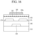
- FIGS. 9 , 10 , 11 , 12 , 13 , 14 , 15 , 16 , 17 , and 18 are cross-sectional views sequentially illustrating an example of a method of manufacturing an organic thin film transistor according to some example embodiments.
- a conductive layer (not shown) is formed on the substrate 110 and then patterned it by photolithography to form a gate electrode 124 .
- the gate insulating film 140 is formed on the whole surface of the substrate 110 including the gate electrode 124 .
- the gate insulating film 140 may be formed of, for example, silicon oxide (SiO 2 ), silicon nitride (SiN x ), aluminum oxide (Al 2 O 3 ), or an organic insulator by, for example, a vapor deposition or a solution process.
- the vapor deposition may be, for example, chemical vapor deposition, vacuum deposition, thermal deposition, or laser deposition and the solution process may be spin coating, screen printing, printing, imprinting, spin casting, dipping, roll coating, drop casting, spray coating, roll printing, slit coating, or inkjet printing, but the present inventive concepts are not limited thereto.
- a conductive layer (not shown) for source and drain electrodes is formed on the gate insulating film 140 and then patterned it by photolithography to form a source electrode 173 and a drain electrode 175 .
- the source electrode 173 and the drain electrode 175 may be formed using a metal mask on the gate insulating film 140 .
- the organic semiconductor thin film 150 is formed on the source electrode 173 and the drain electrode 175 .
- the organic semiconductor thin film 150 may be formed on the whole surface of the substrate 110 , for example, by a vapor deposition or a solution process.
- the organic semiconductor thin film 150 may be formed by coating an organic semiconductor solution prepared by dissolving a low-molecular weight semiconductor, a polymeric semiconductor, or any combination thereof in a solvent through a solution process.
- the solution process may be, for example, spin coating, slit coating, inkjet coating, drop casting, spraying, dipping, or any combination thereof, but is not limited thereto.
- drying and optionally annealing may be performed.
- the annealing may be performed, for example, at about 30° C. to about 200° C. for about 1 minute to about 10 hours, but is not limited thereto.
- a hydrophilic nanolayer 155 is formed on the organic semiconductor thin film 150 .
- the hydrophilic nanolayer 155 may be formed to have a very thin thickness of several nanometers, and may be formed by, for example, a deposition method such as resistance heating deposition, ion beam deposition, or atomic layer deposition or sputtering of an inorganic material, an organic material, an organic-inorganic material, or any combination thereof.
- the hydrophilic nanolayer 155 may be formed of a metal, a metalloid, a metal oxide, a semi-metal oxide, or any combination thereof by vapor deposition such as atomic layer deposition or sputtering.
- vapor deposition or sputtering such as atomic layer deposition may be performed at a relatively low temperature at which the organic semiconductor thin film 150 is not deteriorated, and may be, for example, performed at about 30° C. to about 150° C., but is not limited thereto.
- the sputtering may be performed as low-damage sputtering with little damage to an organic material, but is not limited thereto.
- the hydrophilic nanolayer 155 may be formed on the whole surface or a portion of the organic semiconductor thin film 150 , and when only a portion is formed, for example, a metal mask may be used to form the hydrophilic nanolayer 155 .
- a protective interlayer 160 is formed on the organic semiconductor thin film 150 on which the hydrophilic nanolayer 155 is formed (e.g., the protective interlayer 160 may be formed on the hydrophilic nanolayer 155 ).
- the protective interlayer 160 is to protect the organic semiconductor thin film 150 in a subsequent photolithography process, for example, prevent a chemical liquid used in a subsequent lithography process from directly flowing into the organic semiconductor thin film 150 .
- the protective interlayer 160 may be formed to a relatively thick thickness, and may be formed to a thickness of greater than or equal to about 100 nm, greater than or equal to about 200 nm, greater than or equal to about 300 nm, greater than or equal to about 500 nm, greater than or equal to about 800 nm, or greater than or equal to about 1 ⁇ m, within the above range, about 100 nm to about 10 ⁇ m, about 200 nm to about 10 ⁇ m, about 300 nm to about 10 ⁇ m, about 500 nm to about 10 ⁇ m, about 800 nm to about 10 ⁇ m, or about 1 ⁇ m to about 10 ⁇ m.
- the protective interlayer 160 may include a material different from that of the hydrophilic nanolayer 155 , such that the protective interlayer 160 and the hydrophilic nanolayer 155 may have different total material compositions.
- the protective interlayer 160 may be formed by, for example, coating an aqueous solution containing a water-soluble compound (hereinafter referred to as “aqueous solution for protective interlayer”) by a solution process.
- aqueous solution for protective interlayer a water-soluble compound
- the water-soluble compound may be formed by, for example, coating an aqueous solution prepared by dissolving a water-soluble polymeric compound, a water-soluble low molecular weight compound, or any combination thereof in water, and the water-soluble polymeric compound and/or the water-soluble low molecular weight compound may include one or more hydrophilic functional groups.
- the water-soluble compound may include, for example, poly(ethylene) glycol (PEG), polyvinyl pyrrolidone (PVP), polyvinyl alcohol (PVA), polyacrylic acid (PAA), polyacrylamide, N-(2-hydroxypropyl) methacrylamide, polyoxazoline, polyphosphate, polyphosphazene, xanthan gum, pectin, chitosan, dextran, carrageenan, guar gum, a cellulose ether, a derivative thereof, or any combination thereof, but is not limited thereto.
- the solution process may be, for example, spin coating, slit coating, inkjet coating, drop casting, spraying, dipping, or any combination thereof, but is not limited thereto.
- the hydrophilic nanolayer 155 may serve as an auxiliary layer helping the effective coating of the aqueous solution for the protective interlayer 160 on the organic semiconductor layer 154 , and thus an aqueous solution for the protective interlayer 160 may be effectively coated on the organic semiconductor thin film 150 having a hydrophobic surface.
- drying and optionally annealing may be performed.
- the annealing may be performed, for example, at about 30° C. to about 150° C. for about 1 minute to about 10 hours, but the present inventive concepts are not limited thereto.
- a photoresist film 180 is formed on the protective interlayer 160 .
- the photoresist film 180 may be formed by coating a photoresist solution including a photosensitive material, and may be, for example, a negative photoresist film or a positive photoresist film.
- the photoresist solution may include, for example, a fluorine-containing photoresist, a photoacid generator, and a solvent, and thus the photoresist film 180 may include a fluorine-containing photoresist.
- the fluorine-containing photoresist may implement fine patterning without damaging the organic semiconductor thin film 150 .
- a mask (not shown) is disposed on the photoresist film 180 and exposure is performed.
- the mask may include a light transmitting portion and a light blocking portion, and the light transmitting portion may be disposed at a position corresponding to the region where the photoresist pattern 180 a is to be formed.
- a predetermined region of the photoresist film 180 is selectively exposed and cured by, for example, negative photolithography by irradiating light such as UV, for example, on the mask.
- the photoresist film 180 may include a photoresist pattern 180 a polymerized by exposure and an unexposed portion 180 b.
- various components included in the photoresist film 180 may diffuse downward, and for example, a material such as a photoacid generator included in the photoresist film 180 may flow into the protective interlayer 160 .
- the material diffused downward from the photoresist film 180 in the exposure process may directly flow into the organic semiconductor thin film 150 , and thus, deterioration of electrical characteristics such as a significant change in threshold voltage (Vth) of the organic thin film transistor 100 may be caused.
- Vth threshold voltage
- the protective interlayer 160 is a sacrificial layer removed during the process as described later, even if a material such as a photoacid generator is introduced during exposure, the electrical characteristics of the organic thin film transistor 100 may not be affected.
- the unexposed portion 180 b of the photoresist film 180 is removed by development, leaving only the photoresist pattern 180 a.
- the protective interlayer 160 , the hydrophilic nanolayer 155 and the organic semiconductor thin film 150 are etched using the photoresist pattern 180 a as a mask.
- the etching may be dry etching or wet etching.
- the protective interlayer 160 may be patterned by etching to form the protective interlayer 160 a , and the organic semiconductor thin film 150 may be patterned to form the organic semiconductor layer 154 .
- the photoresist pattern 180 a is removed by stripping, and the patterned protective interlayer 160 a is exposed.
- the protective interlayer 160 a is removed by supplying water. Since the protective interlayer 160 a includes a water-soluble compound as described above, it may be easily removed by dissolving in water, and the hydrophilic nanolayer 155 is not removed because it includes a material insoluble in water as described above. The operations shown in FIGS.
- a photolithography process e.g., a photolithography
- a photolithography process that may be performed on at least the protective interlayer 160 / 160 a , the hydrophilic nanolayer 155 , and the organic semiconductor thin film 154 (restated, a photolithography of at least the protective interlayer 160 / 160 a , the hydrophilic nanolayer 155 , and the organic semiconductor thin film 154 may be performed).
- a photolithography of at least the protective interlayer 160 / 160 a , the hydrophilic nanolayer 155 , and the organic semiconductor thin film 154 may be performed, and then the protective interlayer 160 a may be removed subsequently to performing the photolithography.
- the protective interlayer 160 as a sacrificial layer in the forming of the organic semiconductor layer 154 , materials moving downward from the photoresist film in the photo-etching process (e.g., photolithography process) are prevented from being directly introduced into the organic semiconductor thin film 150 , and thus deterioration of the electrical performance of the organic thin film transistor 100 may be effectively prevented.
- an aqueous solution for the protective interlayer 160 may be effectively coated on the organic semiconductor thin film 150 by forming a very thin hydrophilic nanolayer 155 on the upper surface of the organic semiconductor thin film 150 , and thus, deterioration of the electrical performance of the aforementioned organic thin film transistor 100 may be more effectively prevented.
- the organic thin film transistor 100 shown in FIG. 1 has been described, but the organic thin film transistor 100 shown in FIGS. 2 to 8 is also manufactured substantially by the same manner except in a different order of each layer.
- a styrene-ethylene-butylene-styrene (SEBS) solution obtained by dissolving SEBS and a curing agent in toluene is coated, dried, and photocured to form a stretchable substrate (elongation rate: 700%, elastic modulus: about 1 MPa).
- SEBS styrene-ethylene-butylene-styrene
- Au is formed by a resistance heating deposition on the stretchable substrate to form a gate electrode, and then a SEBS solution containing a curing agent is coated on the gate electrode, photocured, and annealed at 120° C. for 0.5 hours to form a gate insulating film. Then, Au is formed by a resistance heating deposition on the gate insulating film to form a source electrode and a drain electrode.
- Al is formed by resistance heating deposition on the organic semiconductor thin film and then oxidized in air to form a 2 nm-thick hydrophilic nanolayer including aluminum oxide.
- a 10 vol % aqueous solution of Dextran (Aldrich) is coated on the organic semiconductor thin film on which the hydrophilic nanolayer is formed and dried to form a 300 nm-thick protective interlayer.
- a fluorine-based photoresist is coated on the protective interlayer and patterned it by a photolithography to form a fluorine-based photoresist pattern, and the protective interlayer and the organic semiconductor thin film are patterned using the fluorine-based photoresist pattern as a mask to form a patterned protective interlayer and a patterned organic semiconductor layer.
- the fluorine-based photoresist pattern is removed by peeling it off with an isopropyl alcohol-containing fluorine-based solvent (NovecTM, 3M) for 7 minutes, and then spin-coating water on the patterned protective interlayer to dissolve and remove the protective interlayer to manufacture an organic thin film transistor.
- the channel width (W) and channel length (L) of the organic thin film transistor are 1000 ⁇ m and 100 ⁇ m, respectively.
- An organic thin film transistor is manufactured in the same manner as in Example 1, except that the hydrophilic nanolayer and the protective interlayer are not formed.
- An organic thin film transistor is manufactured in the same manner as in Example 1, except that the fluorine-based photoresist is peeled for 21 minutes (three times the peeling time compared to Example 1) without forming the hydrophilic nanolayer and the protective interlayer.
- I SD current value flowing between the source electrode and the drain electrode when a voltage in the range of 20 V to ⁇ 20 V is applied between the gate electrode and the source electrode under the condition of the voltage applied to the source electrode and the drain electrode of 20 V.
- Electrical characteristics are evaluated from the amount of a change or a variation ratio by measuring the reference value (Ref.) before forming the hydrophilic nanolayer and measuring again in the same way after the process is completed.
- the charge mobility of the thin film transistor is obtained from the slope of a graph using (Iso) 1/2 and V G as variables from the saturation region current equation:
- I SD WC 0 2 ⁇ L ⁇ ⁇ ⁇ ( V G ⁇ V T ) 2
- the organic thin film transistor according to Example does not exhibit a significant change in electrical characteristics before and after the process, whereas the organic thin film transistors according to Comparative Examples exhibit significantly deteriorated electrical characteristics.
Landscapes
- Engineering & Computer Science (AREA)
- Manufacturing & Machinery (AREA)
- Thin Film Transistor (AREA)
Abstract
Description

-
- X3 to X9 and X11 to X18 are each independently O, S, Se, or Te,
- X10 is O, S, Se, Te, NRv, CRwRx, or SiRyRz,
- X19 and X20 are NRv, CRwRx, or SiRyRz,
- Ra to Rz are each independently hydrogen, a substituted or unsubstituted C1 to C30 alkyl group, a substituted or unsubstituted C2 to C30 alkenyl group, a substituted or unsubstituted C2 to C30 alkynyl group, a substituted or unsubstituted C3 to C30 cycloalkyl group, a substituted or unsubstituted C3 to C30 cycloalkenyl group, a substituted or unsubstituted C1 to C30 alkoxy group, a substituted or unsubstituted C3 to C30 cycloheteroalkyl group, a substituted or unsubstituted C3 to C30 cycloheteroalkenyl group, a substituted or unsubstituted C6 to C30 aryl group, a substituted or unsubstituted C7 to C30 alkylaryl group, a substituted or unsubstituted C6 to C30 aryloxy group, a substituted or unsubstituted C3 to C30 heterocyclic group, a halogen, a cyano group, or any combination thereof,
- n is 0, 1, or 2, and
- * is a linking point of the polymer backbone.

-
- R4 and R5 may each independently be hydrogen, a substituted or unsubstituted C1 to C30 alkyl group, a substituted or unsubstituted C1 to C30 alkoxy group, a substituted or unsubstituted C2 to C30 alkoxyalkyl group, a substituted or unsubstituted C6 to C30 aryl group, —CORd, —OCORe, —COORf, —OCOORg, a halogen, a cyano group, or any combination thereof,
- Rd to Rg may each independently be hydrogen, a substituted or unsubstituted C1 to C30 alkyl group, a substituted or unsubstituted C1 to C30 alkoxy group, a substituted or unsubstituted C2 to C30 alkoxyalkyl group, a substituted or unsubstituted C6 to C30 aryl group, a halogen, a cyano group, or any combination thereof, and
- * may be a linking point of the polymer backbone.
-
- wherein ISD is the source-drain current, μ or μFET is the charge mobility, C0 is a capacitance of the gate insulating film, W is a channel width, L is a channel length, VG is a gate voltage, and VT is a threshold voltage. Herein, the voltage at which a straight line extrapolated from the maximum slope region of the (ISD)1/2-VG graph intersects the VG axis is VT.
| TABLE 1 | |||
| Change of threshold | Variation ratio of | ||
| voltage | charge mobility | ||
| (V) | (%) | ||
| Example 1 | +0.72 | −3 | ||
| Comparative | +11.66 | +1 | ||
| Example 1 | ||||
| Comparative | +0.78 | −32 | ||
| Example 2 | ||||
| * Change of threshold voltage: Change of threshold voltage relative to Ref. after the process is completed. | ||||
| * Variation ratio of charge mobility: Variation ratio of charge mobility relative to Ref. after the process is completed. | ||||
Claims (8)
Applications Claiming Priority (2)
| Application Number | Priority Date | Filing Date | Title |
|---|---|---|---|
| KR1020210140946A KR20230057017A (en) | 2021-10-21 | 2021-10-21 | Organic thin film transistor and method of manufacturing the same and thin film transistor array panel and electronic device |
| KR10-2021-0140946 | 2021-10-21 |
Publications (2)
| Publication Number | Publication Date |
|---|---|
| US20230131263A1 US20230131263A1 (en) | 2023-04-27 |
| US12317666B2 true US12317666B2 (en) | 2025-05-27 |
Family
ID=86055758
Family Applications (1)
| Application Number | Title | Priority Date | Filing Date |
|---|---|---|---|
| US17/678,453 Active 2043-07-27 US12317666B2 (en) | 2021-10-21 | 2022-02-23 | Organic thin film transistor and method of manufacturing the same and thin film transistor array panel and electronic device |
Country Status (2)
| Country | Link |
|---|---|
| US (1) | US12317666B2 (en) |
| KR (1) | KR20230057017A (en) |
Families Citing this family (1)
| Publication number | Priority date | Publication date | Assignee | Title |
|---|---|---|---|---|
| KR102780630B1 (en) * | 2023-06-28 | 2025-03-12 | 고려대학교 산학협력단 | Metal oxide thin film transistor with multilayer channel structure and fabrication method thereof |
Citations (29)
| Publication number | Priority date | Publication date | Assignee | Title |
|---|---|---|---|---|
| US20030157432A1 (en) * | 2002-01-31 | 2003-08-21 | Jorg Rottstegge | Fluorine-containing photoresist having reactive anchors for chemical amplification and improved copolymerization properties |
| JP2008071781A (en) | 2006-09-12 | 2008-03-27 | Sony Corp | Manufacturing method of semiconductor device |
| KR20100068749A (en) | 2008-12-15 | 2010-06-24 | 한국전자통신연구원 | The manufacturing method of transistor for bio sensor |
| US20100200844A1 (en) * | 2009-02-10 | 2010-08-12 | Industrial Technology Research Institute | Organic thin film transistor and fabricating method thereof |
| US20100264408A1 (en) * | 2007-11-20 | 2010-10-21 | Cambridge Display Technology Ltd. | Organic Thin Film Transistors, Active Matrix Organic Optical Devices and Methods of Making the Same |
| US7939453B2 (en) | 2008-02-29 | 2011-05-10 | Dai Nippon Printing Co., Ltd. | Method for manufacturing organic transistor and organic transistor |
| US20120273786A1 (en) | 2009-10-27 | 2012-11-01 | Sumitomo Chemical Company, Limited | Organic surface protective layer composition and method for protecting organic surface |
| US20150070422A1 (en) * | 2013-09-06 | 2015-03-12 | Canon Finetech Inc. | Recording head for ink jet recording, ink jet recording apparatus, and ink jet recording method |
| KR20150052763A (en) | 2013-11-06 | 2015-05-14 | 삼성전자주식회사 | Thin film transistor and method of manufacturing the same and electronic device including the thin film transistor |
| US9401487B2 (en) | 2012-11-12 | 2016-07-26 | Samsung Electronics Co., Ltd. | Channel layer for stretchable transistors |
| US9478727B2 (en) | 2012-03-12 | 2016-10-25 | Fraunhofer-Gesellschaft zur Förderung der angewandten Forschung e.V. | Fluorosilicone-based dielectric elastomer and method for its production |
| US20160365247A1 (en) * | 2015-06-11 | 2016-12-15 | Incheon University Industry Academic Cooperation Foundation | Method of fabricating transient semiconductor based on single-wall nanotube |
| US20170224257A1 (en) | 2014-08-11 | 2017-08-10 | The Board Of Trustees Of The University Of Lllinois | Epidermal Photonic Systems and Methods |
| US9799708B2 (en) | 2015-03-10 | 2017-10-24 | Samsung Display Co., Ltd. | Organic light emitting diode display |
| US20170331045A1 (en) | 2016-05-12 | 2017-11-16 | Samsung Electronics Co., Ltd. | Organic semiconductor thin film and method of manufacturing the same and thin film transistor and electronic device |
| US9887373B2 (en) | 2013-11-06 | 2018-02-06 | Samsung Electronics Co., Ltd. | Thin film transistor, method of manufacturing the same, and electronic device including the thin film transistor |
| US9945739B2 (en) | 2015-05-29 | 2018-04-17 | Korea University Research And Business Foundation | Flexible pressure sensor using amorphous metal and flexible bimodal sensor for simultaneously sensing pressure and temperature |
| US20190244064A1 (en) * | 2016-10-25 | 2019-08-08 | Nec Corporation | Pattern recognition apparatus, method and medium |
| US10417948B2 (en) | 2016-02-25 | 2019-09-17 | Samsung Display Co., Ltd. | Stretchable display device |
| US20190333942A1 (en) * | 2016-04-12 | 2019-10-31 | Semiconductor Energy Laboratory Co., Ltd. | Peeling method and manufacturing method of flexible device |
| US20190372037A1 (en) * | 2018-06-01 | 2019-12-05 | Samsung Electronics Co., Ltd. | Thin film transistor and method of manufacturing the same and thin film transistor panel and electronic device |
| US20200044089A1 (en) * | 2018-08-03 | 2020-02-06 | Shenzhen China Star Optoelectronics Technology Co., Ltd. | Oxide semiconductor thin film transistor and manufacturing method thereof |
| US20210036229A1 (en) | 2019-07-30 | 2021-02-04 | Samsung Electronics Co., Ltd. | Polymer and organic thin film and thin film transistor and electronic device |
| KR20210014566A (en) | 2019-07-30 | 2021-02-09 | 삼성전자주식회사 | Polymer and organic thin film and thin film transistor and electronic device |
| US20210151680A1 (en) * | 2017-07-04 | 2021-05-20 | Sumitomo Chemical Company, Limited | Organic thin-film transistor and polymer compound |
| US20210184165A1 (en) * | 2018-12-04 | 2021-06-17 | Wuhan China Star Optoelectronics Semiconductor Display Technology Co., Ltd. | Flexible oled display device |
| US20210225660A1 (en) * | 2020-01-17 | 2021-07-22 | Taiwan Semiconductor Manufacturing Company, Ltd. | Semiconductor Device and Method of Manufacture |
| US20210296599A1 (en) | 2020-03-17 | 2021-09-23 | Samsung Electronics Co., Ltd. | Stretchable devices, display panels, sensors, and electronic devices |
| US20210305286A1 (en) * | 2019-11-21 | 2021-09-30 | Chongqing Konka Photoelectric Technology Research Institute Co., Ltd. | Tft, method for manufacturing the same, and tft array |
-
2021
- 2021-10-21 KR KR1020210140946A patent/KR20230057017A/en active Pending
-
2022
- 2022-02-23 US US17/678,453 patent/US12317666B2/en active Active
Patent Citations (31)
| Publication number | Priority date | Publication date | Assignee | Title |
|---|---|---|---|---|
| US20030157432A1 (en) * | 2002-01-31 | 2003-08-21 | Jorg Rottstegge | Fluorine-containing photoresist having reactive anchors for chemical amplification and improved copolymerization properties |
| JP2008071781A (en) | 2006-09-12 | 2008-03-27 | Sony Corp | Manufacturing method of semiconductor device |
| US20100264408A1 (en) * | 2007-11-20 | 2010-10-21 | Cambridge Display Technology Ltd. | Organic Thin Film Transistors, Active Matrix Organic Optical Devices and Methods of Making the Same |
| JP5360737B2 (en) | 2008-02-29 | 2013-12-04 | 大日本印刷株式会社 | Organic transistor manufacturing method and organic transistor |
| US7939453B2 (en) | 2008-02-29 | 2011-05-10 | Dai Nippon Printing Co., Ltd. | Method for manufacturing organic transistor and organic transistor |
| KR20100068749A (en) | 2008-12-15 | 2010-06-24 | 한국전자통신연구원 | The manufacturing method of transistor for bio sensor |
| US20100200844A1 (en) * | 2009-02-10 | 2010-08-12 | Industrial Technology Research Institute | Organic thin film transistor and fabricating method thereof |
| US20120273786A1 (en) | 2009-10-27 | 2012-11-01 | Sumitomo Chemical Company, Limited | Organic surface protective layer composition and method for protecting organic surface |
| US9478727B2 (en) | 2012-03-12 | 2016-10-25 | Fraunhofer-Gesellschaft zur Förderung der angewandten Forschung e.V. | Fluorosilicone-based dielectric elastomer and method for its production |
| US9401487B2 (en) | 2012-11-12 | 2016-07-26 | Samsung Electronics Co., Ltd. | Channel layer for stretchable transistors |
| US20150070422A1 (en) * | 2013-09-06 | 2015-03-12 | Canon Finetech Inc. | Recording head for ink jet recording, ink jet recording apparatus, and ink jet recording method |
| KR20150052763A (en) | 2013-11-06 | 2015-05-14 | 삼성전자주식회사 | Thin film transistor and method of manufacturing the same and electronic device including the thin film transistor |
| US9887373B2 (en) | 2013-11-06 | 2018-02-06 | Samsung Electronics Co., Ltd. | Thin film transistor, method of manufacturing the same, and electronic device including the thin film transistor |
| US20170224257A1 (en) | 2014-08-11 | 2017-08-10 | The Board Of Trustees Of The University Of Lllinois | Epidermal Photonic Systems and Methods |
| US9799708B2 (en) | 2015-03-10 | 2017-10-24 | Samsung Display Co., Ltd. | Organic light emitting diode display |
| US9945739B2 (en) | 2015-05-29 | 2018-04-17 | Korea University Research And Business Foundation | Flexible pressure sensor using amorphous metal and flexible bimodal sensor for simultaneously sensing pressure and temperature |
| US20160365247A1 (en) * | 2015-06-11 | 2016-12-15 | Incheon University Industry Academic Cooperation Foundation | Method of fabricating transient semiconductor based on single-wall nanotube |
| US10417948B2 (en) | 2016-02-25 | 2019-09-17 | Samsung Display Co., Ltd. | Stretchable display device |
| US20190333942A1 (en) * | 2016-04-12 | 2019-10-31 | Semiconductor Energy Laboratory Co., Ltd. | Peeling method and manufacturing method of flexible device |
| US20170331045A1 (en) | 2016-05-12 | 2017-11-16 | Samsung Electronics Co., Ltd. | Organic semiconductor thin film and method of manufacturing the same and thin film transistor and electronic device |
| US20190244064A1 (en) * | 2016-10-25 | 2019-08-08 | Nec Corporation | Pattern recognition apparatus, method and medium |
| US20210151680A1 (en) * | 2017-07-04 | 2021-05-20 | Sumitomo Chemical Company, Limited | Organic thin-film transistor and polymer compound |
| US20190372037A1 (en) * | 2018-06-01 | 2019-12-05 | Samsung Electronics Co., Ltd. | Thin film transistor and method of manufacturing the same and thin film transistor panel and electronic device |
| US20200044089A1 (en) * | 2018-08-03 | 2020-02-06 | Shenzhen China Star Optoelectronics Technology Co., Ltd. | Oxide semiconductor thin film transistor and manufacturing method thereof |
| US20210184165A1 (en) * | 2018-12-04 | 2021-06-17 | Wuhan China Star Optoelectronics Semiconductor Display Technology Co., Ltd. | Flexible oled display device |
| US20210036229A1 (en) | 2019-07-30 | 2021-02-04 | Samsung Electronics Co., Ltd. | Polymer and organic thin film and thin film transistor and electronic device |
| KR20210014566A (en) | 2019-07-30 | 2021-02-09 | 삼성전자주식회사 | Polymer and organic thin film and thin film transistor and electronic device |
| US20210305286A1 (en) * | 2019-11-21 | 2021-09-30 | Chongqing Konka Photoelectric Technology Research Institute Co., Ltd. | Tft, method for manufacturing the same, and tft array |
| US20210225660A1 (en) * | 2020-01-17 | 2021-07-22 | Taiwan Semiconductor Manufacturing Company, Ltd. | Semiconductor Device and Method of Manufacture |
| US20210296599A1 (en) | 2020-03-17 | 2021-09-23 | Samsung Electronics Co., Ltd. | Stretchable devices, display panels, sensors, and electronic devices |
| KR20210116061A (en) | 2020-03-17 | 2021-09-27 | 삼성전자주식회사 | Stretchable device and display panel and sensor and electronic device |
Also Published As
| Publication number | Publication date |
|---|---|
| KR20230057017A (en) | 2023-04-28 |
| US20230131263A1 (en) | 2023-04-27 |
Similar Documents
| Publication | Publication Date | Title |
|---|---|---|
| US8039296B2 (en) | Organic thin film transistor array panel and manufacturing method thereof | |
| US7834352B2 (en) | Method of fabricating thin film transistor | |
| US8253137B2 (en) | Laminate structure, electronic device, and display device | |
| US20070024766A1 (en) | Organic thin film transistor display panel | |
| EP1865558A2 (en) | Thin film transistor array panel and method of manufacturing the same | |
| US20080258138A1 (en) | Thin film transistor array panel and fabricating method thereof, and flat panel display with the same | |
| CN102738393A (en) | Thin-film device, method of manufacturing the same, and method of manufacturing image display apparatus | |
| US9887373B2 (en) | Thin film transistor, method of manufacturing the same, and electronic device including the thin film transistor | |
| JP2007251093A (en) | Gate insulating film, organic thin film transistor, method for producing the transistor, and display device | |
| EP3435435B1 (en) | Thin film transistor and method of manufacturing the same | |
| US12317666B2 (en) | Organic thin film transistor and method of manufacturing the same and thin film transistor array panel and electronic device | |
| US9761818B2 (en) | Method of manufacturing thin film transistor, thin film transistor manufactured by the method, and electronic device comprising the thin film transistor | |
| JP2006005352A (en) | Thin film transistor array panel using organic semiconductor and manufacturing method thereof | |
| CN100563021C (en) | Organic thin film transistor array panel and manufacturing method thereof | |
| CN100463248C (en) | Manufacturing method of organic light emitting display and display manufactured by the method | |
| US20070278492A1 (en) | Thin film transistor array panel and method of manufacturing the same | |
| KR20100122915A (en) | Method of fabricating top gate organic semiconductor transistors | |
| KR102277814B1 (en) | Thin film transistor and method of manufacturing the same and electronic device including the thin film transistor | |
| US20180123064A1 (en) | Method of manufacturing thin film transistor, thin film transistor, and electronic device comprising the thin film transistor | |
| US9018622B2 (en) | Method for manufacturing organic semiconductor element | |
| JPWO2006129718A1 (en) | Organic thin film transistor | |
| US20060202200A1 (en) | Organic thin film transistor array panel and manufacturing method thereof | |
| US9484542B2 (en) | Thin film transistor panel and method of manufacturing the same, and electronic device including the thin film transistor panel | |
| JP2006148114A (en) | Thin film transistor array panel using semiconductor and manufacturing method thereof | |
| JP2020088117A (en) | Thin film transistor array substrate, image display device substrate, image display device, and manufacturing method thereof |
Legal Events
| Date | Code | Title | Description |
|---|---|---|---|
| FEPP | Fee payment procedure |
Free format text: ENTITY STATUS SET TO UNDISCOUNTED (ORIGINAL EVENT CODE: BIG.); ENTITY STATUS OF PATENT OWNER: LARGE ENTITY |
|
| AS | Assignment |
Owner name: SAMSUNG ELECTRONICS CO., LTD., KOREA, REPUBLIC OF Free format text: ASSIGNMENT OF ASSIGNORS INTEREST;ASSIGNORS:KUZUMOTO, YASUTAKA;HAHM, SUK GYU;CHUNG, JONG WON;AND OTHERS;REEL/FRAME:059128/0657 Effective date: 20220210 |
|
| STPP | Information on status: patent application and granting procedure in general |
Free format text: DOCKETED NEW CASE - READY FOR EXAMINATION |
|
| STPP | Information on status: patent application and granting procedure in general |
Free format text: NON FINAL ACTION MAILED |
|
| STPP | Information on status: patent application and granting procedure in general |
Free format text: RESPONSE TO NON-FINAL OFFICE ACTION ENTERED AND FORWARDED TO EXAMINER |
|
| STPP | Information on status: patent application and granting procedure in general |
Free format text: NOTICE OF ALLOWANCE MAILED -- APPLICATION RECEIVED IN OFFICE OF PUBLICATIONS |
|
| STPP | Information on status: patent application and granting procedure in general |
Free format text: AWAITING TC RESP., ISSUE FEE NOT PAID |
|
| STPP | Information on status: patent application and granting procedure in general |
Free format text: NOTICE OF ALLOWANCE MAILED -- APPLICATION RECEIVED IN OFFICE OF PUBLICATIONS |
|
| STCF | Information on status: patent grant |
Free format text: PATENTED CASE |