CROSS-REFERENCE TO RELATED APPLICATIONS
This is a continuation of International Patent Application No. PCT/CN2022/078211, filed on Feb. 28, 2022, which claims the priority to Chinese Patent Application No. 202210054173.6, titled “MEMORY DEVICE, AND MANUFACTURING METHOD AND DRIVING METHOD THEREOF” and filed on Jan. 18, 2022. The entire contents of International Patent Application No. PCT/CN2022/078211 and Chinese Patent Application No. 202210054173.6 are incorporated herein by reference.
TECHNICAL FIELD
The present disclosure relates to the technical field of semiconductor manufacturing, and in particular, to a memory device, and a manufacturing method and a driving method thereof.
BACKGROUND
As a semiconductor device commonly used in an electronic device such as a computer, a dynamic random access memory (DRAM) includes a plurality of memory cells, and each of the memory cells usually includes a transistor and a capacitor. The transistor has a gate electrically connected to a word line, a source electrically connected to a bit line, and a drain electrically connected to the capacitor. A word line voltage on the word line can control on and off of the transistor, such that data information stored in the capacitor can be read through the bit line or data information can be written into the capacitor through the bit line.
However, with the rapid development of the semiconductor industry, semiconductor enterprises want to maximize benefits, and consumers expect to realize multi-function semiconductor products. However, existing memory devices have single functions due to limitations on their structures.
Therefore, how to realize a function of a memory device to expand an application field of the memory device is an urgent technical problem to be resolved.
SUMMARY
According to some embodiments, the present disclosure provides a memory device, including:
-
- a substrate;
- a stacked structure, where the stacked structure includes a first gate layer, a second gate layer, and interlayer isolation layers, one of the interlayer isolation layers is located between the first gate layer and the second gate layer, and another one of the interlayer isolation layers is located between the first gate layer and the substrate; and
- a memory structure, including a through hole penetrating through the stacked structure, and a trench structure filled in the through hole.
According to some other embodiments, the present disclosure further provides a manufacturing method of a memory device, including the following steps:
-
- providing a substrate;
- forming a stacked layer, where the stacked layer includes a first interlayer isolation layer, a sacrificial layer, a second interlayer isolation layer, and a second gate layer that are successively stacked on the substrate;
- etching the stacked layer to form a through hole penetrating through the stacked layer;
- forming a trench structure in the through hole; and
- removing the sacrificial layer and replacing the sacrificial layer with a conductive material to form a first gate layer.
According to some other embodiments, the present disclosure further provides a driving method of the memory device described above, including the following steps:
-
- in a first storage mode, applying a first turn-on voltage to the second gate layer and applying a first storage voltage to the first gate layer, to write information into the ferroelectric layer; and
- in a second storage mode, applying a second turn-on voltage to the second gate layer and applying a second storage voltage to the first gate layer, to write information into the charge capture layer.
BRIEF DESCRIPTION OF THE DRAWINGS
FIG. 1A is a schematic cross-sectional view of a memory device according to a specific implementation of the present disclosure;
FIG. 1B is a schematic cross-sectional view of a trench structure according to a specific implementation of the present disclosure;
FIG. 2 is a schematic principle diagram when a memory device is used as a ferroelectric memory according to a specific implementation of the present disclosure;
FIG. 3 is a schematic principle diagram when a memory device is used as a flash memory according to a specific implementation of the present disclosure;
FIG. 4 is a schematic diagram of a three-dimensional structure of a memory device according to a specific implementation of the present disclosure;
FIG. 5 is a flowchart of a manufacturing method of a memory device according to a specific implementation of the present disclosure;
FIG. 6A to FIG. 6P are schematic cross-sectional views of main processing steps along a first direction during manufacturing of a memory device according to a specific implementation of the present disclosure;
FIG. 7A to FIG. 7P are schematic cross-sectional views of main processing steps along a second direction during manufacturing of a memory device according to a specific implementation of the present disclosure; and
FIG. 8 is a flowchart of a driving method of a memory device according to a specific implementation of the present disclosure.
DETAILED DESCRIPTION
Specific implementations of a memory device, and a manufacturing method and a driving method thereof provided in the present disclosure will be described below in detail with reference to the accompanying drawings.
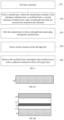
The specific implementations of the present disclosure provide a memory device. FIG. 1A is a schematic cross-sectional view of the memory device according to a specific implementation of the present disclosure. FIG. 1B is a schematic cross-sectional view of a trench structure according to a specific implementation of the present disclosure. FIG. 2 is a schematic principle diagram when the memory device is used as a ferroelectric memory according to a specific implementation of the present disclosure. FIG. 3 is a schematic principle diagram when the memory device is used as a flash memory according to a specific implementation of the present disclosure. FIG. 4 is a schematic diagram of a three-dimensional structure of the memory device according to a specific implementation of the present disclosure. As shown in FIG. 1A, FIG. 1B, and FIG. 2 to FIG. 4 , the memory device includes:
-
- a substrate 10;
- a stacked structure 11, where the stacked structure 11 includes a first gate layer 112, a second gate layer 114, and interlayer isolation layers, one of the interlayer isolation layers is located between the first gate layer 112 and the second gate layer 114, and another one of the interlayer isolation layers is located between the first gate layer 112 and the substrate 10; and
- a memory structure 12, including a through hole penetrating through the stacked structure 11, and a trench structure filled in the through hole.
Specifically, the substrate 10 may be but not limited to a silicon substrate. This specific implementation is described by taking the substrate as the silicon substrate for example. In other embodiments, the substrate 10 may alternatively be a semiconductor substrate such as a gallium nitride substrate, a gallium arsenide substrate, a gallium carbide substrate, a silicon carbide substrate or a silicon-on-insulator (SOI) substrate. The interlayer isolation layer includes a first interlayer isolation layer 111 between the first gate layer 112 and the substrate 10, and a second interlayer isolation layer 113 between the first gate layer 112 and the second gate layer 114. A top surface of the through hole is flush with a top surface of the stacked structure 11 (namely, a top surface of the second gate layer 114 in the stacked structure 11). When the memory device is used to store information, the trench structure connected to the first gate layer 112 can be turned on by applying a turn-on voltage to the second gate layer 114. Then, the information is written by applying a storage voltage to the first gate layer 112. The information can be stored in different regions of the trench structure by adjusting the storage voltage applied to the first gate layer 112. In this way, the memory device can be used as a ferroelectric memory (such as an FeRAM) or a flash memory (such as an NAND), in other words, the memory device can work in two different storage modes, so as to realize versatility of the memory device and expand an application field of the memory device.
In some embodiments, the trench structure includes a tunneling layer 121 covering an inner wall of the through hole, a charge capture layer 122 covering a surface of the tunneling layer 121, a ferroelectric layer 123 covering a surface of the charge capture layer 122, a buffer layer 124 covering a surface of the ferroelectric layer 123, and a channel layer 125 covering a surface of the buffer layer 124.
Specifically, the tunneling layer 121, the charge capture layer 122, the ferroelectric layer 123, the buffer layer 124, and the channel layer 125 are successively stacked along a direction in which the inner wall of the through hole points to a center of the through hole. The material of the tunneling layer 121 may be an oxide material, for example, silicon dioxide. The material of the charge capture layer 122 may be a silicon oxynitride material, a silicon nitride material, a silicon oxide composite material, or a high-K dielectric composite material. In an embodiment, the material of the charge capture layer 122 is a zinc silicon oxide (ZSO) material. The material of the ferroelectric layer 123 may be a hafnium oxide material, a zirconium oxide material, a lead zirconate titanate material, or a hafnium zirconium oxide (HZO) material. In an embodiment, the material of the ferroelectric layer 123 is a hafnium zirconium oxide material. The material of the buffer layer 124 may be the oxide material, for example, silicon dioxide. The material of the channel layer 125 may be a polycrystalline silicon material, a silicon germanium (SiGe) material, or an indium gallium zinc oxide (IGZO) material. In an embodiment, the material of the channel layer 125 is the polycrystalline silicon material.
As shown in FIG. 2 , when the memory device provided in this specific implementation is used as a nonvolatile memory such as the FeRAM, during a write operation, after a first turn-on voltage is applied to the second gate layer 114, a first storage voltage is applied to the first gate layer 112 to polarize the ferroelectric layer 123. After the polarization, a charge is generated on the surface of the ferroelectric layer 123, so as to write the information. During a read operation, a turn-on voltage of the trench structure where the ferroelectric layer 123 is polarized decreases. In this case, a first reading voltage is applied to the first gate layer 112, such that an S/D circuit corresponding to the trench structure is turned on and a number 1 is read. For the trench structure where the ferroelectric layer 123 is not polarized, the first reading voltage is applied to the first gate layer 112, such that the S/D circuit corresponding to the trench structure is turned off and a number 0 is read. During an erasing operation, a first erasing voltage is applied to the first gate layer 112 to perform depolarization by using a measured ferroelectric hysteresis loop of the ferroelectric layer 123, so as to erase the information stored in the memory device. The substrate 10 in FIG. 2 further includes a source region 101 and a drain region 102.
As shown in FIG. 3 , when the memory device provided in this specific implementation is used as the nonvolatile memory such as the NAND, during the write operation, after a second turn-on voltage is applied to the second gate layer 114, a second storage voltage greater than the first storage voltage is applied to the first gate layer 112, such that an electron or a hole enters the charge capture layer 122 after passing through the tunneling layer 121 and are stored in the charge capture layer 122. The electron stored in the charge capture layer 122 enables the polarization of the ferroelectric layer 123 to be preserved for a long time, so as to realize a nonvolatile storage function of the memory device. During the read operation, the turn-on voltage of the trench structure where the ferroelectric layer 123 is polarized decreases. In this case, a second reading voltage is applied to the first gate layer 112, such that the S/D circuit corresponding to the trench structure is turned on and the number 1 is read. For the trench structure where the ferroelectric layer 123 is not polarized, the second reading voltage is applied to the first gate layer 112, such that the S/D circuit corresponding to the trench structure is turned off and the number 0 is read. During the erasing operation, a second erasing voltage is applied to the first gate layer 112 to perform depolarization by using the measured ferroelectric hysteresis loop of the ferroelectric layer 123 so as to erase the information stored in the memory device. The substrate 10 in FIG. 2 further includes a source region 101 and a drain region 102.
In some embodiments, the channel layer 125 penetrates through the tunneling layer 121, the charge capture layer 122, the ferroelectric layer 123, and the buffer layer 124, which are at the bottom of the through hole; and a bottom surface of the channel layer 125 comes into contact with the substrate 10; and the memory device further includes:
-
- a drain 14, where the drain 14 is connected to a top surface of the channel layer 125 in a contact manner.
In some embodiments, the trench structure further covers the top surface of the stacked structure 11; and
-
- the drain 14 penetrates through the trench structure located on the top surface of the stacked structure 11.
Specifically, the bottom surface of the channel layer 125 is connected to the source region inside the substrate 10 in the contact manner, and the top surface of the channel layer 125 is connected to the drain 14 in the contact manner. The memory device further includes a first coating layer 13 covering the trench structure on the top surface of the stacked structure 11 to avoid damage caused by a subsequent process to the trench structure, especially the channel layer 125 in the trench structure. The drain 14 passes through, along a direction perpendicular to a top surface of the substrate 10 (for example, a Z-axis direction in FIG. 1A), the first coating layer 13 and the trench structure on the top surface of the stacked structure 11, so as to facilitate subsequent lead-out of a contact point of the drain 14. The memory device further includes a second coating layer 15 that covers the first coating layer 13 and the drain 14. The material of the first coating layer 13 may be the oxide material (such as silicon dioxide), and the material of the second coating layer 15 may be a nitride material (such as silicon nitride).
In some embodiments, a plurality of memory structures 12 are arranged in an array along a first direction and a second direction, to increase storage density of the memory device.
In some embodiments, the first gate layer 112 includes a plurality of first gate structures 40 that are parallel spaced along the second direction, the second gate layer 114 includes a plurality of second gate structures 41 that are parallel spaced along the second direction, the plurality of second gate structures 41 are located above the plurality of first gate structures 40; and a plurality of memory structures 12, that are arranged in parallel along the first direction share the plurality of first gate structures 40 and the plurality of second gate structures 41.
In some embodiments, the memory device further includes:
-
- a separation structure 16, where the separation structure 16 penetrates through the stacked structure 11 along the direction perpendicular to the top surface of the substrate 10 and is located between two adjacent ones of the plurality of first gate structures 40 and between two adjacent ones of the plurality of second gate structures 41.
The following provides description by using an example in which an X-axis direction in FIG. 4 is the first direction and a Y-axis direction in FIG. 4 is the second direction, the X-axis direction is perpendicular to the Y-axis direction, and a Z-axis direction is perpendicular to the Y-axis direction. For example, as shown in FIG. 1A and FIG. 4 , the memory device includes a plurality of memory structures 12 that are arranged in a two-dimensional array along the X-axis direction and the Y-axis direction. The separation structure 16 penetrates through the stacked structure 11 along the Z-axis direction. Each separation structure 16 extends along the X-axis direction, and a plurality of separation structures 16 are arranged in parallel along the Y-axis direction to separate the first gate layer 112 into the plurality of first gate structures 40 that are parallel spaced along the Y-axis direction and the second gate layer 114 into the plurality of second gate structures 41 that are parallel spaced along the Y-axis direction. Each of the plurality of first gate structures 40 and each of the plurality of second gate structures 41 extend along the X-axis direction. The material of the separation structure 16 is an insulating material such as silicon dioxide, to electrically isolate two adjacent ones of the plurality of first gate structures 40 and two adjacent ones of the plurality of second gate structures 41.
In some embodiments, the material of the first gate structure 40 is a metallic material, and the material of the second gate structure 41 is the polycrystalline silicon material.
For example, the first gate structure 40 may be made of, but not limited to, tungsten. One of the plurality of second gate structures 41 is configured to turn on all of the plurality of memory structures 12 arranged along the first direction. Since the second gate structure 41 is closer to a top metal layer of the memory device than the first gate structure 40, a turn-on voltage of the second gate structure 41 is greatly different from that of the first gate structure 40 due to impact of an electric field of the top metal layer. Therefore, the material of the first gate structure 40 and the material of the second gate structure 41 are different, so as to apply different voltages to the first gate structure 40 and the second gate structure 41. The top metal layer is a metal layer for transmitting a control signal from the outside to the memory structure 12.
According to some other embodiments, the specific implementations further provide a manufacturing method of a memory device. FIG. 5 is a flowchart of a manufacturing method of a memory device according to a specific implementation of the present disclosure. FIG. 6A to FIG. 6P are schematic cross-sectional views of main processing steps along a first direction during manufacturing of the memory device according to a specific implementation of the present disclosure. FIG. 7A to FIG. 7P are schematic cross-sectional views of main processing steps along a second direction during manufacturing of the memory device according to a specific implementation of the present disclosure. For schematic structural diagrams of a memory device manufactured in this specific implementation, reference may be made to FIG. 1A, FIG. 1B, and FIG. 2 to FIG. 4 . As shown in FIG. 4 , FIG. 5 , FIG. 6A to 6P, and FIG. 7A to FIG. 7P, the manufacturing method of a memory device includes the following steps:
Step S51: Provide a substrate 10, as shown in FIG. 6A and FIG. 7A.
Step S52: Form a stacked layer, where the stacked layer includes a first interlayer isolation layer 111, a sacrificial layer 60, a second interlayer isolation layer 113, and a second gate layer 114 that are successively stacked on the substrate 10, as shown in FIG. 6B and FIG. 7B.
Specifically, the substrate 10 may be but not limited to a silicon substrate. This specific implementation is described by taking the substrate as the silicon substrate for example. In other embodiments, the substrate 10 may alternatively be a semiconductor substrate such as a gallium nitride substrate, a gallium arsenide substrate, a gallium carbide substrate, a silicon carbide substrate or an SOI substrate. There should be a large etch selectivity of the sacrificial layer 60 to the first interlayer isolation layer 111 and a large etch selectivity of the sacrificial layer 60 to the second interlayer isolation layer 113 to facilitate subsequent selective removal of the sacrificial layer 60. In an example, both the etch selectivity of the sacrificial layer 60 to the first interlayer isolation layer 111 and the etch selectivity of the sacrificial layer 60 to the second interlayer isolation layer 113 are greater than 3. In an embodiment, the materials of the first interlayer isolation layer 111 and the second interlayer isolation layer 113 may be oxide materials (for example, silicon dioxide), and the material of the sacrificial layer 60 may be a nitride material (for example, silicon nitride). The material of the second gate layer 114 may be a polycrystalline silicon material.
Step S53: Etch the stacked layer to form a through hole 61 penetrating through the stacked layer, as shown in FIG. 6C and FIG. 7C.
In some embodiments, the forming a through hole 61 penetrating through the stacked layer specifically includes:
-
- etching the stacked layer to form a plurality of through holes 61 each penetrating through the stacked layer, wherein the plurality of through holes 61 are arranged in an array along a first direction and a second direction, where the first direction and the second direction are parallel to a top surface of the substrate 10, and the first direction intersects with the second direction.
Specifically, the stacked layer can be etched through dry etching along a direction perpendicular to the top surface of the substrate 10 to form the plurality of through holes 61 arranged in a two-dimensional array along the first direction and the second direction, and each of the plurality of through holes 61 penetrates through the stacked layer along the direction perpendicular to the top surface of the substrate 10. The first direction and the second direction may be intersected vertically or obliquely. This specific implementation is described by taking vertical intersection of the first direction and the second direction as an example.
Step S54: Form a trench structure in the through hole 61, as shown in FIG. 6I and FIG. 7I.
In some embodiments, the trench structure may include a tunneling layer 121 covering an inner wall of the through hole, a charge capture layer 122 covering a surface of the tunneling layer 121, a ferroelectric layer 123 covering a surface of the charge capture layer 122, a buffer layer 124 covering a surface of the ferroelectric layer 123, and a channel layer 125 covering a surface of the buffer layer 124.
In some embodiments, the forming a trench structure in the through hole 61 specifically includes:
-
- forming the tunneling layer 121 on the inner wall of the through hole 61 and a top surface of the stacked layer, as shown in FIG. 6D and FIG. 7D;
- forming the charge capture layer 122 on the surface of the tunneling layer 121;
- forming the ferroelectric layer 123 on the surface of the charge capture layer 122, as shown in FIG. 6E and FIG. 7E;
- forming the buffer layer 124 on the surface of the ferroelectric layer 123, as shown in FIG. 6F and FIG. 7F; and
- forming the channel layer 125 on the surface of the buffer layer 124, as shown in FIG. 6I and FIG. 7I.
In some embodiments, the forming the channel layer 125 on the surface of the buffer layer 124 specifically includes:
-
- etching the buffer layer 124, the ferroelectric layer 123, the charge capture layer 122, and the tunneling layer 121, which are at the bottom of the through hole 61, to form a penetrating hole exposing the substrate 10, as shown in FIG. 6H and FIG. 7H; and
- forming the channel layer 125 that fills up the penetrating hole and covers the surface of the buffer layer 124, as shown in FIG. 6I and FIG. 7I.
Specifically, after the through hole 61 is formed, the tunneling layer 121, the charge capture layer 122, the ferroelectric layer 123, and the buffer layer 124 are successively deposited on the inner wall of the through hole 61 to form structures shown in FIG. 6F and FIG. 7F. Next, a patterned first mask layer 62 is formed on the buffer layer 124 on the top surface of the stacked layer, and the first mask layer 62 has a first etching hole 621 exposing the through hole 61, as shown in FIG. 6G and FIG. 7G. After that, the buffer layer 124, the ferroelectric layer 123, the charge capture layer 122, and the tunneling layer 121, which are at the bottom of the through hole 61, are etched along the first etching hole 621 to form the penetrating hole exposing the substrate 10, as shown in FIG. 6H and FIG. 7H. The first mask layer 62 is removed, and structures shown in FIG. 6I and FIG. 7I are obtained by forming the channel layer 125 that fills up the penetrating hole and covers the surface of the buffer layer 124 and forming a first coating layer 13 covering the channel layer 125 on the top surface of the stacked layer. The material of the tunneling layer 121 may be an oxide material, for example, silicon dioxide. The material of the charge capture layer 122 may be a silicon oxynitride material, a silicon nitride material, a silicon oxide composite material, or a high-K dielectric composite material. In an embodiment, the material of the charge capture layer 122 is a ZSO material. The material of the ferroelectric layer 123 may be a hafnium oxide material, a zirconium oxide material, a lead zirconate titanate material, or an HZO material. In an embodiment, the material of the ferroelectric layer 123 is a hafnium zirconium oxide material. The material of the buffer layer 124 may be the oxide material, for example, silicon dioxide. The material of the channel layer 125 may be the polycrystalline silicon material, a SiGe material, or an IGZO material. In an embodiment, the material of the channel layer 125 is the polycrystalline silicon material. The material of the first coating layer 13 is an insulating material, for example, silicon dioxide.
In some embodiments, the manufacturing method of a memory device further includes:
-
- etching at least a part of the trench structure on the top surface of the stacked layer to form a drain hole 63 exposing the channel layer 125 in the through hole 61, as shown in FIG. 6J and FIG. 7J; and
- filling the drain hole 63 to form a drain 14, as shown in FIG. 6K and FIG. 7K.
Specifically, the first coating layer 13 and the part of the trench structure can be etched through dry etching to form the drain hole 63 exposing the channel layer 125 in the through hole 61, as shown in FIG. 6J and FIG. 7J. After that, a conductive material such as tungsten is deposited in the drain hole 63 to form the drain 14, as shown in FIG. 6K and FIG. 7K.
Step S55: Remove the sacrificial layer 60 and replace the sacrificial layer 60 with the conductive material to form a first gate layer 112, as shown in FIG. 6N and FIG. 7N.
In some embodiments, the forming a first gate layer 112 specifically includes:
-
- etching the stacked layer to form a plurality of separation slots 66 that are arranged in parallel along the second direction and penetrate to a top surface of the first interlayer isolation layer 111, where each of the plurality of separation slots 66 is located between two adjacent ones of the plurality of through holes 61 arranged in parallel along the second direction to divide the second gate layer 114 into a plurality of second gate structures 41 arranged in parallel along the second direction, as shown in FIG. 7L and FIG. 4 ;
- removing the sacrificial layer 60 along the separation slot 66 to form a gap region 65, as shown in FIG. 6M and FIG. 7M; and
- filling the conductive material in the gap region 65 along the separation slot 66 to form the first gate layer 112, as shown in FIG. 6N and FIG. 7N.
In some embodiments, the manufacturing method of a memory device further includes:
-
- removing the conductive material in the separation slot 66, as shown in FIG. 7O; and
- filling the insulating material in the separation slot 66 to form a separation structure 16, where the separation structure 16 separates the first gate layer 112 into a plurality of first gate structures 40 arranged in parallel along the second direction.
Specifically, after the drain 14 is formed, a second coating layer 15 covering the first coating layer 13 and the drain 14, and a patterned second mask layer 64 located above the second coating layer 15 are formed. The second mask layer 64 has a second etching hole. The first coating layer 13, the trench structure on the stacked layer, and the trench structure partially located in the through hole 61 are etched along the second etching hole to form the plurality of separation slots 66 that are arranged in parallel along the second direction and penetrate to the top surface of the first interlayer isolation layer 111, where each of the plurality of separation slots 66 is located between the two adjacent ones of the plurality of through holes 61 arranged in parallel along the second direction to divide the second gate layer 114 into the plurality of second gate structures 41 arranged in parallel along the second direction, as shown in FIG. 6L, FIG. 7L, and FIG. 4 . Next, the sacrificial layer 60 is removed through wet etching long the separation slot 66 to form the gap region 65, as shown in FIG. 6M and FIG. 7M. After that, the conductive material is filled in the gap region 65 along the separation slot 66 to form the first gate layer 112 that fills up the gap region 65 and a filling structure 67 that fills up the separation slot 66, as shown in FIG. 6N and FIG. 7N. The filling structure 67 in the separation slot 66 is etched back to completely remove the filling structure 67, such that the separation slot 66 is used to divide the first gate layer 112 into the plurality of first gate structures 40 arranged in parallel along the second direction, as shown in FIG. 6O, FIG. 7O, and FIG. 4 . Finally, the insulating material is filled in the separation slot 66 to form the separation structure 16, as shown in FIG. 6P and FIG. 7P.
In some embodiments, the material of the first gate layer 112 is a metallic material, and the material of the second gate layer 114 is the polycrystalline silicon material.
According to some other embodiments, the specific implementations further provide a driving method of the memory device described above. FIG. 8 is a flowchart of the driving method of the memory device according to a specific implementation of the present disclosure. For schematic structural diagrams of the memory device driven in this specific implementation, reference may be made to FIG. 1A, FIG. 1B, and FIG. 2 to FIG. 4 . The memory device driven by the driving method in this specific implementation can be formed by using a memory device forming methods shown in FIG. 5 , FIG. 6A to FIG. 6P, and FIG. 7A to FIG. 7P. As shown in FIG. 1A to FIG. 1B, FIG. 4 , and FIG. 8 , the driving method of the memory device includes the following steps:
Step S91: In a first storage mode, apply a first turn-on voltage to the second gate layer 114 and a first storage voltage to the first gate layer 112 to write information into the ferroelectric layer 123.
Step S92: In a second storage mode, apply a second turn-on voltage to the second gate layer 114 and a second storage voltage to the first gate layer 112 to write information into the charge capture layer 122.
For example, in the first storage mode, the memory device is used as an FeRAM that is a nonvolatile memory. In this case, during a write operation, after the first turn-on voltage is applied to the second gate layer 114, the first storage voltage is applied to the first gate layer 112 to polarize the ferroelectric layer 123. After the polarization, a charge is generated on the surface of the ferroelectric layer 123, so as to write the information. In the second storage mode, the memory device is used as an NAND that is a nonvolatile memory. In this case, during the write operation, after the second turn-on voltage is applied to the second gate layer 114, the second storage voltage greater than the first storage voltage is applied to the first gate layer 112, such that an electron or a hole enters the charge capture layer 122 after passing through the tunneling layer 121 and is stored in the charge capture layer 122. The electron stored in the charge capture layer 122 enables the polarization of the ferroelectric layer 123 to be preserved for a long time, so as to realize a nonvolatile storage function of the memory device. The second storage voltage is greater the first storage voltage.
In some embodiments, the driving method of the memory device further includes the following steps:
-
- in the first storage mode, applying a first reading voltage to the first gate layer 112 to read information stored in the ferroelectric layer 123; and
- in the second storage mode, applying a second reading voltage to the first gate layer 112 to read information in the charge capture layer 122.
For example, in the first storage mode, the memory device is used as the FeRAM. In this case, during a read operation, a turn-on voltage of the trench structure where the ferroelectric layer 123 is polarized decreases. In this case, the first reading voltage is applied to the first gate layer 112, such that an S/D circuit corresponding to the trench structure is turned on and a number 1 is read. For the trench structure where the ferroelectric layer 123 is not polarized, the first reading voltage is applied to the first gate layer 112, such that the S/D circuit corresponding to the trench structure is turned off and a number 0 is read. In the second storage mode, the memory device is used as the NAND. In this case, during the read operation, the turn-on voltage of the trench structure where the ferroelectric layer 123 is polarized decreases. In this case, the second reading voltage is applied to the first gate layer 112, such that the S/D circuit corresponding to the trench structure is turned on and the number 1 is read. For the trench structure where the ferroelectric layer 123 is not polarized, the second reading voltage is applied to the first gate layer 112, such that the S/D circuit corresponding to the trench structure is turned off and the number 0 is read.
In some embodiments, the driving method of the memory device further includes the following steps:
-
- in the first storage mode, applying a first erasing voltage to the first gate layer 112 to erase the information stored in the ferroelectric layer 123; and
- in the second storage mode, applying a second erasing voltage to the first gate layer 112 to read the information stored in the charge capture layer 122.
For example, in the first storage mode, the memory device is used as the FeRAM. In this case, during an erasing operation, the first erasing voltage is applied to the first gate layer 112 to perform depolarization by using a measured ferroelectric hysteresis loop of the ferroelectric layer 123, so as to erase information stored in the memory device. In the second storage mode, the memory device is used as the NAND. In this case, during the erasing operation, the second erasing voltage is applied to the first gate layer 112 to perform depolarization by using the measured ferroelectric hysteresis loop of the ferroelectric layer 123, so as to erase the information stored in the memory device.
According to the memory device, and the manufacturing method and the driving method thereof provided in some embodiments of the specific implementations, the stacked structure that includes the first gate layer and the second gate layer and is located between the first gate layer and the second gate layer and between the first gate layer and the substrate is disposed, and the through hole penetrating through the stacked structure and the memory structure filled in the trench structure in the through hole are disposed in the stacked structure. In this way, the memory device can be used as nonvolatile memory with different storage modes, thereby realizing versatility of the memory device and expanding an application field of the memory device.
The above described are merely preferred implementations of the present disclosure. It should be noted that several improvements and modifications may further be made by a person of ordinary skill in the art without departing from the principle of the present disclosure, and such improvements and modifications should also be deemed as falling within the protection scope of the present disclosure.