US12315570B2 - Semiconductor element memory device - Google Patents
Semiconductor element memory device Download PDFInfo
- Publication number
- US12315570B2 US12315570B2 US18/226,656 US202318226656A US12315570B2 US 12315570 B2 US12315570 B2 US 12315570B2 US 202318226656 A US202318226656 A US 202318226656A US 12315570 B2 US12315570 B2 US 12315570B2
- Authority
- US
- United States
- Prior art keywords
- voltage
- semiconductor body
- gate conductor
- conductor layer
- impurity region
- Prior art date
- Legal status (The legal status is an assumption and is not a legal conclusion. Google has not performed a legal analysis and makes no representation as to the accuracy of the status listed.)
- Active, expires
Links
Images


Classifications
-
- G—PHYSICS
- G11—INFORMATION STORAGE
- G11C—STATIC STORES
- G11C11/00—Digital stores characterised by the use of particular electric or magnetic storage elements; Storage elements therefor
- G11C11/21—Digital stores characterised by the use of particular electric or magnetic storage elements; Storage elements therefor using electric elements
- G11C11/34—Digital stores characterised by the use of particular electric or magnetic storage elements; Storage elements therefor using electric elements using semiconductor devices
- G11C11/40—Digital stores characterised by the use of particular electric or magnetic storage elements; Storage elements therefor using electric elements using semiconductor devices using transistors
- G11C11/401—Digital stores characterised by the use of particular electric or magnetic storage elements; Storage elements therefor using electric elements using semiconductor devices using transistors forming cells needing refreshing or charge regeneration, i.e. dynamic cells
- G11C11/403—Digital stores characterised by the use of particular electric or magnetic storage elements; Storage elements therefor using electric elements using semiconductor devices using transistors forming cells needing refreshing or charge regeneration, i.e. dynamic cells with charge regeneration common to a multiplicity of memory cells, i.e. external refresh
- G11C11/404—Digital stores characterised by the use of particular electric or magnetic storage elements; Storage elements therefor using electric elements using semiconductor devices using transistors forming cells needing refreshing or charge regeneration, i.e. dynamic cells with charge regeneration common to a multiplicity of memory cells, i.e. external refresh with one charge-transfer gate, e.g. MOS transistor, per cell
-
- G—PHYSICS
- G11—INFORMATION STORAGE
- G11C—STATIC STORES
- G11C16/00—Erasable programmable read-only memories
- G11C16/02—Erasable programmable read-only memories electrically programmable
- G11C16/06—Auxiliary circuits, e.g. for writing into memory
- G11C16/10—Programming or data input circuits
- G11C16/14—Circuits for erasing electrically, e.g. erase voltage switching circuits
- G11C16/16—Circuits for erasing electrically, e.g. erase voltage switching circuits for erasing blocks, e.g. arrays, words, groups
-
- G—PHYSICS
- G11—INFORMATION STORAGE
- G11C—STATIC STORES
- G11C11/00—Digital stores characterised by the use of particular electric or magnetic storage elements; Storage elements therefor
- G11C11/21—Digital stores characterised by the use of particular electric or magnetic storage elements; Storage elements therefor using electric elements
- G11C11/34—Digital stores characterised by the use of particular electric or magnetic storage elements; Storage elements therefor using electric elements using semiconductor devices
- G11C11/40—Digital stores characterised by the use of particular electric or magnetic storage elements; Storage elements therefor using electric elements using semiconductor devices using transistors
- G11C11/401—Digital stores characterised by the use of particular electric or magnetic storage elements; Storage elements therefor using electric elements using semiconductor devices using transistors forming cells needing refreshing or charge regeneration, i.e. dynamic cells
- G11C11/4063—Auxiliary circuits, e.g. for addressing, decoding, driving, writing, sensing or timing
- G11C11/407—Auxiliary circuits, e.g. for addressing, decoding, driving, writing, sensing or timing for memory cells of the field-effect type
- G11C11/409—Read-write [R-W] circuits
-
- G—PHYSICS
- G11—INFORMATION STORAGE
- G11C—STATIC STORES
- G11C16/00—Erasable programmable read-only memories
- G11C16/02—Erasable programmable read-only memories electrically programmable
- G11C16/06—Auxiliary circuits, e.g. for writing into memory
- G11C16/10—Programming or data input circuits
- G11C16/102—External programming circuits, e.g. EPROM programmers; In-circuit programming or reprogramming; EPROM emulators
-
- G—PHYSICS
- G11—INFORMATION STORAGE
- G11C—STATIC STORES
- G11C16/00—Erasable programmable read-only memories
- G11C16/02—Erasable programmable read-only memories electrically programmable
- G11C16/06—Auxiliary circuits, e.g. for writing into memory
- G11C16/10—Programming or data input circuits
- G11C16/12—Programming voltage switching circuits
-
- G—PHYSICS
- G11—INFORMATION STORAGE
- G11C—STATIC STORES
- G11C5/00—Details of stores covered by group G11C11/00
- G11C5/02—Disposition of storage elements, e.g. in the form of a matrix array
- G11C5/025—Geometric lay-out considerations of storage- and peripheral-blocks in a semiconductor storage device
-
- G—PHYSICS
- G11—INFORMATION STORAGE
- G11C—STATIC STORES
- G11C8/00—Arrangements for selecting an address in a digital store
- G11C8/12—Group selection circuits, e.g. for memory block selection, chip selection, array selection
-
- H—ELECTRICITY
- H10—SEMICONDUCTOR DEVICES; ELECTRIC SOLID-STATE DEVICES NOT OTHERWISE PROVIDED FOR
- H10B—ELECTRONIC MEMORY DEVICES
- H10B12/00—Dynamic random access memory [DRAM] devices
Definitions
- the present invention relates to a semiconductor-element-including semiconductor memory device.
- Typical planar MOS transistors include a channel that extends in a horizontal direction along the upper surface of the semiconductor substrate.
- SGTs include a channel that extends in a direction perpendicular to the upper surface of the semiconductor substrate (see, for example, Japanese Unexamined Patent Application Publication No. 2-188966 and Hiroshi Takato, Kazumasa Sunouchi, Naoko Okabe, Akihiro Nitayama, Katsuhiko Hieda, Fumio Horiguchi, and Fujio Masuoka: IEEE Transaction on Electron Devices, Vol. 38, No. 3, pp. 573-578 (1991)). Accordingly, the density of semiconductor devices can be made higher with SGTs than with planar MOS transistors.
- Such SGTs can be used as selection transistors to implement highly integrated memories, such as a DRAM (Dynamic Random Access Memory, see, for example, H. Chung, H. Kim, H. Kim, K. Kim, S. Kim, K. Dong, J. Kim, Y. C. Oh, Y. Hwang, H. Hong, G. Jin, and C. Chung: “4F2 DRAM Cell with Vertical Pillar Transistor (VPT)”, 2011 Proceeding of the European Solid-State Device Research Conference, (2011)) to which a capacitor is connected, a PCM (Phase Change Memory, see, for example, H. S. Philip Wong, S. Raoux, S. Kim, Jiale Liang, J. R. Reifenberg, B.
- DRAM Dynamic Random Access Memory
- PCM Phase Change Memory
- FIGS. 11 A, 11 B, 11 C and 11 D illustrate a write operation of a DRAM memory cell constituted by a single MOS transistor and including no capacitor described above
- FIGS. 12 A and 12 B illustrate a problem in the operation
- FIGS. 13 A, 13 B and 13 C illustrate a read operation (see J. Wan, L. Rojer, A. Zaslavsky, and S. Critoloveanu: “A Compact Capacitor-Less High-Speed DRAM Using Field Effect-Controlled Charge Regeneration”, Electron Device Letters, Vol. 35, No. 2, pp. 179-181 (2012), T. Ohsawa, K. Fujita, T. Higashi, Y. Iwata, T. Kajiyama, Y. Asao, and K.
- FIG. 11 A illustrates a “1” write state.
- the memory cell is formed on an SOI substrate 100 , is constituted by a source N + layer (hereinafter, a semiconductor region that contains a donor impurity in high concentrations is referred to as “N + layer”) 103 to which a source line SL is connected, a drain N + layer 104 to which a bit line BL is connected, a gate conductor layer 105 to which a word line WL is connected, and a floating body 102 of a MOS transistor 110 , and includes no capacitor.
- the single MOS transistor 110 constitutes the DRAM memory cell. Directly under the floating body 102 , a SiO 2 layer 101 of the SOI substrate is in contact with the floating body 102 .
- the MOS transistor 110 is operated in the saturation region. That is, a channel 107 , for electrons, extending from the source N + layer 103 has a pinch-off point 108 and does not reach the drain N + layer 104 to which the bit line is connected.
- a high voltage is applied to both of the bit line BL connected to the drain N + layer and the word line WL connected to the gate conductor layer 105 , and the MOS transistor 110 is operated at the gate voltage that is about one-half of the drain voltage, the electric field intensity becomes maximum at the pinch-off point 108 that is in the vicinity of the drain N + layer 104 .
- the generated positive holes contribute to an increase in the majority carriers because the floating body 102 is P-type Si.
- Vb is the built-in voltage of the PN junction between the source N + layer 103 and the P-layer floating body 102 and is equal to about 0.7 V.
- FIG. 11 B illustrates a state in which the floating body 102 is charged to saturation with the generated positive holes 106 .
- FIG. 11 C illustrates a state of rewriting from a “1” write state to a “0” write state.
- the voltage of the bit line BL is set to a negative bias, and the PN junction between the drain N + layer 104 and the P-layer floating body 102 is forward biased.
- the positive holes 106 in the floating body 102 generated in advance in the previous cycle flow into the drain N + layer 104 that is connected to the bit line BL.
- the two memory cells are in a state in which the memory cell 110 ( FIG. 11 B ) is filled with the generated positive holes 106 , and from the memory cell 110 ( FIG. 11 C ), the generated positive holes are discharged.
- the potential of the floating body 102 of the memory cell 110 filled with the positive holes 106 becomes higher than that of the floating body 102 in which generated positive holes are not present. Therefore, the threshold voltage of the memory cell 110 to which “1” is written becomes lower than the threshold voltage of the memory cell 110 to which “0” is written. This is illustrated in FIG. 11 D .
- the capacitance C FB of the floating body is equal to the sum of the capacitance C WL between the gate to which the word line is connected and the floating body, the junction capacitance C SL of the PN junction between the source N + layer 103 to which the source line is connected and the floating body 102 , and the junction capacitance C BL of the PN junction between the drain N + layer 104 to which the bit line is connected and the floating body 102 and is expressed as follows.
- FIGS. 13 A, 13 B and 13 C illustrate a read operation where FIG. 13 A illustrates a “1” write state and FIG. 13 B illustrates a “0” write state.
- Vb is set for the floating body 102 to write “1”
- the floating body 102 is lowered to a negative bias.
- the floating body 102 is lowered to a further negative bias, and it is difficult to provide a sufficiently large margin to the potential difference between “1” and “0” at the time of writing as illustrated in FIG. 13 C . Therefore, there has been difficulty in commercially introducing DRAM memory cells actually including no capacitor.
- capacitor-less single-transistor DRAMs In capacitor-less single-transistor DRAMs (gain cells), capacitive coupling between the word line and the floating body is strong. When the potential of the word line is changed at the time of data reading or at the time of data writing, the change is directly transmitted to the floating body as noise, which has been a problem. This causes a problem of erroneous reading or erroneous rewriting of storage data, and it has been difficult to commercially introduce capacitor-less single-transistor DRAMs (gain cells).
- a semiconductor element memory device includes a block constituted by a plurality of memory cells arranged in a matrix on a substrate,
- the voltage of the first gate conductor layer is increased from a first voltage to a second voltage higher than the first voltage, and the voltage of the second gate conductor layer is increased from a third voltage to a fourth voltage higher than the third voltage,
- the voltage of the first gate conductor layer is increased from the first voltage to the second voltage in increments of a first step voltage in at least two steps
- the voltage of the second gate conductor layer is increased from the third voltage to the fourth voltage in increments of a second step voltage in at least two steps
- the memory re-erase operation is performed (third invention).
- an inversion layer is formed in the semiconductor body, in the same block, that is at a voltage equal to the first data retention voltage at the first time, and the semiconductor body is kept at a voltage close to the first data retention voltage (fourth invention).
- the semiconductor body in the same block, that is at a voltage equal to the second data retention voltage at the first time, a current does not flow between the first impurity region and the second impurity region, and the semiconductor body is kept at a voltage close to the second data retention voltage (fifth invention).
- a first gate capacitance between the first gate conductor layer and the semiconductor body is larger than a second gate capacitance between the second gate conductor layer and the semiconductor body (sixth invention).
- a semiconductor element memory device includes a group of blocks that are a plurality of blocks each of which is the block of the semiconductor element memory device in the first to sixth inventions described above, in which
- one or both of the first gate conductor layer and the second gate conductor layer is divided into two or more isolated gate conductor layers in plan view or in the vertical direction, and the isolated gate conductor layers are operated synchronously or asynchronously (eighth invention).
- the isolated gate conductor layers obtained from one of the first gate conductor layer or the second gate conductor layer are disposed on respective sides of the other of the first gate conductor layer or the second gate conductor layer (ninth invention).
- FIG. 1 is a structural diagram of an SGT-including memory device according to a first embodiment
- FIGS. 2 A, 2 B and 2 C are diagrams for explaining an effect attained in a case where the gate capacitance of a first gate conductor layer 5 a connected to a plate line PL is made larger than the gate capacitance of a second gate conductor layer 5 b to which a word line WL is connected in the SGT-including memory device according to the first embodiment;
- FIGS. 3 A, 3 B, 3 C and 3 D are diagrams for explaining a mechanism of a write operation of the SGT-including memory device according to the first embodiment
- FIGS. 4 AA and 4 AB are diagrams for explaining a mechanism of an erase operation of the SGT-including memory device according to the first embodiment
- FIGS. 4 BC, 4 BD and 4 BE are diagrams for explaining the mechanism of the erase operation of the SGT-including memory device according to the first embodiment
- FIGS. 5 A, 5 B and 5 C are diagrams for explaining a mechanism of a read operation of the SGT-including memory device according to the first embodiment
- FIGS. 6 AA and 6 AB are diagrams for explaining a block refresh operation of the SGT-including memory device for a “1” write state according to the first embodiment
- FIGS. 6 BC and 6 BD are diagrams for explaining the block refresh operation of the SGT-including memory device for the “1” write state according to the first embodiment
- FIGS. 7 AA and 7 AB are diagrams for explaining a block refresh operation of the SGT-including memory device for a “0” erase state according to the first embodiment
- FIGS. 7 BC and 7 BD are diagrams for explaining the block refresh operation of the SGT-including memory device for the “0” erase state according to the first embodiment
- FIG. 8 A is a circuit block diagram for explaining a block refresh operation of the SGT-including memory device according to a second embodiment
- FIG. 8 B is a table showing applied voltages of main nodes for explaining the block refresh operation of the SGT-including memory device according to the second embodiment
- FIG. 8 C is a table showing applied voltages of the main nodes for explaining the block refresh operation of the SGT-including memory device according to the second embodiment
- FIG. 9 A is a circuit block diagram of a memory array for explaining a block refresh operation of the SGT-including memory device according to a third embodiment
- FIG. 9 B is a circuit block diagram of the memory array for explaining the block refresh operation of the SGT-including memory device according to the third embodiment
- FIG. 9 C is a circuit block diagram of the memory array for explaining the block refresh operation of the SGT-including memory device according to the third embodiment
- FIGS. 10 AA and 10 AB are diagrams for explaining a step-up refresh operation of the SGT-including memory device according to a fourth embodiment
- FIG. 10 BC is a diagram for explaining the step-up refresh operation of the SGT-including memory device according to the fourth embodiment.
- FIGS. 11 A, 11 B, 11 C and 11 D are diagrams for explaining a write operation of a DRAM memory cell including no capacitor in the related art
- FIGS. 12 A and 12 B are diagrams for explaining a problem in the operation of the DRAM memory cell including no capacitor in the related art.
- FIGS. 13 A, 13 B and 13 C are diagrams for explaining a read operation of the DRAM memory cell including no capacitor in the related art.
- a semiconductor-element-including memory device (hereinafter called a dynamic flash memory) according to the present invention will be described with reference to the drawings.
- FIG. 1 to FIGS. 7 AA, 7 AB, 7 BC and 7 BD The structure of the dynamic flash memory cell will be described with reference to FIG. 1 .
- An effect attained in a case where the gate capacitance of a first gate conductor layer 5 a connected to a plate line PL is made larger than the gate capacitance of a second gate conductor layer 5 b to which a word line WL is connected will be described with reference to FIGS. 2 A, 2 B and 2 C .
- a mechanism of a data write operation will be described with reference to FIGS. 3 A, 3 B, 3 C and 3 D
- a mechanism of a data erase operation will be described with reference to FIGS.
- FIGS. 5 A, 5 B and 5 C A block refresh operation for a “1” write state will be described with reference to FIGS. 6 AA, 6 AB, 6 BC and 6 BD , and a block refresh operation for a “0” erase state will be described with reference to FIGS. 7 AA, 7 AB, 7 BC and 7 BD .
- FIG. 1 illustrates the structure of the dynamic flash memory cell according to the first embodiment of the present invention.
- a silicon semiconductor column 2 (the silicon semiconductor column is hereinafter referred to as “Si column”) (which is an example of “semiconductor body” in the claims) of the P or i (intrinsic) conductivity type formed on a substrate 1 (which is an example of “substrate” in the claims), N + layers 3 a and 3 b (which are examples of “first impurity region” and “second impurity region” in the claims), one of which functions as the source and the other functions as the drain, are formed respectively.
- the part of the Si column 2 between the N + layers 3 a and 3 b that function as the source and the drain functions as a semiconductor body 7 (which is an example of “semiconductor body” in the claims).
- a semiconductor body 7 which is an example of “semiconductor body” in the claims.
- a first gate insulator layer 4 a (which is an example of “gate insulator layer” in the claims) and a second gate insulator layer 4 b (which is an example of “gate insulator layer” in the claims) are formed.
- the first gate insulator layer 4 a and the second gate insulator layer 4 b are in contact with or in close vicinity to the N + layers 3 a and 3 b that function as the source and the drain respectively.
- the first gate conductor layer 5 a (which is an example of “first gate conductor layer” in the claims)
- the second gate conductor layer 5 b (which is an example of “second gate conductor layer” in the claims) are formed respectively.
- the first gate conductor layer 5 a and the second gate conductor layer 5 b are isolated from each other by an insulating layer 6 (which is also referred to as “first insulating layer”).
- the semiconductor body 7 which is the part of the Si column 2 between the N + layers 3 a and 3 b , is constituted by a first channel Si layer 7 a (which is also referred to as “first semiconductor body”) surrounded by the first gate insulator layer 4 a and a second channel Si layer 7 b (which is also referred to as “second semiconductor body”) surrounded by the second gate insulator layer 4 b .
- first semiconductor body which is also referred to as “first semiconductor body”
- second channel Si layer 7 b which is also referred to as “second semiconductor body” surrounded by the second gate insulator layer 4 b .
- the N + layers 3 a and 3 b that function as the source and the drain, the semiconductor body 7 , the first gate insulator layer 4 a , the second gate insulator layer 4 b , the first gate conductor layer 5 a , and the second gate conductor layer 5 b constitute a dynamic flash memory cell 10 .
- the N + layer 3 a that functions as the source is connected to a source line SL (which is an example of “source line” in the claims), the N + layer 3 b that functions as the drain is connected to a bit line BL (which is an example of “bit line” in the claims), the first gate conductor layer 5 a is connected to the plate line PL, which is a first driving control line (which is an example of “first driving control line” in the claims), and the second gate conductor layer 5 b is connected to the word line WL (which is an example of “word line” in the claims).
- the dynamic flash memory cell has a structure in which the gate capacitance of the first gate conductor layer 5 a to which the plate line PL is connected is larger than the gate capacitance of the second gate conductor layer 5 b to which the word line WL is connected.
- the gate length of the first gate conductor layer 5 a is made longer than the gate length of the second gate conductor layer 5 b .
- the thicknesses of the respective gate insulator layers may be made different such that the thickness of the gate insulating film of the first gate insulator layer 4 a is thinner than the thickness of the gate insulating film of the second gate insulator layer 4 b .
- the dielectric constants of the materials of the respective gate insulator layers may be made different such that the dielectric constant of the gate insulating film of the first gate insulator layer 4 a is higher than the dielectric constant of the gate insulating film of the second gate insulator layer 4 b .
- the gate capacitance of the first gate conductor layer 5 a connected to the plate line PL may be made larger than the gate capacitance of the second gate conductor layer 5 b to which the word line WL is connected, by a combination of any of the lengths of the gate conductor layers 5 a and 5 b and the thicknesses and dielectric constants of the gate insulator layers 4 a and 4 b.
- FIGS. 2 A, 2 B and 20 are diagrams for explaining an effect attained in a case where the gate capacitance of the first gate conductor layer 5 a connected to the plate line PL is made larger than the gate capacitance of the second gate conductor layer 5 b to which the word line WL is connected.
- FIG. 2 A is a simplified structural diagram of the dynamic flash memory cell according to the first embodiment of the present invention and illustrates only main parts.
- the bit line BL, the word line WL, the plate line PL, and the source line SL are connected, and the potential state of the semiconductor body 7 is determined by the voltage states of the lines.
- FIG. 2 B is a diagram for explaining the capacitance relationships of the respective lines.
- the capacitance C FB of the semiconductor body 7 is equal to the sum of the capacitance C WL between the second gate conductor layer 5 b to which the word line WL is connected and the semiconductor body 7 , the capacitance C PL between the first gate conductor layer 5 a to which the plate line PL is connected and the semiconductor body 7 , the junction capacitance C SL of the PN junction between the source N + layer 3 a to which the source line SL is connected and the semiconductor body 7 , and the junction capacitance C BL of the PN junction between the drain N + layer 3 b to which the bit line BL is connected and the semiconductor body 7 , and is expressed as follows.
- C PL >C WL holds, and therefore, this results in ⁇ PL > ⁇ WL .
- FIG. 2 C is a diagram for explaining a change in the voltage V FB of the semiconductor body 7 when the voltage V WL of the word line WL rises at the time of a read operation or a write operation and subsequently drops.
- the potential difference ⁇ V FB when the voltage V FB of the semiconductor body 7 transitions from a low-voltage state V FBL to a high-voltage state V FBH in response to the voltage V WL of the word line WL rising from 0 V to a high-voltage state V WLH is expressed as follows.
- the coupling ratio ⁇ WL between the word line WL and the semiconductor body 7 is small and the coupling ratio ⁇ PL between the plate line PL and the semiconductor body 7 is large, and therefore, ⁇ V FB is small, and the voltage V FB of the semiconductor body 7 negligibly changes even when the voltage V WL of the word line WL changes at the time of a read operation or a write operation.
- FIGS. 3 A, 3 B, 3 C and 3 D illustrate a write operation for the dynamic flash memory cell according to the first embodiment of the present invention.
- FIG. 3 A illustrates a mechanism of the write operation
- FIG. 3 B illustrates operation waveforms of the bit line BL, the source line SL, the plate line PL, the word line WL, and the semiconductor body 7 that functions as a floating body FB.
- the dynamic flash memory cell is in a “0” erase state, and the voltage of the semiconductor body 7 is equal to V FB “0”.
- Vss is applied to the bit line BL, the source line SL, and the word line WL, and V PLL is applied to the plate line PL.
- Vss is equal to 0 V and V PLL is equal to 2 V.
- Vss is equal to 0 V
- V PLL is equal to 2 V.
- an inversion layer 12 b in a ring form is formed in the semiconductor body 7 on the inner periphery of the second gate conductor layer 5 b and interrupts the second capacitive coupling between the word line WL and the semiconductor body 7 .
- a first N-channel MOS transistor region including the first gate conductor layer 5 a operates in the saturation region.
- the second N-channel MOS transistor region including the second gate conductor layer 5 b to which the word line WL is connected operates in the linear region.
- a pinch-off point is not present in the semiconductor body 7 on the inner periphery of the second gate conductor layer 5 b to which the word line WL is connected, and the inversion layer 12 b is formed on the entire inner periphery.
- the inversion layer 12 b that is formed on the entire inner periphery of the second gate conductor layer 5 b to which the word line WL is connected substantially functions as the drain of the first N-channel MOS transistor region.
- the electric field becomes maximum in a first boundary region of the semiconductor body 7 between the first N-channel MOS transistor region including the first gate conductor layer 5 a and the second N-channel MOS transistor region including the second gate conductor layer 5 b that are connected in series, and an impact ionization phenomenon occurs in this region.
- This region is a source-side region when viewed from the second N-channel MOS transistor region including the second gate conductor layer 5 b to which the word line WL is connected, and therefore, this phenomenon is called a source-side impact ionization phenomenon.
- this source-side impact ionization phenomenon electrons flow from the N + layer 3 a to which the source line SL is connected toward the N + layer 3 b to which the bit line is connected.
- the accelerated electrons collide with lattice Si atoms, and electron-positive hole pairs are generated by the kinetic energy. Although some of the generated electrons flow into the first gate conductor layer 5 a and into the second gate conductor layer 5 b , most of the generated electrons flow into the N + layer 3 b to which the bit line BL is connected (not illustrated).
- a generated group of positive holes 9 are majority carriers in the semiconductor body 7 , with which the semiconductor body 7 is charged to a positive bias.
- the N + layer 3 a to which the source line SL is connected is at 0 V, and therefore, the semiconductor body 7 is charged up to the built-in voltage Vb (about 0.7 V) of the PN junction between the N + layer 3 a to which the source line SL is connected and the semiconductor body 7 .
- Vb about 0.7 V
- the capacitive coupling between the word line WL and the semiconductor body 7 is substantially formed only during a period from when the word line WL drops to Vt WL “1” or below to when the word line WL drops to Vss.
- the voltage of the semiconductor body 7 becomes equal to Vb ⁇ WL ⁇ Vt WL “1”.
- Vt WL “1” is lower than Vt WL “0” described above, and ⁇ WL ⁇ Vt WL “1” is small.
- the threshold voltage of the second N-channel MOS transistor region of the second semiconductor body 7 b to which the word line WL is connected decreases.
- the memory write operation (which is an example of “memory write operation” in the claims) in which the voltage V FB “1” in the “1” write state of the semiconductor body 7 is assumed to be a first data retention voltage (which is an example of “first data retention voltage” in the claims) is performed to assign logical storage data “1”.
- electron-positive hole pairs may be generated by an impact ionization phenomenon in a second boundary region between the first impurity region 3 a and the first semiconductor body 7 a or in a third boundary region between the second impurity region 3 b and the second semiconductor body 7 b instead of the first boundary region, and the semiconductor body 7 may be charged with the generated group of positive holes 9 .
- FIG. 4 AA is a timing operation waveform diagram of main nodes in the erase operation.
- T 0 to T 12 indicate times from the start to the end of the erase operation.
- FIG. 4 AB illustrates a state at time T 0 before the erase operation, in which the group of positive holes 9 generated by an impact ionization phenomenon in the previous cycle are stored in the semiconductor body 7 .
- bit line BL and the source line SL rise from Vss to V BLH and V SLH respectively and are in a high-voltage state.
- Vss is, for example, equal to 0 V.
- the plate line PL rises from a first voltage (which is an example of “first voltage” in the claims) V PLL to a second voltage (which is an example of “second voltage” in the claims) V PLH and is in a high-voltage state
- the word line WL rises from a third voltage (which is an example of “third voltage” in the claims) Vss to a fourth voltage (which is an example of “fourth voltage” in the claims) V WLH and is in a high-voltage state
- V tWL and V tPL the threshold voltage of the second N-channel MOS transistor region on the word line WL side and the threshold voltage of the first N-channel MOS transistor region on the plate line PL side
- V tWL and V tPL the threshold voltage of the second N-channel MOS transistor region on the word line WL side and the threshold voltage of the first N-channel MOS transistor region on the plate line PL side
- V tWL and V tPL the threshold voltage of the second N-channel MOS transistor region on the word line WL side and the threshold voltage of the first N-channel MOS transistor region on the plate line PL side.
- V tWL and V tPL are equal to 0.5 V
- V WLH and V PLA need to be set to 3 V
- V BLH and V SLH need to be set to 3.5 V or higher.
- a second period (which is an example of “second period” in the claims) from time T 5 to time T 6 , the voltage of the bit line BL and that of the source line SL respectively drop from high voltages of V BLH and V SLH to Vss.
- the PN junction between the source N + layer 3 a and the semiconductor body 7 and the PN junction between the drain N + layer 3 b and the semiconductor body 7 are in a forward bias state as illustrated in FIG.
- the voltage V FB of the semiconductor body 7 becomes equal to the built-in voltage Vb of the PN junction formed by the source N + layer 3 a and the P-layer semiconductor body 7 and the PN junction formed by the drain N + layer 3 b and the P-layer semiconductor body 7 .
- the voltage V FB of the semiconductor body 7 efficiently changes from Vb to V FB “0” due to the first capacitive coupling between the plate line PL and the semiconductor body 7 and the second capacitive coupling between the word line WL and the semiconductor body 7 without the inversion layer (which is an example of “inversion layer” in the claims) 12 a on the plate line PL side or the inversion layer (which is an example of “inversion layer” in the claims) 12 b on the word line WL side being formed in the semiconductor body 7 .
- the voltage difference ⁇ V FB of the semiconductor body 7 between the “1” write state and the “0” erase state is expressed by the following expressions.
- V FB 1 V ⁇ b - ⁇ WL ⁇ V ⁇ t WL 1 - ⁇ BL ⁇ V BLH ( 7 )
- V FB 0 V ⁇ b - ⁇ WL ⁇ V WLH - ⁇ PL ⁇ ( V PLH - V PLL ) ( 8 )
- the sum of ⁇ WL and ⁇ PL is greater than or equal to 0.8, ⁇ V FB is large, and a sufficient margin is provided.
- a large margin is provided between the “1” write state and the “0” erase state.
- bit line BL and the source line SL slightly decrease the voltage of the semiconductor body 7 due to capacitive coupling, this decrease is equal to the increase in the voltage of the semiconductor body 7 by the bit line BL and the source line SL from time T 7 to time T 8 due to capacitive coupling, and therefore, the decrease and the increase in the voltage by the bit line BL and the source line SL are canceled out, and the voltage of the semiconductor body 7 is not affected
- the memory erase operation (which is an Consequently.
- FIGS. 5 A, 5 B and 5 C are diagrams for explaining a read operation for the dynamic flash memory cell according to the first embodiment of the present invention.
- Vb built-in voltage
- the threshold voltage of the second N-channel MOS transistor region including the second gate conductor layer 5 b to which the word line WL is connected decreases due to a substrate bias effect.
- This state is assigned to logical storage data “1”.
- FIG. 5 B a memory block selected before writing is in an erase state “0” in advance, and the voltage V FB of the semiconductor body 7 is equal to V FB “0”.
- a write state “1” is stored at random.
- logical storage data of logical “0” and that of logical “1” are created for the word line WL.
- the level difference between the two threshold voltages of the word line WL is used to perform reading by a sense amplifier.
- the voltage applied to the first gate conductor layer 5 a connected to the plate line PL is set to a voltage higher than the threshold voltage at the time of logical storage data “1” and lower than the threshold voltage at the time of logical storage data “0” in reading of logical storage data “0”, a property that a current does not flow even when the voltage of the word line WL is increased can be attained.
- FIGS. 6 AA, 6 AB, 6 BC and 6 BD are diagrams for explaining a block refresh operation for the dynamic flash memory cells in a “1” write state according to the first embodiment of the present invention.
- FIG. 6 AA illustrates a single dynamic flash memory cell constituted by a single semiconductor body and in a “1” write state.
- the initial voltage of the semiconductor body 7 to which “1” is written is equal to V FB “1 ”
- FIG. 6 AB illustrates eight dynamic flash memory cells CL 00 to CL 13 that constitute a part of the same block (“which is an example of “block” in the claims) in which a plurality of semiconductor bodies are arranged in a matrix.
- the dynamic flash memory cells CL 00 , CL 02 , CL 03 , CL 11 , and CL 13 are in a “1” write state at a first time (which is an example of “first time” in the claims) and the group of positive holes 9 are excessively retained in the semiconductor body 7 .
- the dynamic flash memory cells CL 01 , CL 10 , and CL 12 are in a “0” erase state and no excessive group of positive holes 9 are retained in the semiconductor body 7 .
- a positive bias is applied to bit lines BL 0 to BL 3 , to word lines WL 0 and WL 1 , and to plate lines PL 0 and PL 1 , and a source line SL is kept at Vss.
- Vss is equal to, for example, 0 V.
- FIG. 6 BC which illustrates changes in the voltages of the bit line BL, the source line SL, the word line WL, the plate line PL, and the semiconductor body 7 that functions as the floating body FB, over time from time T 0 to time T 4 .
- time T 0 which is a second time (which is an example of “second time” in the claims)
- V BLR is a voltage of the bit line BL for the block refresh operation for the “1” write state and is equal to, for example, 2 V.
- V WLRP is a voltage applied to the word line WL for the block refresh operation for the “1” write state and is equal to, for example, 4 V.
- the first N-channel MOS transistor region that is a region in which the first gate conductor layer 5 a to which the plate line PL 0 or PL 1 is connected surrounds the semiconductor body 7 operates in the saturation region
- the second N-channel MOS transistor region that is a region in which the second gate conductor layer 5 b to which the word line WL 0 or WL 1 is connected surrounds the channel layer 7 operates in the linear region.
- the threshold voltage Vt PL “0” in the “0” erase state of the first N-channel MOS transistor region that is a region in which the first gate conductor layer 5 a to which the plate line PL 0 or PL 1 is connected surrounds the channel layer 7
- the threshold voltage Vt WL “0” in the “0” erase state of the second N-channel MOS transistor region that is a region in which the second gate conductor layer 5 b to which the word line WL 0 or WL 1 is connected surrounds the channel layer 7 are high, and therefore, a current does not flow from the drain N + layer 3 b to the source N + layer 3 a at time T 2 and an impact ionization phenomenon does not occur
- the word line WL drops from V WLRP to Vss.
- the inversion layer 12 b is generated in the channel layer 7 surrounded by the second gate conductor layer 5 b to which the word line WL is connected, and this inversion layer interrupts second capacitive coupling between the second gate conductor layer 5 b and the channel layer 7 .
- Vt WL “1” When the threshold voltage in the “1” write state of the second N-channel MOS transistor region that is a region in which the second gate conductor layer 5 b surrounds the channel layer 7 is denoted by Vt WL “1”, the second capacitive coupling between the second gate conductor layer 5 b and the channel layer 7 works when the voltage of the word line WL drops to Vt WL “1” or below, and the voltage of the semiconductor body 7 becomes equal to Vb1 expressed by expression (11).
- Vb 1 Vb ⁇ WL ⁇ Vt WL “1” (11)
- the threshold voltage Vt WL “1” in the “1” write state is low, and therefore, ⁇ WL ⁇ Vt WL “1” is small.
- the bit line BL drops from V SLR to Vss, and the block refresh operation for the “1” write state ends.
- the voltage V FB “1” of the semiconductor body 7 becomes equal to Vb2 expressed by expression (12) at the end.
- the threshold voltage Vt WL of the second N-channel MOS transistor region that is a region in which the second gate conductor layer 5 b surrounds the channel layer 7 decreases from that in the “1” write state before refreshing represented by a dashed line to that in the “1” write state represented by a solid line.
- FIG. 7 AA illustrates a single dynamic flash memory cell in a “0” erase state.
- the initial voltage of the semiconductor body 7 to which “0” is written is equal to V FB “0” at the first time
- the voltage changes over time and rises to V FB “0”+V ⁇ at a third time (which is an example of “third time” in the claims). This is caused by a leak current of, for example, the group of positive holes 9 flowing into the semiconductor body 7 .
- FIG. 7 AB illustrates the eight dynamic flash memory cells CL 00 to CL 13 that constitute a part of the same block.
- the dynamic flash memory cells CL 00 , CL 02 , CL 03 , CL 11 , and CL 13 are in a “1” write state and the group of positive holes 9 are excessively retained in the semiconductor body 7
- the dynamic flash memory cells CL 01 , CL 10 , and CL 12 are in a “0” erase state and no excessive group of positive holes 9 are retained in the semiconductor body 7 .
- a positive-bias pulse is applied to the word lines WL 0 and WL 1 and to the plate lines PL 0 and PL 1 while the bit lines BL 0 to BL 3 and the source line SL are kept at Vss.
- Vss is equal to, for example, 0 V.
- FIG. 7 BC which illustrates changes in the voltages of the bit line BL, the source line SL, the word line WL, the plate line PL, and the semiconductor body 7 that functions as the floating body FB, over time from time T 0 to time T 2 .
- the word line WL rises from Vss to V WLRE and the plate line PL rises from V PLL to V PLR at time T 1
- the voltage of the channel layer 7 becomes equal to V FB4 that is higher than the built-in voltage Vb.
- the PN junction between the P-layer semiconductor body 7 and the source N + layer 3 a and the PN junction between the P-layer semiconductor body 7 and the drain N + layer 3 b are forward biased, and the group of positive holes 9 having flowed into the semiconductor body 7 are discharged to the source N + layer 3 a and to the drain N + layer 3 b .
- the inversion layer 12 a is formed in the semiconductor body 7 surrounded by the first gate conductor layer 5 a to which the plate line PL is connected and the inversion layer 12 b is formed in the semiconductor body 7 surrounded by the second gate conductor layer 5 b to which the word line WL is connected.
- Both the bit line BL and the source line SL are kept at Vss, and therefore, a current does not flow from the bit line BL to the source line SL and an impact ionization phenomenon does not occur.
- the inversion layers 12 a and 12 b shield the first gate conductor layer 5 a and the second gate conductor layer 5 b from the semiconductor body 7 , and therefore, the voltage of the semiconductor body 7 does not rise.
- a fixed voltage of, for example, 2 V may be applied in operation modes other than a mode in which selective erasing is performed in a block erase operation.
- the operations of the dynamic flash memory described in this embodiment can be performed. Further, a dynamic flash memory cell having a round shape, a dynamic flash memory cell having an elliptic shape, and a dynamic flash memory cell having a rectangular shape may coexist on the same chip.
- the dynamic flash memory element including, for example, an SGT in which the first gate insulator layer 4 a and the second gate insulator layer 4 b that surround the entire side surface of the Si column 2 standing on the substrate 1 in the vertical direction are provided and which includes the first gate conductor layer 5 a and the second gate conductor layer 5 b that entirely surround the first gate insulator layer 4 a and the second gate insulator layer 4 b has been described.
- the dynamic flash memory element needs to have a structure that satisfies the condition that the group of positive holes 9 generated by an impact ionization phenomenon are retained in the semiconductor body 7 .
- the semiconductor body 7 needs to have a floating body structure isolated from the substrate 1 .
- the dynamic flash memory element may have a device structure using SOI (Silicon On Insulator) (see, for example, J. Wan, L. Rojer, A. Zaslavsky, and S. Critoloveanu: “A Compact Capacitor-Less High-Speed DRAM Using Field Effect-Controlled Charge Regeneration”, Electron Device Letters, Vol. 35, No. 2, pp. 179-181 (2012), T. Ohsawa, K.
- SOI Silicon On Insulator
- the dynamic flash memory element provided in this embodiment needs to satisfy the condition that the semiconductor body has a floating body structure.
- a Fin transistor see, for example, H. Jiang, N. Xu, B. Chen, L. Zengl, Y. He, G. Du, X. Liu and X. Zhang: “Experimental investigation of self-heating effect (SHE) in multiple-fin SOI FinFETs”, Semicond. Sci. Technol. 29 (2014) 115021 (7pp)
- SHE self-heating effect
- the meaning of “cover” in a case of “a gate insulator layer, a gate conductor layer, or the like covers a channel or the like” also includes a case of surrounding entirely as in an SGT or GAA, a case of surrounding except a portion as in a Fin transistor, and a case of overlapping a flat object as in a planar transistor.
- Expressions (1) to (16) provided in the specification and in the drawings are expressions used to qualitatively explain the phenomena, and are not intended to limit the phenomena.
- FIGS. 4 AA, 4 AB, 4 BC, 4 BD and 4 BE illustrate example conditions of the erase operation
- the voltages applied to the source line SL, the plate line PL, the bit line BL, and the word line WL may be changed as long as a state in which the group of positive holes 9 in the semiconductor body 7 are discharged through one or both of the N + layer 3 a and the N + layer 3 b can be attained.
- FIG. 1 in the vertical direction, in a part of the semiconductor body 7 surrounded by the insulating layer 6 that is the first insulating layer, the potential distribution of the first semiconductor body 7 a and that of the second semiconductor body 7 b are connected and formed. Accordingly, the first semiconductor body 7 a and the second semiconductor body 7 b that constitute the semiconductor body 7 are connected in the vertical direction in the region surrounded by the insulating layer 6 that is the first insulating layer.
- the first gate conductor layer 5 a may be divided into two or more gate conductor layers, and the gate conductor layers may each function as a conductive electrode of the plate line and may be operated synchronously or asynchronously at identical driving voltages or different driving voltages.
- the second gate conductor layer 5 b may be divided into two or more gate conductor layers, and the gate conductor layers may each function as a conductive electrode of the word line and may be operated synchronously or asynchronously at identical driving voltages or different driving voltages.
- the operations of the dynamic flash memory can also be performed.
- the first gate conductor layer 5 a is divided into two or more gate conductor layers
- at least one of the first gate conductor layers obtained as a result of division assumes the roles of the first gate conductor layer 5 a described above.
- the second gate conductor layer 5 b is divided into two or more gate conductor layers
- at least one of the second gate conductor layers obtained as a result of division assumes the roles of the second gate conductor layer 5 b described above.
- isolated gate conductor layers obtained from one of the first gate conductor layer 5 a or the second gate conductor layer 5 b may be disposed on the respective sides of the other of the first gate conductor layer 5 a or the second gate conductor layer 5 b.
- the first gate conductor layer 5 a may be connected to the word line WL and the second gate conductor layer 5 b may be connected to the plate line PL.
- the above-described operations of the dynamic flash memory can also be performed.
- the above-described conditions of voltages applied to the bit line BL, the source line SL, the word line WL, and the plate line PL and the voltage of the floating body are examples for performing basic operations including the erase operation, the write operation, and the read operation, and other voltage conditions may be employed as long as the basic operations of the present invention can be performed.
- junction-less structure in which the conductivities of the N + layers 3 a and 3 b and the P-layer semiconductor body 7 of the dynamic flash memory cell illustrated in FIG. 1 are made identical may be employed. The same applies to other embodiments.
- This embodiment has the following features.
- the dynamic flash memory cell of this embodiment is constituted by the N + layers 3 a and 3 b that function as the source and the drain, the semiconductor body 7 , the first gate insulator layer 4 a , the second gate insulator layer 4 b , the first gate conductor layer 5 a , and the second gate conductor layer 5 b , which are formed in a columnar form as a whole.
- the N + layer 3 a that functions as the source is connected to the source line SL
- the N + layer 3 b that functions as the drain is connected to the bit line BL
- the first gate conductor layer 5 a is connected to the plate line PL
- the second gate conductor layer 5 b is connected to the word line WL.
- a structure is employed in which the gate capacitance of the first gate conductor layer 5 a to which the plate line PL is connected is larger than the gate capacitance of the second gate conductor layer 5 b to which the word line WL is connected, which is a feature.
- the first gate conductor layer and the second gate conductor layer are stacked in the vertical direction. Accordingly, even when the structure is employed in which the gate capacitance of the first gate conductor layer 5 a to which the plate line PL is connected is larger than the gate capacitance of the second gate conductor layer 5 b to which the word line WL is connected, the memory cell area does not increase in plan view.
- the voltage of the word line WL changes.
- the plate line PL assumes the role of decreasing the capacitive coupling ratio between the word line WL and the semiconductor body 7 .
- an effect on changes in the voltage of the semiconductor body 7 when the voltage of the word line WL changes can be substantially suppressed.
- the difference between the threshold voltages of the transistor region of the word line WL indicating logical “0” and logical “1” can be increased. This leads to an increased operation margin of the dynamic flash memory cell.
- the memory re-write operation and the memory re-erase operation which are operations of refreshing the dynamic flash memory cells, according to the first embodiment of the present invention can be performed on a block-by-block basis, and this can make the time taken for refreshing significantly shorter than that for DRAMs.
- the duty ratio which is the ratio of the time taken for refreshing to the time taken for usual operations other than refreshing, can be significantly improved.
- the memory re-write operation which is an operation of refreshing the dynamic flash memory cells, according to the first embodiment of the present invention is performed on a block-by-block basis
- the memory re-write operation is performed only for dynamic flash memory cells in the “1” write state and does not affect dynamic flash memory cells in the “ 0 ” erase state in the same block.
- the memory re-erase operation is performed on a block-by-block basis
- the memory re-erase operation is performed only for dynamic flash memory cells in the “0” erase state and does not affect dynamic flash memory cells in the “1” write state in the same block.
- the memory re-write operation and the memory re-erase operation can be individually and efficiently performed for the entire selected block.
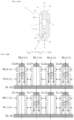
- FIGS. 8 A, 8 B and 8 C A block refresh operation of the SGT-including memory device according to a second embodiment will be described with reference to FIGS. 8 A, 8 B and 8 C .
- FIG. 8 A is a circuit diagram illustrating a memory block selected for block refreshing. Although nine memory cells CL 11 to CL 33 in three rows and three columns are illustrated, the actual memory block is larger than this matrix. To each memory cell, a corresponding one of the source lines SL 1 to SL 3 , a corresponding one of the bit lines BL 1 to BL 3 , a corresponding one of the plate lines PL 1 to PL 3 , and a corresponding one of the word lines WL 1 to WL 3 are connected. As illustrated in FIG. 8 B , to the bit lines BL 1 to BL 3 and the word lines WL 1 to WL 3 of a memory block selected for block refreshing for a “1” write state, the pulse waveforms as illustrated in FIG. 6 BC are applied.
- block refreshing is performed for each of the blocks individually, and therefore, the bit line BL, the source line SL, the plate line PL, and the word line WL can be controlled for each of the blocks independently.
- FIGS. 9 A, 9 B to 9 C are circuit block diagrams for explaining a block refresh operation for dynamic flash memory cells according to a third embodiment.
- a controller circuit 33 and a logical-physical block address conversion look-up table circuit (logical-physical address conversion table) 32 continuously manage a correspondence between data stored at a logical block address and a corresponding physical block address in the dynamic flash memory. This is because in a dynamic flash memory, in block data rewriting, a block that has already been erased is used to perform rewriting as in a flash memory, and therefore, the correspondence between the logical block address and the physical block address needs to be continuously managed.
- the controller circuit 33 and the logical-physical address conversion table 32 may be provided in the chip of the dynamic flash memory or may be provided outside the chip as illustrated in FIG. 9 A .
- An order from the logical-physical address conversion table 32 is input to a block address decoder circuit 34 , and a block to be refreshed is selected from among blocks BLK 00 to BLK 33 .
- FIG. 9 B a case where an order for refreshing storage data in, for example, the block BLK21 among 16 blocks (4 ⁇ 4 blocks), namely, the blocks BLK 00 to BLK 33 , of the dynamic flash memory is issued from the controller circuit 33 is assumed.
- the controller circuit 33 first refers to the logical-physical address conversion table 32 and specifies a block for which refreshing is necessary.
- FIG. 9 C a case where an order for refreshing storage data in, for example, three blocks BLK 12 , BLK 21 , and BLK 32 among the 16 blocks (4 ⁇ 4 blocks), namely, the blocks BLK 00 to BLK 33 , of the dynamic flash memory is issued from the controller circuit 33 is assumed.
- the controller circuit 33 first refers to the logical-physical address conversion table 32 and specifies blocks for which refreshing is necessary. As described above, a plurality of blocks can be selected and simultaneously refreshed.
- a cache memory (not illustrated) that temporarily stores storage data in a block that is to be refreshed may be necessary.
- This cache memory may be provided inside or outside the chip of the dynamic flash memory of this embodiment.
- the logical-physical address conversion table 32 or the cache memory may be constituted by a memory cell array that enables high-speed access to dynamic flash memory cells.
- a refresh operation for each block may be performed at the same time when another operation, namely, reading, writing, or erasing, is being performed for another block.
- refreshing is performed in the block at a physical address concerned, and therefore, a block rewrite operation need not be performed or a block erase operation need not be performed.
- the dynamic flash memory cells in the third embodiment are volatile memory, a block rewrite operation and a block erase operation that are functions implemented only in a flash memory, which is nonvolatile memory, are implemented, and memory cells that allow higher integration can be provided.
- a plurality of blocks can be selected upon a refresh operation and the refresh operation can be performed for the blocks simultaneously. All of the blocks in the chip of the dynamic flash memory can be simultaneously selected and the refresh operation can be performed. Accordingly, the refresh operation can be efficiently performed, and the time taken for the refresh operation can be significantly reduced.
- a plurality of blocks can be selected upon a refresh operation and the refresh operation can be performed for the blocks simultaneously.
- the memory re-write operation can be performed for a first selected block and the memory re-erase operation can be performed for a second selected block simultaneously. Accordingly, the refresh operation can be efficiently performed, and the time taken for the refresh operation can be significantly reduced.
- FIGS. 10 AA, 10 AB, and 10 BC are diagrams for explaining a step-up refresh operation for the dynamic flash memory cell according to a fourth embodiment.
- FIG. 10 AA illustrates a case where the voltage of the plate line PL is increased from the first voltage V PLL to a second voltage V PL4 in a memory re-erase operation such that the voltage is increased in increments of a first step voltage (which is an example of “first step voltage” in the claims) ⁇ V PLE with a plurality of pulse waves.
- the voltage of the word line WL is increased from the third voltage Vss to a fourth voltage V WL4 such that the voltage is increased in increments of a second step voltage (which is an example of “second step voltage” in the claims) ⁇ V WLE with a plurality of pulse waves.
- FIG. 10 AA illustrates a case where the voltage of the plate line PL is increased from the first voltage V PLL to a second voltage V PL4 in a memory re-erase operation such that the voltage is increased in increments of a first step voltage (which is an example of “first step voltage” in the claims) ⁇ V PLE with a plurality of pulse
- FIG. 10 AB illustrates a state in which the threshold voltage Vt WL “0” of the word line WL in a “0” erase state gradually rises in the step-up refresh operation.
- FIG. 10 BC illustrates a case where the first step voltage and the second step voltage are not pulse waves and the voltage of the plate line PL and the voltage of the word line WL are successively increased without being decreased to low voltages of the first voltage and the third voltage respectively.
- the step-up refresh operation as described above the voltages can be made closer to the desired voltages in the “0” erase state without a large electric field being applied to individual dynamic flash memory cells for which the refresh operation is performed.
- the variation can be resolved by performing the step-up refresh operation without application of an intense electric field. As a result, a highly reliable refresh operation can be performed.
- Si column is formed in the present invention
- a semiconductor column made of a semiconductor material other than Si may be formed. The same applies to other embodiments according to the present invention.
- the logical-physical address conversion table illustrated in FIGS. 9 A, 9 B and 9 C in the third embodiment may be constituted by a dynamic flash memory that enables high-speed access to memory elements. The same applies to other embodiments according to the present invention.
- Each of the blocks BLK 00 to BLK 33 illustrated in FIGS. 9 A, 9 B and 9 C in the third embodiment may be provided with a timer circuit (not illustrated), and the blocks may be refreshed in accordance with instructions of the respective timer circuits. The same applies to other embodiments according to the present invention.
- a vertical NAND-type flash memory circuit memory cells that are stacked in a plurality of tiers in the vertical direction and each of which is constituted by a semiconductor column, which functions as the channel, and a tunnel oxide layer, a charge storage layer, an interlayer insulating layer, and a control conductor layer that surround the semiconductor column are formed.
- a source line impurity region corresponding to the source and a bit line impurity region corresponding to the drain are disposed respectively.
- the vertical NAND-type flash memory circuit is one type of SGT circuit. Therefore, the present invention is also applicable to a circuit in which a NAND-type flash memory circuit coexists.
- electron-positive hole pairs may be generated by an impact ionization phenomenon using a gate-induced drain leakage (GIDL) current described in E. Yoshida, and T. Tanaka: “A Capacitorless 1T-DRAM Technology Using Gate-Induced Drain-Leakage (GIDL) Current for Low-Power and High-Speed Embedded Memory”, IEEE Transactions on Electron Devices, Vol. 53, No. 4, pp. 692-69, Apr. 2006, and the floating body FB may be filled with the generated group of positive holes. The same applies to other embodiments according to the present invention.
- GIDL gate-induced drain leakage
- the operations of the dynamic flash memory can be performed.
- the Si column 2 that is of N-type the majority carriers are electrons. Therefore, a group of electrons generated by impact ionization are stored in the semiconductor body 7 , and a “1” state is set.
Landscapes
- Engineering & Computer Science (AREA)
- Microelectronics & Electronic Packaging (AREA)
- Computer Hardware Design (AREA)
- Dram (AREA)
- Semiconductor Memories (AREA)
- Read Only Memory (AREA)
Abstract
Description
C FB =C WL +C BL +C SL (14)
The capacitive coupling ratio βWL between the gate to which the word line is connected and the floating body is expressed as follows.
βWL =C WL/(C WL+CBL +C SL) (15)
Therefore, a change in the word line voltage VWL at the time of reading or writing affects the voltage of the floating
Here, for βWL in expression (15), the contribution ratio of CWL is large and, for example, CWL:CBL:CSL=8:1:1 holds. This results in βWL=0.8. When the word line changes, for example, from 5 V at the time of writing to 0 V after the end of writing, the floating
-
- each of the memory cells included in the block including:
- a semiconductor body that stands on the substrate in a vertical direction relative to the substrate or that extends along the substrate in a horizontal direction relative to the substrate;
- a first impurity region and a second impurity region that are disposed at respective ends of the semiconductor body;
- a gate insulator layer that is in contact with a side surface of the semiconductor body between the first impurity region and the second impurity region;
- a first gate conductor layer that partially or entirely covers the gate insulator layer; and
- a second gate conductor layer that is adjacent to the first gate conductor layer and that is in contact with a side surface of the gate insulator layer, in which
- in each of the memory cells,
- voltages applied to the first gate conductor layer, the second gate conductor layer, the first impurity region, and the second impurity region are controlled to retain a group of positive holes, generated by an impact ionization phenomenon or a gate-induced drain leakage current, inside the semiconductor body,
- a memory write operation is performed in which a voltage of the semiconductor body is made equal to a first data retention voltage that is higher than the voltage of one of the first impurity region or the second impurity region or the voltages of both of the first impurity region and the second impurity region by a built-in voltage,
- a memory erase operation is performed in which the voltage of the semiconductor body is controlled so as to be higher than the first data retention voltage with first capacitive coupling between the first gate conductor layer and the semiconductor body and second capacitive coupling between the second gate conductor layer and the semiconductor body, and a group of remaining positive holes among the group of positive holes are discharged from inside the semiconductor body through one or both of the first impurity region and the second impurity region until the voltage of the semiconductor body becomes equal to a voltage higher than the voltage of one of the first impurity region or the second impurity region or the voltages of both of the first impurity region and the second impurity region by the built-in voltage, and
- in which the voltage of the semiconductor body is made equal to a second data retention voltage lower than the first data retention voltage with the first capacitive coupling and the second capacitive coupling,
- the voltage of the semiconductor body in each of the plurality of memory cells in the block is equal to the first data retention voltage or the second data retention voltage at a first time,
- at a second time after a lapse of time since the first time, a memory re-write operation is performed for the semiconductor body, in the block, that is at a voltage equal to the first data retention voltage at the first time to return the voltage of the semiconductor body to a voltage close to the first data retention voltage, and
- at a third time after a lapse of time since the first time, a memory re-erase operation is performed for the semiconductor body, in the block, that is at a voltage equal to the second data retention voltage at the first time to return the voltage of the semiconductor body to a voltage close to the second data retention voltage (first invention).
-
- the memory re-erase operation is performed over a first period, a second period, and a third period,
- in the first period, the voltage of the semiconductor body is controlled so as to be higher than the voltage at the first time with the first capacitive coupling and the second capacitive coupling,
- in the second period, the group of remaining positive holes among the group of positive holes are discharged from inside the semiconductor body through one or both of the first impurity region and the second impurity region until the voltage of the semiconductor body becomes equal to a voltage higher than the voltage of one of the first impurity region or the second impurity region or the voltages of both of the first impurity region and the second impurity region by the built-in voltage, and
- in the third period, the voltage of the semiconductor body is made equal to a voltage close to the second data retention voltage lower than the first data retention voltage with the first capacitive coupling and the second capacitive coupling (second invention).
-
- the first impurity region is connected to a source line, the second impurity region is connected to a bit line, one of the first gate conductor layer or the second gate conductor layer is connected to a word line, and the other of the first gate conductor layer or the second gate conductor layer is connected to a first driving control line,
- the source line is connected to the semiconductor bodies in each of the blocks, and
- voltages are applied to the source line, the bit line, the first driving control line, and the word line to perform one of the memory re-write operation or the memory re-erase operation for all of the semiconductor bodies in a block selected from among the group of blocks or simultaneously perform both of the memory re-write operation and the memory re-erase operation for all of the semiconductor bodies in respective blocks selected from among the group of blocks (seventh invention).
C FB =C WL +C PL +C BL +C SL (1)
Therefore, the coupling ratio βWL between the word line WL and the
βWL =C WL/(C WL +C PL +C BL +C SL) (2)
βPL =C PL/(C WL +C PL +C BL +C SL) (3)
βBL =C BL/(C WL +C PL +C BL +C SL) (4)
βSL =C SL/(C WL +C PL +C BL +C SL) (5)
Here, CPL>CWL holds, and therefore, this results in βPL>βWL.
The coupling ratio βWL between the word line WL and the
V FB“1”=Vb−β WL ×Vt WL“1”−βWL ×V BLH (7)
Here, the coupling ratio βBL between the bit line BL and the
Here, the sum of βWL and βPL is greater than or equal to 0.8, ΔVFB is large, and a sufficient margin is provided. As a result, as illustrated in
βBL =C VL/(C WL +C L +C BL +C SL) (4)
V FB2 =V FB1βBL ×V BLR (10)
The description of the block refresh operation for the dynamic flash memory cells in the “1” write state according to the first embodiment of the present invention will be continued with reference to
Vb1=Vb−β WL ×Vt WL“1” (11)
Here, the threshold voltage VtWL“1” in the “1” write state is low, and therefore, βWL×VtWL“1” is small. Subsequently, at time T4, the bit line BL drops from VSLR to Vss, and the block refresh operation for the “1” write state ends. The voltage VFB“1” of the
V FB“0”=Vb−β WL ×V WLRE−βPL×(V PLR −V PLL) (13)
Therefore, as illustrated in
Claims (9)
Applications Claiming Priority (1)
| Application Number | Priority Date | Filing Date | Title |
|---|---|---|---|
| PCT/JP2021/003248 WO2022162870A1 (en) | 2021-01-29 | 2021-01-29 | Memory device using semiconductor elements |
Related Parent Applications (1)
| Application Number | Title | Priority Date | Filing Date |
|---|---|---|---|
| PCT/JP2021/003248 Continuation-In-Part WO2022162870A1 (en) | 2021-01-29 | 2021-01-29 | Memory device using semiconductor elements |
Publications (2)
| Publication Number | Publication Date |
|---|---|
| US20230377658A1 US20230377658A1 (en) | 2023-11-23 |
| US12315570B2 true US12315570B2 (en) | 2025-05-27 |
Family
ID=81291710
Family Applications (1)
| Application Number | Title | Priority Date | Filing Date |
|---|---|---|---|
| US18/226,656 Active 2041-06-03 US12315570B2 (en) | 2021-01-29 | 2023-07-26 | Semiconductor element memory device |
Country Status (4)
| Country | Link |
|---|---|
| US (1) | US12315570B2 (en) |
| JP (1) | JP7057037B1 (en) |
| TW (1) | TWI793973B (en) |
| WO (1) | WO2022162870A1 (en) |
Families Citing this family (7)
| Publication number | Priority date | Publication date | Assignee | Title |
|---|---|---|---|---|
| WO2022168220A1 (en) * | 2021-02-04 | 2022-08-11 | ユニサンティス エレクトロニクス シンガポール プライベート リミテッド | Memory device using semiconductor element |
| WO2023238370A1 (en) | 2022-06-10 | 2023-12-14 | ユニサンティス エレクトロニクス シンガポール プライベート リミテッド | Semiconductor memory device |
| JPWO2023242956A1 (en) * | 2022-06-14 | 2023-12-21 | ||
| WO2024018556A1 (en) | 2022-07-20 | 2024-01-25 | ユニサンティス エレクトロニクス シンガポール プライベート リミテッド | Memory device using semiconductor element |
| WO2024053015A1 (en) * | 2022-09-07 | 2024-03-14 | ユニサンティス エレクトロニクス シンガポール プライベート リミテッド | Memory device using semiconductor element |
| US20240179886A1 (en) * | 2022-11-28 | 2024-05-30 | Unisantis Electronics Singapore Pte. Ltd. | Memory-element-including semiconductor device |
| CN118265288A (en) * | 2022-12-26 | 2024-06-28 | 长江存储科技有限责任公司 | Memory device and method for forming a memory device |
Citations (9)
| Publication number | Priority date | Publication date | Assignee | Title |
|---|---|---|---|---|
| JPH02188966A (en) | 1989-01-17 | 1990-07-25 | Toshiba Corp | Mos semiconductor device |
| JPH03171768A (en) | 1989-11-30 | 1991-07-25 | Toshiba Corp | Semiconductor storage device |
| US20030111681A1 (en) | 2001-12-14 | 2003-06-19 | Kabushiki Kaisha Toshiba | Semiconductor memory device and its manufacturing method |
| US20060049444A1 (en) | 2004-09-09 | 2006-03-09 | Kabushiki Kaisha Toshiba | Semiconductor device and method of fabricating the same |
| JP3957774B2 (en) | 1995-06-23 | 2007-08-15 | 株式会社東芝 | Semiconductor device |
| US20080137394A1 (en) | 2006-12-12 | 2008-06-12 | Renesas Technology Corp. | Semiconductor memory device |
| US20080212366A1 (en) | 2007-03-01 | 2008-09-04 | Kabushiki Kaisha Toshiba | Semiconductor memory device |
| US8154086B2 (en) * | 2008-01-29 | 2012-04-10 | Unisantis Electronics Singapore Pte Ltd. | Semiconductor surround gate SRAM storage device |
| US12205629B2 (en) * | 2021-10-19 | 2025-01-21 | Unisantis Electronics Singapore Pte. Ltd. | Semiconductor-element-including memory device |
Family Cites Families (2)
| Publication number | Priority date | Publication date | Assignee | Title |
|---|---|---|---|---|
| US10651189B2 (en) * | 2014-03-04 | 2020-05-12 | Unisantis Electronics Singapore Pte. Ltd. | Method for producing pillar-shaped semiconductor memory device |
| JP7231282B2 (en) * | 2019-06-05 | 2023-03-01 | ユニサンティス エレクトロニクス シンガポール プライベート リミテッド | Method for manufacturing columnar semiconductor device |
-
2021
- 2021-01-29 WO PCT/JP2021/003248 patent/WO2022162870A1/en not_active Ceased
- 2021-01-29 JP JP2021525273A patent/JP7057037B1/en active Active
-
2022
- 2022-01-13 TW TW111101485A patent/TWI793973B/en active
-
2023
- 2023-07-26 US US18/226,656 patent/US12315570B2/en active Active
Patent Citations (11)
| Publication number | Priority date | Publication date | Assignee | Title |
|---|---|---|---|---|
| JPH02188966A (en) | 1989-01-17 | 1990-07-25 | Toshiba Corp | Mos semiconductor device |
| JPH03171768A (en) | 1989-11-30 | 1991-07-25 | Toshiba Corp | Semiconductor storage device |
| JP3957774B2 (en) | 1995-06-23 | 2007-08-15 | 株式会社東芝 | Semiconductor device |
| US20030111681A1 (en) | 2001-12-14 | 2003-06-19 | Kabushiki Kaisha Toshiba | Semiconductor memory device and its manufacturing method |
| US20060049444A1 (en) | 2004-09-09 | 2006-03-09 | Kabushiki Kaisha Toshiba | Semiconductor device and method of fabricating the same |
| JP2006080280A (en) | 2004-09-09 | 2006-03-23 | Toshiba Corp | Semiconductor device and manufacturing method thereof |
| US20080137394A1 (en) | 2006-12-12 | 2008-06-12 | Renesas Technology Corp. | Semiconductor memory device |
| US20080212366A1 (en) | 2007-03-01 | 2008-09-04 | Kabushiki Kaisha Toshiba | Semiconductor memory device |
| JP2008218556A (en) | 2007-03-01 | 2008-09-18 | Toshiba Corp | Semiconductor memory device |
| US8154086B2 (en) * | 2008-01-29 | 2012-04-10 | Unisantis Electronics Singapore Pte Ltd. | Semiconductor surround gate SRAM storage device |
| US12205629B2 (en) * | 2021-10-19 | 2025-01-21 | Unisantis Electronics Singapore Pte. Ltd. | Semiconductor-element-including memory device |
Non-Patent Citations (19)
| Title |
|---|
| E. Yoshida and T. Tanaka: "A Design of a Capacitorless 1T-DRAM Cell Using Gate-induced Drain Leakage (GIDL) Current for Low-power and High-speed Embedded Memory," IEEE IEDM, pp. 913-916, Dec. 2003. |
| E. Yoshida, and T. Tanaka: "A Capacitorless 1T-DRAM Technology Using Gate-Induced Drain-Leakage (GIDL) Current for Low-Power and High-Speed Embedded Memory," IEEE Transactions on Electron Devices, vol. 53, No. 4, pp. 692-697, Apr. 2006. |
| English translation of International Search of Search Report (PCT/ISA/210) of PCT/JP2021/003248, 2 pgs. |
| F. Morishita, H. Noda, I. Hayashi, T. Gyohten, M. Okamoto, T. Ipposhi, S. Maegawa, K. Dosaka, and K. Arimoto: "A Capacitorless Twin-Transistor Random Access Memory (TTRAM) on SOI," IEICE Trans. Electron., vol. E90-c., No. 4 pp. 765-771 (2007) a brief description attached. |
| F. Morishita, H. Noda, I. Hayashi, T. Gyohten, M. Oksmoto, T. Ipposhi, S. Maegawa, K. Dosaka, and K. Arimoto: "A Capacitorless Twin-Transistor Random Access Memory (TTRAM) on SOI," IEICE Trans. Electron., vol. E90-c., No. 4 pp. 765-771 (2007). |
| H. Chung, H. Kim, H. Kim, K. Kim, S. Kim, K. Dong, J. Kim, Y. C. Oh, Y. Hwang, H. Hong, G. Jin, and C. Chung: "Novel 4F2 DRAM Cell with Vertical Pillar Transistor (VPT)," 2011 Proceeding of the European Solid-State Device Research Conference, (2011). |
| H. Jiang, N. Xu, B. Chen, L. Zeng1, Y. He, G. Du, X. Liu and X. Zhang: "Experimental investigation of self heating effect (SHE) in multiple-fin SOI F inFETs," Semicond. Sci. Technol. 29 (2014) 115021 (7 pp). |
| H. S. Philip Wong, S. Raoux, S. Kim, Jiale Liang, J. R. Reifenberg, B. Rajendran, M. Asheghi and K. E. Goodson: "Phase Change Memory," Proceeding of IEEE, vol. 98, No. 12, December, pp. 2201-2227 (2010). |
| Hiroshi Takato, Kazumasa Sunouchi, Naoko Okabe, Akihiro Nitayama, Katsuhiko Hieda, Fumio Horiguchi, and Fujio Masuoka: IEEE Transaction on Electron Devices, vol. 38, No. 3, pp. 573-578 (1991). |
| International Search Report (PCT/ISA/210) (Japanese) from PCT/JP2021/003248 dated March 30, 2021, 3 pgs. |
| J. Wan, L. Rojer, A. Zaslavsky, and S. Critoloveanu: "A Compact Capacitor-Less High-Speed DRAM Using Field Effect-Controlled Charge Regeneration," Electron Device Letters, vol. 35, No. 2, pp. 179-181 (2012). |
| J. Y. Song, W. Y. Choi, J. H. Park, J. D. Lee, and B-G. Park: "Design Optimization of Gate-All-Around (GAA) MOSFETs," IEEE Trans. Electron Devices, vol. 5, No. 3, pp. 186-191, May 2006. |
| M. G. Ertosum, K. Lim, C. Park, J. Oh, P. Kirsch, and K. C. Saraswat: "Novel Capacitorless Single-Transistor Charge-Trap DRAM (1T CT DRAM) Utilizing Electron," IEEE Electron Device Letter, vol. 31, No. 5, pp. 405-407 (2010). |
| N. Loubet, et al.: "Stacked Nanosheet Gate-All-Around Transistor to Enable Scaling Beyond FinFET," 2017 IEEE Symposium on VLSI Technology Digest of Technical Papers, T17-5, T230-T231, Jun. 2017. |
| T. Ohsawa, K. Fujita, T. Higashi, Y. Iwata, T. Kajiyama, Y. Asao, and K. Sunouchi: "Memory design using a one-transistor gain cell on SOI," IEEE JSSC, vol. 37, No. 11, pp. 1510-1522 (2002). |
| T. Shino, N. Kusunoki, T. Higashi, T. Ohsawa, K. Fujita, K. Hatsuda, N. Ikumi, F. Matsuoka, Y. Kajitani, R. Fukuda, Y. Watanabe, Y. Minami, A. Sakamoto, J. Nishimura, H. Nakajima, M. Morikado, K. Inoh, T. Hamamoto, A. Nitayama: "Floating Body RAM Technology and its Scalability to 32nm Node and Beyond," IEEE IEDM (2006). |
| T. Tsunoda, K. Kinoshita, H. Noshiro, Y. Yamazaki, T. Iizuka, Y. Ito, A. Takahashi, A. Okano, Y. Sato, T. Fukano, M. Aoki, and Y. Sugiyama: "Low Power and high Speed Switching of Ti-doped NiO ReRAM under the Unipolar Voltage Source of less than 3V," IEDM (2007). |
| W. Kang, L. Zhang, J. Klein, Y. Zhang, D. Ravelosona, and W. Zhao: "Reconfigurable Codesign of STT-MRAM Under Process Variations in Deeply Scaled Technology," IEEE Transaction on Electron Devices, pp. 1-9 (2015). |
| Written Opinion (PCT/ISA/237) (Japanese) of PCT/JP2021/003248 dated Mar. 3, 2021, 3pgs. |
Also Published As
| Publication number | Publication date |
|---|---|
| TWI793973B (en) | 2023-02-21 |
| JPWO2022162870A1 (en) | 2022-08-04 |
| JP7057037B1 (en) | 2022-04-19 |
| US20230377658A1 (en) | 2023-11-23 |
| WO2022162870A1 (en) | 2022-08-04 |
| TW202243217A (en) | 2022-11-01 |
Similar Documents
| Publication | Publication Date | Title |
|---|---|---|
| US12315570B2 (en) | Semiconductor element memory device | |
| US12131773B2 (en) | Memory device | |
| US12100443B2 (en) | Semiconductor-element-including memory device | |
| US11763877B2 (en) | Semiconductor-element-including memory device | |
| US11823727B2 (en) | Semiconductor element memory device | |
| US12096611B2 (en) | Semiconductor element memory device | |
| US12185522B2 (en) | Memory apparatus using semiconductor devices | |
| US12277962B2 (en) | Memory device using semiconductor element | |
| US11682443B2 (en) | Semiconductor element memory device | |
| US12245417B2 (en) | Semiconductor-element-including memory device | |
| US11823726B2 (en) | Semiconductor element memory device | |
| US12317479B2 (en) | Memory apparatus using semiconductor devices | |
| US12205629B2 (en) | Semiconductor-element-including memory device | |
| US12166107B2 (en) | Semiconductor-element-including memory device | |
| US12376284B2 (en) | Memory device using dynamic flash memory cells | |
| US12402296B2 (en) | Semiconductor element memory device | |
| US12518820B2 (en) | Memory device having a matrix of SGT memory cells | |
| US12367922B2 (en) | Semiconductor element memory device | |
| US12367923B2 (en) | Semiconductor element memory device | |
| US12249366B2 (en) | Semiconductor-element-including memory device | |
| US20230397397A1 (en) | Semiconductor element memory device | |
| US12315563B2 (en) | Memory apparatus using semiconductor devices | |
| US12279412B2 (en) | Semiconductor element memory device |
Legal Events
| Date | Code | Title | Description |
|---|---|---|---|
| FEPP | Fee payment procedure |
Free format text: ENTITY STATUS SET TO UNDISCOUNTED (ORIGINAL EVENT CODE: BIG.); ENTITY STATUS OF PATENT OWNER: SMALL ENTITY |
|
| AS | Assignment |
Owner name: UNISANTIS ELECTRONICS SINGAPORE PTE. LTD., SINGAPORE Free format text: ASSIGNMENT OF ASSIGNORS INTEREST;ASSIGNORS:SAKUI, KOJI;HARADA, NOZOMU;REEL/FRAME:064407/0739 Effective date: 20230512 |
|
| FEPP | Fee payment procedure |
Free format text: ENTITY STATUS SET TO SMALL (ORIGINAL EVENT CODE: SMAL); ENTITY STATUS OF PATENT OWNER: SMALL ENTITY |
|
| STPP | Information on status: patent application and granting procedure in general |
Free format text: DOCKETED NEW CASE - READY FOR EXAMINATION |
|
| STPP | Information on status: patent application and granting procedure in general |
Free format text: NON FINAL ACTION MAILED |
|
| STPP | Information on status: patent application and granting procedure in general |
Free format text: RESPONSE TO NON-FINAL OFFICE ACTION ENTERED AND FORWARDED TO EXAMINER |
|
| STPP | Information on status: patent application and granting procedure in general |
Free format text: NOTICE OF ALLOWANCE MAILED -- APPLICATION RECEIVED IN OFFICE OF PUBLICATIONS |
|
| STCF | Information on status: patent grant |
Free format text: PATENTED CASE |