US12307990B2 - Microfluidic pixel driving circuit, microfluidic substrate, and microfluidic chip - Google Patents
Microfluidic pixel driving circuit, microfluidic substrate, and microfluidic chip Download PDFInfo
- Publication number
- US12307990B2 US12307990B2 US18/387,304 US202318387304A US12307990B2 US 12307990 B2 US12307990 B2 US 12307990B2 US 202318387304 A US202318387304 A US 202318387304A US 12307990 B2 US12307990 B2 US 12307990B2
- Authority
- US
- United States
- Prior art keywords
- scan
- capacitor
- data
- line
- electrically connected
- Prior art date
- Legal status (The legal status is an assumption and is not a legal conclusion. Google has not performed a legal analysis and makes no representation as to the accuracy of the status listed.)
- Active
Links
Images


Classifications
-
- G—PHYSICS
- G09—EDUCATION; CRYPTOGRAPHY; DISPLAY; ADVERTISING; SEALS
- G09G—ARRANGEMENTS OR CIRCUITS FOR CONTROL OF INDICATING DEVICES USING STATIC MEANS TO PRESENT VARIABLE INFORMATION
- G09G3/00—Control arrangements or circuits, of interest only in connection with visual indicators other than cathode-ray tubes
- G09G3/20—Control arrangements or circuits, of interest only in connection with visual indicators other than cathode-ray tubes for presentation of an assembly of a number of characters, e.g. a page, by composing the assembly by combination of individual elements arranged in a matrix no fixed position being assigned to or needed to be assigned to the individual characters or partial characters
- G09G3/34—Control arrangements or circuits, of interest only in connection with visual indicators other than cathode-ray tubes for presentation of an assembly of a number of characters, e.g. a page, by composing the assembly by combination of individual elements arranged in a matrix no fixed position being assigned to or needed to be assigned to the individual characters or partial characters by control of light from an independent source
- G09G3/3433—Control arrangements or circuits, of interest only in connection with visual indicators other than cathode-ray tubes for presentation of an assembly of a number of characters, e.g. a page, by composing the assembly by combination of individual elements arranged in a matrix no fixed position being assigned to or needed to be assigned to the individual characters or partial characters by control of light from an independent source using light modulating elements actuated by an electric field and being other than liquid crystal devices and electrochromic devices
- G09G3/348—Control arrangements or circuits, of interest only in connection with visual indicators other than cathode-ray tubes for presentation of an assembly of a number of characters, e.g. a page, by composing the assembly by combination of individual elements arranged in a matrix no fixed position being assigned to or needed to be assigned to the individual characters or partial characters by control of light from an independent source using light modulating elements actuated by an electric field and being other than liquid crystal devices and electrochromic devices based on the deformation of a fluid drop, e.g. electrowetting
-
- G—PHYSICS
- G09—EDUCATION; CRYPTOGRAPHY; DISPLAY; ADVERTISING; SEALS
- G09G—ARRANGEMENTS OR CIRCUITS FOR CONTROL OF INDICATING DEVICES USING STATIC MEANS TO PRESENT VARIABLE INFORMATION
- G09G2310/00—Command of the display device
- G09G2310/02—Addressing, scanning or driving the display screen or processing steps related thereto
- G09G2310/0264—Details of driving circuits
- G09G2310/0267—Details of drivers for scan electrodes, other than drivers for liquid crystal, plasma or OLED displays
-
- G—PHYSICS
- G09—EDUCATION; CRYPTOGRAPHY; DISPLAY; ADVERTISING; SEALS
- G09G—ARRANGEMENTS OR CIRCUITS FOR CONTROL OF INDICATING DEVICES USING STATIC MEANS TO PRESENT VARIABLE INFORMATION
- G09G2310/00—Command of the display device
- G09G2310/02—Addressing, scanning or driving the display screen or processing steps related thereto
- G09G2310/0264—Details of driving circuits
- G09G2310/0275—Details of drivers for data electrodes, other than drivers for liquid crystal, plasma or OLED displays, not related to handling digital grey scale data or to communication of data to the pixels by means of a current
Definitions
- the present disclosure relates to the field of display technology and, in particular, to a microfluidic pixel driving circuit, a microfluidic substrate, and a microfluidic chip.
- a microfluidic chip has strong integrity and has a fast analysis speed, a low loss, low material consumption, and small pollution when used for processing samples. Therefore, the microfluidic chip is widely applied in many fields such as biomedical research, drug synthesis and screening, environmental monitoring and protection, health quarantine, judicial identification, and the detection of biological reagents.
- An existing microfluidic chip is mainly used for driving a droplet to flow.
- a microfluidic pixel driving circuit working in the microfluidic chip requires a relatively high drive voltage, which poses a challenge to a driver chip for the microfluidic chip.
- the present disclosure provides a microfluidic pixel driving circuit, a microfluidic substrate, and a microfluidic chip.
- a microfluidic pixel driving circuit includes n boost modules, where each of the n boost modules includes a capacitor and a write unit, a capacitor in a first boost module of the n boost modules is denoted as a first capacitor, a write unit in the first one of the n boost modules is denoted as a first write unit, a capacitor in a second boost module of the n boost modules is denoted as a second capacitor, a write unit in the second one of the n boost modules is denoted as a second write unit, and n is a positive integer greater than or equal to 2.
- a first terminal of the first capacitor is electrically connected to a fixed potential line, a second terminal of the first capacitor is electrically connected to a pixel electrode, and the first capacitor is used for storing a voltage of the pixel electrode.
- the first write unit is configured to write a first data signal to the pixel electrode according to an enable level of a first scan signal.
- a first terminal of the second capacitor is electrically connected to the pixel electrode.
- the second write unit is configured to write a second data signal to a second terminal of the second capacitor according to an enable level of a second scan signal.
- a microfluidic substrate includes a substrate and a pixel unit on a side of the substrate.
- the pixel unit includes a microfluidic pixel driving circuit and a pixel electrode, where the microfluidic pixel driving circuit is electrically connected to the pixel electrode, and includes n boost modules, where each of the n boost modules includes a capacitor and a write unit, a capacitor in a first boost module of the n boost modules is denoted as a first capacitor, a write unit in the first one of the n boost modules is denoted as a first write unit, a capacitor in a second boost module of the n boost modules is denoted as a second capacitor, a write unit in the second one of the n boost modules is denoted as a second write unit, and n is a positive integer greater than or equal to 2.
- a first terminal of the first capacitor is electrically connected to a fixed potential line, a second terminal of the first capacitor is electrically connected to a pixel electrode, and the first capacitor is used for storing a voltage of the pixel electrode.
- the first write unit is configured to write a first data signal to the pixel electrode according to an enable level of a first scan signal.
- a first terminal of the second capacitor is electrically connected to the pixel electrode.
- the second write unit is configured to write a second data signal to a second terminal of the second capacitor according to an enable level of a second scan signal.
- a microfluidic chip includes a microfluidic substrate, an opposing substrate, and a channel layer, where the channel layer is disposed between the opposing substrate and the microfluidic substrate and used for accommodating a droplet.
- the microfluidic substrate includes a substrate and a pixel unit on a side of the substrate.
- the pixel unit includes a microfluidic pixel driving circuit and a pixel electrode, where the microfluidic pixel driving circuit is electrically connected to the pixel electrode, and includes n boost modules, where each of the n boost modules includes a capacitor and a write unit, a capacitor in a first boost module of the n boost modules is denoted as a first capacitor, a write unit in the first one of the n boost modules is denoted as a first write unit, a capacitor in a second boost module of the n boost modules is denoted as a second capacitor, a write unit in the second one of the n boost modules is denoted as a second write unit, and n is a positive integer greater than or equal to 2.
- a first terminal of the first capacitor is electrically connected to a fixed potential line, a second terminal of the first capacitor is electrically connected to a pixel electrode, and the first capacitor is used for storing a voltage of the pixel electrode.
- the first write unit is configured to write a first data signal to the pixel electrode according to an enable level of a first scan signal.
- a first terminal of the second capacitor is electrically connected to the pixel electrode.
- the second write unit is configured to write a second data signal to a second terminal of the second capacitor according to an enable level of a second scan signal.
- FIG. 1 is a circuit diagram of a microfluidic pixel driving circuit according to an embodiment of the present disclosure.
- FIG. 2 is another circuit diagram of a microfluidic pixel driving circuit according to an embodiment of the present disclosure.
- FIG. 3 is a drive timing diagram of a microfluidic pixel driving circuit according to an embodiment of the present disclosure.
- FIG. 4 is another drive timing diagram of a microfluidic pixel driving circuit according to an embodiment of the present disclosure.
- FIG. 5 is another drive timing diagram of a microfluidic pixel driving circuit according to an embodiment of the present disclosure.
- FIG. 6 is a top view illustrating the structure of a microfluidic substrate according to an embodiment of the present disclosure.
- FIG. 7 is a top view illustrating the structure of a pixel unit according to an embodiment of the present disclosure.
- FIG. 8 is a sectional view of the pixel unit of FIG. 7 taken along a direction AA′.
- FIG. 9 is another top view illustrating the structure of a pixel unit according to an embodiment of the present disclosure.
- FIG. 10 is a sectional view of the pixel unit of FIG. 9 taken along a direction BB′.
- FIG. 11 is another top view illustrating the structure of a pixel unit according to an embodiment of the present disclosure.
- FIG. 12 is a sectional view of the pixel unit of FIG. 11 taken along a direction CC′.
- FIG. 13 is another top view illustrating the structure of a pixel unit according to an embodiment of the present disclosure.
- FIG. 14 is a sectional view of the pixel unit of FIG. 13 taken along a direction DD′.
- FIG. 15 is another top view illustrating the structure of a pixel unit according to an embodiment of the present disclosure.
- FIG. 16 is a sectional view of the pixel unit of FIG. 15 taken along a direction EE′.
- FIG. 17 is another top view illustrating the structure of a pixel unit according to an embodiment of the present disclosure.
- FIG. 18 is a sectional view of the pixel unit of FIG. 17 taken along a direction FF′.
- FIG. 19 is another top view illustrating the structure of a pixel unit according to an embodiment of the present disclosure.
- FIG. 20 is a sectional view of the pixel unit of FIG. 19 taken along a direction GG′.
- FIG. 21 is another top view illustrating the structure of a pixel unit according to an embodiment of the present disclosure.
- FIG. 22 is a sectional view of the pixel unit of FIG. 21 taken along a direction HH′.
- FIG. 23 is another top view illustrating the structure of a pixel unit according to an embodiment of the present disclosure.
- FIG. 24 is a sectional view of the pixel unit of FIG. 23 taken along a direction II′.
- FIG. 25 is another top view illustrating the structure of a pixel unit according to an embodiment of the present disclosure.
- FIG. 26 is another top view illustrating the structure of a microfluidic substrate according to an embodiment of the present disclosure.
- FIG. 27 is a drive timing diagram of a microfluidic substrate according to an embodiment of the present disclosure.
- FIG. 28 is another drive timing diagram of a microfluidic substrate according to an embodiment of the present disclosure.
- FIG. 29 is a sectional view illustrating the structure of a microfluidic chip according to an embodiment of the present disclosure.
- FIG. 1 is a circuit diagram of a microfluidic pixel driving circuit according to an embodiment of the present disclosure.
- a microfluidic pixel driving circuit 110 includes n boost modules 111 .
- Each boost module 111 includes a capacitor C and a write unit 10 .
- a capacitor C in a first boost module 111 of the n boost modules 111 is denoted as a first capacitor C 1
- a write unit 10 in the first boost module 111 is denoted as a first write unit 11 .
- a capacitor C in a second boost module 111 of the n boost modules 111 is denoted as a second capacitor C 2
- a write unit 10 in the second boost module 111 is denoted as a second write unit 12
- n is a positive integer greater than or equal to 2.
- a first terminal of the first capacitor C 1 is electrically connected to a fixed potential line COM, and a second terminal of the first capacitor C 1 is electrically connected to a pixel electrode (not shown in FIG. 1 ).
- the first capacitor C 1 is used for storing a voltage of the pixel electrode, that is, the first capacitor C 1 is used for storing a voltage of a first node Vp.
- the first write unit 11 is configured to write a first data signal S 1 to the pixel electrode according to an enable level of a first scan signal G 1 .
- the enable level refers to a level for controlling the first write unit 11 to be turned on.
- a disable level is reverse to the enable level. Under the control of a disable level of the first scan signal G 1 , the first write unit 11 is turned off and the first write unit 11 cannot write the first data signal S 1 to the pixel electrode.
- a first terminal of the second capacitor C 2 is electrically connected to the pixel electrode.
- the first terminal of the second capacitor C 2 is connected to the first node Vp.
- a second terminal of the second capacitor C 2 is connected to a second node V 2 .
- the second write unit 12 is configured to write a second data signal S 2 to the second terminal of the second capacitor C 2 according to an enable level of a second scan signal G 2 . Under the control of a disable level of the second scan signal G 2 , the second write unit 12 is turned off and the second write unit 12 cannot write the second data signal S 2 to the pixel electrode.
- the second data signal S 2 is different from the first data signal S 1 .
- the embodiments of the present disclosure provide a microfluidic pixel driving circuit, where the microfluidic pixel driving circuit includes n boost modules 111 , each boost module 111 includes a capacitor C and a write unit 10 , and when the write unit 10 is turned on, a voltage written to the capacitor C can be fed to the pixel electrode so that the voltage written to the pixel electrode can be boosted.
- the multiple boost modules 111 can perform multi-stage boosting on the voltage written to the pixel electrode so that the voltage value of the pixel electrode is increased and the pixel electrode can drive, at a relatively high voltage, a droplet to flow without increasing the requirement on a driver chip.
- FIG. 2 is another circuit diagram of a microfluidic pixel driving circuit according to an embodiment of the present disclosure.
- the first write unit 11 includes a first transistor M 1 , a gate of the first transistor M 1 receives the first scan signal G 1 , a first electrode of the first transistor M 1 is electrically connected to the pixel electrode, and a second electrode of the first transistor M 1 receives the first data signal S 1 .
- the enable level of the first scan signal G 1 controls the first transistor M 1 to be turned on
- the first data signal S 1 is transmitted to the first node Vp via the first transistor M 1 and written to the pixel electrode, and the voltage of the pixel electrode is increased.
- the second write unit 12 includes a second transistor M 2 , a gate of the second transistor M 2 receives the second scan signal G 2 , a first electrode of the second transistor M 2 is electrically connected to the second terminal of the second capacitor C 2 , and a second electrode of the second transistor M 2 receives the second data signal S 2 .
- the enable level of the second scan signal G 2 controls the second transistor M 2 to be turned on
- the second data signal S 2 is transmitted to the second node V 2 via the second transistor M 2
- a voltage of the second node V 2 is increased and fed to the first node Vp through the second capacitor C 2
- a voltage of the first node Vp is increased again so that the voltage of the pixel electrode is increased again.
- the microfluidic pixel driving circuit further includes a third-stage boost module 111 , where a capacitor C in the third-stage boost module 111 is denoted as a third capacitor C 3 and a write unit 10 in the third-stage boost module 111 is denoted as a third write unit 13 .
- a first terminal of the third capacitor C 3 is electrically connected to the second terminal of the second capacitor C 2 .
- the first terminal of the third capacitor C 3 is connected to the second node V 2 .
- a second terminal of the third capacitor C 3 is connected to a third node V 3 .
- the third write unit 13 is configured to write a third data signal S 3 to the second terminal of the third capacitor C 3 according to an enable level of a third scan signal G 3 .
- the third write unit 13 Under the control of a disable level of the third scan signal G 3 , the third write unit 13 is turned off and the third write unit 13 cannot write the third data signal S 3 to the pixel electrode.
- the third data signal S 3 are different from the second data signal S 2 and the first data signal S 1 .
- the third write unit 13 includes a third transistor M 3 , a gate of the third transistor M 3 receives the third scan signal G 3 , a first electrode of the third transistor M 3 is electrically connected to the second terminal of the third capacitor C 3 , and a second electrode of the third transistor M 3 receives the third data signal S 3 .
- the third data signal S 3 is transmitted to the third node V 3 via the third transistor M 3 , a voltage of the third node V 3 is increased and fed to the second node V 2 through the third capacitor C 3 , the voltage of the second node V 2 is increased and fed to the first node Vp through the second capacitor C 2 , and the voltage of the first node Vp is increased so that the voltage of the pixel electrode is increased.
- a write unit 10 in an n-th boost module 111 may include a transistor, where a gate of the transistor configured to receive an n-th scan signal Gn, a first electrode of the transistor is connected to an n-th node Vn, and a second electrode of the transistor configured to receive an n-th data signal Sn.
- the n-th data signal Sn is transmitted to the n-th node Vn, a voltage of the n-th node Vn is increased and fed to the first node Vp through multiple capacitors C in sequence, and the voltage of the first node Vp is increased for the n-th time so that the voltage of the pixel electrode is increased.
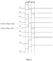
- FIG. 3 is a drive timing diagram of a microfluidic pixel driving circuit according to an embodiment of the present disclosure.
- the drive timing of the microfluidic pixel driving circuit includes a first period t 1 and a second period t 2 that are set in sequence.
- the enable level of the first scan signal G 1 is used to control the first write unit 11 to be turned on to write the first data signal S 1 to the pixel electrode, and the voltage of the first node Vp corresponding to the pixel electrode is increased.
- the enable level of the second scan signal G 2 is used to control the second write unit 12 to be turned on to write a first voltage value of the second data signal S 2 to the second terminal of the second capacitor C 2 , that is, to write the first voltage value of the second data signal S 2 to the second node V 2 .
- the disable level of the first scan signal G 1 is used to control the first write unit 11 to be turned off.
- the enable level of the second scan signal G 2 is used to control the second write unit 12 to be turned on to write a second voltage value of the second data signal S 2 to the second terminal of the second capacitor C 2 , that is, to write the second voltage value of the second data signal S 2 to the second node V 2 .
- the second voltage value is greater than the first voltage value.
- the voltage value of the second node V 2 is increased from the first voltage value to the second voltage value, the voltage of the second node V 2 is increased and fed to the first node Vp through the second capacitor C 2 , and the voltage of the first node Vp is increased so that the voltage of the pixel electrode is increased.
- the drive timing further includes a third period t 3 , where the third period t 3 is after the second period t 2 , and the second period t 2 is after the first period t 1 .
- the enable level of the third scan signal G 3 is used to control the third write unit 13 to be turned on to write a third voltage value of the third data signal S 3 to the second terminal of the third capacitor C 3 , that is, to write the third voltage value of the third data signal S 3 to the third node V 3 .
- the disable level of the first scan signal G 1 is used to control the first write unit 11 to be turned off
- the disable level of the second scan signal G 2 is used to control the second write unit 12 to be turned off
- the enable level of the third scan signal G 3 is used to control the third write unit 13 to be turned on to write a fourth voltage value of the third data signal S 3 to the second terminal of the third capacitor C 3 , that is, to write the fourth voltage value of the third data signal S 3 to the third node V 3 .
- the fourth voltage value is greater than the third voltage value.
- the voltage value of the third node V 3 is increased from the third voltage value to the fourth voltage value, the voltage of the third node V 3 is increased and fed to the first node Vp through the third capacitor C 3 and the second capacitor C 2 , and the voltage of the first node Vp is increased so that the voltage of the pixel electrode is increased.
- FIG. 4 is another drive timing diagram of a microfluidic pixel driving circuit according to an embodiment of the present disclosure.
- the disable level of the third scan signal G 3 is used to control the third write unit 13 to be turned off.
- the enable level of the third scan signal G 3 is used to control the third write unit 13 to be turned on to write the third voltage value of the third data signal S 3 to the second terminal of the third capacitor C 3 , that is, to write the third voltage value of the third data signal S 3 to the third node V 3 .
- FIG. 5 is another drive timing diagram of a microfluidic pixel driving circuit according to an embodiment of the present disclosure.
- the enable level of the third scan signal G 3 is used to control the third write unit 13 to be turned on to write the third voltage value of the third data signal S 3 to the second terminal of the third capacitor C 3 , that is, to write the third voltage value of the third data signal S 3 to the third node V 3 .
- the disable level of the third scan signal G 3 is used to control the third write unit 13 to be turned off.
- a capacitor C in an m-th boost module 111 of the n boost modules 111 is connected in series between a write unit 10 in the m-th boost module 111 and a write unit 10 in an (m ⁇ 1)-th boost module 111 , where 2 ⁇ m ⁇ n.
- a voltage V p,tn of the pixel electrode after n-stage boosting satisfies that
- V p , tn V SH + ⁇ 1 n ⁇ 1 C 1 ⁇ 1 i ⁇ 1 C j ⁇ ( V SH - V SL ) ,
- V p , t ⁇ 2 V S ⁇ H + C 2 C 1 + C 2 ⁇ ( V S ⁇ H - V S ⁇ L ) .
- V p , t ⁇ 3 V S ⁇ H + ( C 2 C 1 + C 2 + C 2 ⁇ C 3 C 1 ⁇ C 2 + C 2 ⁇ C 3 + C 1 ⁇ C 3 ) ⁇ ( V S ⁇ H - V S ⁇ L ) .
- V p , tn V SH + ⁇ 1 n ⁇ 1 C 1 ⁇ 1 i ⁇ 1 C j ⁇ ( V SH - V SL ) .
- a second terminal of the capacitor C in the m-th boost module 111 is electrically connected to the write unit 10 in the m-th boost module 111
- a first terminal of the capacitor C in the m-th boost module 111 is electrically connected to the write unit 10 in the (m ⁇ 1)-th boost module 111 , where 2 ⁇ m ⁇ n.
- a capacitor C in the m-th boost module 111 is connected in series between a write unit 10 in the m-th boost module 111 and a write unit 10 in the (m ⁇ 1)-th boost module 111 .
- a capacitor C in the higher-stage boost module 111 has a greater capacitance value.
- the capacitance value of the second capacitor C 2 is greater than the capacitance value of the first capacitor C 1
- the capacitance value of the third capacitor C 3 is greater than the capacitance value of the second capacitor C 2
- a capacitance value of the capacitor C in the m-th boost module 111 is greater than a capacitance value of a capacitor C in the (m ⁇ 1)-th boost module 111 , . . .
- a capacitance value of a capacitor C in the n-th boost module 111 is greater than a capacitance value of a capacitor C in an (n ⁇ 1)-th boost module 111 .
- the capacitor C in the m-th boost module 111 has a greater distance from the first node Vp than the capacitor C in the (m ⁇ 1)-th boost module 111 .
- the greater capacitance value needs to be set, to increase a voltage increment fed to the first node Vp, increase a voltage increment of the first node Vp, and increase the voltage of the pixel electrode.
- the second terminal of the capacitor C in the m-th boost module 111 is electrically connected to the write unit 10 in the m-th boost module 111
- the first terminal of the capacitor C in the m-th boost module 111 is electrically connected to the write unit 10 in the (m ⁇ 1)-th boost module 111 , where 2 ⁇ m ⁇ n.
- the write unit 10 includes a transistor, and the transistor includes the first transistor M 1 , the second transistor M 2 , and the third transistor M 3 .
- a transistor in the higher-stage boost module 111 has a greater channel width-to-length ratio.
- a channel width-to-length ratio of the second transistor M 2 is greater than a channel width-to-length ratio of the first transistor M 1
- a channel width-to-length ratio of the third transistor M 3 is greater than the channel width-to-length ratio of the second transistor M 2
- a channel width-to-length ratio of the transistor in the m-th boost module 111 is greater than a channel width-to-length ratio of a transistor in the (m ⁇ 1)-th boost module 111 , . . .
- a channel width-to-length ratio of a transistor in the n-th boost module 111 is greater than a channel width-to-length ratio of a transistor in the (n ⁇ 1)-th-stage boost module 111 .
- the transistor in the higher-stage boost module 111 is configured with the greater channel width-to-length ratio to adapt to the capacitance value and charging time of the capacitor C so that capacitors C with different capacitance values can complete a charging or discharging process in the same or similar time.
- the transistor is an n-type transistor, which is turned on at a high level and turned off at a low level.
- the high level is an enable level and the low level is a disable level.
- the transistor may be a p-type transistor, which is turned on at the low level and turned off at the high level.
- the low level is an enable level and the high level is a disable level.
- FIG. 6 is a top view illustrating the structure of a microfluidic substrate according to an embodiment of the present disclosure.
- FIG. 7 is a top view illustrating the structure of a pixel unit according to an embodiment of the present disclosure.
- FIG. 8 is a sectional view of the pixel unit of FIG. 7 taken along a direction AA′.
- the microfluidic substrate includes a substrate 20 and a pixel unit 100 on a side of the substrate 20 .
- the pixel unit 100 includes the microfluidic pixel driving circuit 110 in the preceding embodiments and a pixel electrode 120 .
- the microfluidic pixel driving circuit 110 is electrically connected to the pixel electrode 120 and provides a drive voltage for the pixel electrode 120 . Since the microfluidic pixel driving circuit 110 can implement multi-stage boosting, a voltage value of the pixel electrode 120 is increased.
- the microfluidic substrate includes a scan line unit 21 and a data line unit 22 .
- the data line unit 22 includes n data lines arranged along a first direction.
- the scan line unit 21 includes n scan lines arranged along a second direction. The first direction intersects the second direction.
- Each capacitor C of the n boost modules includes an upper plate C 01 and a lower plate C 02 . In a direction perpendicular to the substrate 20 , the lower plate C 02 is disposed between the substrate 20 and the upper plate C 01 , and the upper plate C 01 is disposed between the pixel electrode 120 and the lower plate C 02 .
- the upper plate C 01 is in the same layer as the data lines, and the lower plate C 02 is in the same layer as the scan lines.
- the upper plate C 01 of the capacitor C and the data lines can both be formed by using the same material in the same process, and the lower plate C 02 of the capacitor C and the scan lines both can be formed by using the same material in the same process, thereby saving manufacturing processes.
- the data line unit 22 includes three data lines arranged along the first direction.
- the scan line unit 21 includes three scan lines arranged along the second direction.
- the three scan lines in the scan line unit 21 are denoted as a first scan line 211 , a second scan line 212 , and a third scan line 213 , separately.
- the three data lines in the data line unit 22 are denoted as a first data line 221 , a second data line 222 , and a third data line 223 , separately.
- Multiple scan lines in multiple scan line units 21 may extend along the first direction and be arranged along the second direction, and multiple data lines in multiple data line units 22 may extend along the second direction and be arranged along the first direction.
- the microfluidic substrate includes a fixed potential line COM (not shown in FIG. 6 ).
- An upper plate C 01 of the first capacitor C 1 is electrically connected to the fixed potential line COM.
- a lower plate C 02 of the first capacitor C 1 is electrically connected to the pixel electrode 120 , and the lower plate C 02 of the first capacitor C 1 has the same voltage as the pixel electrode 120 .
- the upper plate C 01 of the first capacitor C 1 is disposed between the lower plate C 02 of the first capacitor C 1 and the pixel electrode 120 , the upper plate C 01 of the first capacitor C 1 and the lower plate C 02 of the first capacitor C 1 form a capacitor, and the upper plate C 01 of the first capacitor C 1 and the pixel electrode 120 form a capacitor, thereby increasing a capacitance value of the first capacitor C 1 .
- an area of the first capacitor C 1 can be reduced so that enough space is reserved for other elements such as a second capacitor C 2 , or an area of the pixel unit 100 can be reduced so that the number of pixel units 100 in a unit area can be increased, thereby increasing a pixel resolution.
- the upper plate C 01 of the first capacitor C 1 is in the same layer as the fixed potential line COM.
- the upper plate C 01 of the first capacitor C 1 and the fixed potential line COM can both be formed by using the same material in the same process, thereby saving the manufacturing processes.
- an upper plate C 01 of the second capacitor C 2 is electrically connected to the lower plate C 02 of the first capacitor C 1 . Since the lower plate C 02 of the first capacitor C 1 is electrically connected to the pixel electrode 120 , the upper plate C 01 of the second capacitor C 2 is electrically connected to the pixel electrode 120 . In other embodiments, a lower plate C 02 of the second capacitor C 2 may be electrically connected to the lower plate C 02 of the first capacitor C 1 .
- a lower plate C 02 of the third capacitor C 3 is electrically connected to the lower plate C 02 of the second capacitor C 2 .
- the lower plate C 02 of the third capacitor C 3 is in the same layer as the lower plate C 02 of the second capacitor C 2 , the lower plate C 02 of the third capacitor C 3 and the lower plate C 02 of the second capacitor C 2 may be formed in the same process, and when the lower plate C 02 of the third capacitor C 3 and the lower plate C 02 of the second capacitor C 2 are patterned, a conductive film between the lower plate C 02 of the third capacitor C 3 and the lower plate C 02 of the second capacitor C 2 may be retained as a connection line, thereby simplifying a manufacturing process.
- a transistor includes a semiconductor layer, a gate, a first electrode, and a second electrode.
- the gate of the transistor is in the same layer as the lower plate C 02 of the capacitor C
- the first electrode of the transistor and the second electrode of the transistor are in the same layer as the upper plate C 01 of the capacitor C.
- an upper plate C 01 of the third capacitor C 3 is electrically connected to a first electrode of a third transistor M 3 .
- the upper plate C 01 of the third capacitor C 3 is in the same layer as the first electrode of the third transistor M 3 , the upper plate C 01 of the third capacitor C 3 and the first electrode of the third transistor M 3 may be formed in the same process, and when the upper plate C 01 of the third capacitor C 3 and the first electrode of the third transistor M 3 are patterned, a conductive film between the upper plate C 01 of the third capacitor C 3 and the first electrode of the third transistor M 3 may be retained as a connection line, thereby simplifying a manufacturing process.
- the data lines include the first data line 221 providing a first data signal S 1 .
- a vertical projection of the first data line 221 on the substrate 20 is located between a vertical projection of the first capacitor C 1 on the substrate 20 and a vertical projection of the second capacitor C 2 on the substrate 20 .
- the microfluidic substrate further includes a connection line 30 and a bridge 40 , where the connection line 30 overlaps the first data line 221 in different layers, and a first terminal of the connection line 30 is electrically connected to the lower plate C 02 of the first capacitor C 1 .
- the bridge 40 is used to is used to connect a second terminal of the connection line 30 to the upper plate C 01 of the second capacitor C 2 .
- the upper plate C 01 of the second capacitor C 2 is electrically connected to the lower plate C 02 of the first capacitor C 1 through the bridge 40 and the connection line 30 .
- connection line 30 includes a first connection line 31 , where the first connection line 31 and the upper plate C 01 of the second capacitor C 2 are in different layers, and the first connection line 31 overlaps the first data line 221 in different layers.
- the bridge 40 includes a first bridge 41 connecting the first connection line 31 to the upper plate C 01 of the second capacitor C 2 .
- the data lines include the second data line 222 providing a second data signal S 2 .
- a vertical projection of the second data line 222 on the substrate 20 is located between the vertical projection of the second capacitor C 2 on the substrate 20 and a vertical projection of the third capacitor C 3 on the substrate 20 .
- the microfluidic substrate further includes a connection line 30 , where the connection line 20 overlaps the second data line 222 in different layers, and the connection line 30 is used to connect the lower plate C 02 of the second capacitor C 2 to the lower plate C 02 of the third capacitor C 3 .
- the lower plate C 02 of the third capacitor C 3 is electrically connected to the lower plate C 02 of the second capacitor C 2 through the connection line 30 .
- connection line 30 includes a second connection line 32 , where the second connection line 32 overlaps the second data line 222 in different layers.
- FIG. 9 is another top view illustrating the structure of a pixel unit according to an embodiment of the present disclosure.
- FIG. 10 is a sectional view of the pixel unit of FIG. 9 taken along a direction BB′.
- the scan lines include the first scan line 211 providing a first scan signal G 1 .
- a first write unit 11 includes a first transistor M 1 , where a gate of the first transistor M 1 is electrically connected to the first scan line 211 , and the first scan line 211 provides the first scan signal G 1 for the gate of the first transistor M 1 .
- a first electrode of the first transistor M 1 is electrically connected to the bridge 40 .
- the first electrode of the first transistor M 1 is electrically connected to the first bridge 41 and connected to the pixel electrode 120 through the first bridge 41 and the first connection line 31 .
- a second electrode of the first transistor M 1 is electrically connected to the first data line 221 in the same layer.
- FIG. 11 is another top view illustrating the structure of a pixel unit according to an embodiment of the present disclosure.
- FIG. 12 is a sectional view of the pixel unit of FIG. 11 taken along a direction CC′.
- the scan lines include the second scan line 212 providing a second scan signal G 2 .
- a second write unit 12 includes a second transistor M 2 , where a gate of the second transistor M 2 is electrically connected to the second scan line 212 , and the second scan line 212 provides the second scan signal G 2 for the gate of the second transistor M 2 .
- a second electrode of the second transistor M 2 is electrically connected to the second data line 222 in the same layer.
- the microfluidic substrate further includes a bridge 40 , where the bridge 40 is used to connect the connection line 30 to a first electrode of the second transistor M 2 .
- connection line 30 includes the second connection line 32 , where the second connection line 32 and the first electrode of the second transistor M 2 are in different layers, and the second connection line 32 overlaps the second data line 222 in different layers.
- the bridge 40 includes a second bridge 42 connecting the second connection line 32 to the first electrode of the second transistor M 2 .
- the data lines further include the third data line 223 providing a third data signal S 3 .
- a vertical projection of the third data line 223 on the substrate 20 is located on a side of the vertical projection of the third capacitor C 3 on the substrate 20 facing away from the vertical projection of the second capacitor C 2 on the substrate 20 .
- the vertical projection of the third capacitor C 3 on the substrate 20 is located between the vertical projection of the third data line 223 on the substrate 20 and the vertical projection of the second data line 222 on the substrate 20 .
- the scan lines include the third scan line 213 providing a third scan signal G 3 .
- a third write unit 13 includes the third transistor M 2 , where a gate of the third transistor M 3 is electrically connected to the third scan line 213 , and the third scan line 213 provides the third scan signal G 3 for the gate of the third transistor M 3 .
- the first electrode of the third transistor M 3 is electrically connected to the upper plate C 01 of the third capacitor C 3 in the same layer.
- a second electrode of the third transistor M 3 is electrically connected to the third data line 223 in the same layer.
- the bridge 40 is in the same layer as the pixel electrode 120 .
- the bridge 40 and the pixel electrode 120 can both be formed by using the same material in the same process, thereby saving the manufacturing processes.
- no new film needs to be provided for the bridge 40 , thereby reducing a thickness of the microfluidic substrate.
- the bridge 40 and the pixel electrode 120 are in the same layer, a shallow hole needs to be formed between the bridge 40 and the upper plate C 01 of the capacitor C, a deep hole needs to be formed between the bridge 40 and the lower plate C 02 of the capacitor C, and the deep hole and the shallow hole can be formed in the same photolithography process, thereby saving the manufacturing processes.
- the pixel electrode 120 is provided with an opening at the position of the bridge 40 , to prevent the pixel electrode 120 from being directly connected to the bridge 40 .
- the first bridge 41 since the first bridge 41 is electrically connected to the pixel electrode 120 through the first connection line 31 , the first bridge 41 is electrically connected to the pixel electrode 120 indirectly even if the first bridge 41 is not directly connected to the pixel electrode 120 .
- the second bridge 42 since the second bridge 42 is electrically connected to the lower plate C 02 of the second capacitor C 2 through the second connection line 32 , the second bridge 42 is electrically insulated from the pixel electrode 120 .
- FIG. 13 is another top view illustrating the structure of a pixel unit according to an embodiment of the present disclosure.
- FIG. 14 is a sectional view of the pixel unit of FIG. 13 taken along a direction DD′.
- the pixel electrode 120 is provided with no opening at the position of the first bridge 41 , and the first bridge 41 and the pixel electrode 120 are an integrated structure.
- the first bridge 41 may be understood as a position of a conductive film where the pixel electrode 120 is located for setting a via for the first connection line 31 .
- the pixel electrode 120 is directly connected to the first bridge 41 .
- the pixel electrode 120 needs to be provided with an opening at the position of the second bridge 42 , to ensure that the second bridge 42 is electrically insulated from the pixel electrode 120 .
- FIG. 15 is another top view illustrating the structure of a pixel unit according to an embodiment of the present disclosure.
- the filling pattern of the pixel electrode 120 in FIG. 15 is omitted and the outline of the pixel electrode 120 is illustrated only by an outer box, to prevent other films from being blocked by the pixel electrode 120 filled with the pattern.
- FIG. 16 is a sectional view of the pixel unit of FIG. 15 taken along a direction EE′.
- the bridge 40 and the pixel electrode 120 are in different layers.
- the bridge 40 is disposed between the upper plate C 01 of the capacitor C and the pixel electrode 120 . Since the bridge 40 and the pixel electrode 120 are in different layers, the bridge 40 may overlap the pixel electrode 120 in the direction perpendicular to the substrate 20 .
- the pixel electrode 120 is connected to the first connection line 31 through a via 50 .
- FIG. 17 is another top view illustrating the structure of a pixel unit according to an embodiment of the present disclosure.
- FIG. 18 is a sectional view of the pixel unit of FIG. 17 taken along a direction FF′.
- the bridge 40 is in the same layer as the data lines.
- the bridge 40 and the data lines can both be formed by using the same material in the same process, thereby saving the manufacturing processes.
- no new film needs to be provided for the bridge 40 , thereby reducing the thickness of the microfluidic substrate.
- the bridge 40 and the pixel electrode 120 are in different layers, the bridge 40 may overlap the pixel electrode 120 in the direction perpendicular to the substrate 20 .
- connection line 30 is in the same layer as the scan lines.
- the connection line 30 and the scan lines can both be formed by using the same material in the same process, thereby saving the manufacturing processes.
- no new film needs to be provided for the connection line 30 , thereby reducing the thickness of the microfluidic substrate.
- connection line 30 is in the same layer as the scan lines, the scan lines are in the same layer as the lower plate C 02 of the capacitor C, and the connection line 30 is in the same layer as the lower plate C 02 of the capacitor C so that when the connection line 30 is connected to the lower plate C 02 of the capacitor C, the connection line 30 is directly electrically connected to the lower plate C 02 of the capacitor C in the same layer without providing a bridge, the space originally used for providing the capacitor C is not occupied, and an area of the capacitor C is increased.
- the capacitance value of the capacitor C is set, the area of the pixel unit 100 can be reduced so that the number of pixel units 100 in a unit area can be increased, thereby increasing the pixel resolution.
- FIG. 19 is another top view illustrating the structure of a pixel unit according to an embodiment of the present disclosure.
- FIG. 20 is a sectional view of the pixel unit of FIG. 19 taken along a direction GG′.
- the connection line 30 is in the same layer as the pixel electrode 120 .
- the connection line 30 and the pixel electrode 120 can both be formed by using the same material in the same process, thereby saving the manufacturing processes.
- the pixel electrode 120 is provided with an opening at the position of the connection line 30 .
- the first connection line 31 since the first connection line 31 is electrically connected to the pixel electrode 120 , the first connection line 31 is electrically connected to the pixel electrode 120 .
- the second connection line 32 since the second connection line 32 is electrically connected to the lower plate C 02 of the second capacitor C 2 , the second connection line 32 is electrically insulated from the pixel electrode 120 .
- the microfluidic substrate includes the fixed potential line COM, the fixed potential line COM extend along the second direction, and the fixed potential line COM is in the same layer as the data lines (including the first data line 221 and the second data line 222 ).
- the fixed potential line COM is electrically connected to the upper plate C 01 of the first capacitor C 1 in the same layer.
- FIG. 21 is another top view illustrating the structure of a pixel unit according to an embodiment of the present disclosure.
- FIG. 22 is a sectional view of the pixel unit of FIG. 21 taken along a direction HH′.
- the microfluidic substrate includes the fixed potential line COM.
- the capacitor C includes the first capacitor C 1 , and the lower plate C 02 of the first capacitor C 1 is electrically connected to the fixed potential line COM in the same layer.
- the upper plate C 01 of the first capacitor C 1 is electrically connected to the pixel electrode 120 .
- the fixed potential line COM extend along the first direction, and the fixed potential line COM is in the same layer as the scan lines (including the first scan line 211 and the second scan line 212 ).
- the fixed potential line COM is electrically connected to the lower plate C 02 of the first capacitor C 1 in the same layer.
- the upper plate C 01 of the first capacitor C 1 is electrically connected to the fixed potential line COM
- the upper plate C 01 of the second capacitor C 2 is electrically connected to the lower plate C 02 of the first capacitor C 1
- the lower plate C 02 of the third capacitor C 3 is electrically connected to the lower plate C 02 of the second capacitor C 2
- the upper plate C 01 of the third capacitor C 3 is electrically connected to the first electrode of the third transistor M 3 .
- the upper plate C 01 of the first capacitor C 1 is electrically connected to the fixed potential line COM
- the lower plate C 02 of the second capacitor C 2 is electrically connected to the lower plate C 02 of the first capacitor C 1
- the lower plate C 02 of the third capacitor C 3 is electrically connected to the upper plate C 01 of the second capacitor C 2
- the upper plate C 01 of the third capacitor C 3 is electrically connected to the first electrode of the third transistor M 3 .
- the lower plate C 02 of the third capacitor C 3 instead of the upper plate C 01 of the third capacitor C 3 may be electrically connected to the first electrode of the third transistor M 3 .
- FIG. 23 is another top view illustrating the structure of a pixel unit according to an embodiment of the present disclosure.
- FIG. 24 is a sectional view of the pixel unit of FIG. 23 taken along a direction II′.
- the microfluidic substrate includes the fixed potential line COM.
- the capacitor C includes the first capacitor C 1 , the second capacitor C 2 , and the third capacitor C 3 .
- the upper plate C 01 of the first capacitor C 1 is electrically connected to the fixed potential line COM
- the upper plate C 01 of the second capacitor C 2 is electrically connected to the lower plate C 02 of the first capacitor C 1
- the upper plate C 01 of the third capacitor C 3 is electrically connected to the lower plate C 02 of the second capacitor C 2 .
- the bridge 40 includes a third bridge 43 connecting the lower plate C 02 of the third capacitor C 3 to the first electrode of the third transistor M 3 .
- the microfluidic substrate includes the scan line unit 21 .
- the scan line unit 21 includes the n scan lines arranged along the second direction. Along the second direction, all the scan lines in the same scan line unit 21 are disposed on the same side of the capacitor C.
- the scan line unit 21 includes the first scan line 211 , the second scan line 212 , and the third scan line 213 .
- the first scan line 211 , the second scan line 212 , and the third scan line 213 are disposed on the same side of the capacitor C (including the first capacitor C 1 , the second capacitor C 2 , and the third capacitor C 3 ). In this manner, the openings of the pixel electrode 120 are arranged correspondingly on the same side of the capacitor C.
- FIG. 25 is another top view illustrating the structure of a pixel unit according to an embodiment of the present disclosure.
- each of the scan lines includes a capacitor avoidance portion 210 , where a vertical projection of the capacitor avoidance portion 210 on the substrate 20 does not overlap a vertical projection of a respective capacitor C on the substrate 20 . That is to say, the vertical projection of the capacitor avoidance portion 210 on the substrate 20 does not overlap the vertical projection of the capacitor C on the substrate 20 .
- the capacitor avoidance portion 210 is provided for reserving a space for the position of the capacitor C towards the scan lines. A distance between adjacent scan lines corresponding to the position of the capacitor C is reduced, thereby increasing the area of the capacitor C.
- the capacitance value of the capacitor C is set, the area of the pixel unit 100 can be reduced so that the number of pixel units 100 in a unit area can be increased, thereby increasing the pixel resolution.
- the microfluidic substrate includes the scan line unit 21 and the data line unit 22 .
- the data line unit 22 includes the n data lines arranged along the first direction.
- the scan line unit 21 includes the n scan lines arranged along the second direction.
- Microfluidic pixel driving circuits 110 arranged in one row along the first direction are electrically connected to the same scan line unit 21
- microfluidic pixel driving circuits 110 arranged in one column along the second direction are electrically connected to the same data line unit 22 .
- the pixel unit 100 (including the microfluidic pixel driving circuit 110 and the pixel electrode 120 ) is provided at an intersection between the scan line unit 21 and the data line unit 22 .
- FIG. 26 is another top view illustrating the structure of a microfluidic substrate according to an embodiment of the present disclosure.
- the microfluidic substrate includes multiple scan selection circuits 51 , multiple scan source signal lines 52 , and n scan control signal lines 53 .
- Each scan selection circuit 51 includes n scan selection units 510 .
- First terminals of the n scan selection units 510 in the same scan selection circuit 51 are electrically connected to the same scan source signal line 52
- control terminals of the n scan selection units 510 are electrically connected in one-to-one correspondence to the n scan control signal lines 53
- second terminals of the n scan selection units 510 are electrically connected in one-to-one correspondence to the n scan lines.
- a scan selection unit 510 When a scan selection unit 510 is turned on under the control of an enable level of a scan control signal line 53 connected to the scan selection unit 510 , an electrical signal on the scan source signal line 52 is transmitted to a scan line connected to the scan selection unit 510 .
- the scan selection circuits 51 and the scan control signal lines 53 are provided, the same scan source signal line 52 is controlled by the scan control signal lines 53 to provide electrical signals for different scan lines separately, and the number of scan source signal lines 52 is 1/n of the number of scan lines, thereby reducing the number of scan source signal lines 52 and reducing the number of ports of a driver chip.
- the microfluidic substrate includes three scan control signal lines 53 , and the three scan control signal lines 53 are denoted as a first scan control signal line 531 , a second scan control signal line 532 , and a third scan control signal line 533 , separately.
- the scan selection circuit 51 includes three scan selection units 510 .
- a control terminal of a first scan selection circuit 510 is electrically connected to the first scan control signal line 531
- a first terminal of the first scan selection unit 510 is electrically connected to the scan source signal line 52
- a second terminal of the first scan selection unit 510 is electrically connected to the first scan line 211 .
- a control terminal of a second scan selection circuit 510 is electrically connected to the second scan control signal line 532 , a first terminal of the second scan selection unit 510 is electrically connected to the scan source signal line 52 , and a second terminal of the second scan selection unit 510 is electrically connected to the second scan line 212 .
- a control terminal of a third scan selection circuit 510 is electrically connected to the third scan control signal line 533 , a first terminal of the third scan selection unit 510 is electrically connected to the scan source signal line 52 , and a second terminal of the third scan selection unit 510 is electrically connected to the third scan line 213 .
- the microfluidic substrate includes multiple data selection circuits 61 , multiple data source signal lines 62 , and n data control signal lines 63 .
- Each data selection circuit 61 includes n data selection units 610 .
- First terminals of the n data selection units 610 in the same data selection circuit 61 are electrically connected to the same data source signal line 62
- control terminals of the n data selection units 610 are electrically connected in one-to-one correspondence to the n data control signal lines 63
- second terminals of the n data selection units 610 are electrically connected in one-to-one correspondence to the n data lines.
- a data selection unit 610 When a data selection unit 610 is turned on under the control of an enable level of a data control signal line 63 connected to the data selection unit 610 , an electrical signal on the data source signal line 62 is transmitted to a data line connected to the data selection unit 610 .
- the data selection circuits 61 and the data control signal lines 63 are provided, the same data source signal line 62 is controlled by the data control signal lines 63 to provide electrical signals for different data lines separately, and the number of data source signal lines 62 is 1/n of the number of data lines, thereby reducing the number of data source signal lines 62 and reducing the number of ports of the driver chip.
- the microfluidic substrate includes three data control signal lines 63 , and the three data control signal lines 63 are denoted as a first data control signal line 631 , a second data control signal line 632 , and a third data control signal line 633 , separately.
- the data selection circuit 61 includes three data selection units 610 .
- a control terminal of a first data selection circuit 610 is electrically connected to the first data control signal line 631
- a first terminal of the first data selection unit 610 is electrically connected to the data source signal line 62
- a second terminal of the first data selection unit 610 is electrically connected to the first data line 221 .
- a control terminal of a second data selection circuit 610 is electrically connected to the second data control signal line 632 , a first terminal of the second data selection unit 610 is electrically connected to the data source signal line 62 , and a second terminal of the second data selection unit 610 is electrically connected to the second data line 222 .
- a control terminal of a third data selection circuit 610 is electrically connected to the third data control signal line 633 , a first terminal of the third data selection unit 610 is electrically connected to the data source signal line 62 , and a second terminal of the third data selection unit 610 is electrically connected to the third data line 223 .
- FIG. 27 is a drive timing diagram of a microfluidic substrate according to an embodiment of the present disclosure.
- a drive timing includes a first period t 1 and a second period t 2 that are set in sequence.
- an enable level of the first scan control signal line 531 is used to control the scan selection unit 510 connected to the first scan control signal line 531 to be turned on to transmit an enable level of the scan source signal line 52 to the first scan line 211
- an enable level of the second scan control signal line 532 is used to control the scan selection unit 510 connected to the second scan control signal line 532 to be turned on to transmit the enable level of the scan source signal line 52 to the second scan line 212 .
- a disable level of the first scan control signal line 531 is used to control the scan selection unit 510 connected to the first scan control signal line 531 to be turned off
- the enable level of the second scan control signal line 532 is used to control the scan selection unit 510 connected to the second scan control signal line 532 to be turned on to transmit the enable level of the scan source signal line 52 to the second scan line 212 .
- the enable level of the scan source signal line 52 is transmitted to the first scan line 211 , and the first scan line 211 transmits an enable level of the first scan signal G 1 .
- the enable level of the scan source signal line 52 is transmitted to the second scan line 212 , and the second scan line 212 transmits an enable level of the second scan signal G 2 .
- the drive timing further includes a third period t 3 , where the third period t 3 is after the second period t 2 , and the second period t 2 is after the first period t 1 .
- an enable level of the third scan control signal line 533 is used to control the scan selection unit 510 connected to the third scan control signal line 533 to be turned on to transmit the enable level of the scan source signal line 52 to the third scan line 213 .
- the disable level of the first scan control signal line 531 is used to control the scan selection unit 510 connected to the first scan control signal line 531 to be turned off
- a disable level of the second scan control signal line 532 is used to control the scan selection unit 510 connected to the second scan control signal line 532 to be turned off
- the enable level of the third scan control signal line 533 is used to control the scan selection unit 510 connected to the third scan control signal line 533 to be turned on to transmit the enable level of the scan source signal line 52 to the third scan line 213 .
- the enable level of the scan source signal line 52 is transmitted to the third scan line 213 , and the third scan line 213 transmits an enable level of the third scan signal G 3 .
- a disable level of the third scan control signal line 533 is used to control the scan selection unit 510 connected to the third scan control signal line 533 to be turned off.
- the enable level of the third scan control signal line 533 is used to control the scan selection unit 510 connected to the third scan control signal line 533 to be turned on to transmit the enable level of the scan source signal line 52 to the third scan line 213 .
- the enable level of the third scan control signal line 533 is used to control the scan selection unit 510 connected to the third scan control signal line 533 to be turned on to transmit the enable level of the scan source signal line 52 to the third scan line 213 .
- the disable level of the third scan control signal line 533 is used to control the scan selection unit 510 connected to the third scan control signal line 533 to be turned off.
- the drive timing of the third scan signal G 3 shown in FIG. 5 is formed.
- the multiple scan source signal lines 52 include a first scan source signal line 521 , a second scan source signal line 522 , and a third scan source signal line 523 .
- An enable level of the first scan source signal line 521 , an enable level of the second scan source signal line 522 , and an enable level of the third scan source signal line 523 occur in sequence.
- FIG. 28 is another drive timing diagram of a microfluidic substrate according to an embodiment of the present disclosure.
- the drive timing includes the first period t 1 and the second period t 2 that are set in sequence.
- an enable level of the first data control signal line 631 is used to control the data selection unit 610 connected to the first data control signal line 631 to be turned on to transmit an enable level of the data source signal line 62 to the first data line 221
- a disable level of the second data control signal line 632 is used to control the data selection unit 610 connected to the second data control signal line 632 to be turned off.
- a disable level of the first data control signal line 631 is used to control the data selection unit 610 connected to the first data control signal line 631 to be turned off, and an enable level of the second data control signal line 632 is used to control the data selection unit 610 connected to the second data control signal line 632 to be turned on to transmit the enable level of the data source signal line 62 to the second data line 222 .
- the enable level of the data source signal line 62 is transmitted to the first data line 221 , and the first data line 221 transmits an enable level of the first data signal S 1 .
- the enable level of the data source signal line 62 is transmitted to the second data line 222 , and the second data line 222 transmits an enable level of the second data signal S 2 .
- the drive timing further includes the third period t 3 , where the third period t 3 is after the second period t 2 , and the second period t 2 is after the first period t 1 .
- a disable level of the third data control signal line 633 is used to control the data selection unit 610 connected to the third data control signal line 633 to be turned off.
- the disable level of the first data control signal line 631 is used to control the data selection unit 610 connected to the first data control signal line 631 to be turned off
- the disable level of the second data control signal line 632 is used to control the data selection unit 610 connected to the second data control signal line 632 to be turned off
- an enable level of the third data control signal line 633 is used to control the data selection unit 610 connected to the third data control signal line 633 to be turned on to transmit the enable level of the data source signal line 62 to the third data line 223 .
- the enable level of the data source signal line 62 is transmitted to the third data line 223 , and the third data line 223 transmits an enable level of the third data signal S 3 .
- the multiple data source signal lines 62 include a first data source signal line 621 , a second data source signal line 622 , and a third data source signal line 623 .
- An enable level of the first data source signal line 621 , an enable level of the second data source signal line 622 , and an enable level of the third data source signal line 623 occur in sequence.
- FIG. 29 is a sectional view illustrating the structure of a microfluidic chip according to an embodiment of the present disclosure.
- the microfluidic chip includes a microfluidic substrate 01 , an opposing substrate 02 , and a channel layer 03 .
- the channel layer 03 is disposed between the opposing substrate 02 and the microfluidic substrate 01 and used for accommodating a droplet 71 .
- the microfluidic substrate 01 includes a first hydrophobic layer 73 disposed between a pixel electrode 120 and the channel layer 03 .
- the opposing substrate 02 includes an opposing substrate 77 , an opposing electrode 76 , and a second hydrophobic layer 75 , where the opposing electrode 76 is disposed between the opposing substrate 77 and the second hydrophobic layer 75 , and the second hydrophobic layer 75 is disposed between the opposing electrode 76 and the channel layer 03 .
- An electric field for driving the droplet 71 to move is formed between the opposing substrate 02 and the pixel electrode 120 .
- the opposing electrode 76 may be grounded. In another embodiment, the opposing electrode 80 may be electrically connected to a fixed potential line COM.
- the channel layer 03 includes a hydrophobic oil droplet 72 and a spacer layer 74 , where the spacer layer 74 is disposed between the microfluidic substrate 01 and the opposing substrate 02 , the spacer layer 74 forms a closed space with the microfluidic substrate 01 and the opposing substrate 02 , and the closed space is used for accommodating the droplet 71 and the hydrophobic oil droplet 72 .
- the hydrophobic oil droplet 72 functions as a lubricant to facilitate the movement of the droplet 71 .
- the hydrophobic oil droplet 72 wraps the droplet 71 to prevent the volatilization of the droplet 71 .
Landscapes
- Engineering & Computer Science (AREA)
- Physics & Mathematics (AREA)
- Computer Hardware Design (AREA)
- General Physics & Mathematics (AREA)
- Theoretical Computer Science (AREA)
- Control Of Indicators Other Than Cathode Ray Tubes (AREA)
Abstract
Description
-
- where VSH denotes a high-level data signal and VSL denotes a low-level data signal.
-
- where Vp,t1 denotes the voltage value of the first node Vp in the first period t1, V2,t1 denotes the voltage value of the second node V2 in the first period t1, and V3,t1 denotes the voltage value of the third node V3 in the first period t1.
-
- where Vp,t2 denotes the voltage value of the first node Vp in the second period t2, V2,t2 denotes the voltage value of the second node V2 in the second period t2, V3,t2 denotes the voltage value of the third node V3 in the second period t2, C1 denotes a capacitance value of the first capacitor C1, and C2 denotes a capacitance value of the second capacitor C2.
where Vp,t3 denotes the voltage value of the first node Vp in the third period t3, V2,t3 denotes the voltage value of the second node V2 in the third period t3, V3,t3 denotes the voltage value of the third node V3 in the third period t3, and C3 denotes a capacitance value of the third capacitor C3.
Claims (16)
Applications Claiming Priority (2)
| Application Number | Priority Date | Filing Date | Title |
|---|---|---|---|
| CN202211412131.1 | 2022-11-11 | ||
| CN202211412131.1A CN115631729B (en) | 2022-11-11 | 2022-11-11 | Microfluidic pixel driving circuit, microfluidic substrate and microfluidic chip |
Publications (2)
| Publication Number | Publication Date |
|---|---|
| US20240071325A1 US20240071325A1 (en) | 2024-02-29 |
| US12307990B2 true US12307990B2 (en) | 2025-05-20 |
Family
ID=84910536
Family Applications (1)
| Application Number | Title | Priority Date | Filing Date |
|---|---|---|---|
| US18/387,304 Active US12307990B2 (en) | 2022-11-11 | 2023-11-06 | Microfluidic pixel driving circuit, microfluidic substrate, and microfluidic chip |
Country Status (2)
| Country | Link |
|---|---|
| US (1) | US12307990B2 (en) |
| CN (1) | CN115631729B (en) |
Citations (4)
| Publication number | Priority date | Publication date | Assignee | Title |
|---|---|---|---|---|
| CN206313448U (en) | 2016-11-10 | 2017-07-07 | 国家电网公司 | A kind of stagewise DC voltage means of active gulation for flexible DC power transmission |
| US20200316591A1 (en) * | 2019-04-04 | 2020-10-08 | Shanghai Avic Opto Electronics Co., Ltd. | Drive circuit and drive method thereof, and panel and drive method thereof |
| US20200316590A1 (en) * | 2019-04-04 | 2020-10-08 | Shanghai Avic Opto Electronics Co., Ltd. | Drive circuit and drive method thereof, and panel and drive method thereof |
| CN113674706A (en) | 2021-08-30 | 2021-11-19 | 上海天马微电子有限公司 | Driving circuit, driving method and microfluidic panel thereof |
Family Cites Families (3)
| Publication number | Priority date | Publication date | Assignee | Title |
|---|---|---|---|---|
| CN109584812B (en) * | 2019-01-03 | 2021-08-06 | 京东方科技集团股份有限公司 | Driving circuit of microfluidic device electrode, microfluidic device and driving method |
| CN110687953A (en) * | 2019-10-29 | 2020-01-14 | 上海天马微电子有限公司 | Driving circuit and driving method thereof, microfluidic substrate and microfluidic device |
| CN114677977B (en) * | 2022-03-10 | 2024-04-09 | 广东奥素液芯微纳科技有限公司 | Micro-fluidic pixel circuit and chip based on phase inverter |
-
2022
- 2022-11-11 CN CN202211412131.1A patent/CN115631729B/en active Active
-
2023
- 2023-11-06 US US18/387,304 patent/US12307990B2/en active Active
Patent Citations (4)
| Publication number | Priority date | Publication date | Assignee | Title |
|---|---|---|---|---|
| CN206313448U (en) | 2016-11-10 | 2017-07-07 | 国家电网公司 | A kind of stagewise DC voltage means of active gulation for flexible DC power transmission |
| US20200316591A1 (en) * | 2019-04-04 | 2020-10-08 | Shanghai Avic Opto Electronics Co., Ltd. | Drive circuit and drive method thereof, and panel and drive method thereof |
| US20200316590A1 (en) * | 2019-04-04 | 2020-10-08 | Shanghai Avic Opto Electronics Co., Ltd. | Drive circuit and drive method thereof, and panel and drive method thereof |
| CN113674706A (en) | 2021-08-30 | 2021-11-19 | 上海天马微电子有限公司 | Driving circuit, driving method and microfluidic panel thereof |
Also Published As
| Publication number | Publication date |
|---|---|
| CN115631729B (en) | 2024-06-11 |
| US20240071325A1 (en) | 2024-02-29 |
| CN115631729A (en) | 2023-01-20 |
Similar Documents
| Publication | Publication Date | Title |
|---|---|---|
| US12232385B2 (en) | Display substrate and display panel | |
| US11189227B1 (en) | Display panel, driving method thereof, and display device | |
| US20240312419A1 (en) | Display substrate | |
| CN115398528B (en) | Display panel and display device | |
| US11263960B2 (en) | Display panel, driving method and display device | |
| US11900873B2 (en) | Display panels, methods of driving the same, and display devices | |
| US10210836B2 (en) | Gate driver and display device using the same | |
| US11250786B2 (en) | Array substrate, display panel and display apparatus | |
| US6982568B2 (en) | Image display device having inspection terminal | |
| CN108713225B (en) | Active matrix substrate and liquid crystal display device having active matrix substrate | |
| US20180047316A1 (en) | Array substrate, electronic paper display panel and driving method thereof | |
| US6897841B2 (en) | Liquid crystal display device and electronic apparatus comprising it | |
| US8284156B2 (en) | Electrophoretic display device employing organic thin film transistors, driving method for driving circuits of the electrophoretic display device, and electronic apparatus including the electrophoretic display device | |
| US11315523B2 (en) | Emission controller, driving method, and display device | |
| US11935444B2 (en) | Detection circuit, driving circuit, and display panel and driving method therefor | |
| US12307990B2 (en) | Microfluidic pixel driving circuit, microfluidic substrate, and microfluidic chip | |
| CN118197225A (en) | Display panel, gate driving circuit, shift register and driving method thereof | |
| US12211454B2 (en) | Driving circuit, driving method, display substrate and display device with node control circuit for controlling potential of node | |
| US20240386856A1 (en) | Display panel, method for driving a display panel, and display device | |
| US7015985B2 (en) | Liquid crystal display array and liquid crystal display panel | |
| JPS62123427A (en) | Active matrix liquid crystal display element and its production | |
| CN117270270A (en) | Array substrate, touch display panel and display device | |
| US10814324B2 (en) | AM-EWOD array element circuitry with shared sensor components | |
| US20260100170A1 (en) | Display device | |
| US20230221605A1 (en) | Semiconductor device |
Legal Events
| Date | Code | Title | Description |
|---|---|---|---|
| AS | Assignment |
Owner name: SHANGHAI TIANMA MICROELECTRONICS CO., LTD., CHINA Free format text: ASSIGNMENT OF ASSIGNORS INTEREST;ASSIGNORS:ZHANG, KAIDI;LIN, BAIQUAN;BAI, YUNFEI;AND OTHERS;REEL/FRAME:065471/0074 Effective date: 20230105 |
|
| FEPP | Fee payment procedure |
Free format text: ENTITY STATUS SET TO UNDISCOUNTED (ORIGINAL EVENT CODE: BIG.); ENTITY STATUS OF PATENT OWNER: LARGE ENTITY |
|
| STPP | Information on status: patent application and granting procedure in general |
Free format text: DOCKETED NEW CASE - READY FOR EXAMINATION |
|
| STPP | Information on status: patent application and granting procedure in general |
Free format text: NON FINAL ACTION MAILED |
|
| STPP | Information on status: patent application and granting procedure in general |
Free format text: RESPONSE TO NON-FINAL OFFICE ACTION ENTERED AND FORWARDED TO EXAMINER |
|
| STPP | Information on status: patent application and granting procedure in general |
Free format text: NOTICE OF ALLOWANCE MAILED -- APPLICATION RECEIVED IN OFFICE OF PUBLICATIONS |
|
| STCF | Information on status: patent grant |
Free format text: PATENTED CASE |