US12302567B2 - Three-dimensional memory device and manufacturing method thereof - Google Patents
Three-dimensional memory device and manufacturing method thereof Download PDFInfo
- Publication number
- US12302567B2 US12302567B2 US17/703,893 US202217703893A US12302567B2 US 12302567 B2 US12302567 B2 US 12302567B2 US 202217703893 A US202217703893 A US 202217703893A US 12302567 B2 US12302567 B2 US 12302567B2
- Authority
- US
- United States
- Prior art keywords
- hole
- width
- stack
- mask
- opening
- Prior art date
- Legal status (The legal status is an assumption and is not a legal conclusion. Google has not performed a legal analysis and makes no representation as to the accuracy of the status listed.)
- Active, expires
Links
Images


Classifications
-
- H—ELECTRICITY
- H10—SEMICONDUCTOR DEVICES; ELECTRIC SOLID-STATE DEVICES NOT OTHERWISE PROVIDED FOR
- H10B—ELECTRONIC MEMORY DEVICES
- H10B43/00—EEPROM devices comprising charge-trapping gate insulators
- H10B43/30—EEPROM devices comprising charge-trapping gate insulators characterised by the memory core region
-
- H—ELECTRICITY
- H10—SEMICONDUCTOR DEVICES; ELECTRIC SOLID-STATE DEVICES NOT OTHERWISE PROVIDED FOR
- H10B—ELECTRONIC MEMORY DEVICES
- H10B41/00—Electrically erasable-and-programmable ROM [EEPROM] devices comprising floating gates
- H10B41/10—Electrically erasable-and-programmable ROM [EEPROM] devices comprising floating gates characterised by the top-view layout
-
- H—ELECTRICITY
- H10—SEMICONDUCTOR DEVICES; ELECTRIC SOLID-STATE DEVICES NOT OTHERWISE PROVIDED FOR
- H10B—ELECTRONIC MEMORY DEVICES
- H10B41/00—Electrically erasable-and-programmable ROM [EEPROM] devices comprising floating gates
- H10B41/20—Electrically erasable-and-programmable ROM [EEPROM] devices comprising floating gates characterised by three-dimensional [3D] arrangements, e.g. with cells on different height levels
- H10B41/23—Electrically erasable-and-programmable ROM [EEPROM] devices comprising floating gates characterised by three-dimensional [3D] arrangements, e.g. with cells on different height levels with source and drain on different levels, e.g. with sloping channels
- H10B41/27—Electrically erasable-and-programmable ROM [EEPROM] devices comprising floating gates characterised by three-dimensional [3D] arrangements, e.g. with cells on different height levels with source and drain on different levels, e.g. with sloping channels the channels comprising vertical portions, e.g. U-shaped channels
-
- H—ELECTRICITY
- H10—SEMICONDUCTOR DEVICES; ELECTRIC SOLID-STATE DEVICES NOT OTHERWISE PROVIDED FOR
- H10B—ELECTRONIC MEMORY DEVICES
- H10B41/00—Electrically erasable-and-programmable ROM [EEPROM] devices comprising floating gates
- H10B41/50—Electrically erasable-and-programmable ROM [EEPROM] devices comprising floating gates characterised by the boundary region between the core region and the peripheral circuit region
-
- H—ELECTRICITY
- H10—SEMICONDUCTOR DEVICES; ELECTRIC SOLID-STATE DEVICES NOT OTHERWISE PROVIDED FOR
- H10B—ELECTRONIC MEMORY DEVICES
- H10B43/00—EEPROM devices comprising charge-trapping gate insulators
- H10B43/10—EEPROM devices comprising charge-trapping gate insulators characterised by the top-view layout
-
- H—ELECTRICITY
- H10—SEMICONDUCTOR DEVICES; ELECTRIC SOLID-STATE DEVICES NOT OTHERWISE PROVIDED FOR
- H10B—ELECTRONIC MEMORY DEVICES
- H10B43/00—EEPROM devices comprising charge-trapping gate insulators
- H10B43/20—EEPROM devices comprising charge-trapping gate insulators characterised by three-dimensional [3D] arrangements, e.g. with cells on different height levels
- H10B43/23—EEPROM devices comprising charge-trapping gate insulators characterised by three-dimensional [3D] arrangements, e.g. with cells on different height levels with source and drain on different levels, e.g. with sloping channels
- H10B43/27—EEPROM devices comprising charge-trapping gate insulators characterised by three-dimensional [3D] arrangements, e.g. with cells on different height levels with source and drain on different levels, e.g. with sloping channels the channels comprising vertical portions, e.g. U-shaped channels
-
- H—ELECTRICITY
- H10—SEMICONDUCTOR DEVICES; ELECTRIC SOLID-STATE DEVICES NOT OTHERWISE PROVIDED FOR
- H10B—ELECTRONIC MEMORY DEVICES
- H10B43/00—EEPROM devices comprising charge-trapping gate insulators
- H10B43/40—EEPROM devices comprising charge-trapping gate insulators characterised by the peripheral circuit region
-
- H—ELECTRICITY
- H10—SEMICONDUCTOR DEVICES; ELECTRIC SOLID-STATE DEVICES NOT OTHERWISE PROVIDED FOR
- H10B—ELECTRONIC MEMORY DEVICES
- H10B43/00—EEPROM devices comprising charge-trapping gate insulators
- H10B43/50—EEPROM devices comprising charge-trapping gate insulators characterised by the boundary region between the core and peripheral circuit regions
Definitions
- Various embodiments generally relate to a semiconductor technology, and particularly, to a three-dimensional memory device and a method of manufacturing a three-dimensional memory device.
- a memory device with a two-dimensional or planar structure has been developed to store more data in the same area by using a fine patterning process.
- the line width of a circuit is narrowed due to the demand for high integration, interference between memory cells increases and causes various limitations such as degradation in performance.
- an increase in manufacturing cost is inevitable because of expensive equipment that is required to pattern increasingly narrow fine lines.
- a three-dimensional memory device has advantages in that a larger capacity may be realized within the same area by stacking memory cells in a vertical direction, thereby increasing the number of stacks through and providing high performance and excellent power efficiency.
- the degree of integration may be increased by increasing the number of electrode layers (word lines) to be stacked.
- electrode layers word lines
- contacts need to be coupled to each of the electrode layers, and various technologies are being developed to this end.
- Various embodiments are directed to a three-dimensional memory device and a manufacturing method thereof, capable of preventing failures in which the electrode layers are disconnected due to wide contact holes.
- a method for manufacturing a three-dimensional memory device may include: forming a through hole that passes through a stack including a plurality of first material layers and a plurality of second material layers alternately stacked on a substrate in a vertical direction; forming a mask to fill the through hole and to cover the stack; forming an opening that passes vertically through the mask and that aligns with a center portion of the through hole; expanding, in a horizontal direction, the opening in the mask disposed on the stack to expose the through hole and a portion of a top surface of the stack around the through hole; and partially etching the stack exposed by the opening.
- a method for manufacturing a three-dimensional memory device may include: forming a first through hole and a second through hole that pass through a stack including a plurality of first material layers and a plurality of second material layers alternately stacked on a substrate in a vertical direction; forming a first mask that fills the first and second through holes and covers the stack; forming a first opening that passes through the first mask at a center portion of the first through hole; expanding the first opening in the first mask in a horizontal direction to expose the first through hole and a top surface of the stack around the first through hole; partially etching the stack exposed by the expanded first opening; forming a second mask that fills the first and second through holes and covers the stack; forming second openings that pass through the first mask at a center portion of the first through hole and a center portion of the second through hole, respectively; expanding the second openings in the second mask in the horizontal direction to expose the partially expanded first through hole and a top surface of the stack around the partially expanded first through hole and to expose the second through
- a three-dimensional memory device may include: an electrode structure including a plurality of electrode layers and a plurality of interlayer dielectric layers which are alternately stacked on a substrate in a vertical direction; and a plurality of through holes, passing through the electrode structure in the vertical direction, that each include at least a first portion and a second portion having a different width, and pad regions are disposed on a surface of an electrode layer at the top of the first portion.
- FIG. 1 is a view schematically illustrating a three-dimensional memory device in accordance with an embodiment of the present disclosure.
- FIG. 2 is a top view illustrating a part of a three-dimensional memory device in accordance with an embodiment of the present disclosure.
- FIG. 3 is a cross-sectional view taken along the line A-A′ of FIG. 2 .
- FIGS. 4 A to 4 D are enlarged top views illustrating first to fourth through holes of FIG. 2 .
- FIGS. 5 A to 5 D are enlarged cross-sectional views illustrating the first to fourth through holes of FIG. 3 .
- FIG. 6 is a cross-sectional view after initial through holes of a three-dimensional memory device in accordance with an embodiment of the present disclosure are formed.
- FIGS. 7 A to 7 M are cross-sectional views illustrating process steps for forming through holes of a three-dimensional memory device in accordance with an embodiment of the present disclosure.
- FIGS. 8 A to 8 M are top views illustrating the process steps for forming the through holes of a three-dimensional memory device in accordance with an embodiment of the present disclosure.
- FIGS. 9 A to 9 F are cross-sectional views illustrating process steps for manufacturing a three-dimensional memory device in a comparative example.
- FIG. 10 is a top view illustrating through holes of the three-dimensional memory device in a comparative example.
- FIG. 11 is a block diagram illustrating a three-dimensional memory device in accordance with an embodiment of the present disclosure.
- FIG. 12 is a block diagram schematically illustrating a memory system including a three-dimensional memory device in accordance with an embodiment of the present disclosure.
- FIG. 13 is a block diagram schematically illustrating a computing system including a three-dimensional memory device in accordance with an embodiment of the present disclosure.
- first, second, A, B, (a), and (b) are solely for the purpose of differentiating one component from the other and do not to imply or suggest the substances, order, sequence or number of the components.
- elements in embodiments of the disclosure are not limited by these terms. These terms are used to merely distinguish one element from another. Accordingly, as used herein, a first element may be a second element within the technical idea of the disclosure.
- a component is described as “connected,” “coupled” or “linked” to another component, it may mean that the component is not only directly “connected,” “coupled” or “linked” but also is indirectly “connected,” “coupled” or “linked” via a third component.
- a component In describing positional relationship, such as “an element A on an element B,” “an element A above an element B,” “an element A below an element B” and “an element A next to an element B,” another element C may be disposed between the elements A and B unless the term “directly” or “immediately” is explicitly used.
- a direction vertically projecting from the top surface of a substrate is defined as a vertical direction VD
- two directions parallel to the top surface of the substrate and intersecting with each other are defined as a first direction FD and a second direction SD, respectively.
- the first direction FD may be the extending direction of bit lines and the arrangement direction of word lines
- the second direction SD may be the extending direction of the word lines and the arrangement direction of the bit lines.
- the first direction FD and the second direction SD may substantially perpendicularly intersect with each other.
- a direction indicated by an arrow and a direction opposite thereto indicate the same direction.
- FIG. 1 is a view schematically illustrating a three-dimensional memory device in accordance with an embodiment of the present disclosure.
- a three-dimensional memory device in accordance with an embodiment of the present disclosure may include a plurality of memory blocks BLK.
- the plurality of memory blocks BLK may be disposed in a first cell array region CAR 1 , a connection region CNR and a second cell array region CAR 2 .
- the first cell array region CAR 1 and the second cell array region CAR 2 may be disposed to be spaced apart from each other in a first direction FD, and the connection region CNR may be disposed between the first cell array region CAR 1 and the second cell array region CAR 2 .
- each memory block BLK may include an electrode structure including a plurality of electrode layers that are stacked in a vertical direction VD on a plane extending in the first direction FD and a second direction SD. Also, the memory block BLK may include a plurality of vertical channels that pass through the electrode structure in the vertical direction VD in the first cell array region CAR 1 and the second cell array region CAR 2 . The electrode structure may be coupled with the plurality of vertical channels to configure a plurality of memory cells, which are three-dimensionally arranged.
- contacts may be connected to the electrode layers of the memory blocks BLK in the connection region CNR.
- Each contact may be connected to a pad region of a corresponding electrode layer.
- Through holes are formed in the connection region CNR to expose the pad regions of the electrode layers, and the contacts in the through holes connect to the pad regions of the electrode layers.
- FIG. 2 is a top view illustrating a part of a three-dimensional memory device in accordance with an embodiment of the present disclosure
- FIG. 3 is a cross-sectional view taken along the line A-A′ of FIG. 2 .
- a plurality of electrode structures ES may be disposed in a first cell array region CAR 1 , a connection region CNR and a second cell array region CAR 2 .
- the electrode structures ES When viewed from the top, the electrode structures ES may extend in the first direction FD and may be arranged in the second direction SD.
- the electrode structures ES may be separated from each other by a slit SLT extending in the first direction FD to form adjacent electrode structures arranged in the second direction SD in a row-like manner.
- connection region CNR may be divided into a plurality of regions CNR 1 to CNR 4 , which are arranged in the first direction FD between first cell array region CAR 1 and second cell array region CAR 2 .
- the present embodiment illustrates that the connection region CNR is divided into four regions CNR 1 to CNR 4 , but the disclosure is not limited to this example.
- the regions CNR 1 to CNR 4 will be defined as first to fourth regions CNR 1 to CNR 4 , respectively.
- a first step structure STEP 1 may be formed in the first region CNR 1 of the electrode structure ES, and first through holes TH 1 may be formed on step surfaces, respectively, of the first step structure STEP 1 .
- a second step structure STEP 2 may be formed in the second region CNR 2 of the electrode structure ES, and second through holes TH 2 may be formed on step surfaces, respectively, of the second step structure STEP 2 .
- a third step structure STEP 3 may be formed in the third region CNR 3 of the electrode structure ES, and third through holes TH 3 may be formed on step surfaces, respectively, of the third step structure STEP 3 .
- a fourth step structure STEP 4 may be formed in the fourth region CNR 4 of the electrode structure ES, and fourth through holes TH 4 may be formed on step surfaces, respectively, of the fourth step structure STEP 4 .
- a plurality of vertical channels CH which extend in the vertical direction VD, may be formed in the first cell array region CAR 1 and the second cell array region CAR 2 of the electrode structure ES.
- the vertical channels CH may be disposed in a plurality of channel rows.
- FIG. 2 exemplarily illustrates a case in which each electrode structure ES includes two channel rows, but embodiments of the disclosure are not limited to this configuration.
- the electrode structure ES may be disposed on a substrate 10 .
- the substrate 10 may include at least one among silicon (Si), germanium (Ge), silicon germanium (SiGe), gallium arsenide (GaAs), indium gallium arsenide (InGaAs), aluminum gallium arsenide (AlGaAs) and a compound thereof.
- the substrate 10 may be a bulk silicon substrate, a silicon on insulator (SOI) substrate, a germanium substrate, a germanium on insulator (GOI) substrate, a silicon germanium substrate, or a substrate of an epitaxial thin film obtained by performing selective epitaxial growth (SEG).
- the electrode structure ES may include a lower stack LST and an upper stack UST that is stacked on the lower stack LST.
- the lower stack LST and the upper stack UST may include a plurality of electrode layers 20 and a plurality of interlayer dielectric layers 22 , which are alternately stacked.
- the electrode layers 20 may include a conductive material, and the interlayer dielectric layers 22 may include a dielectric material.
- the electrode layers 20 may include at least one selected among a doped semiconductor (e.g., doped silicon), a metal (e.g., tungsten, copper or aluminum), a conductive metal nitride (e.g., titanium nitride or tantalum nitride) and a transition metal (e.g., titanium or tantalum).
- the electrode layers 20 may configure row lines. From among the electrode layers 20 of the electrode structure ES, at least one electrode layer 20 from the lowermost electrode layer 20 may configure a source select line.
- At least one electrode layer 20 from the uppermost electrode layer 20 may configure a drain select line.
- the electrode layers 20 between the source select line and the drain select line may configure word lines.
- the interlayer dielectric layers 22 may include silicon oxide.
- the first step structure STEP 1 may be formed in the first region CNR 1 of the upper stack UST, and may have a shape that slopes downward in a direction moving away from the first cell array region CAR 1 in the first direction FD.
- the second step structure STEP 2 may be formed in the second region CNR 2 of the upper stack UST, and may have a shape that slopes upward in a direction going away from the first cell array region CAR 1 in the first direction FD.
- the first step structure STEP 1 and the second step structure STEP 2 may face each other in the first direction FD, and may have a symmetrical or substantially symmetrical structure.
- the third step structure STEP 3 may be formed in the third region CNR 3 of the upper stack UST, and may have a shape that slopes upward in a direction moving away from the second cell array region CAR 2 in the first direction FD.
- the fourth step structure STEP 4 may be formed in the fourth region CNR 4 of the upper stack UST, and may have a shape that slopes downward in the direction going away from the second cell array region CAR 2 in the first direction FD.
- the third step structure STEP 3 and the fourth step structure STEP 4 may face each other in the first direction FD, and may have a symmetrical or substantially symmetrical structure.
- the first step structure STEP 1 includes step surfaces that may be formed in the first region CNR 1 of the electrode structure ES.
- the step surfaces of the first region CNR 1 may include the exposed upper surfaces of each electrode layer 20 in the first region CNR 1 . Due to the downward slope, the step surfaces are incrementally lower in the vertical direction VD and therefore closer to the top surface of the substrate 10 when moving in the first direction FD away from the first cell array region CAR 1 .
- the first through holes TH 1 may pass through the electrode structure ES from the step surfaces of the first region CNR 1 in the vertical direction VD to extend to the substrate 10 .
- a pad region PAD 1 of a corresponding electrode layer 20 may be positioned on the sidewall or a shoulder of each of the first through holes TH 1 .
- the pad region PAD 1 positioned on the shoulder of the first through hole TH 1 will be defined as a first pad region PAD 1 .
- first pad regions PAD 1 may be positioned at a first depth d 1 , as measured in the vertical direction VD from the top of each of the step surfaces, respectively.
- the first pad regions PAD 1 may be simultaneously formed by exposing an electrode layer at the first depth d 1 through the same recess etching process used to form the first through holes TH 1 .
- the first depth d 1 may correspond to an etch depth of the recess etching process for exposing the first pad regions PAD 1 .
- the shoulder may be formed at first depth d 1 within the through hole TH 1 .
- the first pad regions PAD 1 of the electrode layers 20 may be positioned at different heights from the top surface of the substrate 10 because the step surfaces of the first region CNR 1 are positioned at different heights from the top surface of the substrate 10 , and because the first pad regions PAD 1 are positioned at the same depth d 1 from the top of the step surfaces in the vertical direction VD.
- the first pad regions PAD 1 may be incrementally closer to the top surface of the substrate 10 when going in the first direction FD away from the first cell array region CAR 1 .
- the second step structure STEP 2 includes step surfaces that may be formed in the second region CNR 2 of the electrode structure ES.
- the step surfaces of the second region CNR 2 may include the exposed upper surfaces of each electrode layer 20 in the second region CNR 2 . Due to the upward slope, the step surfaces are incrementally higher in the vertical direction VD and therefore farther from the top surface of the substrate 10 when moving in the first direction FD away from the first cell array region CAR 1 .
- the second through holes TH 2 may pass through the electrode structure ES from the step surfaces of the second region CNR 2 in the vertical direction VD to extend to the substrate 10 .
- a pad region PAD 2 of a corresponding electrode layer 20 may be positioned on the sidewall or a shoulder of each of the second through holes TH 2 .
- the pad region PAD 2 positioned on the shoulder of the second through hole TH 2 will be defined as a second pad region PAD 2 .
- second pad regions PAD 2 may be positioned at the same second depth d 2 , as measured in the vertical direction VD from the top of each of the step surfaces, respectively.
- the second depth d 2 may be greater than the first depth d 1 .
- the second pad regions PAD 2 may be simultaneously formed by exposing an electrode layer at the second depth d 2 through the same recess etching process used to form the second through holes TH 2 .
- the second depth d 2 may correspond to an etch depth of the recess etching process for exposing the second pad regions PAD 2 .
- the shoulder may be formed at second depth d 2 within the through hole TH 2 .
- the second pad regions PAD 2 of the electrode layers 20 in the second region CNR 2 may be positioned at different heights from the top surface of the substrate 10 because the step surfaces are positioned at different heights from the top surface of the substrate 10 , and because the second pad regions PAD 2 are positioned at the same depth d 2 from the top of the step surfaces in the vertical direction VD.
- the second pad regions PAD 2 may be incrementally farther from the top surface of the substrate 10 when going in the first direction FD away from the first cell array region CAR 1 .
- the third step structure STEP 3 includes step surfaces that may be formed in the third region CNR 3 of the electrode structure ES.
- the step surfaces of the third region CNR 3 may include the exposed upper surfaces of each electrode layer 20 in the third region CNR 3 . Due to the upward slope, the step surfaces are incrementally higher in the vertical direction VD and therefore farther from the top surface of the substrate 10 when moving in the first direction FD away from the second cell array region CAR 2 .
- the third through holes TH 3 may pass through the electrode structure ES from the step surfaces of the third region CNR 3 in the vertical direction VD to extend to the substrate 10 .
- a pad region PAD 3 of a corresponding electrode layer 20 may be positioned on the sidewall or a shoulder of each of the third through holes TH 3 .
- the pad region PAD 3 positioned on the shoulder of the third through hole TH 3 will be defined as a third pad region PAD 3 .
- third pad regions PAD 3 may be positioned at the same third depth d 3 , as measured in the vertical direction VD from the top of each of the step surfaces, respectively.
- the third depth d 3 may be greater than the first depth d 1 , and may be smaller than the second depth d 2 .
- the third pad regions PAD 3 may be simultaneously formed by exposing an electrode layer at the third depth d 3 through the same recess etching process used to form the third through holes TH 3 .
- the third depth d 3 may correspond to an etch depth of the recess etching process for exposing the third pad regions PAD 3 .
- the shoulder may be formed at third depth d 3 within the through hole TH 3 .
- the third pad regions PAD 3 of the electrode layers 20 in the third region CNR 3 may be positioned at different heights from the top surface of the substrate 10 because the step surfaces are positioned at different heights from the top surface of the substrate 10 , and because the third pad regions PAD 3 are positioned at the same depth d 3 from the top of the step surfaces in the vertical direction VD.
- the third pad regions PAD 3 may be incrementally farther from the top surface of the substrate 10 when going in the first direction FD away from the second cell array region CAR 2 .
- the fourth step structure STEP 4 includes step surfaces that may be formed in the fourth region CNR 4 of the electrode structure ES.
- the step surfaces of the fourth region CNR 4 may include the exposed upper surfaces of each electrode layer 20 in the fourth region CNR 4 . Due to the downward slope, the step surfaces are incrementally lower in the vertical direction VD and therefore closer to the top surface of the substrate 10 when moving in the first direction FD away from the second cell array region CAR 2 .
- the fourth through holes TH 4 may pass through the electrode structure ES from the step surfaces of the fourth region CNR 4 in the vertical direction VD to extend to the substrate 10 .
- a pad region PAD 4 of a corresponding electrode layer 20 may be positioned on the sidewall or a shoulder of each of the fourth through holes TH 4 .
- the pad region PAD 4 positioned on the shoulder of the fourth through hole TH 4 will be defined as a fourth pad region PAD 4 .
- fourth pad regions PAD 4 may be positioned at a fourth depth d 4 , as measured in the vertical direction VD from the top of each of the step surfaces, respectively.
- the fourth depth d 4 may be smaller than the first depth d 1 .
- the fourth pad regions PAD 4 may be simultaneously formed by exposing an electrode layer at the fourth depth d 4 through the same recess etching process used to form the fourth through holes TH 4 .
- the fourth depth d 4 may correspond to an etch depth of the recess etching process for exposing the fourth pad regions PAD 4 .
- the shoulder may be formed at fourth depth d 4 within the through hole TH 4 .
- the fourth pad regions PAD 4 of the electrode layers 20 may be positioned at different heights from the top surface of the substrate 10 because the step surfaces of the fourth region CNR 4 are positioned at different heights from the top surface of the substrate 10 , and because the fourth pad regions PAD 4 are positioned at the same depth d 4 from the top of the step surfaces in the vertical direction VD.
- the fourth pad regions PAD 4 may be incrementally closer to the top surface of the substrate 10 when moving in the first direction FD away from the second cell array region CAR 2 .
- the vertical channels CH may pass through the electrode structure ES to extend to the substrate 10 in the vertical direction VD in the first cell array region CAR 1 and the second cell array region CAR 2 .
- each of the vertical channels CH may include a channel layer and a gate dielectric layer.
- the channel layer may include polysilicon or monocrystalline silicon, and may include, in some regions thereof, a p-type impurity such as boron (B).
- the gate dielectric layer may have a shape that surrounds the outer wall of the channel layer.
- the gate dielectric layer may include a tunnel dielectric layer, a charge storage layer and a blocking layer, which are sequentially stacked from the outer wall of the channel layer.
- the gate dielectric layer may have an ONO (oxide-nitride-oxide) stack structure in which an oxide layer, a nitride layer and an oxide layer are sequentially stacked.
- ONO oxide-nitride-oxide
- a source select transistor may be configured in areas or regions where a source select line surrounds a vertical channel CH.
- Memory cells may be configured in areas or regions where the word lines surround the vertical channel CH.
- a drain select transistor may be configured in areas or regions where a drain select line surrounds a vertical channel CH.
- the source select transistor, the plurality of memory cells and the drain select transistor disposed along one vertical channel CH may configure one cell string.
- each of the vertical channels CH may be connected to a corresponding bit line through a bit line contact.
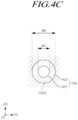
- FIGS. 4 A to 4 D are enlarged top views illustrating first to fourth through holes of FIG. 2
- FIGS. 5 A to 5 D are enlarged cross-sectional views illustrating the first to fourth through holes of FIG. 3 .
- the first through hole TH 1 may include a first portion A 11 , a second portion A 12 that is positioned on the first portion A 11 and communicates with the first portion A 11 , and a third portion A 13 that is positioned on the second portion A 12 and communicates with the second portion A 12 .
- the first portion A 11 , the second portion A 12 and the third portion A 13 may be centered on each other.
- the width of the first portion A 11 of the first through hole TH 1 may have a size of W 1
- the width of the second portion A 12 of the first through hole TH 1 may have a size of W 2 larger than W 1
- the width of the third portion A 13 of the first through hole TH 1 may have a size of W 3 larger than W 2 .
- the difference between W 3 and W 2 may be smaller than the difference between W 2 and W 1 .
- the first pad region PAD 1 of the electrode layer 20 corresponding to the first through hole TH 1 may be exposed, as illustrated in FIG. 5 A .
- the first pad region PAD 1 is positioned at the lower end of the second portion A 12 of the first through hole TH 1 , and when viewed from the top, may have a shape that surrounds the periphery of the first portion A 11 of the first through hole TH 1 .
- the second through hole TH 2 may include a first portion A 21 , a second portion A 22 that is positioned on the first portion A 21 and communicates with the first portion A 21 , and a third portion A 23 that is positioned on the second portion A 22 and communicates with the second portion A 22 .
- the width of the first portion A 21 of the second through hole TH 2 may have the same size as the width of the first portion A 11 of the first through hole TH 1
- the width of the second portion A 22 of the second through hole TH 2 may have the same size as the width of the third portion A 13 of the first through hole TH 1 .
- the width of the first portion A 11 of the first through hole TH 1 is W 1
- the width of the third portion A 13 of the first through hole TH 1 is W 3
- the width of the first portion A 21 of the second through hole TH 2 may be W 1
- the width of the second portion A 22 of the second through hole TH 2 may be W 3 .
- the thickness, as measured in the vertical direction VD, of the second portion A 22 of the second through hole TH 2 and the thickness of the third portion A 13 of the first through hole TH 1 may be the same as each other.
- the thickness of the second portion A 22 of the second through hole TH 2 and the thickness of the third portion A 13 of the first through hole TH 1 may have a size corresponding to four times the vertical pitch of the electrode layers 20 .
- the vertical pitch of the electrode layers 20 means the vertical distance between the top surfaces of the electrode layers 20 which are adjacent to each other in the vertical direction VD.
- the width of the third portion A 23 of the second through hole TH 2 may have a size of W 4 , which is greater than W 3 .
- the difference between W 4 and W 3 is smaller than the difference between W 3 and W 1 .
- the second pad region PAD 2 of the electrode layer 20 corresponding to the second through hole TH 2 may be exposed.
- the second pad region PAD 2 is positioned at the lower end of the second portion A 22 of the second through hole TH 2 , and when viewed from the top, may have a shape that surrounds the periphery of the first portion A 21 of the second through hole TH 2 .
- the third through hole TH 3 may include a first portion A 31 , and a second portion A 32 which is positioned on the first portion A 31 and communicates with the first portion A 31 .
- the width of the first portion A 31 of the third through hole TH 3 may have the same size as the width of the first portion A 11 of the first through hole TH 1 and the width of the first portion A 21 of the second through hole TH 2 .
- the width of the second portion A 32 of the third through hole TH 3 may have the same size as the width of the third portion A 23 of the second through hole TH 2 .
- the width of the first portion A 11 of the first through hole TH 1 and the width of the first portion A 21 of the second through hole TH 2 are W 1
- the width of the third portion A 23 of the second through hole TH 2 is W 4
- the width of the first portion A 31 of the third through hole TH 3 may be W 1
- the width of the second portion A 32 of the third through hole TH 3 may be W 4
- the thickness of the second portion A 32 of the third through hole TH 3 and the thickness of the third portion A 23 of the second through hole TH 2 may be the same.
- the thickness of the second portion A 32 of the third through hole TH 3 and the thickness of the third portion A 23 of the second through hole TH 2 may have a size corresponding to twelve (12) times the vertical pitch of the electrode layers 20 .
- the third pad region PAD 3 of the electrode layer 20 corresponding to the third through hole TH 3 may be exposed.
- the third pad region PAD 3 is positioned at the lower end of the second portion A 32 of the third through hole TH 3 , and when viewed from the top, may have a shape that surrounds the periphery of the first portion A 31 of the third through hole TH 3 .
- the fourth through hole TH 4 may include a first portion A 41 , and a second portion A 42 that is positioned on the first portion A 41 and communicates with the first portion A 41 .
- the width of the first portion A 41 of the fourth through hole TH 4 may be W 1
- the width of the second portion A 42 of the fourth through hole TH 4 may be W 2 . Due to the difference in size between the width W 2 of the second portion A 42 of the fourth through hole TH 4 and the width W 1 of the first portion A 41 of the fourth through hole TH 4 , the fourth pad region PAD 4 of the electrode layer 20 corresponding to the fourth through hole TH 4 may be exposed.
- the fourth pad region PAD 4 is positioned at the lower end of the second portion A 42 of the fourth through hole TH 4 , and when viewed from the top, may have a shape that surrounds the periphery of the first portion A 41 of the fourth through hole TH 4 .
- the first to fourth through holes TH 1 to TH 4 described above with reference to FIGS. 2 to 5 D may be formed by using a patterning method to be described below. That is to say, the first to fourth through holes TH 1 to TH 4 of FIGS. 2 to 5 D may be formed as a result of using the patterning method to be described below.
- FIG. 6 is a cross-sectional view after initial through holes of a three-dimensional memory device in accordance with an embodiment of the present disclosure are formed.
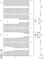
- FIGS. 7 A to 7 M are cross-sectional views illustrating process steps for forming through holes of a three-dimensional memory device in accordance with an embodiment of the present disclosure.
- FIGS. 8 A to 8 M are top views illustrating the process steps for forming the through holes of a three-dimensional memory device in accordance with an embodiment of the present disclosure.
- FIGS. 7 A to 8 M illustrate only one through hole for each of the first to fourth regions CNR 1 to CNR 4 .
- a stack ST may be formed by forming a lower thin film stack 100 on a first cell array region CAR 1 , a connection region CNR and a second cell array region CAR 2 of a substrate 10 and by stacking an upper thin film stack 200 on the lower thin film stack 100 .
- Each of the lower thin film stack 100 and the upper thin film stack 200 may include a plurality of first material layers 24 and a plurality of second material layers 22 , which are alternately stacked.
- the first material layers 24 and the second material layers 22 may be formed of different materials.
- the second material layers 22 may be formed of a dielectric material that may be used in interlayer dielectric layers, and the first material layers 24 may be formed of a dielectric material that may be used as sacrificial layers.
- the first material layers 24 have a different etch selectivity from the second material layers 22 .
- the first material layers 24 may be formed as silicon nitride layers
- the second material layers 22 may be formed as silicon oxide layers.
- Step structures STEP 1 to STEP 4 may be formed in first to fourth regions CNR 1 to CNR 4 , respectively, of the upper thin film stack 200 .
- a process for forming the step structures STEP 1 to STEP 4 may include steps of forming a mask pattern having openings that expose portions of the first to fourth regions CNR 1 to CNR 4 , respectively, on the upper thin film stack 200 ; etching the upper thin film stack 200 in a unit etching process using the mask pattern as an etch mask; performing a trimming process to reduce the area of the mask pattern; and alternately repeating the unit etching process and the trimming process.
- the etching thickness of the unit etching process may be substantially the same as the vertical pitch of the first material layers 24 .
- the vertical pitch of the first material layers 24 means the vertical distance between the top surfaces of the first material layers 24 that are adjacent to each other in the vertical direction VD.
- a plurality of step surfaces may be formed in each of the first to fourth regions CNR 1 to CNR 4 that correspond to the step structures STEP 1 to STEP 4 , respectively.
- Through holes TH may be formed to pass through the stack ST in the vertical direction VD.
- the through holes extend from the step surfaces of the step structures STEP 1 to STEP 4 through upper thin film stack 200 and lower thin film stack 100 to the substrate 10 .
- a process for forming the through holes TH may include a step of forming a mask pattern having openings that expose portions of the step surfaces, respectively, on the stack ST, and a step of etching the stack ST using the mask pattern as an etch mask.
- each through hole TH may extend to the substrate 10 by passing through the stack ST.
- each through hole TH may have a width of W 1 .
- Each through hole TH may include sidewalls formed of exposed portions of the alternating layers in the stack ST
- a first mask PR 1 may be formed to fill the through holes TH and cover the stack ST, and a first opening OP 1 , which passes through the first mask PR 1 , may be formed to align with the center portion of the through hole TH of the first region CNR 1 by a patterning process.
- the through hole TH of the first region CNR 1 which has the width of W 1 , may be used as an overlay key.
- a first isotropic etching process may be performed on the first mask PR 1 .
- the first isotropic etching process may reduce the area and thickness of the first mask PR 1 .
- the first mask PR 1 in the through hole TH of the first region CNR 1 is etched to expose the portions of the stack ST common to the sidewalls of the previously formed through hole TH of FIG. 7 A .
- the first opening OP 1 in the remaining first mask PR 1 which is disposed over stack ST in first region CNR 1 , is expanded or widened horizontally in directions parallel to the first direction FD and the second direction SD.
- the first opening OP 1 may be expanded or widened horizontally relative to the through hole TH of the first region CNR 1 .
- the width of the first opening OP 1 may be larger than the width of the through hole TH.
- the width of the through hole TH may have the size of W 1
- the width of the expanded first opening OP 1 may have a size of W 2 , which is greater than W 1 .
- a first recess etching process of etching the stack ST using the isotropically etched first mask PR 1 as an etch mask may be performed.
- the etching thickness of the first recess etching process may have a size corresponding to K (where K is a natural number equal to or greater than two) times the vertical pitch of the first material layers 24 .
- FIG. 7 D illustrates an example in which K is four.
- the width of the upper portion of the through hole TH of the first region CNR 1 is increased.
- the width of the upper portion of the through hole TH of the first region CNR 1 may be W 2 , which is larger than W 1 .
- the difference in size between the width W 2 of the upper portion and the width W 1 of the lower portion of the through hole TH of the first region CNR 1 may correspond to the difference in size between the width of the second portion A 12 and the width of the first portion A 11 of the first through hole TH 1 described above with reference to FIGS. 4 A and 5 A .
- the first mask PR 1 may be formed as a photoresist.
- the first mask PR 1 that remains after the first recess etching process may be removed through a strip process.
- a second mask PR 2 may be formed to fill the through holes TH and cover the stack ST.
- Second openings OP 2 which pass through the second mask PR 2 in the vertical direction VD, may be formed by a patterning process in the center portion of the through hole TH of the first region CNR 1 and in the center portion of the through hole TH of the second region CNR 2 .
- the center of a second opening OP 2 may align with the center of a corresponding through hole TH.
- the lower portion of the through hole TH of the first region CNR 1 , which has the width of W 1 , and the through hole TH of the second region CNR 2 , which has the width of W 1 may be used as an overlay key.
- a second isotropic etching process may be performed on the second mask PR 2 .
- the area and thickness of the second mask PR 2 may be reduced in the second isotropic etching process.
- Portions of stack ST in the first region CNR 1 that were previously exposed in the sidewalls of through hole TH of FIGS. 7 A and 7 D , and portions of stack ST in the second region CNR 2 that were previously exposed in the sidewalls of through hole TH of FIG. 7 A may be exposed again with the removal of the second mask PR 2 .
- the second openings OP 2 are expanded or widened horizontally.
- the size of the second openings OP 2 may be expanded or widened, with the size adjusted depending on the size and location of the through holes TH of the first region CNR 1 and the second region CNR 2 such that a difference between the size of the second opening OP 2 and the size of the through hole TH in the first region CNR 1 become first preset value and a difference between the size of the second opening OP 2 and the size of the through hole TH in the second region CNR 2 become a second preset value.
- the width of the second openings OP 2 may have a size larger than the width of the through holes TH of both the first region CNR 1 and the second region CNR 2 .
- the width of the through hole TH may have the size of W 1
- the width of the expanded second opening OP 2 may have a size of W 3 , which is larger than W 1
- W 3 may be slightly larger than W 2 , which is the width of the upper portion of the through hole TH of the first region CNR 1 .
- a second recess etching process may be performed to etch the stack ST using the isotropically etched second mask PR 2 as an etch mask.
- the etching thickness of the second recess etching process may have a size corresponding to M (where M is a natural number equal to or greater than two) times the vertical pitch of the first material layers 24 .
- FIG. 7 G illustrates an example in which M is four.
- the second recess etching process therefore extends, in a vertical direction VD, the width W 2 of the upper portion of the through hole TH of the first region CNR 1 (illustrated in FIG. 7 F ).
- the thickness of the stack ST including the lower portion of through hole TH in first region CNR 1 which has a width W 1 , is reduced by the etching thickness of the second recess etching process.
- the second recess etching process may be used to increase the width of the upper portion of the through hole TH of the first region CNR 1 and the width of the upper portion of the through hole TH of the second region CNR 2 .
- the width of the upper portion of the through hole TH of the first region CNR 1 and the width of the upper portion of the through hole TH of the second region CNR 2 may be etched to W 3 through the etching thickness of the second recess etching process.
- W 3 may be larger than W 2 .
- the difference in size between the width W 3 of the upper portion and the width W 1 of the lower portion of the through hole TH of the second region CNR 2 may correspond to the difference in size between the width of the second portion A 22 and the width of the first portion A 21 of the second through hole TH 2 described above with reference to FIGS. 4 B and 5 B .
- the second mask PR 2 may be formed as a photoresist.
- the second mask PR 2 remaining after the second recess etching process may be removed through a strip process.
- a third mask PR 3 may be formed to fill the through holes TH and cover the stack ST.
- Third openings OP 3 that vertically pass through the third mask PR 3 may be formed at the center portion of the through hole TH of the second region CNR 2 and the center portion of the through hole TH of the third region CNR 3 by a patterning process.
- the center of a third opening OP 3 may align with the center of a corresponding through hole TH.
- No third opening OP 3 is formed in the first region CNR 1 or the fourth region CNR 4 .
- the lower portion of the through hole TH of the second region CNR 2 , which has the width of W 1 , and the through hole TH of the third region CNR 3 , which has the width of W 1 may be used as an overlay key.
- a third isotropic etching process may be performed on the third mask PR 3 .
- the area and thickness of the third mask PR 3 may be reduced. Portions of stack ST in the second region CNR 2 and in the third region CNR 3 that, in earlier processes (see FIGS. 7 G and 7 A ), were previously exposed in the sidewalls of the respective through holes TH may be exposed again with the removal of the third mask PR 3 .
- the third openings OP 3 are expanded or widened horizontally.
- the size of the third openings OP 3 may be expanded or widened, with the size adjusted depending on the size and location of the through holes TH of the second region CNR 2 and the third region CNR 3 , such that a difference between the size of the third opening OP 3 and the size of the through hole TH in the second region CNR 2 become third preset value and a difference between the size of the third opening OP 3 and the size of the through hole TH in the third region CNR 3 become a fourth preset value.
- the width of the third openings OP 3 may have a size larger than the width of the through hole TH of both the second region CNR 2 and the third region CNR 3 .
- the width of the through hole TH of the third region CNR 3 may have the size of W 1
- the width of the expanded third opening OP 3 may have a size of W 4 , which is larger than W 1
- W 4 may be slightly larger than W 3 , which is the width of the upper portion of the through hole TH of the second region CNR 2 .
- a third recess etching process may be performed to etch the stack ST using the isotropically etched third mask PR 3 as an etch mask.
- the etching thickness of the third recess etching process may have a size corresponding to N (where N is a natural number equal to or greater than two) times the vertical pitch of the first material layers 24 .
- FIG. 7 J illustrates a case where N is twelve.
- the third recess etching process therefore extends, in a vertical direction VD, the width W 3 of the upper portion of the through hole TH of the second region CNR 2 (illustrated in FIG. 7 I ).
- the thickness of the stack ST including the lower portion of through hole TH, which has a width W 1 is reduced by the etching thickness of the third recess etching process.
- the third recess etching process may also be used to increase the width of the upper portion of the through hole TH of the second region CNR 2 and the width of the upper portion of the through hole TH of the third region CNR 3 .
- the width of the upper portion of the through hole TH of the second region CNR 2 and the width of the upper portion of the through hole TH of the third region CNR 3 may etched to through the etching thickness of the third recess etching process.
- W 4 may be larger than W 3 .
- the difference in size between the width W 4 of the upper portion and the width W 1 of the lower portion of the through hole TH of the third region CNR 3 may correspond to the difference in size between the width of the second portion A 32 and the width of the first portion A 31 of the third through hole TH 3 described above with reference to FIGS. 4 C and 5 C .
- the third mask PR 3 may be formed as a photoresist.
- the third mask PR 3 that remains after the third recess etching process may be removed through a strip process.
- a fourth mask PR 4 may be formed to fill the through holes TH and to cover the stack ST.
- a fourth opening OP 4 which passes vertically through the fourth mask PR 4 , may be formed at the center portion of the through hole TH of the fourth region CNR 4 by a patterning process.
- the through hole TH of the fourth region CNR 4 which has the width of W 1 , may be used as an overlay key.
- the center of a fourth opening OP 4 may align with the center of a corresponding through hole TH. No fourth openings OP 4 are formed in the first through third regions CNR 1 to CNR 3 .
- a fourth isotropic etching process may be performed on the fourth mask PR 4 .
- the fourth isotropic etching process may reduce the area and thickness of the fourth mask PR 4 in the through hole TH of the fourth region CNR 4 is etched to expose the portions of the stack ST common to the sidewalls of the previously formed through hole TH of FIG. 7 A .
- the fourth opening OP 4 in the remaining first mask PR 4 which is disposed over stack ST in fourth region CNR 4 , is expanded or widened horizontally in directions parallel to the first direction FD and the second direction SD.
- the fourth opening OP 4 may be expanded or widened horizontally relative to the through hole TH of the fourth region CNR 4 .
- the width of the through hole TH of the fourth region CNR 4 may have the size of W 1
- the width of the expanded fourth opening OP 4 may have the size of W 2 larger than W 1 .
- a fourth recess etching process of etching the stack ST using the isotropically etched fourth mask PR 4 as an etch mask may be performed.
- the etching thickness of the fourth recess etching process may have a size corresponding to R (where R is a natural number equal to or greater than two) times the vertical pitch of the first material layers 24 .
- FIG. 7 M illustrates an example in which R is four.
- the width of the upper portion of the through hole TH of the fourth region CNR 4 is increased.
- the width of the lower portion of the through hole TH of the fourth region CNR 4 may be W 1
- the width of the upper portion of the through hole TH of the fourth region CNR 4 may be W 2 .
- the difference in size between the width W 2 of the upper portion and the width W 1 of the lower portion of the through hole TH of the fourth region CNR 4 may correspond to the difference in size between the width of the second portion A 42 and the width of the first portion A 41 of the fourth through hole TH 4 described above with reference to FIGS. 4 D and 5 D .
- the fourth mask PR 4 may be formed as a photoresist.
- the fourth mask PR 4 remaining after the fourth recess etching process may be removed through a strip process.
- electrode layers may be formed by replacing the first material layers 24 with a conductive material.
- FIGS. 9 A to 9 F are cross-sectional views illustrating process steps for manufacturing a three-dimensional memory device in a comparative example
- FIG. 10 is a top view illustrating through holes of the three-dimensional memory in a comparative example.
- a stack ST may be formed by stacking a lower thin film stack 100 and an upper thin film stack 200 on a substrate 10 , and step structures may be formed in first to fourth regions CNR 1 to CNR 4 , respectively, of the upper thin film stack 200 .
- a first mask PR 11 is formed on the stack ST, which is formed with step structures.
- First openings OP 11 are formed in the first mask PR 11 .
- the first openings OP 11 expose step surfaces, respectively, of the step structure of the first region CNR 1 .
- First holes H 1 are formed by etching portions of the stack ST that are exposed by the first openings OP 11 through a first recess etching process that uses the first mask PR 11 as an etch mask.
- a second mask PR 12 is formed on the stack ST.
- Second openings OP 12 are formed in the second mask PR 12 .
- the second openings OP 12 expose the first holes H 1 of the first region CNR 1 and stepped surfaces of the step structure of the second region CNR 2 , respectively.
- the second opening OP 12 should be formed to have a width larger by at least a predetermined size than the first hole H 1 .
- the width of the second opening OP 12 should have a size of W 12 , which is larger by at least a predetermined size than W 11 .
- portions of the stack ST that are exposed by the second openings OP 12 are etched by a second recess etching process using the second mask PR 12 as an etch mask.
- the depth of the first holes H 1 of the first region CNR 1 is increased, and second holes H 2 are formed in the second region CNR 2 .
- a third mask PR 13 is formed on the stack ST.
- Third openings OP 13 that expose the second holes H 2 of the second region CNR 2 and stepped surfaces of the step structure of the third region CNR 3 , respectively, are formed in the third mask PR 13 .
- the third opening OP 13 should be formed to have a width larger by at least a predetermined size than the second hole H 2 .
- the width of the third opening OP 13 should have a size of W 13 , which is larger by at least a predetermined size than W 12 .
- portions of the stack ST that are exposed by the third openings OP 13 are etched by a third recess etching process using the third mask PR 13 as an etch mask.
- the third recess etching process the depth of the second holes H 2 of the second region CNR 2 is increased, and third holes H 3 are formed in the third region CNR 3 .
- a fourth mask PR 14 is formed on the stack ST, and fourth openings OP 14 are formed in the fourth mask PR 14 that expose step surfaces of the step structure of the fourth region CNR 4 .
- Fourth holes H 4 are formed by etching portions of the stack ST that are exposed by the fourth openings OP 14 , through a fourth recess etching process that uses the fourth mask PR 14 as an etch mask.
- electrode layers may be formed by replacing first material layers 24 with a conductive material.
- pad regions of the electrode layers are positioned at the bottom surfaces of the first to fourth holes H 1 to H 4 .
- the second opening OP 12 of the second mask PR 12 should be formed to have a width larger by at least a predetermined size than the first hole H 1
- the third opening OP 13 of the third mask PR 13 should be formed to have a width larger by at least a predetermined size than the second hole H 2 .
- the width of the opening should be larger by at least a predetermined size than the width of an underlying hole in order for the overlay with the underlying hole.
- the width of an opening is increased by at least a predetermined size each time a recess etching process is performed.
- the widths of the holes continue to increase incrementally from each recess etching process. Accordingly, as the width of the hole becomes excessively large, failures may occur. For example, as illustrated in FIG. 10 , the electrode layers of an electrode structure ES are disconnected by the presence of the holes H 2 and H 3 .
- FIG. 11 is a block diagram a three-dimensional memory device in accordance with an embodiment of the present disclosure.
- a memory device in accordance with an embodiment of the disclosure may include a memory cell array 300 and a logic circuit 400 .
- the logic circuit 400 may include a row decoder (X-DEC) 410 , a page buffer circuit 420 and a peripheral circuit (PERI circuit) 430 .
- X-DEC row decoder
- PROI circuit peripheral circuit
- the memory cell array 300 may be coupled to the row decoder (X-DEC) 410 through a plurality of row lines RL.
- the row lines RL may include at least one drain select line, a plurality of word lines and at least one source select line.
- the memory cell array 300 may be coupled to the page buffer circuit 420 through bit lines BL.
- the memory cell array 300 may include a plurality of memory blocks BLK.
- a memory block BLK may include a plurality of pages.
- the memory block BLK may be a basic unit of an erase operation, and the page may be a basic unit of a read operation.
- memory cell array 300 may include a plurality of memory cells that are disposed in regions where the plurality of bit lines BL and the plurality of word lines WL intersect.
- the memory cell may be a volatile memory cell that loses data stored therein when power supply is cut off, or may be a nonvolatile memory cell that retains data stored therein even when power supply is cut off.
- the memory device may be a DRAM (dynamic random access memory), an SRAM (static random access memory), a mobile DRAM, a DDR SDRAM (double data rate synchronous dynamic random access memory), an LPDDR (low power DDR) SDRAM, a GDDR (graphic DDR) SDRAM or an RDRAM (Rambus dynamic random access memory).
- DRAM dynamic random access memory
- SRAM static random access memory
- mobile DRAM a DDR SDRAM (double data rate synchronous dynamic random access memory)
- LPDDR (low power DDR) SDRAM a GDDR (graphic DDR) SDRAM or an RDRAM (Rambus dynamic random access memory).
- LPDDR low power DDR SDRAM
- GDDR graphics DDR SDRAM
- RDRAM Rabus dynamic random access memory
- the memory device may be an EEPROM (electrically erasable programmable read-only memory), a flash memory, a PRAM (phase change random access memory), an RRAM (resistive random access memory), an NFGM (nano-floating gate memory), a PoRAM (polymer random access memory), an MRAM (magnetic random access memory) or an FRAM (ferroelectric random access memory).
- the memory device may be a hybrid memory that includes both volatile memory cells and nonvolatile memory cells.
- the memory cell may be a single level cell (SLC) that stores one-bit data or a multi-level cell (MLC) that stores two or more-bit data.
- the multi-level cell may store two-bit data, three-bit data, four-bit data, and so forth.
- the cell region 110 may include at least one of single level cells and multi-level cells.
- the row decoder (X-DEC) 410 may select any one from among the memory blocks BLK included in the memory cell array 300 , in response to a row address X_A provided from the peripheral circuit (PERI circuit) 430 .
- the row decoder (X-DEC) 410 may transfer an operating voltage X_V, provided from the peripheral circuit (PERI circuit) 430 , to row lines RL coupled to a memory block BLK selected from among the memory blocks BLK included in the memory cell array 300 .
- the page buffer circuit 420 may include a plurality of page buffers PB, which are coupled to the bit lines BL, respectively.
- the page buffer circuit 420 may receive a page buffer control signal PB_C from the peripheral circuit (PERI circuit) 430 , and may transmit and receive a data signal DATA to and from the peripheral circuit (PERI circuit) 430 .
- the page buffer circuit 420 may control the bit lines BL, which are arranged in the memory cell array 300 , in response to the page buffer control signal PB_C.
- the page buffer circuit 420 may detect data, stored in a memory cell of the memory cell array 300 , by sensing the signal of a bit line BL of the memory cell array 300 in response to the page buffer control signal PB_C, and may transmit the data signal DATA to the peripheral circuit (PERI circuit) 430 depending on the detected data.
- the peripheral circuit PERI circuit
- the page buffer circuit 420 may apply a signal to the bit line BL based on the data signal DATA, received from the peripheral circuit (PERI circuit) 430 , in response to the page buffer control signal PB_C, and thereby, may write data to the memory cell of the memory cell array 300 .
- the page buffer circuit 420 may write data to or read data from memory cells, which are coupled to an activated word line.
- the peripheral circuit (PERI circuit) 430 may receive a command signal CMD, an address signal ADD and a control signal CTRL from outside the memory device, and may transmit and receive data DATA to and from a device outside the memory device, for example, a memory controller.
- the peripheral circuit (PERI circuit) 430 may output signals for writing data to the memory cell array 300 or reading data from the memory cell array 300 , for example, the row address X_A, the page buffer control signal PB_C and so forth, based on the command signal CMD, the address signal ADD and the control signal CTRL.
- the peripheral circuit (PERI circuit) 430 may generate various voltages including the operating voltage X_V, which are required in the memory device.
- the memory cell array 300 and the logic circuit 400 may be vertically overlapped with each other.
- the memory device according to the present embodiment may be provided in a Peri Under Cell (PUC) structure or a Peri Over Cell (POC) structure.
- PUC Peri Under Cell
- POC Peri Over Cell
- FIG. 12 is a block diagram schematically illustrating a memory system including a three-dimensional memory device in accordance with an embodiment of the present disclosure.
- a memory system 500 may store data to be accessed by a host 600 such as a mobile phone, an MP3 player, a laptop computer, a desktop computer, a game player, a TV, an in-vehicle infotainment system, and so forth.
- a host 600 such as a mobile phone, an MP3 player, a laptop computer, a desktop computer, a game player, a TV, an in-vehicle infotainment system, and so forth.
- the memory system 500 may be manufactured as any one of various kinds of storage devices according to the protocol of an interface that is electrically coupled to the host 600 .
- the memory system 500 may be configured as any one of various kinds of storage devices such as a solid state drive, a multimedia card in the form of an MMC, an eMMC, an RS-MMC and a micro-MMC, a secure digital card in the form of an SD, a mini-SD and a micro-SD, a universal serial bus (USB) storage device, a universal flash storage (UFS) device, a Personal Computer Memory Card International Association (PCMCIA) card type storage device, a peripheral component interconnection (PCI) card type storage device, a PCI express (PCI-E) card type storage device, a compact flash (CF) card, a smart media card, a memory stick, and so forth.
- a solid state drive such as a solid state drive, a multimedia card in the form of an MMC, an eMMC, an RS-MMC and a
- the memory system 500 may be manufactured as any one among various kinds of package types.
- the memory system 500 may be manufactured as any one of various kinds of package types such as a package-on-package (POP), a system-in-package (SIP), a system-on-chip (SOC), a multi-chip package (MCP), a chip-on-board (COB), a wafer-level fabricated package (WFP) and a wafer-level stack package (WSP).
- POP package-on-package
- SIP system-in-package
- SOC system-on-chip
- MCP multi-chip package
- COB chip-on-board
- WFP wafer-level fabricated package
- WSP wafer-level stack package
- the memory system 500 may include a nonvolatile memory device 510 and a controller 520 .
- the nonvolatile memory device 510 may operate as a storage medium of the memory system 500 .
- the nonvolatile memory device 510 may be configured by any one of various types of nonvolatile memory devices such as a NAND flash memory device, a NOR flash memory device, a ferroelectric random access memory (FRAM) using a ferroelectric capacitor, a magnetic random access memory (MRAM) using a tunneling magneto-resistive (TMR) layer, a phase change random access memory (PRAM) using a chalcogenide alloy, and a resistive random access memory (RERAM) using a transition metal compound, depending on memory cells.
- a NAND flash memory device a NOR flash memory device
- FRAM ferroelectric random access memory
- MRAM magnetic random access memory
- TMR tunneling magneto-resistive
- PRAM phase change random access memory
- RERAM resistive random access memory
- FIG. 12 illustrates that the memory system 500 includes one nonvolatile memory device 510 , this is only for the sake of convenience in explanation, and the memory system 500 may include a plurality of nonvolatile memory devices.
- the present disclosure may be applied the same to the memory system 500 including a plurality of nonvolatile memory devices.
- the nonvolatile memory device 510 may include memory devices according to the embodiments of the present disclosure.
- the controller 520 may control general operations of the memory system 500 through driving of firmware or software loaded in a memory 523 .
- the controller 520 may decode and drive a code type instruction or algorithm such as firmware or software.
- the controller 520 may be implemented in the form of hardware or in a combined form of hardware and software.
- the controller 520 may include a host interface 521 , a processor 522 , the memory 523 and a memory interface 524 . Although not illustrated in FIG. 12 , the controller 520 may further include an ECC (error correction code) engine that generates a parity by ECC-encoding write data provided from the host 600 and ECC-decodes read data, read from the nonvolatile memory device 510 , by using the parity.
- ECC error correction code
- the host interface 521 may interface the host 600 and the memory system 500 in correspondence to the protocol of the host 600 .
- the host interface 521 may communicate with the host 600 through any one of universal serial bus (USB), universal flash storage (UFS), multimedia card (MMC), parallel advanced technology attachment (PATA), serial advanced technology attachment (SATA), small computer system interface (SCSI), serial attached SCSI (SAS), peripheral component interconnection (PCI) and PCI express (PCI-E) protocols.
- USB universal serial bus
- UFS universal flash storage
- MMC multimedia card
- PATA parallel advanced technology attachment
- SATA serial advanced technology attachment
- SATA small computer system interface
- SAS serial attached SCSI
- PCI-E PCI express
- the processor 522 may be configured by a micro control unit (MCU) or a central processing unit (CPU).
- the processor 522 may process a request transmitted from the host 600 .
- the processor 522 may drive a code type instruction or algorithm, that is, firmware, loaded in the memory 523 , and may control the internal function blocks such as the host interface 521 , the memory 523 and the memory interface 524 and the nonvolatile memory device 510 .
- the processor 522 may generate control signals for controlling the operation of the nonvolatile memory device 510 , on the basis of requests transmitted from the host 600 , and may provide the generated control signals to the nonvolatile memory device 510 through the memory interface 524 .
- the memory 523 may be configured by a random access memory such as a dynamic random access memory (DRAM) or a static random access memory (SRAM).
- the memory 523 may store firmware to be driven by the processor 522 .
- the memory 523 may store data necessary for driving the firmware, for example, metadata. Namely, the memory 523 may operate as a working memory of the processor 522 .
- the memory 523 may be configured to include a data buffer for temporarily storing write data to be transmitted from the host 600 to the nonvolatile memory device 510 or read data to be transmitted from the nonvolatile memory device 510 to the host 600 . In other words, the memory 523 may operate as a buffer memory. The memory 523 may receive and store map data from the nonvolatile memory device 510 when the memory system 500 is booted.
- the memory interface 524 may control the nonvolatile memory device 510 under the control of the processor 522 .
- the memory interface 524 may also be referred to as a memory controller.
- the memory interface 524 may provide control signals to the nonvolatile memory device 510 .
- the control signals may include a command, an address, an operation control signal and so forth for controlling the nonvolatile memory device 510 .
- the memory interface 524 may provide data, stored in the data buffer, to the nonvolatile memory device 510 , or may store data, transmitted from the nonvolatile memory device 510 , in the data buffer.
- the controller 520 may further include a map cache (not illustrated) that caches map data referred to by the processor 522 among map data stored in the memory 523 .
- a map cache (not illustrated) that caches map data referred to by the processor 522 among map data stored in the memory 523 .
- FIG. 13 is a block diagram schematically illustrating a computing system including a three-dimensional memory device in accordance with embodiments of the disclosure.
- a computing system 700 in accordance with an embodiment may include a memory system 710 , a microprocessor (CPU) 720 , a RAM 730 , a user interface 740 and a modem 750 such as a baseband chipset, which are electrically coupled to a system bus 760 .
- a battery (not shown) for supplying the operating voltage of the computing system 700 may be additionally provided.
- the computing system 700 in accordance with the embodiment may be additionally provided with an application chipset, a camera image processor (CIS), a mobile DRAM, and so on.
- the memory system 710 may configure, for example, an SSD (solid state drive/disk) that uses a nonvolatile memory to store data. Otherwise, the memory system 710 may be provided as a fusion flash memory (for example, a OneNAND flash memory).
Landscapes
- Semiconductor Memories (AREA)
Abstract
Description
Claims (11)
Applications Claiming Priority (2)
| Application Number | Priority Date | Filing Date | Title |
|---|---|---|---|
| KR1020210142597A KR20230058868A (en) | 2021-10-25 | 2021-10-25 | Three dimensional memory device and method for fabricating the same |
| KR10-2021-0142597 | 2021-10-25 |
Publications (2)
| Publication Number | Publication Date |
|---|---|
| US20230129701A1 US20230129701A1 (en) | 2023-04-27 |
| US12302567B2 true US12302567B2 (en) | 2025-05-13 |
Family
ID=86056857
Family Applications (1)
| Application Number | Title | Priority Date | Filing Date |
|---|---|---|---|
| US17/703,893 Active 2043-09-10 US12302567B2 (en) | 2021-10-25 | 2022-03-24 | Three-dimensional memory device and manufacturing method thereof |
Country Status (2)
| Country | Link |
|---|---|
| US (1) | US12302567B2 (en) |
| KR (1) | KR20230058868A (en) |
Citations (4)
| Publication number | Priority date | Publication date | Assignee | Title |
|---|---|---|---|---|
| KR20120035399A (en) | 2010-10-05 | 2012-04-16 | 에스케이하이닉스 주식회사 | Method for forming the semiconductor device |
| KR20180110797A (en) | 2017-03-30 | 2018-10-11 | 에스케이하이닉스 주식회사 | Semiconductor device and manufacturing method thereof |
| US20200295028A1 (en) * | 2019-03-15 | 2020-09-17 | SK Hynix Inc. | Vertical semiconductor device and fabrication method thereof |
| US10930587B2 (en) | 2019-01-16 | 2021-02-23 | SK Hynix Inc. | Semiconductor memory device |
-
2021
- 2021-10-25 KR KR1020210142597A patent/KR20230058868A/en not_active Withdrawn
-
2022
- 2022-03-24 US US17/703,893 patent/US12302567B2/en active Active
Patent Citations (4)
| Publication number | Priority date | Publication date | Assignee | Title |
|---|---|---|---|---|
| KR20120035399A (en) | 2010-10-05 | 2012-04-16 | 에스케이하이닉스 주식회사 | Method for forming the semiconductor device |
| KR20180110797A (en) | 2017-03-30 | 2018-10-11 | 에스케이하이닉스 주식회사 | Semiconductor device and manufacturing method thereof |
| US10930587B2 (en) | 2019-01-16 | 2021-02-23 | SK Hynix Inc. | Semiconductor memory device |
| US20200295028A1 (en) * | 2019-03-15 | 2020-09-17 | SK Hynix Inc. | Vertical semiconductor device and fabrication method thereof |
Also Published As
| Publication number | Publication date |
|---|---|
| US20230129701A1 (en) | 2023-04-27 |
| KR20230058868A (en) | 2023-05-03 |
Similar Documents
| Publication | Publication Date | Title |
|---|---|---|
| US10643704B2 (en) | Semiconductor memory device | |
| US10971487B2 (en) | Semiconductor memory device | |
| US10923495B2 (en) | Semiconductor memory device with divided source plate | |
| US11569265B2 (en) | Three-dimensional memory device and manufacturing method thereof | |
| KR102944848B1 (en) | 3D memory device and method for forming the same | |
| US11961552B2 (en) | Memory device including partial pages in memory blocks | |
| US11342353B2 (en) | Semiconductor memory device having three-dimensional structure and method for manufacturing the same | |
| US12417989B2 (en) | Semiconductor memory device including stacked semiconductor layers | |
| US12424545B2 (en) | Three-dimensional memory device | |
| US12376306B2 (en) | Semiconductor device including pass transistors | |
| US12302567B2 (en) | Three-dimensional memory device and manufacturing method thereof | |
| US20230343705A1 (en) | Three-dimensional memory device and manufacturing method thereof | |
| US20230168707A1 (en) | Memory controller for a memory device | |
| US20230207013A1 (en) | Memory device including row decoder | |
| US12317516B2 (en) | Semiconductor device including capacitors and manufacturing method thereof | |
| US12376305B2 (en) | Memory device and manufacturing method thereof | |
| US11776585B2 (en) | Memory device including a pass transistor circuit and a discharge transistor circuit | |
| KR102916269B1 (en) | Memory device having pass transistor circuit | |
| KR102897622B1 (en) | Three dimensional memory device | |
| US12302568B2 (en) | Semiconductor memory device including a discharge contact | |
| US10854294B1 (en) | Semiconductor memory device having pass transistors | |
| KR20230016829A (en) | Three dimensional memory device and method for fabricating the same | |
| KR20220170041A (en) | Memory device having block select circuit |
Legal Events
| Date | Code | Title | Description |
|---|---|---|---|
| AS | Assignment |
Owner name: SK HYNIX INC., KOREA, REPUBLIC OF Free format text: ASSIGNMENT OF ASSIGNORS INTEREST;ASSIGNORS:OH, SUNG LAE;SUNG, SANG HYUN;SHIN, HYUN SOO;REEL/FRAME:059396/0078 Effective date: 20220323 |
|
| FEPP | Fee payment procedure |
Free format text: ENTITY STATUS SET TO UNDISCOUNTED (ORIGINAL EVENT CODE: BIG.); ENTITY STATUS OF PATENT OWNER: LARGE ENTITY |
|
| STPP | Information on status: patent application and granting procedure in general |
Free format text: DOCKETED NEW CASE - READY FOR EXAMINATION |
|
| STPP | Information on status: patent application and granting procedure in general |
Free format text: NON FINAL ACTION MAILED |
|
| STPP | Information on status: patent application and granting procedure in general |
Free format text: RESPONSE TO NON-FINAL OFFICE ACTION ENTERED AND FORWARDED TO EXAMINER |
|
| STPP | Information on status: patent application and granting procedure in general |
Free format text: NOTICE OF ALLOWANCE MAILED -- APPLICATION RECEIVED IN OFFICE OF PUBLICATIONS |
|
| STCF | Information on status: patent grant |
Free format text: PATENTED CASE |