US12295173B2 - Display substrate including first and second node control circuitries and display device - Google Patents
Display substrate including first and second node control circuitries and display device Download PDFInfo
- Publication number
- US12295173B2 US12295173B2 US18/022,884 US202218022884A US12295173B2 US 12295173 B2 US12295173 B2 US 12295173B2 US 202218022884 A US202218022884 A US 202218022884A US 12295173 B2 US12295173 B2 US 12295173B2
- Authority
- US
- United States
- Prior art keywords
- transistor
- electrode
- node
- electrically coupled
- gate electrode
- Prior art date
- Legal status (The legal status is an assumption and is not a legal conclusion. Google has not performed a legal analysis and makes no representation as to the accuracy of the status listed.)
- Active
Links
Images


Classifications
-
- G—PHYSICS
- G09—EDUCATION; CRYPTOGRAPHY; DISPLAY; ADVERTISING; SEALS
- G09G—ARRANGEMENTS OR CIRCUITS FOR CONTROL OF INDICATING DEVICES USING STATIC MEANS TO PRESENT VARIABLE INFORMATION
- G09G3/00—Control arrangements or circuits, of interest only in connection with visual indicators other than cathode-ray tubes
- G09G3/20—Control arrangements or circuits, of interest only in connection with visual indicators other than cathode-ray tubes for presentation of an assembly of a number of characters, e.g. a page, by composing the assembly by combination of individual elements arranged in a matrix no fixed position being assigned to or needed to be assigned to the individual characters or partial characters
- G09G3/22—Control arrangements or circuits, of interest only in connection with visual indicators other than cathode-ray tubes for presentation of an assembly of a number of characters, e.g. a page, by composing the assembly by combination of individual elements arranged in a matrix no fixed position being assigned to or needed to be assigned to the individual characters or partial characters using controlled light sources
- G09G3/30—Control arrangements or circuits, of interest only in connection with visual indicators other than cathode-ray tubes for presentation of an assembly of a number of characters, e.g. a page, by composing the assembly by combination of individual elements arranged in a matrix no fixed position being assigned to or needed to be assigned to the individual characters or partial characters using controlled light sources using electroluminescent panels
- G09G3/32—Control arrangements or circuits, of interest only in connection with visual indicators other than cathode-ray tubes for presentation of an assembly of a number of characters, e.g. a page, by composing the assembly by combination of individual elements arranged in a matrix no fixed position being assigned to or needed to be assigned to the individual characters or partial characters using controlled light sources using electroluminescent panels semiconductive, e.g. using light-emitting diodes [LED]
- G09G3/3208—Control arrangements or circuits, of interest only in connection with visual indicators other than cathode-ray tubes for presentation of an assembly of a number of characters, e.g. a page, by composing the assembly by combination of individual elements arranged in a matrix no fixed position being assigned to or needed to be assigned to the individual characters or partial characters using controlled light sources using electroluminescent panels semiconductive, e.g. using light-emitting diodes [LED] organic, e.g. using organic light-emitting diodes [OLED]
- G09G3/3225—Control arrangements or circuits, of interest only in connection with visual indicators other than cathode-ray tubes for presentation of an assembly of a number of characters, e.g. a page, by composing the assembly by combination of individual elements arranged in a matrix no fixed position being assigned to or needed to be assigned to the individual characters or partial characters using controlled light sources using electroluminescent panels semiconductive, e.g. using light-emitting diodes [LED] organic, e.g. using organic light-emitting diodes [OLED] using an active matrix
-
- G—PHYSICS
- G09—EDUCATION; CRYPTOGRAPHY; DISPLAY; ADVERTISING; SEALS
- G09G—ARRANGEMENTS OR CIRCUITS FOR CONTROL OF INDICATING DEVICES USING STATIC MEANS TO PRESENT VARIABLE INFORMATION
- G09G3/00—Control arrangements or circuits, of interest only in connection with visual indicators other than cathode-ray tubes
- G09G3/20—Control arrangements or circuits, of interest only in connection with visual indicators other than cathode-ray tubes for presentation of an assembly of a number of characters, e.g. a page, by composing the assembly by combination of individual elements arranged in a matrix no fixed position being assigned to or needed to be assigned to the individual characters or partial characters
- G09G3/22—Control arrangements or circuits, of interest only in connection with visual indicators other than cathode-ray tubes for presentation of an assembly of a number of characters, e.g. a page, by composing the assembly by combination of individual elements arranged in a matrix no fixed position being assigned to or needed to be assigned to the individual characters or partial characters using controlled light sources
- G09G3/30—Control arrangements or circuits, of interest only in connection with visual indicators other than cathode-ray tubes for presentation of an assembly of a number of characters, e.g. a page, by composing the assembly by combination of individual elements arranged in a matrix no fixed position being assigned to or needed to be assigned to the individual characters or partial characters using controlled light sources using electroluminescent panels
- G09G3/32—Control arrangements or circuits, of interest only in connection with visual indicators other than cathode-ray tubes for presentation of an assembly of a number of characters, e.g. a page, by composing the assembly by combination of individual elements arranged in a matrix no fixed position being assigned to or needed to be assigned to the individual characters or partial characters using controlled light sources using electroluminescent panels semiconductive, e.g. using light-emitting diodes [LED]
- G09G3/3208—Control arrangements or circuits, of interest only in connection with visual indicators other than cathode-ray tubes for presentation of an assembly of a number of characters, e.g. a page, by composing the assembly by combination of individual elements arranged in a matrix no fixed position being assigned to or needed to be assigned to the individual characters or partial characters using controlled light sources using electroluminescent panels semiconductive, e.g. using light-emitting diodes [LED] organic, e.g. using organic light-emitting diodes [OLED]
- G09G3/3266—Details of drivers for scan electrodes
-
- H—ELECTRICITY
- H10—SEMICONDUCTOR DEVICES; ELECTRIC SOLID-STATE DEVICES NOT OTHERWISE PROVIDED FOR
- H10D—INORGANIC ELECTRIC SEMICONDUCTOR DEVICES
- H10D86/00—Integrated devices formed in or on insulating or conducting substrates, e.g. formed in silicon-on-insulator [SOI] substrates or on stainless steel or glass substrates
- H10D86/40—Integrated devices formed in or on insulating or conducting substrates, e.g. formed in silicon-on-insulator [SOI] substrates or on stainless steel or glass substrates characterised by multiple TFTs
- H10D86/441—Interconnections, e.g. scanning lines
-
- H—ELECTRICITY
- H10—SEMICONDUCTOR DEVICES; ELECTRIC SOLID-STATE DEVICES NOT OTHERWISE PROVIDED FOR
- H10D—INORGANIC ELECTRIC SEMICONDUCTOR DEVICES
- H10D86/00—Integrated devices formed in or on insulating or conducting substrates, e.g. formed in silicon-on-insulator [SOI] substrates or on stainless steel or glass substrates
- H10D86/40—Integrated devices formed in or on insulating or conducting substrates, e.g. formed in silicon-on-insulator [SOI] substrates or on stainless steel or glass substrates characterised by multiple TFTs
- H10D86/60—Integrated devices formed in or on insulating or conducting substrates, e.g. formed in silicon-on-insulator [SOI] substrates or on stainless steel or glass substrates characterised by multiple TFTs wherein the TFTs are in active matrices
-
- G—PHYSICS
- G09—EDUCATION; CRYPTOGRAPHY; DISPLAY; ADVERTISING; SEALS
- G09G—ARRANGEMENTS OR CIRCUITS FOR CONTROL OF INDICATING DEVICES USING STATIC MEANS TO PRESENT VARIABLE INFORMATION
- G09G2300/00—Aspects of the constitution of display devices
- G09G2300/04—Structural and physical details of display devices
- G09G2300/0421—Structural details of the set of electrodes
- G09G2300/0426—Layout of electrodes and connections
-
- G—PHYSICS
- G09—EDUCATION; CRYPTOGRAPHY; DISPLAY; ADVERTISING; SEALS
- G09G—ARRANGEMENTS OR CIRCUITS FOR CONTROL OF INDICATING DEVICES USING STATIC MEANS TO PRESENT VARIABLE INFORMATION
- G09G2310/00—Command of the display device
- G09G2310/08—Details of timing specific for flat panels, other than clock recovery
Definitions
- the present disclosure relates to the field of display technology, in particular to a display substrate and a display device.
- the present disclosure provides in some embodiments a display substrate, including a driving circuitry arranged on a base substrate.
- the driving circuitry includes a first node control circuitry, a second node control circuitry and an output circuitry.
- the first node control circuitry is electrically coupled to a first node, an input end, a first clock signal line, a second clock signal line, a third node and a first voltage line, and configured to control a potential at the first node in accordance with an input signal from the input end and a first voltage signal from the first voltage line under the control of a first clock signal from the first clock signal line, a second clock signal from the second clock signal line and a potential at the third node.
- the second node control circuitry is electrically coupled to a second node and the third node, and configured to control a potential at the second node and the potential at the third node.
- the output circuitry is electrically coupled to the first node, the second node, a driving signal output end, the first voltage line and a second voltage line, and configured to control the driving signal output end to be electrically coupled to the second voltage line under the control of the potential at the first node, and control the driving signal output end to be electrically coupled to the first voltage line under the control of the potential at the second node.
- Transistors of the output circuitry are arranged at a side of the second voltage line away from a display region, transistors of the first node control circuitry and transistors of the second node control circuitry are arranged at a side of the transistors of the output circuitry away from the second voltage line, and the first voltage line, the first clock signal line and the second clock signal line are arranged at a side of the transistors of the first node control circuitry away from the second voltage line.
- the transistors of the second node control circuitry are arranged between the transistors of the first node control circuitry and the transistors of the output circuitry.
- the first node control circuitry includes a first transistor, a second transistor and a third transistor.
- a first gate electrode of the first transistor is electrically coupled to the first clock signal line, a first electrode of the first transistor is electrically coupled to the input end, and a second electrode of the first transistor is electrically coupled to the first node.
- a first gate electrode of the second transistor is electrically coupled to the second clock signal line, a first electrode of the second transistor is electrically coupled to a second electrode of the third transistor, and a second electrode of the second transistor is electrically coupled to the first node.
- a first gate electrode of the third transistor is electrically coupled to the third node, and a first electrode of the third transistor is electrically coupled to the first voltage line.
- the first voltage line, the second voltage line, the first clock signal line and the second clock signal line extend in a first direction, and the first transistor, the second transistor and the third transistor are arranged sequentially in the first direction.
- the second node control circuitry includes a third node control sub-circuitry, a fourth node control sub-circuitry and a second node control sub-circuitry.
- the third node control sub-circuitry is electrically coupled to the third node, the second voltage line, the first clock signal end and the first node, and configured to control the third node to be electrically coupled to the second voltage line under the control of the first clock signal, and control the third node to be electrically coupled to the first clock signal line under the control of the potential at the first node.
- the fourth node control sub-circuitry is electrically coupled to the third node, the second clock signal line and a fourth node, and configured to control the fourth node to be electrically coupled to the second clock signal line under the control of the potential at the third node, and control a potential at the fourth node in accordance with the potential at the third node.
- the second node control sub-circuitry is electrically coupled to the second clock signal line, the fourth node, the second node, the first node and the first voltage line, and configured to control the second node to be electrically coupled to the fourth node under the control of the second clock signal, control the second node to be electrically coupled to the first voltage line under the control of the potential at the first node, and maintain the potential at the second node.
- the third node control sub-circuitry includes a fourth transistor and a fifth transistor.
- a first gate electrode of the fourth transistor is electrically coupled to the first clock signal line, a first electrode of the fourth transistor is electrically coupled to the second voltage line, and a second electrode of the fourth transistor is electrically coupled to the third node.
- a first gate electrode of the fifth transistor is electrically coupled to the first node, a first electrode of the fifth transistor is electrically coupled to the first clock signal line, and a second electrode of the fifth transistor is electrically coupled to the third node.
- the fourth node control sub-circuitry includes a sixth transistor and a first capacitor.
- a first gate electrode of the sixth transistor is electrically coupled to the third node, a first electrode of the sixth transistor is electrically coupled to the second clock signal line, and a second electrode of the sixth transistor is electrically coupled to the fourth node.
- a first electrode plate of the first capacitor is electrically coupled to the third node, and a second electrode plate of the first capacitor is electrically coupled to the fourth node.
- the second node control sub-circuitry includes a seventh transistor, an eighth transistor and a second capacitor.
- a first gate electrode of the seventh transistor is electrically coupled to the second clock signal line, a first electrode of the seventh transistor is electrically coupled to the fourth node, and a second electrode of the seventh transistor is electrically coupled to the second node.
- a first gate electrode of the eighth transistor is electrically coupled to the first node, a first electrode of the eighth transistor is electrically coupled to the first voltage line, and a second electrode of the eighth transistor is electrically coupled to the second node.
- a first electrode plate of the second capacitor is electrically coupled to the second node, and a second electrode plate of the second capacitor is electrically coupled to the first voltage line.
- the output circuitry includes a ninth transistor and a tenth transistor.
- a first gate electrode of the ninth transistor is electrically coupled to the fourth node, a first electrode of the ninth transistor is electrically coupled to the first voltage line, and a second electrode of the ninth transistor is electrically coupled to the driving signal output end.
- a first gate electrode of the tenth transistor is electrically coupled to the first node, a first electrode of the tenth transistor is electrically coupled to the second voltage line, and a second electrode of the tenth transistor is electrically coupled to the driving signal output end.
- the display substrate includes a semiconductor layer, a first gate metal layer and a source/drain metal layer laminated one on another in a direction away from the base substrate.
- the first gate electrode of the first transistor is formed integrally with a first conductive connection member, and the first conductive connection member is coupled to the first clock signal line.
- the first electrode of the first transistor is coupled to a second conductive connection member, and the second conductive connection member is coupled to the input end.
- the second electrode of the first transistor is coupled to a third conductive connection member, and the third conductive connection member is coupled to the second electrode of the second transistor.
- the first electrode of the third transistor is coupled to a fourth conductive connection member, and the fourth conductive connection member is formed integrally with the first voltage line.
- An active layer of the first transistor includes the first electrode and the second electrode of the first transistor
- an active layer of the second transistor includes the first electrode and the second electrode of the second transistor
- an active layer of the third transistor includes the first electrode and the second electrode of the third transistor.
- the active layer of the first transistor, the active layer of the second transistor and the active layer of the third transistor are included in the semiconductor layer
- the first gate electrode of the first transistor, the first gate electrode of the second transistor and the first gate electrode of the third transistor are included in the first gate metal layer
- the input end and the first conductive connection member are included in the first gate metal layer
- the second conductive connection member, the third conductive connection member and the fourth conductive connection member are included in the source/drain metal layer.
- the display substrate includes a semiconductor layer, a first gate metal layer, a second gate metal layer and a source/drain metal layer laminated one on another in a direction away from the base substrate.
- the first gate electrode of the fourth transistor, a first conductive connection member and a fifth conductive connection member are formed integrally, the first conductive connection member is coupled to the first clock signal line, the fifth conductive connection member is coupled to a sixth conductive connection member, and the sixth conductive connection member is coupled to the first electrode of the fifth transistor.
- the first gate electrode of the second transistor, the first gate electrode of the seventh transistor, a seventh conductive connection member and an eighth conductive connection member are formed integrally, the seventh conductive connection member is coupled to the second clock signal line, the eighth conductive connection member is coupled to a ninth conductive connection member, the ninth conductive connection member is coupled to the first electrode of the sixth transistor, the second electrode of the sixth transistor is coupled to a tenth conductive connection member, and the tenth conductive connection member is coupled to the second electrode plate of the first capacitor.
- the first gate electrode of the third transistor, the first gate electrode of the sixth transistor, the first electrode plate of the first capacitor and an eleventh conductive connection member are formed integrally, the eleventh conductive connection member is coupled to a twelfth conductive connection member, and the twelfth conductive connection member is coupled to the second electrode of the fourth transistor and the second electrode of the fifth transistor.
- the first gate electrode of the fifth transistor, the first gate electrode of the eighth transistor, the first gate electrode of the tenth transistor and a thirteenth conductive connection member are formed integrally, and the thirteenth conductive connection member is coupled to a third conductive connection member.
- the first electrode of the fourth transistor is coupled to a fourteenth conductive connection member, and the fourteenth conductive connection member and the second voltage line are formed integrally.
- the first electrode of the seventh transistor is adjacent to and continuous with the second electrode of the sixth transistor, and the first gate electrode of the ninth transistor and a fifteenth conductive connection member are formed integrally.
- the second electrode of the seventh transistor is coupled to a sixteenth conducive connection member, and the sixteenth conductive connection member is coupled to the second electrode of the eighth transistor and the fifteenth conductive connection member.
- the first electrode of the eighth transistor is coupled to the first electrode of the ninth transistor, the first gate electrode of the ninth transistor and the first electrode plate of the second capacitor are formed integrally, the second electrode plate of the second capacitor is coupled to a seventeenth conductive connection member, and the seventeenth conductive connection member and the first voltage line are formed integrally.
- An active layer of the fourth transistor includes the first electrode and the second electrode of the fourth transistor
- an active layer of the fifth transistor includes the first electrode and the second electrode of the fifth transistor
- an active layer of the sixth transistor includes the first electrode and the second electrode of the sixth transistor
- an active layer of the seventh transistor includes the first electrode and the second electrode of the seventh transistor
- an active layer of the eighth transistor includes the first electrode and the second electrode of the eighth transistor.
- the active layer of the fourth transistor, the active layer of the fifth transistor, the active layer of the sixth transistor, the active layer of the seventh transistor and the active layer of the eighth transistor are included in the semiconductor layer, the first gate electrode of the fourth transistor, the first gate electrode of the fifth transistor, the first gate electrode of the sixth transistor, the first gate electrode of the seventh transistor and the first gate electrode of the eighth transistor are included in the first gate metal layer, the first electrode plate of the first capacitor and the first electrode plate of the second capacitor are included in the first gate metal layer, and the second electrode plate of the first capacitor and the second electrode plate of the second capacitor are included in the second gate metal layer.
- the first clock signal line, the second clock signal line, the first voltage line and the second voltage line are included in the source/drain metal layer
- the fifth conductive connection member, the seventh conductive connection member, the eighth conductive connection member, the eleventh conductive connection member, the thirteenth conductive connection member and the fifteenth conductive connection member are included in the first gate metal layer
- the sixth conductive connection member, the ninth conductive connection member, the tenth conductive connection member, the twelfth conductive connection member, the fourteenth conductive connection member, the sixteenth conductive connection member and the seventeenth conductive connection member are included in the source/drain metal layer.
- the tenth transistor and the ninth transistor are arranged in a first direction, and an active layer of the ninth transistor is continuous with an active layer of the tenth transistor.
- the first electrode and the second electrode of the tenth transistor and the first electrode and the second electrode of the ninth transistor are included in the source/drain metal layer.
- the first gate electrode of the tenth transistor and the first gate electrode of the ninth transistor are included in the first gate metal layer.
- the first electrode of the tenth transistor, the fourteenth conductive connection member and the second voltage line are formed integrally.
- the second electrode of the tenth transistor and the second electrode of the ninth transistor are formed integrally.
- the second electrode of the ninth transistor is coupled to the driving signal output end, and the driving signal output signal is included in the first gate metal layer.
- the first electrode of the ninth transistor and the first voltage line are formed integrally.
- the first transistor, the second transistor and the third transistor are double-gate transistors.
- a second gate electrode of the first transistor is electrically coupled to the first voltage line
- a second gate electrode of the second transistor is electrically coupled to the first voltage line
- a second gate electrode of the third transistor is electrically coupled to the first voltage line.
- the display substrate further includes a light-shielding layer arranged between the base substrate and the semiconductor layer, and the second gate electrode of the first transistor, the second gate electrode of the second transistor and the second gate electrode of the third transistor are included in the light-shielding layer.
- the fourth transistor, the fifth transistor, the sixth transistor, the seventh transistor, the eighth transistor, the ninth transistor and the tenth transistor are double-gate transistors.
- a second gate electrode of the fourth transistor is electrically coupled to the first voltage line
- a second gate electrode of the fifth transistor is electrically coupled to a second gate electrode of the tenth transistor
- the second gate electrode of the tenth transistor is electrically coupled to the second electrode of the tenth transistor.
- a second gate electrode of the sixth transistor is electrically coupled to the first voltage line
- a second gate electrode of the seventh transistor is electrically coupled to the first gate electrode of the ninth transistor
- a second gate electrode of the eighth transistor is electrically coupled to a second gate electrode of the ninth transistor
- the second gate electrode of the ninth transistor is electrically coupled to the first voltage line.
- the second gate electrode of the fourth transistor, the second gate electrode of the fifth transistor, the second gate electrode of the sixth transistor, the second gate electrode of the seventh transistor, the second gate electrode of the eighth transistor, the second gate electrode of the ninth transistor and the second gate electrode of the tenth transistor are included in the light-shielding layer.
- the driving circuitry further includes a third capacitor, a first electrode plate of which is electrically coupled to the first node, and a second electrode plate of which is electrically coupled to the second clock signal line.
- the driving circuitry further includes a potential control circuitry electrically coupled to the first node and configured to control the potential at the first node to be smaller than a control voltage threshold.
- the potential control circuitry includes an eleventh transistor, a gate electrode and a first electrode of which are electrically coupled to the first node, and a second electrode of which is electrically coupled to the second voltage line.
- all the transistors of the driving circuitry are n-type transistors.
- the present disclosure provides in some embodiments a display device including the above-mentioned display substrate.
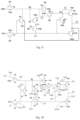
- FIG. 1 is a schematic view showing a driving circuitry of a display substrate according to one embodiment of the present disclosure
- FIG. 2 is another schematic view showing the driving circuitry of the display substrate according to one embodiment of the present disclosure
- FIG. 3 is a circuit diagram of the driving circuitry of the display substrate according to one embodiment of the present disclosure.
- FIG. 4 is a sequence diagram of the driving circuitry in FIG. 3 :
- FIG. 5 is another circuit diagram of the driving circuitry of the display substrate according to one embodiment of the present disclosure.
- FIG. 6 is a sequence diagram of the driving circuitry in FIG. 5 ;
- FIG. 7 is yet another circuit diagram of the driving circuitry of the display substrate according to one embodiment of the present disclosure.
- FIG. 8 is a sequence diagram of the driving circuitry in FIG. 7 ;
- FIG. 9 is still yet another circuit diagram of the driving circuitry of the display substrate according to one embodiment of the present disclosure.
- FIG. 10 is a circuit diagram of the driving circuitry according to one embodiment of the present disclosure, with reference signs of electrodes of transistors and electrode plates of capacitors;
- FIG. 11 is a schematic view showing the layout of the driving circuitry in
- FIG. 10
- FIG. 12 is a schematic view showing the layout of a semiconductor layer in FIG. 11 ;
- FIG. 13 is a schematic view showing the layout of a first gate metal layer in FIG. 11 ;
- FIG. 14 is a schematic view showing the layout of a second gate metal layer in FIG. 11 ;
- FIG. 15 is a schematic view showing the layout of a first source/drain metal layer in FIG. 11 ;
- FIG. 16 is a circuit diagram of the driving circuitry of the display substrate according to one embodiment of the present disclosure.
- FIG. 17 is a schematic view showing the layout of the driving circuitry in FIG. 11 with an additional light-shielding layer;
- FIG. 18 is a schematic view showing the layout of the light-shielding layer in FIG. 17 ;
- FIG. 19 is a schematic view showing the driving circuitry in FIG. 11 with an additional eleventh transistor;
- FIG. 20 is a schematic view showing a semiconductor layer in FIG. 19 ;
- FIG. 21 is a schematic view showing a first gate metal layer in FIG. 19 ;
- FIG. 22 is a schematic view showing a source/drain metal layer in FIG. 19 .
- All transistors adopted in the embodiments of the present disclosure may be triodes, thin film transistors (TFT), field effect transistors (FETs) or any other elements having an identical characteristic.
- TFT thin film transistors
- FETs field effect transistors
- the first electrode when the transistor is a TFT or FET, the first electrode may be a drain electrode and the second electrode may be a source electrode, or the first electrode may be a source electrode and the second electrode may be a drain electrode.
- the present disclosure provides in some embodiments a display substrate, which includes a driving circuitry arranged on a base substrate.
- the driving circuitry includes a first node control circuitry 11 , a second node control circuitry 12 and an output circuitry 13 .
- the first node control circuitry 11 is electrically coupled to a first node N 1 , an input end STV, a first clock signal line CK, a second clock signal line CB, a third node N 3 and a first voltage line V 1 , and configured to control a potential at the first node N 1 in accordance with an input signal from the input end STV and a first voltage signal from the first voltage line V 1 under the control of a first clock signal from the first clock signal line CK, a second clock signal from the second clock signal line CB and a potential at the third node N 3 .
- the second node control circuitry 12 is electrically coupled to a second node N 2 and the third node N 3 , and configured to control a potential at the second node N 2 and the potential at the third node N 3 .
- the output circuitry 13 is electrically coupled to the first node N 1 , the second node N 2 , a driving signal output end E 1 , the first voltage line V 1 and a second voltage line V 2 , and configured to control the driving signal output end E 1 to be electrically coupled to the second voltage line V 2 under the control of the potential at the first node N 1 , and control the driving signal output end E 1 to be electrically coupled to the first voltage line V 1 under the control of the potential at the second node N 2 .
- Transistors of the output circuitry 13 are arranged at a side of the second voltage line V 2 away from a display region, transistors of the first node control circuitry 11 and transistors of the second node control circuitry 12 are arranged at a side of the transistors of the output circuitry away from the second voltage line V 2 , and the first voltage line V 1 , the first clock signal line CK and the second clock signal line CB are arranged at a side of the transistors of the first node control circuitry 11 away from the second voltage line V 2 .
- the first voltage line is, but not limited to, a low voltage line
- the second voltage line is, but not limited to, a high voltage line.
- the first voltage line and the second voltage line are each a direct-current power source signal line.
- the first voltage line is configured to provide a first voltage signal
- the second voltage line is configured to provide a second voltage signal
- a value of the first voltage signal is smaller than a value of the second voltage signal.
- the present disclosure is not limited thereto.
- a line width of the first voltage line is greater than a line width of the second voltage line
- a line width of the first clock signal line is greater than the line width of the second voltage line
- a line width of the second clock signal line is greater than the line width of the second voltage line.
- the present disclosure is not limited thereto.
- a driving signal from the driving signal output end E 1 is, but not limited to, a light-emission control signal.
- the transistors of the driving circuitry are all n-type transistors.
- the driving circuitry has excellent driving capability and a simple circuit, and it may be used to meet the requirement on the all-oxide pixel driving.
- one capacitor element is reduced, so it is able to optimize a layout space.
- the n-type transistor when a gate-to-source voltage of the n-type transistor is greater than a threshold voltage of the n-type transistor, the n-type transistor is turned on, and when the gate-to-source voltage of the n-type transistor is smaller than the threshold voltage of the n-type transistor, the n-type transistor is turned off.
- the n-type transistor is, but not limited to, an oxide transistor, or an n-doped low-temperature polysilicon (LTPS) transistor.
- LTPS n-doped low-temperature polysilicon
- no capacitor electrically coupled to the first node N 1 is provided, because the output of the all-oxide driving circuitry is adversely affected due to the occurrence of a step in an output waveform of the all-oxide driving circuitry when the capacitor is used for the all-oxide driving circuitry. Due to the absence of the capacitor, it is able to optimize the layout space of the driving circuitry.
- the transistors of the output circuitry 13 are arranged at the side of the second voltage line V 2 away from the display region, the transistors of the first node control circuitry 11 and transistors of the second node control circuitry 12 are arranged at the side of the transistors of the output circuitry 13 away from the second voltage line V 2 , and the first voltage line V 1 , the first clock signal line CK and the second clock signal line CB are arranged at the side of the transistors of the first node control circuitry 11 away from the second voltage line V 2 .
- the transistors of the first node control circuitry 11 , the transistor of the second node control circuitry 12 and the transistors of the output circuitry 13 are arranged between the first voltage line V 1 and the second voltage line V 2 , so as to facilitate the layout.
- the transistors of the second node control circuitry are arranged between the transistors of the first node control circuitry and the transistors of the output circuitry.
- the transistors of the second node control circuitry are arranged between the transistors of the first node control circuitry and the transistors of the output circuitry, and the transistors of the first node control circuitry are arranged sequentially in a first direction, so as to reduce a space occupied in a transverse direction, thereby to provide a narrow bezel.
- the first direction is, but not limited to, a vertical direction.
- the first node control circuitry includes a first transistor, a second transistor and a third transistor.
- a first gate electrode of the first transistor is electrically coupled to the first clock signal line, a first electrode of the first transistor is electrically coupled to the input end, and a second electrode of the first transistor is electrically coupled to the first node.
- a first gate electrode of the second transistor is electrically coupled to the second clock signal line, a first electrode of the second transistor is electrically coupled to a second electrode of the third transistor, and a second electrode of the second transistor is electrically coupled to the first node.
- a first gate electrode of the third transistor is electrically coupled to the third node, and a first electrode of the third transistor is electrically coupled to the first voltage line.
- the first node control circuitry includes the first transistor, the second transistor and the third transistor.
- the first transistor is configured to control the input end to be electrically coupled to the first node under the control of the first clock signal
- the second transistor is configured to control the second electrode of the third transistor to be electrically coupled to the first node under the control of the second clock signal
- the third transistor is configured to control the first voltage line to be electrically coupled to the second electrode of the third transistor under the control of the potential at the third node, thereby to control the potential at the first node.
- the first voltage line, the second voltage line, the first clock signal line and the second clock signal line extend in a first direction.
- the first transistor, the second transistor and the third transistor are arranged sequentially in the first direction, so as to reduce the space in the transverse direction, thereby to provide a narrow bezel.
- the first direction is, but not limited to, a vertical direction.
- the second node control circuitry includes a third node control sub-circuitry 21 , a fourth node control sub-circuitry 22 and a second node control sub-circuitry 23 .
- the third node N 3 control sub-circuitry 21 is electrically coupled to the third node N 3 , the second voltage line V 2 , the first clock signal end CK and the first node N 1 , and configured to control the third node N 3 to be electrically coupled to the second voltage line V 2 under the control of the first clock signal, and control the third node N 3 to be electrically coupled to the first clock signal line CK under the control of the potential at the first node N 1 .
- the fourth node control sub-circuitry 22 is electrically coupled to the third node N 3 , the second clock signal line CB and a fourth node N 4 , and configured to control the fourth node N 4 to be electrically coupled to the second clock signal line CB under the control of the potential at the third node N 3 , and control a potential at the fourth node N 4 in accordance with the potential at the third node N 3 .
- the second node control sub-circuitry 23 is electrically coupled to the second clock signal line CB, the fourth node N 4 , the second node N 2 , the first node N 1 and the first voltage line V 1 , and configured to control the second node N 2 to be electrically coupled to the fourth node N 4 under the control of the second clock signal, control the second node N 2 to be electrically coupled to the first voltage line V 1 under the control of the potential at the first node N 1 , and maintain the potential at the second node N 2 .
- the third node control sub-circuitry 21 controls the potential at the third node N 3 under the control of the first clock signal and the potential at the first node N 1
- the fourth node control sub-circuitry 22 controls the potential at the fourth node N 4 under the control of the potential at the third node N 3
- the second node control sub-circuitry 23 controls the potential at the second node N 2 under the control of the second clock signal and the potential at the first node N 1 .
- the third node control sub-circuitry includes a fourth transistor and a fifth transistor.
- a first gate electrode of the fourth transistor is electrically coupled to the first clock signal line, a first electrode of the fourth transistor is electrically coupled to the second voltage line, and a second electrode of the fourth transistor is electrically coupled to the third node.
- a first gate electrode of the fifth transistor is electrically coupled to the first node, a first electrode of the fifth transistor is electrically coupled to the first clock signal line, and a second electrode of the fifth transistor is electrically coupled to the third node.
- the fourth node control sub-circuitry includes a sixth transistor and a first capacitor.
- a first gate electrode of the sixth transistor is electrically coupled to the third node, a first electrode of the sixth transistor is electrically coupled to the second clock signal line, and a second electrode of the sixth transistor is electrically coupled to the fourth node.
- a first electrode plate of the first capacitor is electrically coupled to the third node, and a second electrode plate of the first capacitor is electrically coupled to the fourth node.
- the second node control sub-circuitry includes a seventh transistor, an eighth transistor and a second capacitor.
- a first gate electrode of the seventh transistor is electrically coupled to the second clock signal line, a first electrode of the seventh transistor is electrically coupled to the fourth node, and a second electrode of the seventh transistor is electrically coupled to the second node.
- a first gate electrode of the eighth transistor is electrically coupled to the first node, a first electrode of the eighth transistor is electrically coupled to the first voltage line, and a second electrode of the eighth transistor is electrically coupled to the second node.
- a first electrode plate of the second capacitor is electrically coupled to the second node, and a second electrode plate of the second capacitor is electrically coupled to the first voltage line.
- the output circuitry includes a ninth transistor and a tenth transistor.
- a first gate electrode of the ninth transistor is electrically coupled to the fourth node, a first electrode of the ninth transistor is electrically coupled to the first voltage line, and a second electrode of the ninth transistor is electrically coupled to the driving signal output end.
- a first gate electrode of the tenth transistor is electrically coupled to the first node, a first electrode of the tenth transistor is electrically coupled to the second voltage line, and a second electrode of the tenth transistor is electrically coupled to the driving signal output end.
- the driving circuitry further includes a third capacitor, a first electrode plate of which is electrically coupled to the first node, and a second electrode plate of which is electrically coupled to the second clock signal line.
- the driving circuitry further includes a potential control circuitry electrically coupled to the first node, and configured to control the potential at the first node to be smaller than a control voltage threshold, so as to reduce a bias voltage of a transistor whose gate electrode is electrically coupled to the first node, thereby to prevent the occurrence of a drift for a threshold voltage of the transistor.
- the potential control circuitry includes an eleventh transistor, a gate electrode and a first electrode of which are electrically coupled to the first node, and a second electrode of which is electrically coupled to the second voltage line.
- the first node control circuitry 11 includes a first transistor T 1 , a second transistor T 2 and a third transistor T 3 .
- a first gate electrode of the first transistor T 1 is electrically coupled to the first clock signal line CK
- a source electrode of the first transistor T 1 is electrically coupled to the input end STV
- a drain electrode of the first transistor T 1 is electrically coupled to the first node N 1 .
- a first gate electrode of the second transistor T 2 is electrically coupled to the second clock signal line CB, a source electrode of the second transistor T 2 is electrically coupled to a drain electrode of the third transistor T 3 , and a drain electrode of the second transistor T 2 is electrically coupled to the first node N 1 .
- a first gate electrode of the third transistor T 3 is electrically coupled to the third node N 3 , and a source electrode of the third transistor T 3 is electrically coupled to a low voltage line VGL.
- the third node control sub-circuitry 21 includes a fourth transistor T 4 and a fourth transistor T 5 .
- a first gate electrode of the fourth transistor T 4 is electrically coupled to the first clock signal line CK
- a source electrode of the fourth transistor T 4 is electrically coupled to a high voltage line VGH
- a drain electrode of the fourth transistor T 4 is electrically coupled to the third node N 3 .
- a first gate electrode of the fourth transistor T 5 is electrically coupled to the first node N 1
- a source electrode of the fourth transistor T 5 is electrically coupled to the first clock signal line CK
- a drain electrode of the fourth transistor T 5 is electrically coupled to the third node N 3 .
- the fourth node control sub-circuitry 22 includes a sixth transistor T 6 and a first capacitor C 1 .
- a first gate electrode of the sixth transistor T 6 is electrically coupled to the third node N 3
- a source electrode of the sixth transistor T 6 is electrically coupled to the second clock signal line CB
- a drain electrode of the sixth transistor T 6 is electrically coupled to the fourth node N 4 .
- a first electrode plate of the first capacitor C 1 is electrically coupled to the third node N 3
- a second electrode plate of the first capacitor C 1 is electrically coupled to the fourth node N 4 .
- the second node control sub-circuitry 23 includes a seventh transistor T 7 , an eighth transistor T 8 and a second capacitor C 2 .
- a first gate electrode of the seventh transistor T 7 is electrically coupled to the second clock signal line CB, a source electrode of the seventh transistor T 7 is electrically coupled to the fourth node N 4 , and a drain electrode of the seventh transistor T 7 is electrically coupled to the second node N 2 .
- a first gate electrode of the eighth transistor T 8 is electrically coupled to the first node N 1 , a source electrode of the eighth transistor T 8 is electrically coupled to the low voltage line VGL, and a drain electrode of the eighth transistor T 8 is electrically coupled to the second node N 2 .
- a first electrode plate of the second capacitor C 2 is electrically coupled to the second node N 2 , and a second electrode plate of the second capacitor C 2 is electrically coupled to the low voltage line VGL.
- the output circuitry 13 includes a ninth transistor T 9 and a tenth transistor T 10 .
- a first gate electrode of the ninth transistor T 9 is electrically coupled to the fourth node N 4
- a source electrode of the ninth transistor T 9 is electrically coupled to the low voltage line VGL
- a drain electrode of the ninth transistor T 9 is electrically coupled to the driving signal output end E 1 .
- a first gate electrode of the tenth transistor T 10 is electrically coupled to the first node N 1
- a source electrode of the tenth transistor T 10 is electrically coupled to the high voltage line VGH
- a drain electrode of the tenth transistor T 10 is electrically coupled to the driving signal output end E 1 .
- the first voltage line is, but not limited to, the low voltage line VGL
- the second voltage line is, but not limited to, the high voltage line VGH.
- the low voltage line VGL is configured to provide a low voltage signal
- the high voltage line VGH is configured to provide a high voltage signal
- a value of the low voltage signal from the low voltage line VGL is smaller than a value of the high voltage signal from the high voltage line VGH.
- the present disclosure is limited thereto.
- all the transistors are n-type transistors, e.g., Indium Gallium Zinc Oxide (IGZO) transistors.
- IGZO Indium Gallium Zinc Oxide
- the present disclosure is not limited thereto, and in actual use, all the transistors may also be n-doped LTPS transistors.
- N 5 represents the fifth node.
- FIG. 4 is a sequence diagram of the driving circuitry in FIG. 3 .
- a display period includes a first stage t 1 , a second stage 12 , a third stage t 3 , a fourth stage 15 , a fifth stage ( 5 , a sixth stage 16 , a seventh stage t 7 and an eight stage 18 arranged sequentially.
- STV provides a low voltage signal
- CK provides a high voltage signal
- CB provides a low voltage signal.
- T 4 is turned on to enable a potential at N 3 to be a high voltage
- T 1 is turned on to enable a potential at N 1 to be a low voltage
- T 6 is turned on to enable a potential at N 4 to be a low voltage
- T 3 is turned on to enable a potential at N 5 to be a low voltage
- T 7 and T 8 are turned off to maintain a potential at N 2 to be a low voltage
- T 9 is turned off and T 10 is turned on to enable E 1 to output a high voltage signal.
- STV provides a low voltage signal
- CK provides a low voltage signal
- CB provides a high voltage signal.
- T 1 and T 4 are turned off to maintain the potential at N 3 to be a high voltage
- T 2 and T 3 are turned on to enable the potential at N 1 to be a low voltage
- T 6 and T 7 are turned on to control the potential at N 2 and the potential at N 4 to be each a high voltage and enable the potential at N 5 to be a low voltage
- T 9 is turned on and T 10 is turned off to enable E 1 to output a low voltage signal.
- STV provides a low voltage signal
- CK provides a high voltage signal
- CB provides a low voltage signal.
- T 1 and T 4 are turned on to enable the potential at N 3 to be a high voltage
- T 3 is turned on and T 2 is turned off to enable the potential at N 5 to be a low voltage and enable the potential at N 1 to be a low voltage
- T 6 is turned on
- T 7 is turned off and T 8 is turned off to maintain the potential at N 2 to be a high voltage
- T 9 is turned on and T 10 is turned off to enable E 1 to output a low voltage signal.
- STV provides a low voltage signal
- CK provides a low voltage signal
- CB provides a high voltage signal.
- T 1 and T 4 are turned off to enable the potential at N 3 to be a high voltage
- T 2 and T 3 are turned on to enable the potential at N 1 to be a low voltage
- T 6 and T 7 are turned on to enable the potential at N 2 to be a high voltage and enable the potential at N 5 to be a low voltage
- T 9 is turned on and T 10 is turned off to enable E 1 to output a low voltage signal.
- STV provides a low voltage signal
- CK provides a high voltage signal
- CB provides a low voltage signal.
- T 1 and T 4 are turned on to enable the potential at N 3 to be a high voltage
- T 3 is turned on and T 2 is turned off to enable the potential at N 5 to be a low voltage and enable the potential at N 1 to be a low voltage
- T 6 is turned on
- T 7 is turned off and T 8 is turned off to maintain the potential at N 2 to be a high voltage
- T 9 is turned on and T 10 is turned off to enable E 1 to output a low voltage signal.
- STV provides a low voltage signal
- CK provides a low voltage signal
- CB provides a high voltage signal.
- T 1 and T 4 are turned off to enable the potential at N 3 to be a high voltage
- T 2 and T 3 are turned on to enable the potential at N 1 to be a low voltage
- T 6 and T 7 are turned on to enable the potential at N 2 to be a high voltage and enable the potential at N 5 to be a low voltage
- T 9 is turned on and T 10 is turned off to enable E 1 to output a low voltage signal.
- STV provides a high voltage signal
- CK provides a high voltage signal
- CB provides a low voltage signal.
- T 1 and T 4 are turned on to enable the potential at N 1 to be a high voltage and enable the potential at N 3 to be a high voltage
- T 5 is turned on
- T 2 is turned off and T 3 is turned on to enable the potential at N 5 to be a low voltage
- T 7 is turned off and T 8 is turned on to enable the potential at N 2 to be a low voltage
- T 9 is turned off and T 10 is turned on to enable E 1 to output a high voltage signal.
- STV provides a low voltage signal.
- CK provides a low voltage signal
- CB provides a high voltage signal.
- T 1 and T 4 are turned off to enable the potential at N 1 to be a high voltage
- T 5 is turned on to enable the potential at N 3 to be a low voltage
- T 6 is turned off
- T 7 is turned on and T 8 is turned on to enable the potential at N 2 to be a low voltage
- T 9 is turned off and T 10 is turned on to enable E 1 to output a high voltage signal.
- Vn 1 represents the potential at N 1
- Vn 2 represents the potential at N 2
- Vn 3 represents the potential at N 3
- Vn 4 represents the potential at N 4
- Vn 5 represents the potential at N 5 .
- the driving circuitry further includes a third capacitor C 3 , a first electrode plate of which is electrically coupled to the first node N 1 , and a second electrode plate of which is electrically coupled to the second clock signal line CB.
- FIG. 6 is a sequence diagram of the driving circuitry in FIG. 5 .
- Vn 1 represents the potential at N 1
- Vn 2 represents the potential at N 2
- Vn 3 represents the potential at N 3
- Vn 4 represents the potential at N 4
- Vn 5 represents the potential at N 5 .
- the driving circuitry further includes a potential control circuitry 60 electrically coupled to the first node N 1 and configured to control the potential at the first node N 1 to be smaller than a control voltage threshold.
- the potential control circuitry 60 includes an eleventh transistor T 11 , a gate electrode and a source electrode of which are electrically coupled to the first node N 1 , and a drain electrode of which is electrically coupled to the high voltage line VGH.
- FIG. 8 is a sequence diagram of the driving circuitry in FIG. 7 .
- T 11 is turned on to control the first node N 1 to be electrically coupled to the high voltage line VGH, so as to pull down the potential at the first node N 1 and reduce a bias voltage applied to T 10 , thereby to prevent the occurrence of a drift for a threshold voltage of T 10 and improve a driving effect, where Vth 11 represents a threshold voltage of T 11 .
- T 1 , T 2 , T 3 , T 4 , T 5 , T 6 , T 7 , T 8 , T 9 and T 10 are all double-gate transistors.
- a second gate electrode of the first transistor T 1 is electrically coupled to the low voltage line VGL
- a second gate electrode of the second transistor T 2 is electrically coupled to the low voltage line VGL
- a second gate electrode of the third transistor T 3 is electrically coupled to the low voltage line VGL.
- a second gate electrode of the fourth transistor T 4 is electrically coupled to the low voltage line VGL
- a second gate electrode of the fifth transistor T 5 is electrically coupled to the a second gate electrode of the tenth transistor T 10
- the second gate electrode of the tenth transistor T 10 is electrically coupled to the drain electrode of the tenth transistor T 10 .
- a second gate electrode of the sixth transistor T 6 is electrically coupled to the low voltage line VGL
- a second gate electrode of the seventh transistor T 7 is electrically coupled to the first gate electrode of the tenth ninth T 9
- the second gate electrode of the eighth transistor T 8 is electrically coupled to a second gate electrode of the ninth transistor T 9
- the second gate electrode of the ninth transistor T 9 is electrically coupled to the low voltage line VGL.
- FIG. 10 is a circuit diagram of the driving circuitry, with reference signs of the electrodes of the transistors and the electrode plates of the capacitors.
- the first node control circuitry includes a first transistor T 1 , a second transistor T 2 and a third transistor T 3 .
- a first gate electrode G 11 of the first transistor T 1 is electrically coupled to the first clock signal line CK
- a first electrode S 1 of the first transistor T 1 is electrically coupled to the input end STV
- a second electrode D 1 of the first transistor T 1 is electrically coupled to a second electrode D 2 of the second transistor T 2 .
- a first gate electrode G 21 of the second transistor T 2 is electrically coupled to the second clock signal line CB, a first electrode S 2 of the second transistor T 2 is electrically coupled to a second electrode D 3 of the third transistor T 3 , and the second electrode D 2 of the second transistor T 2 is electrically coupled to the first node N 1 .
- a first gate electrode G 31 of the third transistor T 3 is electrically coupled to the second electrode D 2 of the second transistor T 2 , and a first electrode S 3 of the third transistor T 3 is electrically coupled to the low voltage line VGL.
- the third node control sub-circuitry includes a fourth transistor T 5 and a fifth transistor T 5 .
- a first gate electrode G 41 of the fourth transistor T 4 is electrically coupled to the first clock signal line CK
- a first electrode S 4 of the fourth transistor T 4 is electrically coupled to the high voltage line VGH
- a second electrode D 4 of the fourth transistor T 4 is electrically coupled to a second electrode D 5 of the fifth transistor T 5 .
- a first gate electrode G 51 of the fifth transistor T 5 is electrically coupled to the first node N 1
- a first electrode S 5 of the fifth transistor T 5 is electrically coupled to the first clock signal line CK
- the second electrode D 5 of the fifth transistor T 5 is electrically coupled to the third node N 3 .
- the fourth node control sub-circuitry includes a sixth transistor T 6 and a first capacitor C 1 .
- a first gate electrode G 61 of the sixth transistor T 6 is electrically coupled to the third node N 3
- a source electrode S 6 of the sixth transistor T 6 is electrically coupled to the second clock signal line CB
- a drain electrode D 6 of the sixth transistor T 6 is electrically coupled to the fourth node N 4 .
- a first electrode plate C 1 a of the first capacitor C 1 is electrically coupled to the third node N 3
- a second electrode plate C 1 b of the first capacitor C 1 is electrically coupled to the fourth node N 4 .
- the second node control sub-circuitry includes a seventh transistor T 7 , an eighth transistor T 8 and a second capacitor C 2 .
- a first gate electrode G 71 of the seventh transistor T 7 is electrically coupled to the second clock signal line CB
- a first electrode S 7 of the seventh transistor T 7 is electrically coupled to the fourth node N 4
- a second electrode D 7 of the seventh transistor T 7 is electrically coupled to the second node N 2 .
- a first gate electrode G 81 of the eighth transistor T 8 is electrically coupled to the first node N 1
- a first electrode S 8 of the eighth transistor T 8 is electrically coupled to the low voltage line VGL
- a second electrode D 8 of the eighth transistor T 8 is electrically coupled to the second node N 2 .
- a first electrode plate C 2 a of the second capacitor C 2 is electrically coupled to the second node N 2
- a second electrode plate C 2 b of the second capacitor C 2 is electrically coupled to the low voltage line VGL.
- the output circuitry 13 includes a ninth transistor T 9 and a tenth transistor T 10 .
- a first gate electrode G 91 of the ninth transistor T 9 is electrically coupled to the fourth node N 4
- a first electrode S 9 of the ninth transistor T 9 is electrically coupled to the low voltage line VGL
- a second electrode D 9 of the ninth transistor T 9 is electrically coupled to the driving signal output end E 1 .
- a first gate electrode G 101 of the tenth transistor T 10 is electrically coupled to the first node N 1
- a first electrode S 10 of the tenth transistor T 10 is electrically coupled to the high voltage line VGH
- a second electrode D 10 of the tenth transistor T 10 is electrically coupled to the driving signal output end E 1 .
- the first voltage line is the low voltage line VGL
- the second voltage line is the high voltage line VGH.
- the display substrate includes a semiconductor layer, a first gate metal layer and a source/drain metal layer laminated one on another in a direction away from the base substrate.
- the first gate electrode of the first transistor is formed integrally with a first conductive connection member, and the first conductive connection member is coupled to the first clock signal line.
- the first electrode of the first transistor is coupled to a second conductive connection member, and the second conductive connection member is coupled to the input end.
- the second electrode of the first transistor is coupled to a third conductive connection member, and the third conductive connection member is coupled to the second electrode of the second transistor.
- the first electrode of the third transistor is coupled to a fourth conductive connection member, and the fourth conductive connection member is formed integrally with the first voltage line.
- An active layer of the first transistor includes the first electrode and the second electrode of the first transistor
- an active layer of the second transistor includes the first electrode and the second electrode of the second transistor
- an active layer of the third transistor includes the first electrode and the second electrode of the third transistor.
- the active layer of the first transistor, the active layer of the second transistor and the active layer of the third transistor are included in the semiconductor layer
- the first gate electrode of the first transistor, the first gate electrode of the second transistor and the first gate electrode of the third transistor are included in the first gate metal layer
- the input end and the first conductive connection member are included in the first gate metal layer
- the second conductive connection member, the third conductive connection member and the fourth conductive connection member are included in the source/drain metal layer.
- FIG. 11 shows the layout of the driving circuitry in FIG. 10
- FIG. 12 shows the layout of the semiconductor layer in FIG. 11
- FIG. 13 shows the layout of the first gate metal layer in FIG. 11
- FIG. 14 shows the layout of the second gate metal layer in FIG. 11
- FIG. 15 shows the layout of a first source/drain metal layer in FIG. 11 .
- the first gate electrode G 11 of the first transistor T 1 and a first conductive connection member L 1 are formed integrally, and the first conductive connection member L 1 is coupled to the first clock signal line CK.
- the first electrode S 1 of the first transistor T 1 is coupled to a second conductive connection member L 2 , and the second conductive connection member L 2 is coupled to the input end STV.
- the second electrode D 1 of the first transistor T 1 is coupled to a third conductive connection member L 3 , and the third conductive connection member L 3 is coupled to the second electrode D 2 of the second transistor T 2 .
- the first electrode S 3 of the third transistor T 3 is coupled to a fourth conductive connection member L 4 , and the fourth conductive connection member L 4 is formed integrally with the low voltage line VGL.
- An active layer of the first transistor T 1 includes the first electrode S 1 , a channel region and the second electrode D 1 of the first transistor T 1
- an active layer of the second transistor T 2 includes the first electrode S 2 , a channel region and the second electrode D 2 of the second transistor
- an active layer of the third transistor T 3 includes the first electrode S 3 , a channel region and the second electrode D 3 of the third transistor T 3 .
- the channel region of T 1 is arranged between S 1 and D 1
- the channel region of T 2 is arranged between S 2 and D 2
- the channel region of T 3 is arranged between S 3 and D 3 .
- the active layer of the first transistor T 1 , the active layer of the second transistor T 2 and the active layer of the third transistor T 3 are included in the semiconductor layer.
- the first gate electrode G 11 of the first transistor T 1 , the first gate electrode G 21 of the second transistor T 2 and the first gate electrode G 31 of the third transistor T 3 are included in the first gate metal layer, and the input end STV and the first conductive connection member L 1 are included in the first gate metal layer.
- the second conductive connection member L 2 , the third conductive connection member L 3 and the fourth conductive connection member L 4 are included in the source/drain metal layer.
- the display substrate includes a semiconductor layer, a first gate metal layer, a second gate metal layer and a source/drain metal layer laminated one on another in a direction away from the base substrate.
- the first gate electrode G 41 of the fourth transistor T 4 , a first conductive connection member L 1 and a fifth conductive connection member L 5 are formed integrally, the first conductive connection member L 1 is coupled to the first clock signal line CK, the fifth conductive connection member L 5 is coupled to a sixth conductive connection member L 6 , and the sixth conductive connection member L 6 is coupled to the first electrode S 5 of the fifth transistor T 5 .
- the first gate electrode G 21 of the second transistor T 2 , the first gate electrode G 71 of the seventh transistor T 7 , a seventh conductive connection member L 7 and an eighth conductive connection member L 8 are formed integrally, the seventh conductive connection member L 7 is coupled to the second clock signal line CB, the eighth conductive connection member L 8 is coupled to a ninth conductive connection member L 9 , the ninth conductive connection member L 9 is coupled to the first electrode S 6 of the sixth transistor T 6 , the second electrode D 6 of the sixth transistor T 6 is coupled to a tenth conductive connection member L 10 , and the tenth conductive connection member L 10 is coupled to the second electrode plate C 1 b of the first capacitor C 1 .
- the first gate electrode G 31 of the third transistor T 3 , the first gate electrode G 61 of the sixth transistor T 6 , the first electrode C 1 a of the first capacitor C 1 and an eleventh conductive connection member L 11 are formed integrally, the eleventh conductive connection member L 11 is coupled to a twelfth conductive connection member L 12 , and the twelfth conductive connection member L 12 is coupled to the second electrode D 4 of the fourth transistor T 4 and the second electrode D 5 of the fifth transistor T 5 .
- the first gate electrode G 51 of the fifth transistor T 5 , the first gate electrode G 81 of the eighth transistor T 8 , the first gate electrode of the tenth transistor T 10 and a thirteenth conductive connection member L 13 are formed integrally, and the thirteenth conductive connection member L 13 is coupled to a third conductive connection member L 3 .
- the first gate electrode of the tenth transistor T 10 includes a first gate electrode pattern G 111 , a second gate electrode pattern G 112 , a third gate electrode pattern G 113 , a fourth gate electrode pattern G 114 , a fifth gate electrode pattern G 115 , a sixth gate electrode pattern G 116 , a seventh gate electrode pattern G 117 , an eighth gate electrode pattern G 118 , a ninth gate electrode pattern G 119 and a tenth gate electrode pattern G 1110 electrically coupled to each other.
- the first electrode S 4 of the fourth transistor T 4 is coupled to a fourteenth conductive connection member L 14 , and the fourteenth conductive connection member L 14 and the high voltage line VGH are formed integrally.
- the first electrode S 7 of the seventh transistor T 7 is adjacent to and continuous with the second electrode D 6 of the sixth transistor T 6 , and the first gate electrode of the ninth transistor T 9 and a fifteenth conductive connection member L 15 are formed integrally.
- the first gate electrode of the ninth transistor T 9 includes an eleventh gate electrode pattern G 1111 , a twelfth gate electrode pattern G 1112 , a thirteenth gate electrode pattern G 1113 , a fourteenth gate electrode pattern G 1114 , a fifteenth gate electrode pattern G 1115 , a sixteenth gate electrode pattern G 1116 , a seventeenth gate electrode pattern G 1117 , an eighteenth gate electrode pattern G 1118 , a nineteenth gate electrode pattern G 1119 and a twentieth gate electrode pattern G 1120 .
- the second electrode D 7 of the seventh transistor T 7 is coupled to a sixteenth conducive connection member L 16
- the sixteenth conductive connection member L 16 is coupled to the second electrode D 8 of the eighth transistor T 8 and the fifteenth conductive connection member L 15 .
- the first electrode S 8 of the eighth transistor T 8 is coupled to the first electrode S 9 of the ninth transistor T 9 , the first gate electrode of the ninth transistor T 9 and the first electrode plate C 2 a of the second capacitor C 2 are formed integrally, the second electrode plate C 2 b of the second capacitor C 2 is coupled to a seventeenth conductive connection member L 17 , and the seventeenth conductive connection member L 17 and the low voltage line VGL are formed integrally.
- An active layer of the fourth transistor T 4 includes the first electrode S 4 and the second electrode D 4 of the fourth transistor T 4
- an active layer of the fifth transistor T 5 includes the first electrode S 5 and the second electrode D 5 of the fifth transistor T 5
- an active layer of the sixth transistor T 6 includes the first electrode S 6 and the second electrode D 6 of the sixth transistor T 6
- an active layer of the seventh transistor T 7 includes the first electrode S 7 and the second electrode D 7 of the seventh transistor T 7
- an active layer of the eighth transistor T 8 includes the first electrode S 8 and the second electrode D 8 of the eighth transistor T 8 .
- the active layer of the fourth transistor T 4 , the active layer of the fifth transistor T 5 , the active layer of the sixth transistor T 6 , the active layer of the seventh transistor T 7 and the active layer of the eighth transistor T 8 are included in the semiconductor layer.
- the first gate electrode G 41 of the fourth transistor T 4 , the first gate electrode G 51 of the fifth transistor T 6 , the first gate electrode G 61 of the sixth transistor T 6 , the first gate electrode G 71 of the seventh transistor T 7 and the first gate electrode G 81 of the eighth transistor T 8 are included in the first gate metal layer.
- the first electrode plate C 1 a of the first capacitor C 1 and the first electrode plate C 2 a of the second capacitor C 2 are included in the first gate metal layer, and the second gate electrode C 1 b of the first capacitor C 1 and the second gate electrode C 2 b of the second capacitor C 2 are included in the second gate metal layer.
- the first clock signal line CK, the second clock signal line CB, the low voltage line VGL and the high voltage line VGH are included in the source/drain metal layer.
- the fifth conductive connection member L 5 , the seventh conductive connection member L 7 , the eighth conductive connection member L 8 , the eleventh conductive connection member L 11 , the thirteenth conductive connection member L 13 and the fifteenth conductive connection member L 15 are included in the first gate metal layer.
- the sixth conductive connection member L 6 , the ninth conductive connection member L 9 , the tenth conductive connection member L 10 , the twelfth conductive connection member L 12 , the fourteenth conductive connection member L 14 , the sixteenth conductive connection member L 16 and the seventeenth conductive connection member L 17 are included in the source/drain metal layer.
- a line width K 1 of the low voltage line VGL is greater than a line width K 2 of the high voltage line VGH
- a line width K 3 of the first clock signal line CK is greater than the line width K 2 of the high voltage line VGH
- a line width K 4 of the second clock signal line CB is greater than the line width K 2 of the high voltage line VGH.
- a line width K 0 of a start signal line E 0 is smaller than the line width K 1 of the low voltage line VGL, the line width K 3 of the first clock signal line CK, and the line width K 4 of the second clock signal line CB.
- the present disclosure is not limited thereto.
- the tenth transistor and the ninth transistor are arranged in a first direction, and an active layer of the ninth transistor is continuous with an active layer of the tenth transistor.
- the first electrode and the second electrode of the tenth transistor and the first electrode and the second electrode of the ninth transistor are included in the source/drain metal layer.
- the first gate electrode of the tenth transistor and the first gate electrode of the ninth transistor are included in the first gate metal layer.
- the first electrode of the tenth transistor, the fourteenth conductive connection member and the second voltage line are formed integrally.
- the second electrode of the tenth transistor and the second electrode of the ninth transistor are formed integrally.
- the second electrode of the ninth transistor is coupled to the driving signal output end, and the driving signal output signal is included in the first gate metal layer.
- the first electrode of the ninth transistor and the first voltage line are formed integrally.
- an active layer of the ninth transistor T 9 includes a first active member A 1 and a second active member A 2
- an active layer of the tenth transistor T 10 includes a third active member A 3 and a fourth active member A 2
- the first active member A 1 is continuous with the third active member A 3
- the second active member A 2 is continuous with the fourth active member A 4 .
- the first electrode S 10 and the second electrode D 10 of the tenth transistor T 10 and the first electrode S 9 and the second electrode D 9 of the ninth transistor T 9 are included in the source/drain metal layer.
- the first gate electrode of the tenth transistor T 10 and the first gate electrode of the ninth transistor T 9 are included in the first gate metal layer.
- the first electrode S 10 of the tenth transistor T 10 , the fourteenth conductive connection member L 14 and the high voltage line VGH are formed integrally.
- the second electrode D 10 of the tenth transistor T 10 and the second electrode D 9 of the ninth transistor T 9 are formed integrally, the second electrode D 9 of the ninth transistor T 9 is coupled to the driving signal output end E 1 , and the driving signal output end E 1 is included in the first gate metal layer.
- the first electrode S 9 of the ninth transistor T 9 and the low voltage line VGL are formed integrally.
- the active layer of the ninth transistor T 9 and the active layer of the tenth transistor T 10 include two active portions, one including the first active member A 1 and the third active member A 3 continuous with each other, the other including the second active member A 2 and the fourth active member A 4 continuous with each other.
- the active layer of the ninth transistor T 9 and the active layer of the tenth transistor T 10 may be provided with at least two active portions.
- E 0 represents a start signal line.
- the first transistor, the second transistor and the third transistor are double-gate transistors.
- a second gate electrode of the first transistor is electrically coupled to the first voltage line
- a second gate electrode of the second transistor is electrically coupled to the first voltage line
- a second gate electrode of the third transistor is electrically coupled to the first voltage line.
- the display substrate further includes a light-shielding layer arranged between the base substrate and the semiconductor layer, and the second gate electrode of the first transistor, the second gate electrode of the second transistor and the second gate electrode of the third transistor are included in the light-shielding layer.
- the light-shielding layer is further configured to shield light
- the first gate electrode is a top gate electrode
- the second gate electrode is a bottom gate electrode.
- the first transistor T 1 , the second transistor T 2 and the third transistor T 3 are all double-gate transistors.
- the second gate electrode G 12 of the first transistor T 1 is electrically coupled to the low voltage line VGL
- the second gate electrode G 22 of the second transistor T 2 is electrically coupled to the low voltage line VGL
- the second gate electrode G 32 of the third transistor T 3 is electrically coupled to the low voltage line VGL.
- the display substrate further includes the light-shielding layer arranged between the base substrate and the semiconductor layer, and the second gate electrode G 12 of the first transistor T 1 , the second gate electrode G 22 of the second transistor T 2 and the second gate electrode G 32 of the third transistor T 3 are included in the light-shielding layer.
- FIG. 17 shows the layer of the driving circuitry in FIG. 11 with the additional light-shielding layer
- FIG. 18 shows the layout of the light-shielding layer in FIG. 17 .
- E 0 represents the start signal line.
- the fourth transistor, the fifth transistor, the sixth transistor, the seventh transistor, the eighth transistor, the ninth transistor and the tenth transistor are double-gate transistors.
- a second gate electrode of the fourth transistor is electrically coupled to the first voltage line
- a second gate electrode of the fifth transistor is electrically coupled to a second gate electrode of the tenth transistor
- the second gate electrode of the tenth transistor is electrically coupled to the second electrode of the tenth transistor.
- a second gate electrode of the sixth transistor is electrically coupled to the first voltage line
- a second gate electrode of the seventh transistor is electrically coupled to the first gate electrode of the ninth transistor
- a second gate electrode of the eighth transistor is electrically coupled to a second gate electrode of the ninth transistor
- the second gate electrode of the ninth transistor is electrically coupled to the first voltage line.
- the second gate electrode of the fourth transistor, the second gate electrode of the fifth transistor, the second gate electrode of the sixth transistor, the second gate electrode of the seventh transistor, the second gate electrode of the eighth transistor, the second gate electrode of the ninth transistor and the second gate electrode of the tenth transistor are included in the light-shielding layer.
- the fourth transistor T 4 , the fifth transistor T 5 , the sixth transistor T 6 , the seventh transistor T 7 , the eighth transistor T 8 , the ninth transistor T 9 and the tenth transistor T 10 are double-gate transistors.
- the second gate electrode G 42 of the fourth transistor T 4 is electrically coupled to the low voltage line VGL
- the second gate electrode G 52 of the fifth transistor T 5 is electrically coupled to the second gate electrode G 102 of the tenth transistor T 10
- the second gate electrode G 102 of the tenth transistor T 10 is electrically coupled to the second electrode D 10 of the tenth transistor T 10 .
- the second gate electrode G 62 of the sixth transistor T 6 is electrically coupled to the low voltage line VGL
- the second gate electrode G 72 of the seventh transistor T 7 is electrically coupled to the first gate electrode G 91 of the ninth transistor T 9
- the second gate electrode G 82 of the eighth transistor T 8 is electrically coupled to the second gate electrode G 92 of the ninth transistor T 9
- the second gate electrode G 92 of the ninth transistor T 9 is electrically coupled to the low voltage line VGL.
- the second gate electrode G 42 of the fourth transistor T 4 the second gate electrode G 52 of the fifth transistor T 5 , the second gate electrode G 62 of the sixth transistor T 6 , the second gate electrode G 72 of the seventh transistor T 7 , the second gate electrode G 82 of the eighth transistor T 8 , the second gate electrode of the ninth transistor T 9 and the second gate electrode of the tenth transistor T 10 are included in the light-shielding layer.
- the second gate electrode of the tenth transistor T 10 includes a twenty-first gate electrode pattern G 1121 , a twenty-second gate electrode pattern G 1122 , a twenty-third gate electrode pattern G 1123 , a twenty-fourth gate electrode pattern G 1124 , a twenty-fifth gate electrode G 1125 , a twenty-sixth gate electrode pattern G 1126 , a twenty-seventh gate electrode pattern G 1127 , a twenty-eighth gate electrode pattern G 1128 , a twenty-ninth gate electrode pattern G 1129 and a thirtieth gate electrode pattern G 1130 electrically coupled to each other.
- the second gate electrode of the ninth transistor T 9 includes a thirty-first gate electrode pattern G 1131 , a thirty-second gate electrode pattern G 1132 , a thirty-third gate electrode pattern G 1133 , a thirty-fourth gate electrode pattern G 1134 , a thirty-fifth gate electrode G 1135 , a thirty-sixth gate electrode pattern G 1136 , a thirty-seventh gate electrode pattern G 1137 , a thirty-eighth gate electrode pattern G 1138 , a thirty-ninth gate electrode pattern G 1139 and a fortieth gate electrode pattern G 1140 electrically coupled to each other.
- FIG. 19 shows the driving circuitry in FIG. 11 with an additional eleventh transistor.
- FIG. 20 is a schematic view showing the semiconductor layer in FIG. 19 , where S 11 represents a source electrode of the eleventh transistor T 11 , and D 11 represents a drain electrode of the eleventh transistor T 11 .
- the drain electrode D 11 of T 11 is electrically coupled to the high voltage line VGH through a via-hole.
- FIG. 21 is a schematic view showing the first gate metal layer in FIG. 19 , where G 11 represents a gate electrode of the eleventh transistor T 11 .
- the gate electrode G 11 of T 11 is electrically coupled to the first gate electrode of T 10 .
- FIG. 22 is a schematic view showing the source/drain metal layer in FIG. 19 , where L 18 represents an eighteenth conductive connection member electrically coupled to the source electrode S 11 of T 11 and the first gate electrode of T 10 through via-holes.
- the present disclosure further provides in some embodiments a display device including the above-mentioned display substrate.
- the display device may be any product or member having a display function, e.g., mobile phone, tablet computer, television, display, laptop computer, digital photo frame, or navigator.
- a display function e.g., mobile phone, tablet computer, television, display, laptop computer, digital photo frame, or navigator.
Landscapes
- Engineering & Computer Science (AREA)
- Physics & Mathematics (AREA)
- Computer Hardware Design (AREA)
- General Physics & Mathematics (AREA)
- Theoretical Computer Science (AREA)
- Control Of Indicators Other Than Cathode Ray Tubes (AREA)
Abstract
Description
Claims (20)
Applications Claiming Priority (1)
| Application Number | Priority Date | Filing Date | Title |
|---|---|---|---|
| PCT/CN2022/096798 WO2023230980A1 (en) | 2022-06-02 | 2022-06-02 | Display substrate and display apparatus |
Publications (2)
| Publication Number | Publication Date |
|---|---|
| US20240274611A1 US20240274611A1 (en) | 2024-08-15 |
| US12295173B2 true US12295173B2 (en) | 2025-05-06 |
Family
ID=89026767
Family Applications (1)
| Application Number | Title | Priority Date | Filing Date |
|---|---|---|---|
| US18/022,884 Active US12295173B2 (en) | 2022-06-02 | 2022-06-02 | Display substrate including first and second node control circuitries and display device |
Country Status (3)
| Country | Link |
|---|---|
| US (1) | US12295173B2 (en) |
| CN (1) | CN117501346A (en) |
| WO (1) | WO2023230980A1 (en) |
Citations (9)
| Publication number | Priority date | Publication date | Assignee | Title |
|---|---|---|---|---|
| US20110141074A1 (en) * | 2009-12-14 | 2011-06-16 | Bon-Yong Koo | Display Panel |
| US20170301295A1 (en) | 2016-04-19 | 2017-10-19 | Samsung Display Co., Ltd | Emission control driver and display device having the same |
| CN108492763A (en) | 2018-04-10 | 2018-09-04 | 上海天马有机发光显示技术有限公司 | A kind of shift register, driving circuit and driving method, display device |
| US20190304374A1 (en) * | 2018-04-02 | 2019-10-03 | Samsung Display Co., Ltd. | Display device |
| US20210201770A1 (en) | 2019-12-31 | 2021-07-01 | Lg Display Co., Ltd. | Gate driving circuit and display apparatus comprising the same |
| CN113436585A (en) | 2021-06-23 | 2021-09-24 | 京东方科技集团股份有限公司 | Driving circuit, driving method and display device |
| CN214541584U (en) | 2021-02-01 | 2021-10-29 | 京东方科技集团股份有限公司 | Shift register unit, scan driving circuit, display substrate and display device |
| CN113920924A (en) | 2021-10-19 | 2022-01-11 | 京东方科技集团股份有限公司 | Display substrate, driving method thereof and display device |
| CN114023264A (en) | 2021-11-29 | 2022-02-08 | 京东方科技集团股份有限公司 | Drive circuit, drive module, drive method and display device |
-
2022
- 2022-06-02 US US18/022,884 patent/US12295173B2/en active Active
- 2022-06-02 WO PCT/CN2022/096798 patent/WO2023230980A1/en not_active Ceased
- 2022-06-02 CN CN202280001647.9A patent/CN117501346A/en active Pending
Patent Citations (10)
| Publication number | Priority date | Publication date | Assignee | Title |
|---|---|---|---|---|
| US20110141074A1 (en) * | 2009-12-14 | 2011-06-16 | Bon-Yong Koo | Display Panel |
| US20170301295A1 (en) | 2016-04-19 | 2017-10-19 | Samsung Display Co., Ltd | Emission control driver and display device having the same |
| US20190304374A1 (en) * | 2018-04-02 | 2019-10-03 | Samsung Display Co., Ltd. | Display device |
| CN108492763A (en) | 2018-04-10 | 2018-09-04 | 上海天马有机发光显示技术有限公司 | A kind of shift register, driving circuit and driving method, display device |
| US20190311669A1 (en) | 2018-04-10 | 2019-10-10 | Shanghai Tianma AM-OLED Co., Ltd. | Driving circuit, driving method and display device |
| US20210201770A1 (en) | 2019-12-31 | 2021-07-01 | Lg Display Co., Ltd. | Gate driving circuit and display apparatus comprising the same |
| CN214541584U (en) | 2021-02-01 | 2021-10-29 | 京东方科技集团股份有限公司 | Shift register unit, scan driving circuit, display substrate and display device |
| CN113436585A (en) | 2021-06-23 | 2021-09-24 | 京东方科技集团股份有限公司 | Driving circuit, driving method and display device |
| CN113920924A (en) | 2021-10-19 | 2022-01-11 | 京东方科技集团股份有限公司 | Display substrate, driving method thereof and display device |
| CN114023264A (en) | 2021-11-29 | 2022-02-08 | 京东方科技集团股份有限公司 | Drive circuit, drive module, drive method and display device |
Also Published As
| Publication number | Publication date |
|---|---|
| WO2023230980A1 (en) | 2023-12-07 |
| CN117501346A (en) | 2024-02-02 |
| US20240274611A1 (en) | 2024-08-15 |
Similar Documents
| Publication | Publication Date | Title |
|---|---|---|
| US11436978B2 (en) | Pixel circuit and display device | |
| US11393396B2 (en) | Pixel circuit and driving method therefor and display panel | |
| US11217162B2 (en) | Pixel driving circuit, pixel circuit, display panel and display apparatus | |
| US11798473B2 (en) | Pixel driving circuit and display panel | |
| EP4300471A1 (en) | Pixel circuit and driving method therefor, and display apparatus | |
| US20210335265A1 (en) | Goa circuit and array substrate | |
| US11107382B2 (en) | Shift register and method for driving the same, gate driving circuit and display device | |
| US11107381B2 (en) | Shift register and method for driving the same, gate driving circuit and display device | |
| CN103106869B (en) | Level shift circuit, scanning circuit, display device and electronic equipment | |
| US12488739B2 (en) | Shift register circuit applied in a shift register for display, shift register, display panel and display device | |
| US10553159B2 (en) | Pixel circuit, display panel and display device | |
| US12175938B2 (en) | Pixel circuit, pixel driving method, display substrate and display device | |
| US20250078943A1 (en) | Shift register, drive circuit, drive method, display panel, and display apparatus | |
| US12136378B2 (en) | Shift register unit and driving method thereof, gate drive circuit and display device | |
| CN112509512A (en) | GIP circuit and driving method | |
| US12295173B2 (en) | Display substrate including first and second node control circuitries and display device | |
| JPH0126077B2 (en) | ||
| US12394381B2 (en) | Display substrate with metal layers and display device | |
| CN112967654A (en) | GIP circuit and driving method | |
| US12424161B2 (en) | Driving circuit, driving method and display device | |
| CN214624390U (en) | GIP circuit | |
| US20240321161A1 (en) | Driving module, display panel and display device | |
| US20240046858A1 (en) | Multiplexing circuitry, multiplexing method, multiplexing module, and display device | |
| US12592174B2 (en) | Driving circuitry, driving method, display substrate and display device | |
| CN107221283A (en) | Gate driving circuit |
Legal Events
| Date | Code | Title | Description |
|---|---|---|---|
| AS | Assignment |
Owner name: BOE TECHNOLOGY GROUP CO., LTD., CHINA Free format text: ASSIGNMENT OF ASSIGNORS INTEREST;ASSIGNORS:HUANG, YAO;CHEN, JUNTAO;REEL/FRAME:062786/0211 Effective date: 20230209 Owner name: CHENGDU BOE OPTOELECTRONICS TECHNOLOGY CO., LTD., CHINA Free format text: ASSIGNMENT OF ASSIGNORS INTEREST;ASSIGNORS:HUANG, YAO;CHEN, JUNTAO;REEL/FRAME:062786/0211 Effective date: 20230209 |
|
| FEPP | Fee payment procedure |
Free format text: ENTITY STATUS SET TO UNDISCOUNTED (ORIGINAL EVENT CODE: BIG.); ENTITY STATUS OF PATENT OWNER: LARGE ENTITY |
|
| STPP | Information on status: patent application and granting procedure in general |
Free format text: DOCKETED NEW CASE - READY FOR EXAMINATION |
|
| STPP | Information on status: patent application and granting procedure in general |
Free format text: NON FINAL ACTION MAILED |
|
| STPP | Information on status: patent application and granting procedure in general |
Free format text: RESPONSE TO NON-FINAL OFFICE ACTION ENTERED AND FORWARDED TO EXAMINER |
|
| STPP | Information on status: patent application and granting procedure in general |
Free format text: NOTICE OF ALLOWANCE MAILED -- APPLICATION RECEIVED IN OFFICE OF PUBLICATIONS |
|
| STCF | Information on status: patent grant |
Free format text: PATENTED CASE |