US12283919B2 - Oven-controlled crystal oscillator - Google Patents
Oven-controlled crystal oscillator Download PDFInfo
- Publication number
- US12283919B2 US12283919B2 US18/278,424 US202218278424A US12283919B2 US 12283919 B2 US12283919 B2 US 12283919B2 US 202218278424 A US202218278424 A US 202218278424A US 12283919 B2 US12283919 B2 US 12283919B2
- Authority
- US
- United States
- Prior art keywords
- package
- core section
- core
- bonding
- oven
- Prior art date
- Legal status (The legal status is an assumption and is not a legal conclusion. Google has not performed a legal analysis and makes no representation as to the accuracy of the status listed.)
- Active
Links
Images


Classifications
-
- H—ELECTRICITY
- H03—ELECTRONIC CIRCUITRY
- H03B—GENERATION OF OSCILLATIONS, DIRECTLY OR BY FREQUENCY-CHANGING, BY CIRCUITS EMPLOYING ACTIVE ELEMENTS WHICH OPERATE IN A NON-SWITCHING MANNER; GENERATION OF NOISE BY SUCH CIRCUITS
- H03B5/00—Generation of oscillations using amplifier with regenerative feedback from output to input
- H03B5/30—Generation of oscillations using amplifier with regenerative feedback from output to input with frequency-determining element being electromechanical resonator
- H03B5/32—Generation of oscillations using amplifier with regenerative feedback from output to input with frequency-determining element being electromechanical resonator being a piezoelectric resonator
-
- H—ELECTRICITY
- H03—ELECTRONIC CIRCUITRY
- H03B—GENERATION OF OSCILLATIONS, DIRECTLY OR BY FREQUENCY-CHANGING, BY CIRCUITS EMPLOYING ACTIVE ELEMENTS WHICH OPERATE IN A NON-SWITCHING MANNER; GENERATION OF NOISE BY SUCH CIRCUITS
- H03B5/00—Generation of oscillations using amplifier with regenerative feedback from output to input
- H03B5/02—Details
- H03B5/04—Modifications of generator to compensate for variations in physical values, e.g. power supply, load, temperature
-
- H—ELECTRICITY
- H03—ELECTRONIC CIRCUITRY
- H03B—GENERATION OF OSCILLATIONS, DIRECTLY OR BY FREQUENCY-CHANGING, BY CIRCUITS EMPLOYING ACTIVE ELEMENTS WHICH OPERATE IN A NON-SWITCHING MANNER; GENERATION OF NOISE BY SUCH CIRCUITS
- H03B5/00—Generation of oscillations using amplifier with regenerative feedback from output to input
- H03B5/30—Generation of oscillations using amplifier with regenerative feedback from output to input with frequency-determining element being electromechanical resonator
- H03B5/32—Generation of oscillations using amplifier with regenerative feedback from output to input with frequency-determining element being electromechanical resonator being a piezoelectric resonator
- H03B5/36—Generation of oscillations using amplifier with regenerative feedback from output to input with frequency-determining element being electromechanical resonator being a piezoelectric resonator active element in amplifier being semiconductor device
-
- H10W70/60—
-
- H10W70/69—
-
- H10W76/10—
Definitions
- the present invention relates to oven-controlled crystal oscillators.
- a piezoelectric resonator such as a crystal resonator
- the vibration frequency changes depending on the temperature according to its frequency temperature characteristics.
- an oven-controlled crystal (Xtal) oscillator hereinafter also referred to as an “OCXO”. It has a configuration in which a piezoelectric resonator is encapsulated in a thermostatic oven (for example, see Patent Documents 1 and 2).
- the present invention was made in consideration of the above circumstances, an object of which is to provide an oven-controlled crystal oscillator capable of: obtaining high reliability in both of the mechanical connection of the core substrate to the package and the electrical connection between the core section and the package; and improving thermal insulation of the core section.
- an oven-controlled crystal oscillator of the present invention includes: a core section; and a thermal insulation package in which the core section is hermetically encapsulated.
- the core section includes at least: an oscillation IC; a piezoelectric resonator; and a heater IC.
- the core section is mounted on a flexible substrate that is mechanically connected to the package by a bonding material.
- the core section and the package are electrically connected to each other by wire bonding.
- a space is provided between the flexible substrate and a bottom surface of the package.
- the mechanical connection of the flexible substrate to the package by the bonding material is separated from the electrical connection between the core section and the package by wire bonding.
- the bonding material to connect the flexible substrate to the package it is possible to use a flexible bonding material whose mechanical connection strength is not likely to decrease even when it is affected by external stress.
- the wire bonding between the core section and the package the common impedance noise is not likely to be generated by using the metal wires having a low electrical resistance, which leads to improvement of carrier noise (CN) characteristics of the oven-controlled crystal oscillator.
- CN carrier noise
- a bonding region of the flexible substrate to bond the flexible substrate to the package is not superimposed, in plan view, on a mounting region of the flexible substrate to mount the core section thereon.
- a spacer member is provided such that the spacer member is closer to the core section than the bonding region is, and also preferable that the spacer member is interposed between the flexible substrate and the bottom surface of the package. In this way, the thickness of the bonding material applied onto the bonding region is defined by the spacer member, which also results in easy definition of the width of the space between the flexible substrate and the bottom surface of the package.
- the flexible substrate is made of a resin material having heat resistance.
- the resin material include polyimide.
- the core section is vacuum-sealed in the package.
- the flexible substrate includes a slit that is formed between: a mounting region thereof, on a front surface of which the core section is mounted; and a bonding region thereof, which is to be bonded to the package. It is also preferable that an opening is provided in the flexible substrate, in a region directly under the core section. Furthermore, it is preferable that the piezoelectric resonator is not directly connected to the package by wire, and only the oscillation IC is directly connected to the piezoelectric resonator by wire.
- FIG. 1 is a cross-sectional view illustrating a schematic configuration of an OCXO according to an embodiment of the present invention.
- FIG. 2 is a plan view of the OCXO of FIG. 1 .
- FIG. 3 is a cross-sectional view illustrating a schematic configuration of a core section and a core substrate of the OCXO of FIG. 1 .
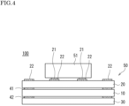
- FIG. 4 is a schematic configuration diagram schematically illustrating a configuration of a crystal oscillator (a crystal resonator and an oscillation IC) of the core section of FIG. 3 .
- FIG. 5 is a schematic plan view illustrating a first main surface of a first sealing member of the crystal oscillator of FIG. 4 .
- FIG. 6 is a schematic configuration diagram illustrating a variation of the crystal oscillator included in the core section of FIG. 2 .
- FIG. 7 is a cross-sectional view illustrating a schematic configuration of the OCXO according to a variation.
- FIGS. 8 ( a ) to 8 ( c ) are plan views each illustrating an example of the core substrate.
- FIGS. 9 ( a ) and 9 ( b ) are plan views each illustrating a variation of the core substrate.
- FIG. 10 is a cross-sectional view illustrating a variation of the OCXO.
- FIG. 11 is a bottom view illustrating the OCXO of FIG. 10 .
- an OCXO 1 has a configuration in which a core section 5 is disposed in a package (case) 2 made of ceramic or the like and having a substantially rectangular parallelepiped shape such that the core section 5 is hermetically sealed by a lid 3 .
- the package 2 includes a recess part 2 a whose upper part is opened, and the core section 5 is hermetically encapsulated in the recess part 2 a .
- the lid 3 is fixed by seam welding via a sealant 8 .
- the inside of the package 2 is hermetically sealed (in an airtight state).
- the sealant 8 a metal sealant such as Au-Su alloy and solder is suitably used, however, other sealants including low melting point glass may also be used.
- the sealing may be performed by seam welding with metal rings, direct seam welding without metal rings, or by beam welding. (However, note that the seam welding is preferred from the viewpoint of prevention of loss of vacuum).
- the space inside the package 2 is preferably in a vacuum state (for example, with the degree of vacuum not more than 10 Pa) or an atmosphere with low thermal conductivity with low pressure nitrogen or low pressure argon.
- FIG. 2 shows the OCXO 1 in the state in which the lid 3 is removed in order to indicate the internal configuration of the OCXO 1 .
- Step parts 2 c are formed on the inner wall surface of the peripheral wall part 2 b of the package 2 so as to be along the arrangement of connection terminals (not shown).
- the core section 5 is disposed on the bottom surface of the recess part 2 a between the facing pair of step parts 2 c and 2 c , via a core substrate (flexible substrate) 4 made of a flexible material having a plate shape.
- the step parts 2 c may be formed to surround the four sides of the bottom surface of the recess part 2 a .
- the core substrate 4 is bonded to the bottom surface of the recess part 2 a by a non-conductive adhesive (bonding material) 7 .
- a space (gap) 2 d is formed under the core substrate 4 .
- external terminals (not shown) formed on the respective components of the core section 5 are connected to the connection terminals formed on the step surfaces of the step parts 2 c by wire bonding via wires 6 a and 6 b .
- spacer members 2 f and 2 f are provided on the respective inner sides of the non-conductive adhesives 7 and 7 .
- the non-conductive adhesives 7 and 7 are disposed on both end parts of the core substrate 4 in the long-side direction so as to be straight lines extending in the short-side direction of the core substrate 4 (i.e. in the direction orthogonally intersecting the direction of the sheet on which FIG. 1 is illustrated).
- Each spacer member 2 f is located side by side with the corresponding non-conductive adhesive 7 so as to be a straight line extending in the short-side direction of the core substrate 4 .
- the respective spacer members 2 f and 2 f are interposed, each inside the corresponding non-conductive adhesive 7 , between the core substrate 4 and the bottom surface of the package 2 . Both end parts of the core substrate 4 in the long-side direction are supported by the respective spacer members 2 f and 2 f.
- the core substrate 4 is made of a resin material having heat resistance and flexibility such as polyimide.
- the spacer member 2 f is made of a paste material such as molybdenum and tungsten.
- the core substrate 4 is disposed so as not to come in contact with the bottom surface of the package 2 .
- the thickness of the core substrate 4 is preferably 5 to 100 ⁇ m.
- the width (distance) of the space 2 d between the core substrate 4 and the bottom surface of the package 2 is preferably 5 to 50 ⁇ m.
- a bonding region A 1 for bonding the core substrate 4 to the package 2 (i.e. a region A 1 onto which the non-conductive adhesive 7 is applied) is not superimposed, in plan view, on a region on the front surface of the core substrate 4 , on which the core section 5 is located.
- the core section 5 is disposed inside the respective pair of spacer members 2 f and 2 f in plan view, and the respective bonding regions A 1 and A 1 are disposed each outside the corresponding one of the pair of spacer members 2 f and 2 f .
- the distance from a heater IC 52 on the core substrate 4 to the bonding regions A 1 is preferably 250 to 1000 ⁇ m.
- FIG. 3 shows the core section 5 mounted on the core substrate 4 .
- the core section 5 packages various electronic components used for the OCXO 1 , and has a three-layer structure (layered structure) in which an oscillation IC 51 , a crystal resonator (piezoelectric resonator) 50 and the heater IC 52 are laminated in this order from the uppermost layer side. Respective areas in plan view of the oscillation IC 51 , the crystal resonator 50 and the heater IC 52 become gradually smaller from the downside to the upside.
- the core section 5 stabilizes oscillation frequency of the OCXO 1 by especially adjusting the temperatures of the crystal resonator 50 , the oscillation IC 51 and the heater IC 52 , whose temperature characteristics are large.
- the electronic components of the core section 5 are not sealed by a sealing resin, however, depending on the sealing atmosphere, the electronic components may be sealed by the sealing resin.
- a crystal oscillator 100 is constituted of the crystal resonator 50 and the oscillation IC 51 .
- the oscillation IC 51 is mounted on the crystal resonator 50 via a plurality of metal bumps.
- the oscillation frequency of the OCXO 1 is controlled by controlling the piezoelectric vibration of the crystal resonator 50 by the oscillation IC 51 .
- the crystal oscillator 100 will be described later in detail.
- a non-conductive adhesive 53 is interposed, which fixes the respective facing surfaces of the crystal resonator 50 and the oscillation IC 51 to each other.
- the front surface of the crystal resonator 50 i.e. a first main surface 201 of a first sealing member 20
- the rear surface of the oscillation IC 51 via the non-conductive adhesive 53 .
- the oscillation IC 51 has the area smaller than the area of the crystal resonator 50 in plan view. Thus, the whole oscillation IC 51 is disposed within the area of the crystal resonator 50 in plan view. Also, the whole rear surface of the oscillation IC 51 is bonded to the front surface of the crystal resonator 50 (i.e. the first main surface 201 of the first sealing member 20 ).
- the heater IC 52 has a configuration in which a heating element (a heat source), a control circuit for controlling the temperature of the heating element (a current control circuit) and a temperature sensor for detecting the temperature of the heating element are integrally formed.
- a heating element a heat source
- a control circuit for controlling the temperature of the heating element a current control circuit
- a temperature sensor for detecting the temperature of the heating element are integrally formed.
- a non-conductive adhesive 54 is interposed, which fixes the respective facing surfaces of the crystal resonator 50 and the heater IC 52 to each other.
- the rear surface of the crystal resonator 50 i.e. a second main surface of a second sealing member 30
- the non-conductive adhesive 54 is bonded to the front surface of the heater IC 52 via the non-conductive adhesive 54 .
- the crystal resonator 50 has the area smaller than the area of the heater IC 52 in plan view. Thus, the whole crystal resonator 50 is disposed within the area of the heater IC 52 in plan view. Also, the whole rear surface of the crystal resonator 50 (i.e. the second main surface of the second sealing member) is bonded to the front surface of the heater IC 52 .
- a non-conductive adhesive 55 is interposed, which fixes the respective facing surfaces of the heater IC 52 and the core substrate 4 to each other.
- a polyimide adhesive or an epoxy adhesive is, for example, used.
- the external terminals for wire bonding are formed on the front surfaces of the crystal resonator 50 and the heater IC 52 .
- the wire bonding of the crystal resonator 50 as well as the wire bonding of the heater IC 52 are not performed before mounting the core section 5 on the package 2 , but are performed after mounting the core section 5 on the package 2 . That is, as shown in FIG. 1 , after the core section 5 is mounted on the package 2 , the external terminals formed on the front surface of the crystal resonator 50 are connected to the connection terminals formed on the step surfaces of the step parts 2 c via the wires 6 a .
- the external terminals formed on the front surface of the heater IC 52 are connected to the connection terminals formed on the step surfaces of the step parts 2 c via the wires 6 b . In this way, it is possible to perform wire bonding efficiently by performing it after mounting the core section 5 on the package 2 , which contributes to excellent productivity of the OCXO 1 .
- the kind of the crystal resonator 50 used for the core section 5 is not particularly limited, a device having a sandwich structure is suitably used, which serves to make the device thinner.
- the device having the sandwich structure is constituted of: the first sealing member and the second sealing member both made of glass or crystal; and a piezoelectric resonator plate made of, for example, crystal.
- the piezoelectric resonator plate includes a vibrating part, on respective main surfaces of which excitation electrodes are formed.
- the first sealing member and the second sealing member are laminated and bonded via the piezoelectric resonator plate.
- the vibrating part of the piezoelectric resonator plate is hermetically sealed in an internal space of this three-layer structured device.
- the crystal oscillator 100 integrally formed by the sandwich-structured crystal resonator 50 and the oscillation IC 51 is exemplarily described referring to FIGS. 4 and 5 . Since the sandwich-structured crystal resonator is publicly known, the detail description of the inner structure of the crystal resonator 50 is omitted here.
- the crystal oscillator 100 includes: a crystal resonator plate (piezoelectric resonator plate) 10 ; the first sealing member 20 ; the second sealing member 30 ; and the oscillation IC 51 .
- the crystal resonator plate 10 is bonded to the first sealing member 20 by an annular-shaped seal bonding part 41
- the crystal resonator plate 10 is bonded to the second sealing member 30 by an annular-shaped seal bonding part 42 .
- the package having a sandwich structure is formed so as to have a substantially rectangular parallelepiped shape.
- the seal bonding parts 41 and 42 are respectively formed, for example, by the following procedures: forming respectively bonding patterns having a surface of an Au layer (for example, a bonding pattern formed by a Ti layer and an Au layer in this order from the lowermost layer side) on respective bonding surfaces of the crystal resonator plate 10 , the first sealing member 20 and the second sealing member 30 ; and performing Au—Au diffusion bonding by bonding the respective bonding surfaces.
- the gap size between the crystal resonator plate 10 and the respective sealing members 20 and 30 can be minimized to approximately 0.15 to 1 ⁇ m, which is beneficial to make the core section 5 thin and also to reduce the heat capacity of the core section 5 .
- an internal space (cavity) inside the package is formed by bonding the first sealing member 20 and the second sealing member 30 respectively to the main surfaces of the crystal resonator plate 10 , where the vibrating part is formed.
- the vibrating part of the crystal resonator plate 10 is hermetically sealed in the internal space.
- the oscillation IC 51 mounted on the first sealing member 20 is a one-chip integrated circuit element constituting, with the crystal resonator plate 10 , an oscillation circuit.
- the oscillation IC 51 is mounted on the crystal resonator 50 via a plurality of metal bumps 21 (i.e. by flip chip bonding).
- the present invention is not limited thereto.
- the oscillation IC 51 may be mounted on the crystal resonator 50 by die bonding, and may be electrically connected to the crystal resonator 50 by wire bonding.
- a solid electrode 43 may be formed, to which GND potential is applied when the OCXO 1 operates.
- the contact area between the oscillation IC 51 and the crystal resonator 50 is large compared to the configuration using the flip chip bonding, which leads to easy transfer of effect of heat generated in the oscillation IC 51 to the heater IC 52 that controls the temperature, via the crystal resonator 50 . Therefore, the temperature of the core section 5 (i.e. the temperature of the oscillation IC 51 , the crystal resonator 50 and the heater IC 52 ) can be efficiently transmitted to a temperature sensor that is provided in the heater IC 52 , which results in accurate temperature control.
- the crystal resonator 50 is not affected by the oscillation IC 51 that is a heat source other than the heater. However, it is actually difficult to avoid the heat effect by the oscillation IC 51 . In this case, it is possible to easily control the temperature by efficiently transmitting the temperature change of the crystal resonator 50 caused by the oscillation IC 51 to the temperature sensor of the heater IC 52 .
- the crystal resonator 50 is not directly connected to the package 2 by wire and only the oscillation IC 51 is directly connected to the crystal resonator 50 by wire, as shown in FIG. 7 .
- the crystal resonator 50 is connected, by wires 6 c , to only the oscillation IC 51 .
- external terminals 22 are formed on the front surface of the crystal resonator 50 .
- One end (outer side peripheral end) of each of two of the external terminals 22 is electrically connected to the excitation electrode of the vibrating part (via wirings and through holes in the crystal resonator 50 ), and the other end (inner side peripheral end) of each of these two external terminals 22 is connected to the oscillation IC 51 .
- one end (outer side peripheral end) of each of the remaining four external terminals 22 i.e. the external terminals 22 formed on the four corners
- is used for wire bonding to the package 2 and the other end (inner side peripheral end) of these remaining external terminals 22 is connected to the oscillation IC 51 .
- the oscillation IC 51 is connected to the external terminals 22 by the flip chip bonding (FCB) method using metal bumps.
- the core section 5 is hermetically encapsulated inside the thermal insulation package 2 .
- the core section 5 is mounted on the flexible core substrate 4 .
- the core substrate 4 is mechanically connected to the package 2 by the non-conductive adhesive 7 while the core section 5 and package 2 are electrically connected to each other by wire bonding.
- the space 2 d is provided between the core substrate and the bottom surface of the package 2 .
- the mechanical connection of core substrate 4 to the package 2 by the non-conductive adhesive 7 is separated from the electrical connection between the core section 5 and the package 2 by wire bonding, in order to obtain high reliability in both kinds of connections.
- the non-conductive adhesive 7 to connect the core substrate 4 to the package 2 , a flexible adhesive whose mechanical connection strength is not likely to decrease even when it is affected by external stress.
- the wire bonding between the core section 5 and the package 2 the common impedance noise is not likely to be generated by using the metal wires having a low electrical resistance, which leads to improvement of the carrier noise (CN) characteristics of the OCXO 1 .
- the heat capacity of the core section 5 can be reduced.
- the heat capacity of the core section 5 it is possible to control the temperature with low electric power, and furthermore, it is possible to improve the stability of the OCXO 1 by improving the temperature followability of the core section 5 .
- the heat capacity of the OCXO 1 is reduced, the OCXO 1 is likely to be affected by changes in the outside temperature.
- interposing the core substrate 4 between the core section and the package 2 it is possible to reduce stress as well as heat escape.
- the core section 5 is connected to the core substrate 4 on the front surface of the core substrate 4 while the core substrate 4 is connected to the package 2 on the rear surface of the core substrate 4 .
- the crystal resonator 50 and the heater IC 52 of the core section 5 are directly connected to the connection terminals formed in the package 2 via the wires 6 a and 6 b .
- the core substrate 4 is not required to mediate the electrical connection between the core section 5 and the package 2 .
- the non-conductive adhesive can be used.
- the non-conductive adhesive it is possible to use a flexible one compared to the conductive adhesive.
- the non-conductive adhesive has a mechanical connection strength that is not likely to decrease even when it is affected by external stress.
- the electrical connection between the core section 5 and the package 2 the common impedance noise is not likely to be generated by using the metal wires having a low electrical resistance, which leads to improvement of the carrier noise (CN) characteristics of the OCXO 1 .
- the core substrate 4 is only required to support the core section 5 with respect to the package 2 .
- the material options for the core substrate 4 increase.
- the core substrate 4 it is preferable to use a material having excellent thermal insulation and heat resistance.
- a flexible substrate so as to reduce the influence of the external stress.
- the flexible substrate made of a resin material such as polyimide is adopted as the core substrate 4 .
- the thermal insulation of the core section 5 by connecting the core section 5 to the package 2 via the core substrate 4 and furthermore forming the space 2 d under the core substrate 4 . Also, by forming the pair of step parts 2 c and 2 c in the package 2 so as to form the connection terminals on the step parts 2 c , the connection terminals get close to an opening part of the package 2 , which contributes to easy wire bonding of the core section 5 to the package 2 .
- the spacer members 2 f are interposed between the core substrate 4 and the bottom surface of the package 2 , at both end parts of the core substrate 4 in the long-side direction.
- the spacer members 2 f are disposed respectively inside the bonding regions A 1 for bonding the core substrate 4 to the package 2 . That is, the positions of the spacer members 2 f are closer to the region on which the core section 5 is mounted than the positions of the bonding regions A 1 are.
- the thickness of the non-conductive adhesive 7 applied onto the bonding regions A 1 is defined by the spacer members 2 f , which results in easy definition of the width of the space 2 d between the core substrate 4 and the bottom surface of the package 2 .
- the thickness of the spacer members 2 f is preferably 5 to 50 ⁇ m.
- the thickness of the non-conductive adhesive 7 varies depending on the applied amount of the non-conductive adhesive 7 onto the bonding region A 1 , which causes variations in the width of the space 2 d between the core substrate 4 and the package 2 . Variations also occur in the distance from the heater IC 52 on the core substrate 4 to the non-conductive adhesive 7 applied onto the bonding region A 1 . As a result, it will be difficult to stably perform the wire bonding of the crystal resonator 50 and the wire bonding of the heater IC 52 .
- the thickness of the non-conductive adhesive 7 applied onto the bonding region A 1 is defined by the spacer member 2 f .
- the spacer member 2 f it is possible to reduce the variation in the width of the space 2 d between the core substrate 4 and the bottom surface of the package 2 .
- the core substrate 4 is made of polyimide.
- the thickness of the core substrate 4 is set to 5 to 100 ⁇ m.
- the width of the space 2 d between the core substrate 4 and the bottom surface of the package 2 is set to 5 to 50 ⁇ m.
- the distance from the heater IC 52 on the core substrate 4 to the non-conductive adhesive 7 applied onto the bonding region A 1 is set to 250 to 1000 ⁇ m.
- the core substrate 4 bends too much at the time of the wire bonding, which causes difficulty in stable wire bonding.
- the crystal oscillator 100 including the sandwich-structured crystal resonator 50 is used.
- the present invention is not limited thereto.
- An oscillator having a structure other than the sandwich structure for example, a surface mount device (SMD) oscillator may be used.
- SMD surface mount device
- the number of the heaters included in the OCXO 1 is not particularly limited.
- the OCXO 1 may have a heater other than the heater included in the heater IC 52 .
- Examples of this configuration include: a configuration in which a heater is further added onto the core section 5 ; a configuration in which a heater is added to a mounting region for a circuit component, the region provided in the package 2 on a place other than the region for the core section 5 ; and a configuration in which a film-shaped heater is embedded in a main body of the package 2 .
- the heat dissipation from the core section 5 to the package 2 is generated mainly by heat transfer via the core substrate 4 .
- the heat transfer amount from the core section 5 to the package 2 can be decreased.
- FIG. 8 are plan views each illustrating an example of the core substrate 4 according to embodiment 2.
- a region R 1 for mounting the heater IC 52 as a part of the core section 5 thereon is located on the front surface of the core substrate 4 .
- a region R 2 to be bonded to the package 2 is located on the rear surface of the core substrate 4 .
- slits 401 are disposed between the region R 1 and the region R 2 .
- a heat transfer path between the region R 1 and the region R 2 becomes narrower due to the slits 401 .
- the slits 401 are arranged along its longitudinal direction (up-down direction in FIG. 8 ) that orthogonally intersects the arrangement direction (left-right direction in FIG. 8 ) of the regions R 2 arranged on both sides of the core substrate 4 .
- the slits 401 can prevent the heat from being transferred from the region R 1 to the regions R 2 over a wide range, which leads to improvement of thermal insulation by the slits 401 .
- the size of the slit 401 in its lateral direction does not particularly affect the thermal insulation of the slit 401 , it is preferably made as small as possible from the viewpoint of avoiding decrease in strength of the core substrate 4 .
- the strength of the core substrate 4 decreases, ultrasound does not efficiently contribute to wire bonding of the core section 5 to the package 2 , which prevents good wire bonding.
- the slit 401 disposed between the region R 1 and one region R 2 it is more preferable to make a plurality of slits divided in the longitudinal direction than to make one long slit (see FIG. 8 ( a ) ).
- a plurality of divided slits 401 can avoid decrease in strength of the core substrate 4 compared to the case in which one long slit is made.
- the shape of the slit 401 is not limited to a straight line shape.
- the slit 401 may be bent along the circumference of the region R 2 (see FIG. 8 ( b ) ). Like this, by bending the slit 401 along the surrounding shape of the region R 2 , it is possible to effectively block the heat transfer to the region R 2 . Thus, effective thermal insulation can be obtained by the slit 401 .
- the slit 401 is not limited to be located adjacent to the region R 2 between the region R 1 and the region R 2 .
- the slit 401 may be disposed adjacent to the region R 1 (see FIG. 8 ( c ) ).
- the slit 401 by disposing the slit 401 adjacent to the region R 1 , it is possible to efficiently block the heat transfer from the region R 1 (i.e. heat transfer from the heater IC 52 as the heat source), that is, it is possible to efficiently block the heat transfer in the vicinity of the heat source of the heat to be radiantly transferred via the region R 1 .
- effective thermal insulation can be obtained by the slit 401 .
- FIG. 9 are plan views each illustrating an example of the core substrate 4 according to embodiment 3.
- an opening 402 is provided in a region directly under the heater IC 52 that is a part of the core section 5 so as to almost superimpose on the region R 1 . Thanks to the opening 402 , the contact area between the heater IC 52 and the core substrate 4 is reduced, which leads to decrease of the heat transfer amount from the heater IC 52 to the core substrate 4 . As a result, it is possible to reduce the heat dissipation from the core section 5 to the package 2 caused by the heat transfer via the core substrate 4 .
- the opening 402 does not completely include the region R 1 inside the opening.
- the opening 402 has a shape that does not include at least four corners of the region R 1 . In this way, the heater IC 52 can be bonded and fixed to the core substrate 4 at the four corners thereof.
- the opening 402 shown in FIG. 9 ( a ) is formed so as to have the vertical size and the horizontal size both larger than the vertical size and the horizontal size of the region R 1 .
- the region R 1 has a shape in which only the four corners thereof are not included in the opening 402 . In this case, it is possible to minimize the contact area between the heater IC 52 and the core substrate 4 , and thus to maximally obtain the heat transfer reduction effect (thermal insulation) by the opening 402 .
- the opening 402 shown in FIG. 9 ( b ) is formed so as to have the vertical size and the horizontal size both smaller than the vertical size and the horizontal size of the region R 1 .
- the region R 1 has a shape in which not only the four corners thereof but also whole the vicinity of the outer edge thereof are not included in the opening 402 .
- the opening 402 does not exist directly under the pads of the core section 5 for wire bonding when the core section 5 is bonded to the package 2 by wire bonding.
- the posture of the core section 5 can be stabilized when performing wire bonding and thus ultrasound can efficiently contribute to wire bonding, which leads to good wire bonding.
- the package 2 is a single package.
- the present invention is not limited thereto. It is possible to use, for example, an H-shaped package as shown in FIG. 10 , or a stacked configuration of two packages.
- the OCXO 1 with the H-shaped package has the package 2 that includes, apart from the recess part 2 a whose upper part is opened, a recess part 2 e whose lower part is opened.
- a circuit component a circuit component attached by a bonding material (for example, solder) for circuit component
- a capacitor 9 an electronic component for adjustment that is used in combination with the heater IC 52 .
- the recess part 2 e in which the capacitor 9 is disposed is not needed to be sealed by the lid 3 .
- the capacitor 9 can also be disposed in the package where the core section is housed (i.e. in the recess part 2 a ).
- three capacitors 9 are mounted on the second main surface that is opposite to the first main surface of the package 2 (in this case, mounted on the bottom surface of the recess part 2 e ).
- the capacitors 9 are bonded, by solder, to mounting pads 9 a (mounting pads for circuit component) that are formed on the bottom surface of the recess part 2 e of the package 2 .
- the locations of the capacitors 9 are shown by the dashed-dotted line.
- a pair of mounting pads 9 a and 9 a is arranged so as to face each other in the short-side direction of the package 2 . Both end parts of each of the three capacitors 9 in the short-side direction of the package 2 are bonded to the mounting pads 9 a and 9 a.
- three pairs of mounting pads 9 a and 9 a are arranged at predetermined intervals in the long-side direction of the package 2 .
- the mounting pads 9 a are located like islands on the bottom surface of the package 2 .
- the package 2 and the three capacitors 9 each have a rectangular shape in plan view, and the three capacitors 9 are arranged so as to be symmetrical with respect to a center line L 1 in the short-side direction of the package 2 and a center line L 2 in the long-side direction of the package 2 . In this case, it is sufficient that the locations of the three capacitors 9 are linearly symmetrical with respect to the center line L 1 and the center line L 2 .
- the number of the capacitors 9 mounted on the second surface of the package 2 is not particularly limited.
- the number of the capacitors 9 may be other than three.
- a circuit component other than the capacitor 9 may be mounted on the second surface of the package 2 .
- the size (volume and surface area) of each circuit component is not necessarily required to be the same.
- the three capacitors 9 are arranged so as to be linearly symmetrical with respect to both the center line L 1 and the center line L 2 .
- the three capacitors 9 may be linearly symmetrical with respect to at least one of the center lines L 1 and L 2 .
- the three capacitors 9 may be linearly symmetrical with respect to only the center line L 1 in the short-side direction of the package 2 .
- the three capacitors 9 may be linearly symmetrical with respect to only the center line L 2 in the long-side direction of the package 2 . In this way, it is possible to maintain symmetry in the heat transfer in a specific side direction of the package 2 , which prevents unevenness of the heat transfer. Thus, it is possible to stabilize the temperature control or the properties of the OCXO 1 .
- the second main surface opposite to the first main surface on which the recess part 2 a is formed may be a flat surface, and the capacitors 9 may be provided on this flat surface.
- the two packages each having a recess part on only one side may be laminated in the up-down direction and electrically and mechanically connected to each other so that the upper package is hermetically sealed by the lid (not shown).
- the core section 5 is housed in the recess part of the upper package as shown in FIG. 1 while only the capacitor is housed in the lower package.
- the above-described core section 5 has a three-layer structure in which the oscillation IC 51 , the crystal resonator 50 and the heater IC 52 are laminated in this order from the uppermost layer side.
- the oscillation IC 51 and the crystal resonator 50 may be horizontally placed (disposed side-by-side) on the heater IC 52 .
- the crystal resonator 50 is hardly affected by the heat from the oscillation IC 51 and thus the respective temperatures of the crystal resonator 50 and the heater IC 52 are easily homogenized.
Landscapes
- Piezo-Electric Or Mechanical Vibrators, Or Delay Or Filter Circuits (AREA)
- Oscillators With Electromechanical Resonators (AREA)
- Cooling Or The Like Of Semiconductors Or Solid State Devices (AREA)
Abstract
Description
-
- [Patent Document 1] JP 2012-205093 A
- [Patent Document 2] JP 2018-014705 A
-
- 1 OCXO (oven-controlled crystal oscillator)
- 2 Package
- 2 d Space
- 2 f Spacer member
- 4 Core substrate (flexible substrate)
- 5 Core section
- 7 Non-conductive adhesive (bonding material)
- 50 Crystal resonator (piezoelectric resonator)
- 51 Oscillation IC
- 52 Heater IC
Claims (8)
Applications Claiming Priority (3)
| Application Number | Priority Date | Filing Date | Title |
|---|---|---|---|
| JP2021-031583 | 2021-03-01 | ||
| JP2021031583 | 2021-03-01 | ||
| PCT/JP2022/008247 WO2022186124A1 (en) | 2021-03-01 | 2022-02-28 | Thermostatic bath-type piezoelectric oscillator |
Publications (3)
| Publication Number | Publication Date |
|---|---|
| US20240136976A1 US20240136976A1 (en) | 2024-04-25 |
| US20240235478A9 US20240235478A9 (en) | 2024-07-11 |
| US12283919B2 true US12283919B2 (en) | 2025-04-22 |
Family
ID=83153785
Family Applications (1)
| Application Number | Title | Priority Date | Filing Date |
|---|---|---|---|
| US18/278,424 Active US12283919B2 (en) | 2021-03-01 | 2022-02-28 | Oven-controlled crystal oscillator |
Country Status (5)
| Country | Link |
|---|---|
| US (1) | US12283919B2 (en) |
| JP (2) | JPWO2022186124A1 (en) |
| CN (1) | CN117063391A (en) |
| TW (1) | TW202245406A (en) |
| WO (1) | WO2022186124A1 (en) |
Citations (10)
| Publication number | Priority date | Publication date | Assignee | Title |
|---|---|---|---|---|
| JP2005039435A (en) | 2003-07-17 | 2005-02-10 | Toyo Commun Equip Co Ltd | Surface mount type piezoelectric oscillator |
| JP2012205093A (en) | 2011-03-25 | 2012-10-22 | Nippon Dempa Kogyo Co Ltd | Oscillator |
| US20170063379A1 (en) | 2015-08-28 | 2017-03-02 | Seiko Epson Corporation | Electronic device, method of manufacturing electronic device, electronic apparatus, and moving object |
| US20180013386A1 (en) | 2016-07-07 | 2018-01-11 | Nihon Dempa Kogyo Co., Ltd. | Oven-controlled crystal oscillator |
| US20180009195A1 (en) | 2015-01-13 | 2018-01-11 | Hitachi Chemical Company, Ltd. | Resin film for flexible printed circuit board, metal foil provided with resin, coverlay film, bonding sheet, and flexible printed circuit board |
| JP2018014705A (en) | 2016-07-07 | 2018-01-25 | 日本電波工業株式会社 | Thermostatic bath crystal oscillator |
| US20180337634A1 (en) | 2017-05-18 | 2018-11-22 | Seiko Epson Corporation | Oscillator and electronic apparatus |
| JP2018196105A (en) | 2017-05-18 | 2018-12-06 | セイコーエプソン株式会社 | Oscillator and electronic apparatus |
| JP2020120195A (en) | 2019-01-21 | 2020-08-06 | 株式会社大真空 | MEMS oscillator |
| US10812017B1 (en) * | 2019-08-02 | 2020-10-20 | Advanced Semiconductor Engineering, Inc. | Semiconductor package structure |
Family Cites Families (1)
| Publication number | Priority date | Publication date | Assignee | Title |
|---|---|---|---|---|
| JP2012134792A (en) * | 2010-12-22 | 2012-07-12 | Daishinku Corp | Surface mounted piezoelectric oscillator |
-
2022
- 2022-02-28 JP JP2023503813A patent/JPWO2022186124A1/ja active Pending
- 2022-02-28 WO PCT/JP2022/008247 patent/WO2022186124A1/en not_active Ceased
- 2022-02-28 US US18/278,424 patent/US12283919B2/en active Active
- 2022-02-28 CN CN202280015953.8A patent/CN117063391A/en active Pending
- 2022-03-01 TW TW111107362A patent/TW202245406A/en unknown
-
2025
- 2025-04-14 JP JP2025066365A patent/JP7761172B2/en active Active
Patent Citations (12)
| Publication number | Priority date | Publication date | Assignee | Title |
|---|---|---|---|---|
| JP2005039435A (en) | 2003-07-17 | 2005-02-10 | Toyo Commun Equip Co Ltd | Surface mount type piezoelectric oscillator |
| JP2012205093A (en) | 2011-03-25 | 2012-10-22 | Nippon Dempa Kogyo Co Ltd | Oscillator |
| US20180009195A1 (en) | 2015-01-13 | 2018-01-11 | Hitachi Chemical Company, Ltd. | Resin film for flexible printed circuit board, metal foil provided with resin, coverlay film, bonding sheet, and flexible printed circuit board |
| US20170063379A1 (en) | 2015-08-28 | 2017-03-02 | Seiko Epson Corporation | Electronic device, method of manufacturing electronic device, electronic apparatus, and moving object |
| JP2017046272A (en) | 2015-08-28 | 2017-03-02 | セイコーエプソン株式会社 | Electronic device, electronic device manufacturing method, electronic apparatus, and moving body |
| CN106487331A (en) | 2015-08-28 | 2017-03-08 | 精工爱普生株式会社 | Electronic device, the manufacture method of electronic device, electronic equipment and moving body |
| US20180013386A1 (en) | 2016-07-07 | 2018-01-11 | Nihon Dempa Kogyo Co., Ltd. | Oven-controlled crystal oscillator |
| JP2018014705A (en) | 2016-07-07 | 2018-01-25 | 日本電波工業株式会社 | Thermostatic bath crystal oscillator |
| US20180337634A1 (en) | 2017-05-18 | 2018-11-22 | Seiko Epson Corporation | Oscillator and electronic apparatus |
| JP2018196105A (en) | 2017-05-18 | 2018-12-06 | セイコーエプソン株式会社 | Oscillator and electronic apparatus |
| JP2020120195A (en) | 2019-01-21 | 2020-08-06 | 株式会社大真空 | MEMS oscillator |
| US10812017B1 (en) * | 2019-08-02 | 2020-10-20 | Advanced Semiconductor Engineering, Inc. | Semiconductor package structure |
Also Published As
| Publication number | Publication date |
|---|---|
| US20240136976A1 (en) | 2024-04-25 |
| JP7761172B2 (en) | 2025-10-28 |
| CN117063391A (en) | 2023-11-14 |
| JPWO2022186124A1 (en) | 2022-09-09 |
| US20240235478A9 (en) | 2024-07-11 |
| WO2022186124A1 (en) | 2022-09-09 |
| TW202245406A (en) | 2022-11-16 |
| JP2025103043A (en) | 2025-07-08 |
Similar Documents
| Publication | Publication Date | Title |
|---|---|---|
| US6229249B1 (en) | Surface-mount type crystal oscillator | |
| US12107543B2 (en) | Oven-controlled crystal oscillator | |
| US12531511B2 (en) | Oven-controlled crystal oscillator | |
| US12283919B2 (en) | Oven-controlled crystal oscillator | |
| US12249955B2 (en) | Oven-controlled crystal oscillator | |
| US12249956B2 (en) | Oven-controlled crystal oscillator | |
| US20240305269A1 (en) | Piezoelectric resonator device | |
| JP7420225B2 (en) | Constant temperature oven type piezoelectric oscillator | |
| JP7571637B2 (en) | Thermostatic oven type piezoelectric oscillator | |
| JP2023051073A (en) | Thermostatted Piezoelectric Oscillator | |
| JP2009239475A (en) | Surface mounting piezoelectric oscillator | |
| JP2024158291A (en) | Thermostatic oven type piezoelectric oscillator | |
| JP2024158290A (en) | Thermostatic oven type piezoelectric oscillator | |
| JP6538310B2 (en) | Piezoelectric device with thermostat | |
| WO2023182062A1 (en) | Thermostatic oven type piezoelectric oscillator | |
| JP2025027712A (en) | Thermostatic oven type piezoelectric oscillator | |
| WO2025164243A1 (en) | Oven-controlled crystal oscillator | |
| JP2025121592A (en) | Oven-type piezoelectric oscillator |
Legal Events
| Date | Code | Title | Description |
|---|---|---|---|
| AS | Assignment |
Owner name: DAISHINKU CORPORATION, JAPAN Free format text: ASSIGNMENT OF ASSIGNORS INTEREST;ASSIGNOR:KOJO, TAKUYA;REEL/FRAME:064673/0323 Effective date: 20230807 |
|
| FEPP | Fee payment procedure |
Free format text: ENTITY STATUS SET TO UNDISCOUNTED (ORIGINAL EVENT CODE: BIG.); ENTITY STATUS OF PATENT OWNER: LARGE ENTITY |
|
| STPP | Information on status: patent application and granting procedure in general |
Free format text: DOCKETED NEW CASE - READY FOR EXAMINATION |
|
| STPP | Information on status: patent application and granting procedure in general |
Free format text: NON FINAL ACTION MAILED |
|
| STPP | Information on status: patent application and granting procedure in general |
Free format text: RESPONSE TO NON-FINAL OFFICE ACTION ENTERED AND FORWARDED TO EXAMINER |
|
| STPP | Information on status: patent application and granting procedure in general |
Free format text: NOTICE OF ALLOWANCE MAILED -- APPLICATION RECEIVED IN OFFICE OF PUBLICATIONS |
|
| STPP | Information on status: patent application and granting procedure in general |
Free format text: NOTICE OF ALLOWANCE MAILED -- APPLICATION RECEIVED IN OFFICE OF PUBLICATIONS |
|
| STCF | Information on status: patent grant |
Free format text: PATENTED CASE |