US12267022B2 - Power conversion device, power conversion method, and program - Google Patents
Power conversion device, power conversion method, and program Download PDFInfo
- Publication number
- US12267022B2 US12267022B2 US17/757,865 US202017757865A US12267022B2 US 12267022 B2 US12267022 B2 US 12267022B2 US 202017757865 A US202017757865 A US 202017757865A US 12267022 B2 US12267022 B2 US 12267022B2
- Authority
- US
- United States
- Prior art keywords
- frequency
- current
- secondary side
- carrier wave
- band
- Prior art date
- Legal status (The legal status is an assumption and is not a legal conclusion. Google has not performed a legal analysis and makes no representation as to the accuracy of the status listed.)
- Active, expires
Links
Images


Classifications
-
- H—ELECTRICITY
- H02—GENERATION; CONVERSION OR DISTRIBUTION OF ELECTRIC POWER
- H02M—APPARATUS FOR CONVERSION BETWEEN AC AND AC, BETWEEN AC AND DC, OR BETWEEN DC AND DC, AND FOR USE WITH MAINS OR SIMILAR POWER SUPPLY SYSTEMS; CONVERSION OF DC OR AC INPUT POWER INTO SURGE OUTPUT POWER; CONTROL OR REGULATION THEREOF
- H02M5/00—Conversion of AC power input into AC power output, e.g. for change of voltage, for change of frequency, for change of number of phases
- H02M5/02—Conversion of AC power input into AC power output, e.g. for change of voltage, for change of frequency, for change of number of phases without intermediate conversion into DC
- H02M5/04—Conversion of AC power input into AC power output, e.g. for change of voltage, for change of frequency, for change of number of phases without intermediate conversion into DC by static converters
- H02M5/22—Conversion of AC power input into AC power output, e.g. for change of voltage, for change of frequency, for change of number of phases without intermediate conversion into DC by static converters using discharge tubes with control electrode or semiconductor devices with control electrode
- H02M5/275—Conversion of AC power input into AC power output, e.g. for change of voltage, for change of frequency, for change of number of phases without intermediate conversion into DC by static converters using discharge tubes with control electrode or semiconductor devices with control electrode using devices of a triode or transistor type requiring continuous application of a control signal
- H02M5/293—Conversion of AC power input into AC power output, e.g. for change of voltage, for change of frequency, for change of number of phases without intermediate conversion into DC by static converters using discharge tubes with control electrode or semiconductor devices with control electrode using devices of a triode or transistor type requiring continuous application of a control signal using semiconductor devices only
- H02M5/2932—Conversion of AC power input into AC power output, e.g. for change of voltage, for change of frequency, for change of number of phases without intermediate conversion into DC by static converters using discharge tubes with control electrode or semiconductor devices with control electrode using devices of a triode or transistor type requiring continuous application of a control signal using semiconductor devices only with automatic control of output voltage, current or power
- H02M5/2935—Conversion of AC power input into AC power output, e.g. for change of voltage, for change of frequency, for change of number of phases without intermediate conversion into DC by static converters using discharge tubes with control electrode or semiconductor devices with control electrode using devices of a triode or transistor type requiring continuous application of a control signal using semiconductor devices only with automatic control of output voltage, current or power using reverse phase control, i.e. turn-on of switches in series with load at zero crossing of input voltage, turn-off before next zero crossing
-
- H—ELECTRICITY
- H02—GENERATION; CONVERSION OR DISTRIBUTION OF ELECTRIC POWER
- H02M—APPARATUS FOR CONVERSION BETWEEN AC AND AC, BETWEEN AC AND DC, OR BETWEEN DC AND DC, AND FOR USE WITH MAINS OR SIMILAR POWER SUPPLY SYSTEMS; CONVERSION OF DC OR AC INPUT POWER INTO SURGE OUTPUT POWER; CONTROL OR REGULATION THEREOF
- H02M1/00—Details of apparatus for conversion
- H02M1/0048—Circuits or arrangements for reducing losses
- H02M1/0054—Transistor switching losses
- H02M1/0058—Transistor switching losses by employing soft switching techniques, i.e. commutation of transistors when applied voltage is zero or when current flow is zero
-
- H—ELECTRICITY
- H02—GENERATION; CONVERSION OR DISTRIBUTION OF ELECTRIC POWER
- H02M—APPARATUS FOR CONVERSION BETWEEN AC AND AC, BETWEEN AC AND DC, OR BETWEEN DC AND DC, AND FOR USE WITH MAINS OR SIMILAR POWER SUPPLY SYSTEMS; CONVERSION OF DC OR AC INPUT POWER INTO SURGE OUTPUT POWER; CONTROL OR REGULATION THEREOF
- H02M5/00—Conversion of AC power input into AC power output, e.g. for change of voltage, for change of frequency, for change of number of phases
- H02M5/02—Conversion of AC power input into AC power output, e.g. for change of voltage, for change of frequency, for change of number of phases without intermediate conversion into DC
- H02M5/04—Conversion of AC power input into AC power output, e.g. for change of voltage, for change of frequency, for change of number of phases without intermediate conversion into DC by static converters
- H02M5/22—Conversion of AC power input into AC power output, e.g. for change of voltage, for change of frequency, for change of number of phases without intermediate conversion into DC by static converters using discharge tubes with control electrode or semiconductor devices with control electrode
- H02M5/275—Conversion of AC power input into AC power output, e.g. for change of voltage, for change of frequency, for change of number of phases without intermediate conversion into DC by static converters using discharge tubes with control electrode or semiconductor devices with control electrode using devices of a triode or transistor type requiring continuous application of a control signal
- H02M5/293—Conversion of AC power input into AC power output, e.g. for change of voltage, for change of frequency, for change of number of phases without intermediate conversion into DC by static converters using discharge tubes with control electrode or semiconductor devices with control electrode using devices of a triode or transistor type requiring continuous application of a control signal using semiconductor devices only
-
- H—ELECTRICITY
- H02—GENERATION; CONVERSION OR DISTRIBUTION OF ELECTRIC POWER
- H02M—APPARATUS FOR CONVERSION BETWEEN AC AND AC, BETWEEN AC AND DC, OR BETWEEN DC AND DC, AND FOR USE WITH MAINS OR SIMILAR POWER SUPPLY SYSTEMS; CONVERSION OF DC OR AC INPUT POWER INTO SURGE OUTPUT POWER; CONTROL OR REGULATION THEREOF
- H02M5/00—Conversion of AC power input into AC power output, e.g. for change of voltage, for change of frequency, for change of number of phases
- H02M5/02—Conversion of AC power input into AC power output, e.g. for change of voltage, for change of frequency, for change of number of phases without intermediate conversion into DC
- H02M5/04—Conversion of AC power input into AC power output, e.g. for change of voltage, for change of frequency, for change of number of phases without intermediate conversion into DC by static converters
- H02M5/22—Conversion of AC power input into AC power output, e.g. for change of voltage, for change of frequency, for change of number of phases without intermediate conversion into DC by static converters using discharge tubes with control electrode or semiconductor devices with control electrode
- H02M5/275—Conversion of AC power input into AC power output, e.g. for change of voltage, for change of frequency, for change of number of phases without intermediate conversion into DC by static converters using discharge tubes with control electrode or semiconductor devices with control electrode using devices of a triode or transistor type requiring continuous application of a control signal
- H02M5/297—Conversion of AC power input into AC power output, e.g. for change of voltage, for change of frequency, for change of number of phases without intermediate conversion into DC by static converters using discharge tubes with control electrode or semiconductor devices with control electrode using devices of a triode or transistor type requiring continuous application of a control signal for conversion of frequency
-
- H—ELECTRICITY
- H02—GENERATION; CONVERSION OR DISTRIBUTION OF ELECTRIC POWER
- H02P—CONTROL OR REGULATION OF ELECTRIC MOTORS, ELECTRIC GENERATORS OR DYNAMO-ELECTRIC CONVERTERS; CONTROLLING TRANSFORMERS, REACTORS OR CHOKE COILS
- H02P27/00—Arrangements or methods for the control of AC motors characterised by the kind of supply voltage
- H02P27/04—Arrangements or methods for the control of AC motors characterised by the kind of supply voltage using variable-frequency supply voltage, e.g. inverter or converter supply voltage
- H02P27/06—Arrangements or methods for the control of AC motors characterised by the kind of supply voltage using variable-frequency supply voltage, e.g. inverter or converter supply voltage using DC to AC converters or inverters
- H02P27/08—Arrangements or methods for the control of AC motors characterised by the kind of supply voltage using variable-frequency supply voltage, e.g. inverter or converter supply voltage using DC to AC converters or inverters with pulse width modulation
- H02P27/085—Arrangements or methods for the control of AC motors characterised by the kind of supply voltage using variable-frequency supply voltage, e.g. inverter or converter supply voltage using DC to AC converters or inverters with pulse width modulation wherein the PWM mode is adapted on the running conditions of the motor, e.g. the switching frequency
-
- H—ELECTRICITY
- H02—GENERATION; CONVERSION OR DISTRIBUTION OF ELECTRIC POWER
- H02P—CONTROL OR REGULATION OF ELECTRIC MOTORS, ELECTRIC GENERATORS OR DYNAMO-ELECTRIC CONVERTERS; CONTROLLING TRANSFORMERS, REACTORS OR CHOKE COILS
- H02P27/00—Arrangements or methods for the control of AC motors characterised by the kind of supply voltage
- H02P27/04—Arrangements or methods for the control of AC motors characterised by the kind of supply voltage using variable-frequency supply voltage, e.g. inverter or converter supply voltage
- H02P27/16—Arrangements or methods for the control of AC motors characterised by the kind of supply voltage using variable-frequency supply voltage, e.g. inverter or converter supply voltage using AC to AC converters without intermediate conversion to DC
-
- H—ELECTRICITY
- H02—GENERATION; CONVERSION OR DISTRIBUTION OF ELECTRIC POWER
- H02M—APPARATUS FOR CONVERSION BETWEEN AC AND AC, BETWEEN AC AND DC, OR BETWEEN DC AND DC, AND FOR USE WITH MAINS OR SIMILAR POWER SUPPLY SYSTEMS; CONVERSION OF DC OR AC INPUT POWER INTO SURGE OUTPUT POWER; CONTROL OR REGULATION THEREOF
- H02M1/00—Details of apparatus for conversion
- H02M1/0003—Details of control, feedback or regulation circuits
Definitions
- the present disclosure relates to a power conversion device, a power conversion method, and a program.
- Patent Document 1 discloses a matrix converter including a plurality of bidirectional switches connecting phases of an alternating current power source and phases of an alternating current device.
- the matrix converter outputs electric power generated in the alternating current device to the alternating current power source and controls the alternating current device based on electric power supplied from the alternating current power source.
- FIG. 8 is a flowchart illustrating an example of the setting procedure of the frequency of the carrier wave according to FIG. 4 .
- FIG. 11 is a flowchart illustrating an example of a setting procedure of the frequency of the carrier wave according to FIG. 10 .
- FIG. 12 is a flowchart illustrating an example of the setting procedure of the frequency of the carrier wave according to FIG. 10 .
- FIG. 13 is a flowchart illustrating an example of the setting procedure of the frequency of the carrier wave according to FIG. 10 .
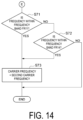
- FIG. 14 is a flowchart illustrating an example of the setting procedure of the frequency of the carrier wave according to FIG. 10 .
- a power conversion device 1 illustrated in FIG. 1 is a device that performs bidirectional power conversion between alternating current power on a primary side and alternating current power on a secondary side.
- the power conversion device 1 converts the alternating current power on the primary side supplied from a power source 91 into the alternating current power on the secondary side and supplies the alternating current power on the secondary side to an electric motor 92 .
- the power conversion device 1 converts the alternating current power on the secondary side generated by the electric motor 92 (regenerative power) into the alternating current power on the primary side and supplies the alternating current power on the primary side to the power source 91 .
- the power conversion device 1 includes a matrix converter circuit 10 , a filter 30 , a voltage detection circuit 40 , a current sensor 50 , and a control circuit 100 .
- the matrix converter circuit 10 includes a plurality of switching elements, and performs bidirectional power conversion between the alternating current power on the primary side and the alternating current power on the secondary side. In this bidirectional power conversion, conversion into a direct current is not involved.
- the matrix converter circuit 10 includes power lines on the primary side 11 R, 11 S, and 11 T, the power lines on the secondary side 12 U, 12 V, and 12 W, and nine bidirectional switches 2 RU, 2 SU, 2 TU, 2 RV, 2 SV, 2 TV, 2 RW, 2 SW, and 2 TW.
- the power line 11 R is a transmission line for the R phase
- the power line 115 is a transmission line for the S phase
- the power line 11 T is a transmission line for the T phase.
- the power line 12 U is a transmission line for the U phase
- the power line 12 V is a transmission line for the V phase
- the power line 12 W is a transmission line for the W phase.
- Each of the bidirectional switches 2 RU, 2 SU, 2 TU, 2 RV, 2 SV, 2 TV, 2 RW, 2 SW, and 2 TW switches among three states, which are a state in which the switch allows a current to flow from the primary side to the secondary side, a state in which the switch allows a current to flow from the secondary side to the primary side, and a state in which the switch does not allow a current to flow.
- the bidirectional switch 2 RU is interposed between the power line 11 R and the power line 12 U, and switches among a first ON state in which the bidirectional switch 2 RU allows a current to flow from the power line 11 R to the power line 12 U, a second ON state in which the bidirectional switch 2 RU allows a current to flow from the power line 12 U to the power line 11 R, and a bidirectional OFF state in which the bidirectional switch 2 RU does not allow a current to flow.
- the bidirectional switch 2 SU is interposed between the power line 115 and the power line 12 U, and switches among a first ON state in which the bidirectional switch 2 SU allows a current to flow from the power line 115 to the power line 12 U, a second ON state in which the bidirectional switch 2 SU allows a current to flow from the power line 12 U to the power line 11 S, and a bidirectional OFF state in which the bidirectional switch 2 SU does not allow a current to flow.
- the bidirectional switch 2 TU is interposed between the power line 11 T and the power line 12 U, and switches among a first ON state in which the bidirectional switch 2 TU allows a current to flow from the power line 11 T to the power line 12 U, a second ON state in which the bidirectional switch 2 TU allows a current to flow from the power line 12 U to the power line 11 T, and a bidirectional OFF state in which the bidirectional switch 2 TU does not allow a current to flow.
- the bidirectional switch 2 RV is interposed between the power line 11 R and the power line 12 V, and switches among a first ON state in which the bidirectional switch 2 RV allows a current to flow from the power line 11 R to the power line 12 V, a second ON state in which the bidirectional switch 2 RV allows a current to flow from the power line 12 V to the power line 11 R, and a bidirectional OFF state in which the bidirectional switch 2 RV does not allow a current to flow.
- the bidirectional switch 2 SV is interposed between the power line 11 S and the power line 12 V, and switches among a first ON state in which the bidirectional switch 2 SV allows a current to flow from the power line 11 S to the power line 12 V, a second ON state in which the bidirectional switch 2 SV allows a current to flow from the power line 12 V to the power line 11 S, and a bidirectional OFF state in which the bidirectional switch 2 SV does not allow a current to flow.
- the bidirectional switch 2 TV is interposed between the power line 11 T and the power line 12 V, and switches among a first ON state in which the bidirectional switch 2 TV allows a current to flow from the power line 11 T to the power line 12 V, a second ON state in which the bidirectional switch 2 TV allows a current to flow from the power line 12 V to the power line 11 T, and a bidirectional OFF state in which the bidirectional switch 2 TV does not allow a current to flow.
- the bidirectional switch 2 RW is interposed between the power line 11 R and the power line 12 W, and switches among a first ON state in which the bidirectional switch 2 RW allows a current to flow from the power line 11 R to the power line 12 W, a second ON state in which the bidirectional switch 2 RW allows a current to flow from the power line 12 W to the power line 11 R, and a bidirectional OFF state in which the bidirectional switch 2 RW does not allow a current to flow.
- the bidirectional switch 2 SW is interposed between the power line 11 S and the power line 12 W, and switches among a first ON state in which the bidirectional switch 2 SW allows a current to flow from the power line 11 S to the power line 12 W, a second ON state in which the bidirectional switch 2 SW allows a current to flow from the power line 12 W to the power line 11 S, and a bidirectional OFF state in which the bidirectional switch 2 SW does not allow a current to flow.
- the bidirectional switch 2 TW is interposed between the power line 11 T and the power line 12 W, and switches among a first ON state in which the bidirectional switch 2 TW allows a current to flow from the power line 11 T to the power line 12 W, a second ON state in which the bidirectional switch 2 TW allows a current to flow from the power line 12 W to the power line 11 T, and a bidirectional OFF state in which the bidirectional switch 2 TW does not allow a current to flow.
- each of the bidirectional switches 2 RU, 2 SU, 2 TU, 2 RV, 2 SV, 2 TV, 2 RW, 2 SW, and 2 TW has two switches 21 and 22 .
- the switch 21 in an ON state allows a current to flow from the primary side to the secondary side and does not allow a current to flow from the secondary side to the primary side.
- the switch 22 in an ON state allows a current to flow from the secondary side to the primary side and does not allow a current to flow from the primary side to the secondary side.
- the filter 30 reduces harmonics in the alternating current power on the primary side.
- the filter 30 includes inductors 31 R, 31 S, and 31 T, and capacitors 34 R, 34 S, and 34 T.
- the inductors 31 R, 31 S, and 31 T are provided in the power lines 11 R, 11 S, and 11 T, respectively.
- the capacitor 34 R is provided on the secondary side of the inductor 31 R (between the inductor 31 R and the bidirectional switches 2 RU, 2 RV, and 2 RW) and between the power line 11 R and a neutral point 35 .
- the capacitor 34 S is provided on the secondary side of the inductor 31 S (between the inductor 31 S and the bidirectional switches 2 SU, 2 SV, and 2 SW) and between the power line 11 S and the neutral point 35 .
- the capacitor 34 T is provided on the secondary side of the inductor 31 T (between the inductor 31 T and the bidirectional switches 2 TU, 2 TV, and 2 TW) and between the power line 11 T and the neutral point 35 .
- the voltage detection circuit 40 detects an alternating current voltage on the primary side. For example, the voltage detection circuit 40 detects a phase voltage of each of the power lines 11 R, 11 S, and 11 T.
- the current sensor 50 detects the magnitude of the current on the secondary side (the current flowing between the matrix converter circuit 10 and the electric motor 92 ). For example, the current sensor 50 detects the magnitude of currents of the power lines 12 U, 12 V, and 12 W.
- the current sensor 50 may be configured to detect the magnitude of the currents for all of the power lines 12 U, 12 V, and 12 W, or may be configured to detect the magnitude of the currents for two of the power lines 12 U, 12 V, and 12 W.
- the sum of the magnitude of the currents of the U phase, V phase, and W phase is zero except in a case in which a zero phase current occurs, and thus the information of the magnitude of the currents of all the phases can be acquired even in a case in which the magnitudes of the currents of two phases are detected.
- the control circuit 100 executes switching on and off the bidirectional switches 2 RU, 2 SU, 2 TU, 2 RV, 2 SV, 2 TV, 2 RW, 2 SW, and 2 TW in unison with a carrier wave to cause the alternating current on the secondary side to follow a control command, and changing, based on a nearness level between a frequency on the primary side (the frequency of the alternating current on the primary side) and a frequency on the secondary side (the frequency of the alternating current on the secondary side), a frequency of the carrier wave.
- Causing the alternating current on the secondary side to follow the control command means causing a physical quantity relating to an electrical state of the alternating current power on the secondary side to follow the control command. Examples of the physical quantity relating to an electrical state include power, voltage, and current.
- the frequency of the alternating current means the frequency of the alternating current voltage or the frequency of the alternating current.
- control command examples include a voltage command.
- the control circuit 100 switches on and off the bidirectional switches 2 RU, 2 SU, 2 TU, 2 RV, 2 SV, 2 TV, 2 RW, 2 SW, and 2 TW to cause the alternating current voltage on the secondary side to follow the voltage command.
- the control circuit 100 includes, as functional components (hereinafter, referred to as “functional blocks”), a current information acquisition unit 111 , a command generation unit 112 , a phase and amplitude calculation unit 113 , a power conversion control unit 114 , a rated current changing unit 115 , and a carrier wave changing unit 116 .
- the current information acquisition unit 111 acquires current information of the power lines 12 U, 12 V, and 12 W from the current sensor 50 .
- the command generation unit 112 generates a voltage command based on a frequency command and current information on the secondary side acquired by the current information acquisition unit 111 .
- the command generation unit 112 acquires the frequency command from an upper controller 200 , for example.
- Specific examples of the upper controller 200 include a programmable logic controller.
- the command generation unit 112 calculates the voltage command such that operating speed of the electric motor 92 (for example, rotational speed) follows the frequency command.
- the phase and amplitude calculation unit 113 calculates the phase, amplitude, and frequency of the alternating current voltage on the primary side, based on the phase voltages of the power lines 11 R, 11 S, and 11 T acquired by the voltage detection circuit 40 .
- the calculation results of the phase, amplitude, and frequency are referred to as “voltage information on the primary side”.
- the power conversion control unit 114 switches on and off the bidirectional switches 2 RU, 2 SU, 2 TU, 2 RV, 2 SV, 2 TV, 2 RW, 2 SW, and 2 TW in unison with the carrier wave to cause the alternating current on the secondary side to follow the control command.
- the power conversion control unit 114 switches on and off the bidirectional switches 2 RU, 2 SU, 2 TU, 2 RV, 2 SV, 2 TV, 2 RW, 2 SW, and 2 TW in unison with the carrier wave to cause the alternating current voltage on the secondary side to follow the voltage command.
- the power conversion control unit 114 may switch on and off the bidirectional switches 2 RU, 2 SU, 2 TU, 2 RV, 2 SV, 2 TV, 2 RW, 2 SW, and 2 TW based on a rated current on the secondary side so as to limit the magnitude of the current on the secondary side.
- the command generation unit 112 may generate the voltage command such that the magnitude of the current on the secondary side is limited to be equal to or less than a current limit value determined based on the rated current.
- the power conversion control unit 114 switches on and off the bidirectional switches 2 RU, 2 SU, 2 TU, 2 RV, 2 SV, 2 TV, 2 RW, 2 SW, and 2 TW such that the magnitude of the current on the secondary side is limited to be equal to or less than the current limit value.
- the power conversion control unit 114 switches on and off the bidirectional switches 2 RU, 2 SU, 2 TU, 2 RV, 2 SV, 2 TV, 2 RW, 2 SW, and 2 TW such that the bidirectional switches 2 RU, 2 SU, 2 TU, 2 RV, 2 SV, 2 TV, 2 RW, 2 SW, and 2 TW have ON times which give a magnitude of the current equal to or less than the current limit value.
- the rated current changing unit 115 decreases the rated current on the secondary side in accordance with increase in the frequency of the carrier wave.
- the rated current changing unit 115 sets the rated current on the secondary side to a fixed value. For example, as shown in FIG.
- the rated current changing unit 115 calculates, based on an adjustment profile CP 1 representing a relationship between the frequency of the carrier wave and the rated current on the secondary side, the rated current on the secondary side corresponding to the frequency of the carrier wave.
- the adjustment profile CP 1 is defined so as to have the rated current on the secondary side decreasing in accordance with increase in the frequency of the carrier wave.
- the adjustment profile CP 1 may be defined so as to have the rated current linearly decreasing with increase in the frequency of the carrier wave.
- power loss in each of the bidirectional switches 2 RU, 2 SU, 2 TU, 2 RV, 2 SV, 2 TV, 2 RW, 2 SW, and 2 TW includes switching loss and steady loss.
- the switching loss is loss due to switching between the ON state and the OFF state.
- the steady loss is loss due to a current steadily flowing in the ON state.
- the bidirectional switches 2 RU, 2 SU, 2 TU, 2 RV, 2 SV, 2 TV, 2 RW, 2 SW, and 2 TW are more frequently switched on and off, and thus the switching loss increases. Therefore, when the steady loss is constant, the power loss increases in accordance with increase in the frequency of the carrier wave. In this case, if the rated current on the secondary side is decreased in accordance with increase in the frequency of the carrier wave, the steady loss decreases in accordance with increase in the frequency of the carrier wave. Thus, increase in the power loss in accordance with increase in the frequency of the carrier wave can be reduced.
- the rated current changing unit 115 sets the rated current to the fixed value.
- the rated current changing unit 115 sets the rated current to a predetermined fixed current value, when the frequency of the carrier wave is lower than the current adjustment threshold value.
- the fixed current value may be a value of the rated current corresponding to the current adjustment threshold value in the adjustment profile CP 1 .
- the carrier wave changing unit 116 changes the frequency of the carrier wave based on a nearness level between the frequency on the primary side and the frequency on the secondary side.
- the carrier wave changing unit 116 may change the frequency of the carrier wave based on the nearness level between the frequency on the primary side included in the above-described voltage information on the primary side and the frequency of the above-described voltage command.
- a method for evaluating the nearness level is not particularly limited as long as the nearness level indicates a degree of nearness between the frequency on the primary side and the frequency of the voltage command.
- the carrier wave changing unit 116 may evaluate the nearness level based on the absolute value of the difference between the frequency on the primary side and the frequency of the voltage command.
- step S 45 in a case in which it is determined in step S 45 that the magnitude of the current on the secondary side is not within the current band AR 11 , the control circuit 100 executes step S 46 .
- step S 46 the carrier wave changing unit 116 checks whether the magnitude of the current on the secondary side is within the buffer band AR 14 .
Landscapes
- Engineering & Computer Science (AREA)
- Power Engineering (AREA)
- Ac-Ac Conversion (AREA)
Abstract
Description
- Patent Document 1: JP 2016-67169 A
-
- 1 Power conversion device
- 10 Matrix converter circuit
- 30 Filter
- 114 Power conversion control unit
- 115 Rated current changing unit
- 116 Carrier wave changing unit
Claims (6)
Applications Claiming Priority (3)
| Application Number | Priority Date | Filing Date | Title |
|---|---|---|---|
| JP2019238908A JP6819769B1 (en) | 2019-12-27 | 2019-12-27 | Power converter, power conversion method and program |
| JP2019-238908 | 2019-12-27 | ||
| PCT/JP2020/042672 WO2021131398A1 (en) | 2019-12-27 | 2020-11-16 | Power conversion device, power conversion method, and program |
Publications (2)
| Publication Number | Publication Date |
|---|---|
| US20230032286A1 US20230032286A1 (en) | 2023-02-02 |
| US12267022B2 true US12267022B2 (en) | 2025-04-01 |
Family
ID=74200287
Family Applications (1)
| Application Number | Title | Priority Date | Filing Date |
|---|---|---|---|
| US17/757,865 Active 2041-06-09 US12267022B2 (en) | 2019-12-27 | 2020-11-16 | Power conversion device, power conversion method, and program |
Country Status (5)
| Country | Link |
|---|---|
| US (1) | US12267022B2 (en) |
| EP (1) | EP4084313A4 (en) |
| JP (1) | JP6819769B1 (en) |
| CN (1) | CN114830518A (en) |
| WO (1) | WO2021131398A1 (en) |
Citations (11)
| Publication number | Priority date | Publication date | Assignee | Title |
|---|---|---|---|---|
| JP2010279084A (en) | 2009-05-26 | 2010-12-09 | Fuji Electric Systems Co Ltd | Electric motor drive system |
| JP2011019352A (en) | 2009-07-09 | 2011-01-27 | Panasonic Corp | Power converter and air conditioner including the same |
| US20150003136A1 (en) * | 2013-06-28 | 2015-01-01 | Kabushiki Kaisha Yaskawa Denki | Matrix converter |
| US20150085552A1 (en) * | 2013-09-26 | 2015-03-26 | Kabushiki Kaisha Yaskawa Denki | Matrix converter |
| US20150085553A1 (en) * | 2013-09-26 | 2015-03-26 | Kabushiki Kaisha Yaskawa Denki | Matrix converter |
| US20150102797A1 (en) * | 2013-10-15 | 2015-04-16 | Kabushiki Kaisha Yaskawa Denki | Matrix converter |
| JP2015082949A (en) | 2013-10-24 | 2015-04-27 | 株式会社安川電機 | Matrix converter |
| US20150130432A1 (en) * | 2013-11-14 | 2015-05-14 | Kabushiki Kaisha Yaskawa Denki | Matrix converter and method for compensating for output voltage error |
| US20160094140A1 (en) * | 2014-09-25 | 2016-03-31 | Kabushiki Kaisha Yaskawa Denki | Matrix convertor, power generation system, and method for converting power |
| EP3038250A1 (en) | 2014-12-24 | 2016-06-29 | Kabushiki Kaisha Yaskawa Denki | Power convertor, controller, and method for changing carrier frequency |
| US20180309378A1 (en) | 2017-04-21 | 2018-10-25 | Kabushiki Kaisha Yaskawa Denki | Matrix converter and method for determining constants of alternating-current motor |
Family Cites Families (1)
| Publication number | Priority date | Publication date | Assignee | Title |
|---|---|---|---|---|
| WO2018185813A1 (en) * | 2017-04-03 | 2018-10-11 | 東芝三菱電機産業システム株式会社 | Power conversion device |
-
2019
- 2019-12-27 JP JP2019238908A patent/JP6819769B1/en active Active
-
2020
- 2020-11-16 CN CN202080083643.0A patent/CN114830518A/en active Pending
- 2020-11-16 EP EP20907976.3A patent/EP4084313A4/en active Pending
- 2020-11-16 US US17/757,865 patent/US12267022B2/en active Active
- 2020-11-16 WO PCT/JP2020/042672 patent/WO2021131398A1/en not_active Ceased
Patent Citations (14)
| Publication number | Priority date | Publication date | Assignee | Title |
|---|---|---|---|---|
| JP2010279084A (en) | 2009-05-26 | 2010-12-09 | Fuji Electric Systems Co Ltd | Electric motor drive system |
| JP2011019352A (en) | 2009-07-09 | 2011-01-27 | Panasonic Corp | Power converter and air conditioner including the same |
| US20150003136A1 (en) * | 2013-06-28 | 2015-01-01 | Kabushiki Kaisha Yaskawa Denki | Matrix converter |
| US20150085552A1 (en) * | 2013-09-26 | 2015-03-26 | Kabushiki Kaisha Yaskawa Denki | Matrix converter |
| US20150085553A1 (en) * | 2013-09-26 | 2015-03-26 | Kabushiki Kaisha Yaskawa Denki | Matrix converter |
| US20150102797A1 (en) * | 2013-10-15 | 2015-04-16 | Kabushiki Kaisha Yaskawa Denki | Matrix converter |
| JP2015082949A (en) | 2013-10-24 | 2015-04-27 | 株式会社安川電機 | Matrix converter |
| US20150115906A1 (en) * | 2013-10-24 | 2015-04-30 | Kabushiki Kaisha Yaskawa Denki | Matrix converter |
| US20150130432A1 (en) * | 2013-11-14 | 2015-05-14 | Kabushiki Kaisha Yaskawa Denki | Matrix converter and method for compensating for output voltage error |
| US20160094140A1 (en) * | 2014-09-25 | 2016-03-31 | Kabushiki Kaisha Yaskawa Denki | Matrix convertor, power generation system, and method for converting power |
| JP2016067169A (en) | 2014-09-25 | 2016-04-28 | 株式会社安川電機 | Matrix converter, power generation system, and power conversion method |
| EP3038250A1 (en) | 2014-12-24 | 2016-06-29 | Kabushiki Kaisha Yaskawa Denki | Power convertor, controller, and method for changing carrier frequency |
| US20180309378A1 (en) | 2017-04-21 | 2018-10-25 | Kabushiki Kaisha Yaskawa Denki | Matrix converter and method for determining constants of alternating-current motor |
| JP2018183018A (en) | 2017-04-21 | 2018-11-15 | 株式会社安川電機 | Matrix converter and method of determining constant of alternating current motor |
Non-Patent Citations (2)
| Title |
|---|
| 1. EESR issued on Nov. 28, 2023_EP Application No. 20907976.3. |
| Kwak Set al: "An Approach to Fault-Tolerant Three-Phase Matrix Converter Drives", IEEE Transactions on Energy Conversion, IEEE Service Center, Piscataway, NJ, US, vol. 22, No. 4, Dec. 1, 2007 (Dec. 1, 2007), pp. 855-863, XP011196268,ISSN: 0885-8969, DOI:10.1109/TEC.2006.888018* Section IV. Simulation Result; Section V. Experimental Result; figure 12a. |
Also Published As
| Publication number | Publication date |
|---|---|
| EP4084313A1 (en) | 2022-11-02 |
| JP2021108513A (en) | 2021-07-29 |
| CN114830518A (en) | 2022-07-29 |
| WO2021131398A1 (en) | 2021-07-01 |
| EP4084313A4 (en) | 2023-12-27 |
| JP6819769B1 (en) | 2021-01-27 |
| US20230032286A1 (en) | 2023-02-02 |
Similar Documents
| Publication | Publication Date | Title |
|---|---|---|
| JP6951222B2 (en) | Power converter and power conversion system | |
| JP6207730B2 (en) | DC transmission power conversion apparatus and DC transmission power conversion method | |
| KR101134263B1 (en) | Direct type ac power converting apparatus | |
| US20180019684A1 (en) | Power converter | |
| US20200195126A1 (en) | Control method and device for alternating-current and direct-current conversion circuit, and computer storage medium | |
| EP2879284A2 (en) | Current source power conversion apparatus and current source power conversion method | |
| JP2012210066A (en) | Multilevel conversion apparatus | |
| US10069438B2 (en) | Power converter with capacitor voltage balancing | |
| US11146064B2 (en) | Power supply system and control device | |
| US20190326833A1 (en) | Regulation of an output current of a converter | |
| JP6142926B2 (en) | Power converter | |
| CA3048024A1 (en) | Neutral connection detection method for 3/4-wire active filters | |
| US12267022B2 (en) | Power conversion device, power conversion method, and program | |
| US11211876B2 (en) | Voltage compensation device | |
| US10418894B2 (en) | Inverter system and method of controlling the same | |
| US20200235674A1 (en) | Power supply control device, power conversion system, and power supply control method | |
| JP7472831B2 (en) | Power Conversion Equipment | |
| JP6459923B2 (en) | Power storage system, control device, operation method | |
| JP6237337B2 (en) | Control device, power conversion device, power supply system, and program | |
| KR102726569B1 (en) | System and method of controlling charging of electric vehicle using pulse current | |
| US12113450B2 (en) | Power conversion device | |
| JP5894031B2 (en) | Power converter | |
| US10554114B2 (en) | Device for stabilizing direct current (DC) distribution system | |
| JP2025144439A (en) | Power conversion device, power conversion method, and program | |
| JP2019161914A (en) | Control device |
Legal Events
| Date | Code | Title | Description |
|---|---|---|---|
| AS | Assignment |
Owner name: KABUSHIKI KAISHA YASKAWA DENKI, JAPAN Free format text: ASSIGNMENT OF ASSIGNORS INTEREST;ASSIGNORS:HANADA, TOSHIHIRO;KONAKAHARA, SHOJI;INOKI, KEISEI;AND OTHERS;SIGNING DATES FROM 20220601 TO 20220608;REEL/FRAME:060277/0589 |
|
| FEPP | Fee payment procedure |
Free format text: ENTITY STATUS SET TO UNDISCOUNTED (ORIGINAL EVENT CODE: BIG.); ENTITY STATUS OF PATENT OWNER: LARGE ENTITY |
|
| STPP | Information on status: patent application and granting procedure in general |
Free format text: DOCKETED NEW CASE - READY FOR EXAMINATION |
|
| STPP | Information on status: patent application and granting procedure in general |
Free format text: NON FINAL ACTION MAILED |
|
| STPP | Information on status: patent application and granting procedure in general |
Free format text: RESPONSE TO NON-FINAL OFFICE ACTION ENTERED AND FORWARDED TO EXAMINER |
|
| STPP | Information on status: patent application and granting procedure in general |
Free format text: NON FINAL ACTION MAILED |
|
| STPP | Information on status: patent application and granting procedure in general |
Free format text: FINAL REJECTION MAILED |
|
| STPP | Information on status: patent application and granting procedure in general |
Free format text: RESPONSE AFTER FINAL ACTION FORWARDED TO EXAMINER |
|
| STPP | Information on status: patent application and granting procedure in general |
Free format text: NOTICE OF ALLOWANCE MAILED -- APPLICATION RECEIVED IN OFFICE OF PUBLICATIONS |
|
| STPP | Information on status: patent application and granting procedure in general |
Free format text: PUBLICATIONS -- ISSUE FEE PAYMENT VERIFIED |
|
| STCF | Information on status: patent grant |
Free format text: PATENTED CASE |