US12253707B2 - Light guide element and backlight module - Google Patents
Light guide element and backlight module Download PDFInfo
- Publication number
- US12253707B2 US12253707B2 US18/183,118 US202318183118A US12253707B2 US 12253707 B2 US12253707 B2 US 12253707B2 US 202318183118 A US202318183118 A US 202318183118A US 12253707 B2 US12253707 B2 US 12253707B2
- Authority
- US
- United States
- Prior art keywords
- optical microstructures
- sub
- optical
- optical microstructure
- guide element
- Prior art date
- Legal status (The legal status is an assumption and is not a legal conclusion. Google has not performed a legal analysis and makes no representation as to the accuracy of the status listed.)
- Active, expires
Links
- 230000003287 optical effect Effects 0.000 claims abstract description 409
- 230000001154 acute effect Effects 0.000 claims description 10
- 238000005192 partition Methods 0.000 claims description 9
- 230000007423 decrease Effects 0.000 claims description 4
- 230000002093 peripheral effect Effects 0.000 claims description 4
- 230000000052 comparative effect Effects 0.000 description 12
- 238000001179 sorption measurement Methods 0.000 description 12
- 230000002411 adverse Effects 0.000 description 6
- 230000008901 benefit Effects 0.000 description 5
- 230000000295 complement effect Effects 0.000 description 4
- 230000007613 environmental effect Effects 0.000 description 3
- 230000000116 mitigating effect Effects 0.000 description 2
- 230000004048 modification Effects 0.000 description 2
- 238000012986 modification Methods 0.000 description 2
- 230000002087 whitening effect Effects 0.000 description 2
- 230000008878 coupling Effects 0.000 description 1
- 238000010168 coupling process Methods 0.000 description 1
- 238000005859 coupling reaction Methods 0.000 description 1
- 238000005516 engineering process Methods 0.000 description 1
- 230000001788 irregular Effects 0.000 description 1
- 239000011159 matrix material Substances 0.000 description 1
Images


Classifications
-
- G—PHYSICS
- G02—OPTICS
- G02B—OPTICAL ELEMENTS, SYSTEMS OR APPARATUS
- G02B6/00—Light guides; Structural details of arrangements comprising light guides and other optical elements, e.g. couplings
- G02B6/0001—Light guides; Structural details of arrangements comprising light guides and other optical elements, e.g. couplings specially adapted for lighting devices or systems
- G02B6/0011—Light guides; Structural details of arrangements comprising light guides and other optical elements, e.g. couplings specially adapted for lighting devices or systems the light guides being planar or of plate-like form
- G02B6/0033—Means for improving the coupling-out of light from the light guide
- G02B6/0035—Means for improving the coupling-out of light from the light guide provided on the surface of the light guide or in the bulk of it
- G02B6/0038—Linear indentations or grooves, e.g. arc-shaped grooves or meandering grooves, extending over the full length or width of the light guide
-
- G—PHYSICS
- G02—OPTICS
- G02B—OPTICAL ELEMENTS, SYSTEMS OR APPARATUS
- G02B6/00—Light guides; Structural details of arrangements comprising light guides and other optical elements, e.g. couplings
- G02B6/0001—Light guides; Structural details of arrangements comprising light guides and other optical elements, e.g. couplings specially adapted for lighting devices or systems
- G02B6/0011—Light guides; Structural details of arrangements comprising light guides and other optical elements, e.g. couplings specially adapted for lighting devices or systems the light guides being planar or of plate-like form
- G02B6/0033—Means for improving the coupling-out of light from the light guide
- G02B6/0035—Means for improving the coupling-out of light from the light guide provided on the surface of the light guide or in the bulk of it
- G02B6/004—Scattering dots or dot-like elements, e.g. microbeads, scattering particles, nanoparticles
- G02B6/0043—Scattering dots or dot-like elements, e.g. microbeads, scattering particles, nanoparticles provided on the surface of the light guide
-
- G—PHYSICS
- G02—OPTICS
- G02B—OPTICAL ELEMENTS, SYSTEMS OR APPARATUS
- G02B6/00—Light guides; Structural details of arrangements comprising light guides and other optical elements, e.g. couplings
- G02B6/0001—Light guides; Structural details of arrangements comprising light guides and other optical elements, e.g. couplings specially adapted for lighting devices or systems
- G02B6/0011—Light guides; Structural details of arrangements comprising light guides and other optical elements, e.g. couplings specially adapted for lighting devices or systems the light guides being planar or of plate-like form
- G02B6/0033—Means for improving the coupling-out of light from the light guide
- G02B6/0058—Means for improving the coupling-out of light from the light guide varying in density, size, shape or depth along the light guide
-
- G—PHYSICS
- G02—OPTICS
- G02B—OPTICAL ELEMENTS, SYSTEMS OR APPARATUS
- G02B6/00—Light guides; Structural details of arrangements comprising light guides and other optical elements, e.g. couplings
- G02B6/0001—Light guides; Structural details of arrangements comprising light guides and other optical elements, e.g. couplings specially adapted for lighting devices or systems
- G02B6/0011—Light guides; Structural details of arrangements comprising light guides and other optical elements, e.g. couplings specially adapted for lighting devices or systems the light guides being planar or of plate-like form
- G02B6/0033—Means for improving the coupling-out of light from the light guide
- G02B6/005—Means for improving the coupling-out of light from the light guide provided by one optical element, or plurality thereof, placed on the light output side of the light guide
- G02B6/0055—Reflecting element, sheet or layer
Definitions
- the invention relates to a light guide element and a back light module.
- a light incident surface of a light guide plate receives a light beam from a light-emitting element. After the light beam enters the light guide plate, total internal reflection of the light beam is destroyed by optical microstructures disposed on a lower surface of the light guide plate, and the light beam emits from an upper surface of the light guide plate.
- optical microstructures disposed on a lower surface of the light guide plate, and the light beam emits from an upper surface of the light guide plate.
- more optical microstructures are arranged at a place far away from the light incident surface of the light guide plate. Namely, an arrangement density of the optical microstructures is relatively high at the place far away from the light incident surface of the light guide plate, and the arrangement density of the optical microstructures is relatively low at a place close to the light incident surface of the light guide plate.
- the invention is directed to a light guide element, which is adapted to mitigate a problem of adsorption with a reflective sheet.
- the invention is directed to a backlight module, which uses the above light guide element, and is less likely to have an adverse phenomenon caused by adsorption of a reflective sheet and the light guide element.
- an embodiment of the invention provides a light guide element including a main body, a plurality of first optical microstructures and a plurality of second optical microstructures.
- the main body has a bottom surface, a light emitting surface opposite to the bottom surface, and a light incident surface connected between the light emitting surface and the bottom surface.
- the plurality of first optical microstructures are recessed into or protrude from the bottom surface.
- Each of the first optical microstructures has a first surface and a second surface. When the first surface and the second surface form the first optical microstructures recessed into the bottom surface, the first surface is located between the light incident surface and the second surface.
- the second surface When the first surface and the second surface form the first optical microstructures protruding from the bottom surface, the second surface is located between the light incident surface and the first surface.
- a first acute angle is included between the first surface and the bottom surface, and the first acute angle is a first angle of the first optical microstructure, and an angle value of the first angle is V1.
- the plurality of second optical microstructures are recessed into or protrude from the bottom surface. At least one of the second optical microstructures is disposed between two adjacent first optical microstructures.
- the plurality of second optical microstructures include a plurality of sub-optical microstructures.
- a projection of each sub-optical microstructure on a reference plane perpendicular to the light incident surface has a peak point closest to the light emitting surface and a first valley point and a second valley point farthest from the light emitting surface, the peak point is located between the first valley point and the second valley point, the first valley point is located between the light incident surface and the second valley point, a height difference between the peak point and the first valley point in a z-axis direction perpendicular to the bottom surface is ⁇ H, a length difference between the peak point and the first valley point in a y-axis direction perpendicular to the light incident surface is ⁇ L, and a value obtained by tan ⁇ 1 ( ⁇ H/ ⁇ L) is V2, where V2>0 and V2 ⁇ 0.5 ⁇ V1 When the plurality of second optical microstructures protrude from the bottom surface, a projection of each sub-optical microstructure on the reference plane perpendicular to the
- an embodiment of the invention provides a backlight module including the above-mentioned light guide element and a light-emitting element.
- the light-emitting element is arranged beside the light incident surface of the main body of the light guide element.
- the second optical microstructures allow enough air gaps existing between the light guide element and a reflective sheet, so as to avoid adsorption between the reflective sheet and the light guide element, thereby mitigating the adverse phenomenon caused by adsorption between the reflective sheet and the light guide element.
- the value of tan ⁇ 1 ( ⁇ H/ ⁇ L) calculated according to the height difference and the length difference between the peak point and the valley points of the projection of the second optical microstructure on the reference plane perpendicular to the light incident surface is less than or equal to a half of the angle value of the first angle of the first optical microstructure. Therefore, while using the second optical microstructures to mitigate the adverse phenomenon caused by adsorption between the reflective sheet and the light guide element, the arrangement of the second optical microstructures does not excessively affect a light output distribution of the backlight module.
- FIG. 1 A is a schematic bottom view of a backlight module according to an embodiment of the invention.
- FIG. 1 B is a schematic cross-sectional view of the backlight module according to an embodiment of the invention.
- FIG. 2 A is a schematic top view of a first optical microstructure according to an embodiment of the invention.
- FIG. 2 B is a schematic cross-sectional view of the first optical microstructure according to an embodiment of the invention.
- FIG. 2 C is a schematic three-dimensional view of the first optical microstructure according to an embodiment of the invention.
- FIG. 3 A is a schematic top view of a sub-optical microstructure of a second optical microstructure according to an embodiment of the invention.
- FIG. 3 B is a schematic three-dimensional view of the sub-optical microstructure of the second optical microstructure according to an embodiment of the invention.
- FIG. 3 C is a schematic three-dimensional view of a part of a light guide element and a part of the second optical microstructure according to an embodiment of the invention.
- FIG. 3 D illustrates the sub-optical microstructure of the second optical microstructure and a projection thereof on a reference plane according to an embodiment of the invention.
- FIG. 3 E illustrates the sub-optical microstructure of the second optical microstructure and a projection thereof on the reference plane according to an embodiment of the invention.
- FIG. 3 F illustrates a main body of the light guide element and a projection of the sub-optical microstructure of the second optical microstructure on the reference plane according to an embodiment of the invention.
- FIG. 4 A is a schematic three-dimensional view of a sub-optical microstructure of a second optical microstructure of a first comparative example.
- FIG. 4 B illustrates a projection of the sub-optical microstructure of the second optical microstructure of the first comparative example on a reference plane.
- FIG. 5 A is a schematic three-dimensional view of a sub-optical microstructure of a second optical microstructure of a second comparative example.
- FIG. 5 B illustrates a projection of the sub-optical microstructure of the second optical microstructure of the second comparative example on a reference plane.
- FIG. 6 A is a schematic cross-sectional view of a backlight module according to another embodiment of the invention.
- FIG. 6 B is a schematic three-dimensional view of a part of a light guide element and a part of a second optical microstructure according to another embodiment of the invention.
- FIG. 6 C illustrates a sub-optical microstructure of a second optical microstructure and a projection thereof on a reference plane according to another embodiment of the invention.
- FIG. 6 D illustrates a sub-optical microstructure of a second optical microstructure and a projection thereof on a reference plane according to another embodiment of the invention.
- FIG. 6 E illustrates a projection of a main body of a light guide element and a projection of a sub-optical microstructure of a second optical microstructure on a reference plane according to another embodiment of the invention.
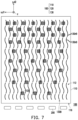
- FIG. 7 is a schematic bottom view of a backlight module according to still another embodiment of the invention.
- FIG. 8 is a schematic bottom view of a backlight module according to yet another embodiment of the invention.
- FIG. 9 is a schematic bottom view of a backlight module according to an embodiment of the invention.
- FIG. 10 A is a schematic bottom view of a backlight module according to another embodiment of the invention.
- FIG. 10 B is a schematic cross-sectional view of a backlight module according to another embodiment of the invention.
- FIG. 10 C is a schematic top view of a sub-optical microstructure of a second optical microstructure according to another embodiment of the invention.
- FIG. 10 D is a schematic three-dimensional view of a sub-optical microstructure of the second optical microstructure according to another embodiment of the invention.
- FIG. 10 E illustrates a sub-optical microstructure of a second optical microstructure and a projection thereof on a reference plane according to another embodiment of the invention.
- FIG. 10 F illustrates a projection of the sub-optical microstructure of the second optical microstructure on the reference plane according to another embodiment of the invention.
- FIG. 10 G illustrates a projection of a sub-optical microstructure of a second optical microstructure on the reference plane according to still another embodiment of the invention.
- FIG. 11 A is a schematic bottom view of a backlight module according to yet another embodiment of the invention.
- FIG. 11 B is a schematic cross-sectional view of the backlight module according to yet another embodiment of the invention.
- FIG. 11 C is a schematic three-dimensional view of a second optical microstructure according to yet another embodiment of the invention.
- FIG. 12 A is a schematic top view of a sub-optical microstructure of a second optical microstructure according to an embodiment of the invention.
- FIG. 12 B is a schematic cross-sectional view of the sub-optical microstructure of the second optical microstructure according to an embodiment of the invention.
- FIG. 13 A is a schematic top view of a sub-optical microstructure of a second optical microstructure according to another embodiment of the invention.
- FIG. 13 B is a schematic cross-sectional view of the sub-optical microstructure of the second optical microstructure according to another embodiment of the invention.
- FIG. 14 A is a schematic top view of a sub-optical microstructure of a second optical microstructure according to still another embodiment of the invention.
- FIG. 14 B is a schematic cross-sectional view of the sub-optical microstructure of the second optical microstructure according to still another embodiment of the invention.
- FIG. 15 A is a schematic top view of a sub-optical microstructure of a second optical microstructure according to yet another embodiment of the invention.
- FIG. 15 B is a schematic cross-sectional view of the sub-optical microstructure of the second optical microstructure according to yet another embodiment of the invention.
- FIG. 16 A is a schematic top view of a sub-optical microstructure of a second optical microstructure according to an embodiment of the invention.
- FIG. 16 B is a schematic three-dimensional view of the sub-optical microstructure of the second optical microstructure according to an embodiment of the invention.
- FIG. 16 C is a schematic side view of the sub-optical microstructure of the second optical microstructure according to an embodiment of the invention.
- FIG. 17 A is a schematic top view of a sub-optical microstructure of a second optical microstructure according to another embodiment of the invention.
- FIG. 17 B is a schematic three-dimensional view of the sub-optical microstructure of the second optical microstructure according to another embodiment of the invention.
- FIG. 17 C is a schematic side view of the sub-optical microstructure of the second optical microstructure according to another embodiment of the invention.
- FIG. 18 A is a schematic top view of a sub-optical microstructure of a second optical microstructure according to still another embodiment of the invention.
- FIG. 18 B is a schematic three-dimensional view of the sub-optical microstructure of the second optical microstructure according to still another embodiment of the invention.
- FIG. 19 A is a schematic top view of a sub-optical microstructure of a second optical microstructure according to yet another embodiment of the invention.
- FIG. 19 B is a schematic three-dimensional view of the sub-optical microstructure of the second optical microstructure according to yet another embodiment of the invention.
- FIG. 20 A is a schematic top view of a second optical microstructure according to an embodiment of the invention.
- FIG. 20 B is a schematic cross-sectional view of the second optical microstructure according to an embodiment of the invention.
- FIG. 20 C is a schematic three-dimensional view of the second optical microstructure according to an embodiment of the invention.
- FIG. 21 A is a schematic top view of a first optical microstructure according to another embodiment of the invention.
- FIG. 21 B is a schematic cross-sectional view of the first optical microstructure according to another embodiment of the invention.
- FIG. 21 C is a schematic three-dimensional view of the first optical microstructure according to another embodiment of the invention.
- FIG. 22 A is a schematic top view of a first optical microstructure according to still another embodiment of the invention.
- FIG. 22 B is a schematic cross-sectional view of the first optical microstructure according to still another embodiment of the invention.
- FIG. 22 C is a schematic three-dimensional view of the first optical microstructure according to still another embodiment of the invention.
- FIG. 23 A is a schematic top view of a first optical microstructure according to yet another embodiment of the invention.
- FIG. 23 B is a schematic cross-sectional view of the first optical microstructure according to yet another embodiment of the invention.
- FIG. 23 C is a schematic three-dimensional view of the first optical microstructure according to yet another embodiment of the invention.
- FIG. 24 A is a schematic three-dimensional view of a first optical microstructure according to an embodiment of the invention.
- FIG. 24 B is a cross section of the first optical microstructure according to an embodiment of the invention.
- FIG. 24 C is a schematic cross-sectional view of the first optical microstructure according to an embodiment of the invention.
- FIG. 25 is a schematic bottom view of a part of a backlight module according to yet another embodiment of the invention.
- FIG. 26 is a schematic bottom view of a part of a backlight module according to an embodiment of the invention.
- FIG. 27 is a schematic bottom view of a part of a backlight module according to another embodiment of the invention.
- FIG. 28 A is a schematic top view of a sub-optical microstructure of a second optical microstructure according to an embodiment of the invention.
- FIG. 28 B is a schematic three-dimensional view of the sub-optical microstructure of the second optical microstructure according to an embodiment of the invention.
- FIG. 28 C is a schematic side view of the sub-optical microstructure of the second optical microstructure according to an embodiment of the invention.
- FIG. 28 D is a schematic cross-sectional view of the sub-optical microstructure of the second optical microstructure according to an embodiment of the present invention.
- the description of “A” component facing “B” component herein may contain the situations that “A” component directly faces “B” component or one or more additional components are between “A” component and “B” component.
- the description of “A” component “adjacent to” “B” component herein may contain the situations that “A” component is directly “adjacent to” “B” component or one or more additional components are between “A” component and “B” component. Accordingly, the drawings and descriptions will be regarded as illustrative in nature and not as restrictive.
- FIG. 1 A is a schematic bottom view of a backlight module according to an embodiment of the invention.
- FIG. 1 B is a schematic cross-sectional view of the backlight module according to an embodiment of the invention.
- FIG. 1 B corresponds to a section line I-I′ of FIG. 1 A .
- a backlight module 10 includes a light guide element 100 .
- the light guide element 100 includes a main body 110 .
- the main body 110 has a bottom surface 112 , a light emitting surface 114 and a light incident surface 116 .
- the light emitting surface 114 is opposite to the bottom surface 112 .
- the light incident surface 116 is connected between the light emitting surface 114 and the bottom surface 112 .
- the backlight module 10 further includes a light source 200 , which is disposed beside the light incident surface 116 and configured to emit a light beam 1 .
- the light source 200 may include light-emitting diode elements.
- the invention is not limited thereto, and in other embodiments, the light source 200 may also include other types of light-emitting elements.
- an x-axis direction x, the y-axis direction y and the z-axis direction z that are perpendicular to each other are drawn, where the x-axis direction x is parallel to the light incident surface 116 of the main body 110 of the light guide element 100 , the y-axis direction y is perpendicular to the light incident surface 116 of the main body 110 of the light guide element 100 , and the z-axis direction z is perpendicular to the bottom surface 112 of the main body 110 of the light guide element 100 .
- FIG. 2 A is a schematic top view of a first optical microstructure according to an embodiment of the invention.
- FIG. 2 B is a schematic cross-sectional view of the first optical microstructure according to an embodiment of the invention.
- FIG. 2 C is a schematic three-dimensional view of the first optical microstructure according to an embodiment of the invention. It should be noted that, for the convenience of illustration and description, the first optical microstructures 120 shown in FIG. 2 A to FIG. 2 C are shown as complementary to the first optical microstructure 120 shown in FIG. 1 B .
- the light guide element 100 further includes a plurality of first optical microstructures 120 , which are recessed into or protrude from the bottom surface 112 , where each first optical microstructure 120 has a first surface 122 and a second surface 124 .
- the first surface 122 and the second surface 124 may selectively form the first optical microstructures 120 recessed in the bottom surface 112 , and the first surface 122 may be located between the light incident surface 116 and the second surface 124 .
- the invention is not limited thereto.
- the first surface 122 and the second surface 124 may also form a first optical microstructure protruding from the bottom surface 112 , which will be described in the following paragraphs with reference of other drawings.
- a function of the first optical microstructures 120 is to deflect the light beam 1 out of the light guide element 100 .
- the light beam 1 is reflected at an interface between the first surface 122 and an environmental medium (for example, air), thus destroying the total internal reflection of the light beam 1 in the light guide element 100 , so that the light beam 1 emits from the light emitting surface 114 .
- an environmental medium for example, air
- an orthogonal projection of the first optical microstructure 120 on the bottom surface 112 may roughly present a barrel shape encircled by two arcs and two straight lines.
- the invention does not limit the shape of the first optical microstructure 120 as long as the first optical microstructure 120 may destroy the total internal reflection to make the light beam 1 to emit from the light emitting surface 114 .
- the first optical microstructure 120 may also have other shapes, which will be exemplified in the following paragraphs with reference of other drawings.
- FIG. 3 A is a schematic top view of a sub-optical microstructure of a second optical microstructure according to an embodiment of the invention.
- FIG. 3 B is a schematic three-dimensional view of the sub-optical microstructure of the second optical microstructure according to an embodiment of the invention.
- FIG. 3 C is a schematic three-dimensional view of a part of the light guide element and a part of the second optical microstructure according to an embodiment of the invention.
- FIG. 3 D illustrates the sub-optical microstructure of the second optical microstructure and a projection thereof on a reference plane according to an embodiment of the invention.
- FIG. 3 E illustrates the sub-optical microstructure of the second optical microstructure and a projection thereof on the reference plane according to an embodiment of the invention.
- FIG. 3 A is a schematic top view of a sub-optical microstructure of a second optical microstructure according to an embodiment of the invention.
- FIG. 3 B is a schematic three-dimensional view of the sub-optical microstructure of the second optical microstructure according to
- FIG. 3 F illustrates a main body of the light guide element and a projection of the sub-optical microstructure of the second optical microstructure on the reference plane according to an embodiment of the invention. It should be noted that, for the convenience of illustration and description, the second optical microstructure 130 shown in FIG. 3 A , FIG. 3 B , FIG. 3 D and FIG. 3 E are shown as complementary to the second optical microstructure 130 shown in FIG. 1 B .
- the light guide element 100 further includes a plurality of second optical microstructures 130 , which are recessed into or protrude from the bottom surface 112 .
- the plurality of second optical microstructures 130 include a plurality of sub-optical microstructures 130 r .
- at least one second optical microstructure 130 is disposed between two adjacent first optical microstructures 120 .
- the bottom surface 112 has a square partition region R 1 , and a side length L R1 of the partition region R 1 is 20 mm.
- adjacent two of the plurality of first optical microstructures 120 have a first pitch P 1 , if the first pitch P 1 is greater than 60 ⁇ m, at least one of the plurality of second optical microstructures 130 is disposed between the adjacent two of the plurality of first optical microstructures 120 .
- the plurality of second optical microstructures 130 are arranged in an arrangement direction d 1
- the plurality of sub-optical microstructures 130 r of each second optical microstructure 130 are connected to each other in an extending direction d 2
- each of the sub-optical microstructures 130 r extends in the extending direction d 2
- the arrangement direction d 1 and the extending direction d 2 are intersected.
- the second optical microstructure 130 may be selectively recessed into the bottom surface 112 of the main body 110 of the light guide element 100 .
- the invention is not limited thereto.
- the second optical microstructure 130 may protrude from the bottom surface 112 , which will be exemplified in the following paragraphs with reference of other drawings.
- a first acute angle ⁇ 1 is included with the first surface 122 of the first optical microstructure 120 and the bottom surface 112 of the main body 110 of the light guide element 100 , and the first acute angle ⁇ 1 is a first angle of the first optical microstructure 120 , and an angle value of the first angle is V1, where V1>0.
- V1 0.5° ⁇ 1 ⁇ 30°, i.e., 0.5 ⁇ V1 ⁇ 30, but the invention is not limited thereto.
- a projection 130 rs (indicated in FIG. 3 D , FIG. 3 E and FIG. 3 F ) of each sub-optical microstructure 130 r of the second optical microstructure 130 on a reference plane P yz perpendicular to the light incident surface 116 has a peak point m closest to the light emitting surface 114 and a first valley point a and a second valley point b farthest from the light emitting surface 114 , the peak point m is located between the first valley point a and the second valley point b, and the first valley point a is located between the light incident surface 116 and the second valley point b.
- the reference plane P yz is, for example, a plane formed by the y-axis direction y and the z-axis direction z.
- the first valley point a, the peak point m, and the second valley point b shown in FIG. 3 D and FIG. 3 E respectively correspond to a point A, a point M, and a point B on a ridgeline 138 shown in FIGS. 3 A and 3 B .
- a height difference between the peak point m and the first valley point a in the z-axis direction z perpendicular to the bottom surface 112 is ⁇ H
- a length difference between the peak point m and the first valley point a in the y-axis direction y perpendicular to the light incident surface 116 is ⁇ L
- a value obtained by tan ⁇ 1 ( ⁇ H/ ⁇ L) is V2, where V2>0 and V2 ⁇ 0.5 ⁇ V1.
- the backlight module 10 further includes a reflective sheet 300 disposed under the bottom surface 112 of the main body 110 of the light guide element 100 .
- a function of the second optical microstructures 130 is to make the light guide element 100 to still have sufficient air gaps g between a low-density area of the first optical microstructures 120 and the reflective sheet 300 , so as to prevent adsorption of the reflective sheet 300 to the light guide element 100 .
- V2 ⁇ 0.5 ⁇ V1 the arrangement of the second optical microstructures 130 will not excessively affect a light output distribution of the backlight module 10 .
- the arrangement of the second optical microstructure 130 may mitigate an adverse phenomenon (for example, slight whitening at a position where the reflective sheet 300 leans against the light guide element 100 ) caused by adsorption between the reflective sheet 300 and the light guide element 100 without excessively affecting the light output distribution of the backlight module 10 .
- an arrangement density of the first optical microstructures 120 increases as a distance from the first optical microstructures 120 to the light incident surface 116 increases, and an arrangement density of the second optical microstructures 130 decreases as a distance from the second optical microstructures 130 to the light incident surface 116 increases.
- the arrangement density of the first optical microstructures 120 is low, and the second optical microstructures 130 located outside the first optical microstructures 120 occupy a large area, so that the second optical microstructures 130 located outside the first optical microstructures 120 show a high arrangement density.
- the arrangement density of the first optical microstructures 120 is high, and the second optical microstructures 130 located outside the first optical microstructures 120 occupy a small area, so that the second optical microstructures 130 located outside the first optical microstructures 120 show a low arrangement density.
- tendency of the arrangement densities of the first optical microstructures 120 and the second optical microstructures 130 are opposite.
- the arrangement density of the first optical microstructures 120 becomes lower, the arrangement density of the second optical microstructures 130 becomes higher, so that the second optical microstructures 130 may fill vacancies between the plurality of first optical microstructures 120 , thereby reducing the probability of the reflective sheet 300 adsorbing the main body 110 of the light guide element 100 at a place where the arrangement density of the first optical microstructures 120 is low.
- the plurality of second optical microstructures 130 are arranged in the arrangement direction d 1 , and in a region of the bottom surface 112 close to the light incident surface 116 (for example, the partition region R 1 ), two adjacent first optical microstructures 120 have a first pitch P 1 in the arrangement direction d 1 , two adjacent second optical microstructures 130 have a second pitch P 2 in the arrangement direction d 1 , and the second pitch P 2 is smaller than the first pitch P 1 .
- the second optical microstructures 130 are not only interspersed between the first optical microstructures 120 , but also arranged more closely compared to the first optical microstructures 120 .
- the plurality of second optical microstructures 130 are arranged in the arrangement direction d 1 , and each of the second optical microstructures 130 includes the plurality of sub-optical microstructures 130 r , where the plurality of sub-optical microstructures 130 r included in each second optical microstructure 130 are connected to each other in the extending direction d 2 , each sub-optical microstructure 130 r extends in the extending direction d 2 , and the arrangement direction d 1 and the extending direction d 2 are intersected.
- the arrangement direction d 1 may be selectively consistent with the x-axis direction x (i.e., the arrangement direction d 1 may be selectively parallel to the light incident surface 116 ), and the extending direction d 2 may be selectively consistent with the y-axis direction y (i.e., the extending direction d 2 may be selectively perpendicular to the light incident surface 116 ), but the invention is not limited thereto.
- an orthogonal projection of each sub-optical microstructure 130 r of each second optical microstructure 130 on the bottom surface 112 includes a curved pattern 136
- the curved pattern 136 includes a first sub-curved pattern 136 a and a second sub-curved pattern 136 b respectively protruding toward opposite directions A 1 and A 2
- the plurality of first sub-curved patterns 136 a and the plurality of second sub-curved patterns 136 b of the plurality of sub-optical microstructures 130 r included in each second optical microstructure 130 are alternately arranged and are connected to each other.
- the plurality of first sub-curved patterns 136 a and the plurality of second sub-curved patterns 136 b of the plurality of sub-optical microstructures 130 r included in each second optical microstructure 130 may be substantially connected to form a wavy strip pattern.
- the invention does not limit the shape of the second optical microstructures 130 , as long as the arrangement of the second optical microstructures 130 makes the reflective sheet 300 and the light guide element 100 to have the air gaps g at the low-density arrangement region (for example, the partition region R 1 ) of the first optical microstructures 120 to result in uneasy adsorption between the reflective sheet 300 and the light guide element 100 .
- the second optical microstructure 130 may have any other shape, which will be exemplified in the following paragraphs with reference of other drawings.
- each sub-optical microstructure 130 r has a ridgeline 138 , and an orthogonal projection of the ridgeline 138 on the bottom surface 112 includes a repeating line segment 138 s , and the repeating line segment 138 s includes a first sub-line segment 138 s 1 and a second sub-line segment 138 s 2 respectively protruding in the opposite directions A 1 and A 2 , where the first sub-line segment 138 s 1 and the second sub-line segment 138 s 2 are connected at an inflection point 138 si of the repeating line segment 138 s , and a first reference line K 1 is tangent to a vertex 138 s 1 v of the first sub-line segment 138 s 1 , a second reference line K 2 is tangent to a vertex 138 s 2 v of the second sub-line segment 138 s 2 , a third reference line K 3 passes through the in
- the repeating line segment 138 s has a length L, the first reference line K 1 and the third reference line K 3 have a first distance D1, and the second reference line K 2 and the third reference line K 3 have a second distance D2, where (D 1 +D 2 ) ⁇ L/10.
- the length L of the repeating line segment 138 s refers to a length of the repeating line segment 138 s in the extending direction d 2 (referring to FIG. 1 A ) of each sub-optical microstructure 130 r
- the length L refers to the length of the repeating line segment 138 s in the y-axis direction y.
- the expression “(D 1 +D 2 ) ⁇ L/10” means that a degree of curvature of the second optical microstructure 130 toward opposite sides is within a certain range. Therefore, even if the second optical microstructure 130 is curved left and right in the x-axis direction x and undulated up and down in the z-axis direction z, the influence of the second optical microstructures 130 on the light output distribution of the backlight module 10 is still within a controllable range. Namely, in the case of configuring the second optical microstructures 130 , the backlight module 10 may still have a uniform light output distribution.
- FIG. 4 A is a schematic three-dimensional view of a sub-optical microstructure of a second optical microstructure of a first comparative example.
- FIG. 4 B illustrates a projection of the sub-optical microstructure of the second optical microstructure of the first comparative example on a reference plane.
- a projection 130 rs ′ of a sub-optical microstructure 130 r ′ of a second optical microstructure 130 ′ of the first comparative example on the reference plane P yz has a first valley point a, a peak point m and a second valley point b, a height difference between the peak point m and the first valley point a in the z-axis direction z is ⁇ H, a length difference between the peak point m and the first valley point a in the y-axis direction y is ⁇ L, and a value obtained by tan ⁇ 1 ( ⁇ H/ ⁇ L) is V2.
- the sub-optical microstructure of the second optical microstructure of the first comparative example have a steeper structural surface between the corresponding peak point m and the first valley point a, and the steeper structural surface is likely to cause destroying of the total internal reflection of the light beam in the light guide element to result in a fact that the light emits from the light-emitting surface, which will increase the influence on the light output distribution of the backlight module.
- FIG. 5 A is a schematic three-dimensional view of a sub-optical microstructure of a second optical microstructure of a second comparative example.
- FIG. 5 B illustrates a projection of the sub-optical microstructure of the second optical microstructure of the second comparative example on a reference plane.
- a projection 130 rs ′′ of a sub-optical microstructure 130 r ′′ of a second optical microstructure 130 ′′ of the second comparative example on the reference plane P yz has a first valley point a, a peak point m and a second valley point b, a height difference between the peak point m and the first valley point a in the z-axis direction z is ⁇ H, a length difference between the peak point m and the first valley point a in the y-axis direction y is ⁇ L, and a value obtained by tan ⁇ 1 ( ⁇ H/ ⁇ L) is V2.
- the sub-optical microstructure of the second optical microstructure of the second comparative example have a steeper structural surface between the corresponding peak point m and the first valley point a, and the steeper structural surface is likely to cause destroying of the total internal reflection of the light beam in the light guide element to result in a fact that the light emits from the light-emitting surface, which will increase the influence on the light output distribution of the backlight module.
- FIG. 6 A is a schematic cross-sectional view of a backlight module according to another embodiment of the invention.
- FIG. 6 B is a schematic three-dimensional view of a part of a light guide element and a part of a second optical microstructure according to another embodiment of the invention.
- FIG. 6 C illustrates a sub-optical microstructure of a second optical microstructure and a projection thereof on a reference plane according to another embodiment of the invention.
- FIG. 6 D illustrates a sub-optical microstructure of a second optical microstructure and a projection thereof on a reference plane according to another embodiment of the invention.
- FIG. 6 E illustrates a projection of a main body of a light guide element and a projection of a sub-optical microstructure of a second optical microstructure on a reference plane according to another embodiment of the invention.
- a backlight module 10 A of the embodiment is similar to the aforementioned backlight module 10 , a difference there between is that in the embodiment of FIG. 6 A to FIG. 6 E , a first optical microstructure 120 A and a second optical microstructure 130 A protrude from the bottom surface 112 of the main body 110 of the light guide element 100 .
- a projection 130 rs A of each sub-optical microstructure 130 r A of the second optical microstructure 130 A on the reference plane P yz perpendicular to the light incident surface 116 has a peak point m farthest from the light emitting surface 114 and a first valley point a and a second valley point b closest to the light emitting surface 114 , the peak point m is located between the first valley point a and the second valley point b, the first valley point a is located between the light incident surface 116 and the second valley point b, a height difference between the peak point m and the second valley point b in the z-axis direction z perpendicular to the bottom surface 112 is ⁇ H, and a length difference between the peak point m and the second valley point b in the y-axis direction y perpendicular to the light incident surface 116 is ⁇ L
- FIG. 7 is a schematic bottom view of a backlight module according to still another embodiment of the invention.
- a backlight module 10 B of FIG. 7 is similar to the backlight module 10 of FIG. 1 A , and a difference there between is that a second optical microstructure 130 B of the backlight module 10 B of FIG. 7 is different from the second optical microstructure 130 of the backlight module 10 A of FIG. 4 A .
- a plurality of second optical microstructures 130 B are arranged in the arrangement direction d 1 , and a plurality of sub-optical microstructures 130 r B of each second optical microstructure 130 B are spaced apart from each other in the extending direction d 2 , each of the sub-optical microstructures 130 r B extends in the extending direction d 2 , and the arrangement direction d 1 is intersected with the extending direction d 2 .
- each of the second optical microstructures 130 B may include the plurality of sub-optical microstructures 130 r B disconnected from each other.
- the plurality of sub-optical microstructures 130 r B of each second optical microstructure 130 B may be arranged on a same wavy line, but the invention is not limited thereto. In other non-illustrated embodiments, the plurality of sub-optical microstructures 130 r B may also be arranged in random distribution.
- FIG. 8 is a schematic bottom view of a backlight module according to yet another embodiment of the invention.
- a backlight module 10 C of FIG. 8 is similar to the backlight module 10 of FIG. 1 A , and a difference there between is that a second optical microstructure 130 C of the backlight module 10 C of FIG. 8 is different from the second optical microstructure 130 of the backlight module 10 of FIG. 1 A .
- an orthogonal projection of the second optical microstructure 130 C on the bottom surface 112 may be a linear stripe pattern.
- FIG. 9 is a schematic bottom view of a backlight module according to an embodiment of the invention.
- a backlight module 10 D of FIG. 9 is similar to the backlight module 10 C of FIG. 8 , and a difference there between is that a second optical microstructure 130 D of the backlight module 10 D of FIG. 9 is different from the second optical microstructure 130 C of the backlight module 10 C of FIG. 8 .
- a plurality of sub-optical microstructures 130 r D of each second optical microstructure 130 D are spaced apart from each other in the extending direction d 2 .
- FIG. 10 A is a schematic bottom view of a backlight module according to another embodiment of the invention.
- FIG. 10 B is a schematic cross-sectional view of a backlight module according to another embodiment of the invention.
- FIG. 10 B corresponds to a section line II-II′ of FIG. 10 A .
- FIG. 10 C is a schematic top view of a sub-optical microstructure of a second optical microstructure according to another embodiment of the invention.
- FIG. 10 D is a schematic three-dimensional view of a sub-optical microstructure of the second optical microstructure according to another embodiment of the invention.
- FIG. 10 E illustrates a sub-optical microstructure of a second optical microstructure and a projection thereof on a reference plane according to another embodiment of the invention.
- FIG. 10 E illustrates a sub-optical microstructure of a second optical microstructure and a projection thereof on a reference plane according to another embodiment of the invention.
- 10 F illustrates a projection of the sub-optical microstructure of the second optical microstructure on the reference plane according to another embodiment of the invention. It should be noted that for the convenience of illustration and description, the second optical microstructure 130 E presented in FIG. 10 C to 10 F are illustrated as being complementary to the second optical microstructure 130 E presented in FIG. 10 B .
- a backlight module 10 E of the embodiment is similar to the aforementioned backlight module 10 , and a difference there between is that an arrangement of the second optical microstructures 130 E of the backlight module 10 E of the embodiment is different from the arrangement of the second optical microstructures 130 of the aforementioned backlight module 10 .
- the first surface 122 of the first optical microstructure 120 and the bottom surface 112 of the main body 110 of the light guide element 100 include a first acute angle ⁇ 1 , the first acute angle ⁇ 1 is a first angle of the first optical microstructure 120 , and an angle value of the first angle is V1, where V1>0.
- a projection 130 rs E of each sub-optical microstructure 130 r E of the second optical microstructure 130 E on the reference plane P yz perpendicular to the light incident surface 116 has a peak point m closest to the light emitting surface 114 and a first valley point a and a second valley point b farthest from the light emitting surface 114 , where the peak point m is located between the first valley point a and the second valley point b, and the first valley point a is located between the light incident surface 116 and the second valley point b.
- the reference plane P yz is, for example, a plane in which the y-axis direction y and the z-axis direction z are located.
- the first valley point a, the peak point m, and the second valley point b shown in FIG. 10 F respectively correspond to points A, M, and B on the ridgeline 138 of the sub-optical microstructure 130 r E shown in FIG. 10 E .
- a height difference between the peak point m and the first valley point a in the z-axis direction z perpendicular to the bottom surface 112 is ⁇ H
- a length difference between the peak point m and the first valley point a in the y-axis direction y perpendicular to the light incident surface 116 is ⁇ L
- a value obtained by tan ⁇ 1 ( ⁇ H/ ⁇ L) is V2, where V2>0, and V2 ⁇ 0.5 ⁇ V1.
- a difference from the aforementioned backlight module 10 is that in the embodiment, the plurality of second optical microstructures 130 E are arranged in the arrangement direction d 1 , the plurality of sub-optical microstructures 130 r E included in each second optical microstructure 130 E are arranged in the extending direction d 2 , each sub-optical microstructure 130 r E extends in the extending direction d 2 , the arrangement direction d 1 is intersected with the extending direction d 2 , and the extending direction d 2 is parallel to the light incident surface 116 , namely, in the embodiment, the extending direction d 2 may be selectively consistent with the x-axis direction x.
- FIG. 10 G illustrates a projection of a sub-optical microstructure of a second optical microstructure on the reference plane according to still another embodiment of the invention.
- the second optical microstructure 130 F protrude from the bottom surface 112 of the main body 110 of the light guide element 100 (referring to FIG. 10 B together).
- a projection 130 rs F of each sub-optical microstructure 130 r F of the second optical microstructure 130 F on the reference plane P yz perpendicular to the light incident surface 116 has a peak point m farthest from the light emitting surface 114 and a first valley point a and a second valley point b closest to the light emitting surface 114 .
- the peak point m is located between the first valley point a and the second valley point b
- the first valley point a is located between the light incident surface 116 and the second valley point b
- a height difference between the peak point m and the second valley point b in the z-axis direction z perpendicular to the bottom surface 112 is ⁇ H
- a length difference between the peak point m and the second valley point b in the y-axis direction y perpendicular to the light incident surface 116 is ⁇ L
- a value obtained by tan ⁇ 1 ( ⁇ H/ ⁇ L) is V2, where V2>0, and V2 ⁇ 0.5 ⁇ V1.
- FIG. 11 A is a schematic bottom view of a backlight module according to yet another embodiment of the invention.
- FIG. 11 B is a schematic cross-sectional view of the backlight module according to yet another embodiment of the invention.
- FIG. 11 B corresponds to a section line of FIG. 11 A .
- FIG. 11 C is a schematic three-dimensional view of a second optical microstructure according to yet another embodiment of the invention. It should be noted that, for the convenience of illustration and description, the second optical microstructure 130 G presented in FIG. 7 C is illustrated as a situation complementary to the second optical microstructure 130 G presented in FIG. 7 B .
- a backlight module 10 G of FIG. 11 A is similar to the backlight module 10 of FIG. 1 A , and a difference there between is that a second optical microstructure 130 G of the backlight module 10 G of FIG. 11 A is different from the second optical microstructure 130 of the backlight module 10 of FIG. 1 A .
- each second optical microstructure 130 G includes a side surface 133 and an opposing surface 135 , the opposing surface 135 is disposed opposite to the bottom surface 112 , the side surface 133 is connected between the bottom surface 112 and the opposing surface 135 , and the side surface 133 and the bottom surface 112 have a first boundary B 1 , the side surface 133 and the opposing surface 135 have a second boundary B 2 , an orthogonal projection of the second boundary B 2 on the bottom surface 112 is located within an orthogonal projection of the first boundary B 1 on the bottom surface 112 , and a shape of the orthogonal projection of the first boundary B 1 is different from a shape of the orthogonal projection of the second boundary B 2 .
- the first boundary B 1 may be a circle or an ellipse with a larger area
- the second boundary B 2 may be a circle or an ellipse with a smaller area
- the orthogonal projection of the second boundary B 2 on the bottom surface 112 falls within the orthogonal projection of the first boundary B 1 on the bottom surface 112 , but the invention is not limited thereto.
- one second optical microstructure 130 G may be regarded as a sub-optical microstructure.
- the second optical microstructure 130 G of FIG. 11 A to FIG. 11 C is shown as extending along the x-axis direction x, i.e., a long-axis direction of the ellipse presented by the first boundary B 1 is the x-axis direction x, and a long-axis direction of the ellipse presented by the second boundary B 2 is the x-axis direction x, but in other embodiments, the second optical microstructure 130 G may also be rotated by a certain angle for placement, for example, rotated by 90 degrees, so that the second optical microstructure extends along the y-axis direction y, i.e., the long axis direction of the ellipse presented by the first boundary B 1 may be changed to the y-axis direction y, and the long-axis direction of the ellipse presented by the second boundary B 2 may be changed to the y-axis direction y.
- the second optical microstructures 130 G may be arranged on the bottom surface 112 of the main body 110 of the light guide element 100 in the form of a regular matrix or a random distribution, or the second optical microstructures 130 G extending in different directions may also be adopted.
- FIG. 12 A is a schematic top view of a sub-optical microstructure of a second optical microstructure according to an embodiment of the invention.
- FIG. 12 B is a schematic cross-sectional view of the sub-optical microstructure of the second optical microstructure according to an embodiment of the invention.
- a cross section of a sub-optical microstructure 130 r H of a second optical microstructure 130 H on a plane where the x-axis direction x and the z-axis direction z are located has two concave arc line segments.
- FIG. 13 A is a schematic top view of a sub-optical microstructure of a second optical microstructure according to another embodiment of the invention.
- FIG. 13 B is a schematic cross-sectional view of the sub-optical microstructure of the second optical microstructure according to another embodiment of the invention.
- a cross section of a sub-optical microstructure 130 r I of a second optical microstructure 130 I on the plane where the x-axis direction x and the z-axis direction z are located has a convex arc line segment.
- FIG. 14 A is a schematic top view of a sub-optical microstructure of a second optical microstructure according to still another embodiment of the invention.
- FIG. 14 B is a schematic cross-sectional view of the sub-optical microstructure of the second optical microstructure according to still another embodiment of the invention.
- a cross section of a sub-optical microstructure 130 r J of a second optical microstructure 130 J on the plane where the x-axis direction x and the z-axis direction z are located has two convex arc line segments, and a connection point 138 Jp of the two convex arc line segments is a point on a ridgeline 138 J of the sub-optical microstructure 130 r J of the second optical microstructure 130 J.
- FIG. 15 A is a schematic top view of a sub-optical microstructure of a second optical microstructure according to yet another embodiment of the invention.
- FIG. 15 B is a schematic cross-sectional view of the sub-optical microstructure of the second optical microstructure according to yet another embodiment of the invention.
- a cross section of a sub-optical microstructure 130 r K of a second optical microstructure 130 K on the plane where the x-axis direction x and the z-axis direction z are located is approximately trapezoidal with two rounded corners
- FIG. 16 A is a schematic top view of a sub-optical microstructure of a second optical microstructure according to an embodiment of the invention.
- FIG. 16 B is a schematic three-dimensional view of the sub-optical microstructure of the second optical microstructure according to an embodiment of the invention.
- FIG. 16 C is a schematic side view of the sub-optical microstructure of the second optical microstructure according to an embodiment of the invention.
- a sub-optical microstructure 130 r L of a second optical microstructure 130 L may include a first sub-optical microstructure 130 r L- 1 , a second sub-optical microstructure 130 r L- 2 and a third sub-optical microstructure 130 r L- 3 arranged in the x-axis direction x, where the second sub-optical microstructure 130 r L- 2 and the third sub-optical microstructure 130 r L- 3 are respectively located at two sides of the first sub-optical microstructure 130 r L- 1 .
- a height H 1 of the first sub-optical microstructure 130 r L- 1 in the z-axis direction z is greater than a height H 2 of the second sub-optical microstructure 130 r L- 2 in the z-axis direction z and a height H 3 of the third sub-optical microstructure 130 r L- 3 in the z-axis direction z.
- the height H 1 of the first sub-optical microstructure 130 r L- 1 in the z-axis direction z, the height H 2 of the second sub-optical microstructure 130 r L- 2 in the z-axis direction z, and the height H 3 of the third sub-optical microstructure 130 r L- 3 in the z-axis direction z are fixed.
- FIG. 17 A is a schematic top view of a sub-optical microstructure of a second optical microstructure according to another embodiment of the invention.
- FIG. 17 B is a schematic three-dimensional view of the sub-optical microstructure of the second optical microstructure according to another embodiment of the invention.
- FIG. 17 C is a schematic side view of the sub-optical microstructure of the second optical microstructure according to another embodiment of the invention.
- a sub-optical microstructure 130 r M of a second optical microstructure 130 M of FIG. 17 A to FIG. 17 C is similar to the sub-optical microstructure 130 r L of the second optical microstructure 130 L of FIG. 16 A to FIG. 16 C , and a difference there between is that in the embodiment of FIG. 17 A to FIG. 17 C , the height H 1 of a first sub-optical microstructure 130 r M- 1 in the z-axis direction z, the height H 2 of a second sub-optical microstructure 130 r M- 2 in the z-axis direction z, and the height H 3 of a third sub-optical microstructure 130 r M- 3 in the z-axis direction z fluctuate.
- FIG. 18 A is a schematic top view of a sub-optical microstructure of a second optical microstructure according to still another embodiment of the invention.
- FIG. 18 B is a schematic three-dimensional view of the sub-optical microstructure of the second optical microstructure according to still another embodiment of the invention.
- a sub-optical microstructure 130 rN of a second optical microstructure 130 N of FIG. 18 A to FIG. 18 C is similar to the sub-optical microstructure 130 r of the second optical microstructure 130 of FIG. 3 A to FIG. 3 B , and a difference there between is that in the embodiment of FIG. 18 A to FIG.
- each second optical microstructure 130 N includes the plurality of sub-optical microstructures 130 rN, and the plurality of sub-optical microstructures 130 rN included in each second optical microstructure 130 N are arranged in the extending direction d 2 , and a width W of each sub-optical microstructure 130 rN in the arrangement direction d 1 is gradually changed.
- the width W of the sub-optical microstructure 130 rN gradually decreases from the inflection point 138 si of the ridgeline 138 to the upper and lower sides.
- FIG. 19 A is a schematic top view of a sub-optical microstructure of a second optical microstructure according to yet another embodiment of the invention.
- FIG. 19 B is a schematic three-dimensional view of the sub-optical microstructure of the second optical microstructure according to yet another embodiment of the invention.
- a sub-optical microstructure 130 r O of a second optical microstructure 130 O of FIG. 19 A to FIG. 19 B is similar to the sub-optical microstructure 130 rN of the second optical microstructure 130 N of FIG. 18 A to FIG. 18 B , and a difference there between is that in the embodiment of FIG. 19 A to FIG. 19 C , a width W of the sub-optical microstructure 130 r O in the arrangement direction d 1 gradually increases from the inflection point 138 si of the ridgeline 138 to the upper and lower sides.
- FIG. 20 A is a schematic top view of a second optical microstructure according to an embodiment of the invention.
- FIG. 20 B is a schematic cross-sectional view of the second optical microstructure according to an embodiment of the invention.
- FIG. 20 C is a schematic three-dimensional view of the second optical microstructure according to an embodiment of the invention.
- an orthogonal projection of each second optical microstructure 130 P on the bottom surface 112 has an outer profile 130 Po
- the outer profile 130 Po includes a first curved section 130 Po- 1 and a second curved section 130 Po- 2 disposed opposite to each other.
- the first curved section 130 Po- 1 and the second curved section 130 Po- 2 respectively protrude toward opposite directions.
- the outer profile 130 Po of the second optical microstructure 130 P may be approximately spindle-shaped.
- a radius of curvature of the first curved section 130 Po- 1 is greater than a radius of curvature of the second curved section 130 Po- 2 , a light-facing area of the second optical microstructure 130 P is reduced, thereby reducing the influence on the light output distribution of the backlight module.
- the various second optical microstructures of FIGS. 12 A- 20 C are shown as extending along the y-axis direction y, but in other embodiments, the various second optical microstructures of FIGS. 12 A- 20 C may also be rotated by a certain angle for placement, for example, rotated by 90 degrees, so that the second optical microstructure extends along the x-axis direction x.
- FIG. 21 A is a schematic top view of a first optical microstructure according to another embodiment of the invention.
- FIG. 21 B is a schematic cross-sectional view of the first optical microstructure according to another embodiment of the invention.
- FIG. 21 B corresponds to a section line IV-IV′ of FIG. 21 A .
- FIG. 21 C is a schematic three-dimensional view of the first optical microstructure according to another embodiment of the invention.
- a difference between a first optical microstructure 120 Q of the embodiment and the aforementioned first optical microstructure 120 is that in the embodiment, an orthogonal projection of the first optical microstructure 120 Q on the bottom surface 112 (referring to FIG. 1 A and FIG. 1 B ) may be rectangular.
- FIG. 22 A is a schematic top view of a first optical microstructure according to still another embodiment of the invention.
- FIG. 22 B is a schematic cross-sectional view of the first optical microstructure according to still another embodiment of the invention.
- FIG. 22 B corresponds to a section line V-V′ of FIG. 22 A .
- FIG. 22 C is a schematic three-dimensional view of the first optical microstructure according to still another embodiment of the invention.
- a difference between a first optical microstructure 120 R of the embodiment and the aforementioned first optical microstructure 120 is that in the embodiment, an orthogonal projection of the first optical microstructure 120 R on the bottom surface 112 (referring to FIG. 1 A and FIG. 1 B ) is similar to a shape of a floating plate.
- FIG. 23 A is a schematic top view of a first optical microstructure according to yet another embodiment of the invention.
- FIG. 23 B is a schematic cross-sectional view of the first optical microstructure according to yet another embodiment of the invention.
- FIG. 23 B corresponds to a section line VI-VI′ of FIG. 23 A .
- FIG. 23 C is a schematic three-dimensional view of the first optical microstructure according to yet another embodiment of the invention.
- a difference between a first optical microstructure 120 S of the embodiment and the aforementioned first optical microstructure 120 is that in the embodiment, an orthogonal projection of the first optical microstructure 120 S on the bottom surface 112 (referring to FIG. 1 A and FIG. 1 B ) is similar to a fan shape.
- FIG. 24 A is a schematic three-dimensional view of a first optical microstructure according to an embodiment of the invention.
- FIG. 24 B is a cross section of the first optical microstructure according to an embodiment of the invention.
- FIG. 24 C is a schematic cross-sectional view of the first optical microstructure according to an embodiment of the invention.
- a difference between a first optical microstructure 120 T of the embodiment and the aforementioned first optical microstructure 120 is that in the embodiment, an orthogonal projection of the first optical microstructure 120 T on the bottom surface 112 (referring to FIG. 1 A and FIG. 1 B ) is an irregular shape.
- FIG. 25 is a schematic bottom view of a part of a backlight module according to yet another embodiment of the invention.
- a backlight module 10 U of FIG. 25 is similar to the backlight module 10 of FIG. 1 A , and differences there between are as follows.
- the plurality of second optical microstructures 130 are continuous structures and extend across at least one of the plurality of first optical microstructures 120 .
- both of the first optical microstructures 120 and the second optical microstructures 130 may be structures recessed into the bottom surface 112 , where the first optical microstructure 120 is recessed inward from the bottom surface 112 , a part of the second optical microstructure 130 that is not overlapped with the first optical microstructure 120 is recessed inward from the bottom surface 112 , and another part of the second optical microstructure 130 that is overlapped with the first optical microstructure 120 is further recessed inward from the first optical microstructure 120 .
- first optical microstructures 120 and the second optical microstructures 130 may also be structures protruding from the bottom surface 112 , where the first optical microstructures 120 protrude outward from the bottom surface 112 , and a part of the second optical microstructure 130 that is not overlapped with the first optical microstructure 120 protrudes outward from the bottom surface 112 , and another part of the second optical microstructure 130 that is overlapped with the first optical microstructure 120 further protrudes outward from the first optical microstructure 120 .
- the plurality of second optical microstructures 130 are located outside one first optical microstructure 120 , and the plurality of second optical microstructures 130 are connected to an edge 120 e of the first optical microstructure 120 .
- FIG. 26 is a schematic bottom view of a part of a backlight module according to an embodiment of the invention.
- a backlight module 10 V of FIG. 26 is similar to the backlight module 10 of FIG. 1 A , and differences there between are as follows.
- one of the plurality of first optical microstructures 120 has a central area 120 C and a peripheral area 120 P surrounding the central area 120 C
- the plurality of second optical microstructures 130 are overlapped with the peripheral area 120 P of the first optical microstructure 120
- the plurality of second optical microstructures 130 have a plurality of breaks 130 br overlapped with the central area 120 C of the first optical microstructure 120 .
- FIG. 27 is a schematic bottom view of a part of a backlight module according to another embodiment of the invention.
- a backlight module 10 W of FIG. 27 is similar to the backlight module 10 of FIG. 1 A , and differences there between are as follows.
- a part 112 p of the bottom surface 112 surrounds one of the plurality of first optical microstructures 120
- the part 112 p of the bottom surface 112 spaces apart the first optical microstructure 120 and the plurality of second optical microstructures 130 .
- FIG. 28 A is a schematic top view of a sub-optical microstructure of a second optical microstructure according to an embodiment of the invention.
- FIG. 28 B is a schematic three-dimensional view of the sub-optical microstructure of the second optical microstructure according to an embodiment of the invention.
- FIG. 28 C is a schematic side view of the sub-optical microstructure of the second optical microstructure according to an embodiment of the invention.
- FIG. 28 D is a schematic cross-sectional view of the sub-optical microstructure of the second optical microstructure according to an embodiment of the present invention.
- FIG. 28 D corresponds to a section line VII-VII′ of FIG. 28 A .
- a sub-optical microstructure 130 r Q of a second optical microstructure 130 Q may be curved in the z-axis direction z, i.e., a height of the sub-optical microstructure 130 r Q in the z-axis direction z fluctuates.
- the second optical microstructure 130 Q may be used in the backlight module 10 C of FIG. 8 to serve as the second optical microstructure 130 C in FIG. 8 , or may be used in the backlight module 10 D in FIG. 9 to serve as the second optical microstructure 130 D in FIG. 9 , specifically, an orthogonal projection of the sub-optical microstructure 130 r Q of the second optical microstructure 130 Q on the bottom surface 112 of FIG. 8 or FIG. 9 is a linear stripe pattern.
- the backlight module of an embodiment of the invention includes the light guide element and the light-emitting element disposed beside the light incident surface of the light guide element.
- the light guide element includes a plurality of first optical microstructures and a plurality of second optical microstructures that are recessed into or protrude from the bottom surface of the main body, where at least one of the plurality of second optical microstructures is disposed between two adjacent first optical microstructures.
- the value of tan ⁇ 1 ( ⁇ H/ ⁇ L) calculated according to the height difference and the length difference between the peak point and the valley points of the projection of the second optical microstructure on the reference plane perpendicular to the light incident surface is less than or equal to a half of the first angle of the first optical microstructure.
- the first optical microstructures are used for deflecting the light beam emitted by the light-emitting element out of the light guide element.
- the second optical microstructures are used to make enough air gaps existing between the light guide element and the reflective sheet, so as to avoid the adsorption between the reflective sheet and the light guide element, thereby mitigating the adverse caused by the adsorption between the reflective sheet and the light guide element.
- tan ⁇ 1 ( ⁇ H/ ⁇ L) calculated according to the height difference and length difference between the peak point and the valley points of the projection of the second optical microstructure on the reference plane perpendicular to the light incident surface is less than or equal to a half of the first angle of the first optical microstructure, while the second optical microstructures are used to avoid the adsorption between the reflective sheet and the light guide element, the arrangement of the second optical microstructures will not excessively affect the light output distribution of the backlight module.
- the term “the invention”, “the present invention” or the like does not necessarily limit the claim scope to a specific embodiment, and the reference to particularly preferred exemplary embodiments of the invention does not imply a limitation on the invention, and no such limitation is to be inferred.
- the invention is limited only by the spirit and scope of the appended claims. Moreover, these claims may refer to use “first”, “second”, etc. following with noun or element. Such terms should be understood as a nomenclature and should not be construed as giving the limitation on the number of the elements modified by such nomenclature unless specific number has been given.
- the abstract of the disclosure is provided to comply with the rules requiring an abstract, which will allow a searcher to quickly ascertain the subject matter of the technical disclosure of any patent issued from this disclosure.
Landscapes
- Physics & Mathematics (AREA)
- General Physics & Mathematics (AREA)
- Optics & Photonics (AREA)
- Planar Illumination Modules (AREA)
Abstract
Description
Claims (23)
Applications Claiming Priority (2)
| Application Number | Priority Date | Filing Date | Title |
|---|---|---|---|
| CN202210305170.5A CN116840961A (en) | 2022-03-25 | 2022-03-25 | Light guide components and backlight modules |
| CN202210305170.5 | 2022-03-25 |
Publications (2)
| Publication Number | Publication Date |
|---|---|
| US20230305215A1 US20230305215A1 (en) | 2023-09-28 |
| US12253707B2 true US12253707B2 (en) | 2025-03-18 |
Family
ID=88095560
Family Applications (1)
| Application Number | Title | Priority Date | Filing Date |
|---|---|---|---|
| US18/183,118 Active 2043-05-27 US12253707B2 (en) | 2022-03-25 | 2023-03-13 | Light guide element and backlight module |
Country Status (2)
| Country | Link |
|---|---|
| US (1) | US12253707B2 (en) |
| CN (1) | CN116840961A (en) |
Families Citing this family (2)
| Publication number | Priority date | Publication date | Assignee | Title |
|---|---|---|---|---|
| TWI902339B (en) * | 2024-07-08 | 2025-10-21 | 瀚宇彩晶股份有限公司 | Light guide plate and display apparatus |
| CN119001938A (en) * | 2024-10-23 | 2024-11-22 | 苏州弘德光电材料科技有限公司 | Prism structure, viewing angle enlarging film, backlight module and display device |
Citations (8)
| Publication number | Priority date | Publication date | Assignee | Title |
|---|---|---|---|---|
| TWI286225B (en) | 2005-06-08 | 2007-09-01 | Au Optronics Corp | A light guide plate having curved grooves |
| CN200976055Y (en) | 2006-10-18 | 2007-11-14 | 台湾奈普光电科技股份有限公司 | Light guide plate and backlight module |
| US7330315B2 (en) * | 2003-05-02 | 2008-02-12 | Reflexite Corporation | Light-redirecting optical structures |
| TWM331675U (en) | 2007-11-30 | 2008-05-01 | Taiwan Nano Electro Opt Tech | Improved structure for light guide plate |
| US20100085771A1 (en) * | 2008-10-03 | 2010-04-08 | Feng-Li Lin | Light guiding plate |
| US20110267694A1 (en) * | 2010-04-30 | 2011-11-03 | Coretronic Corporation | Optical film |
| US10379268B2 (en) * | 2005-06-09 | 2019-08-13 | Ubright Optronics Corporation | Light directing film |
| TWI707166B (en) | 2018-05-14 | 2020-10-11 | 大陸商瑞儀(廣州)光電子器件有限公司 | Light guide plate, backlight module and display device |
-
2022
- 2022-03-25 CN CN202210305170.5A patent/CN116840961A/en active Pending
-
2023
- 2023-03-13 US US18/183,118 patent/US12253707B2/en active Active
Patent Citations (8)
| Publication number | Priority date | Publication date | Assignee | Title |
|---|---|---|---|---|
| US7330315B2 (en) * | 2003-05-02 | 2008-02-12 | Reflexite Corporation | Light-redirecting optical structures |
| TWI286225B (en) | 2005-06-08 | 2007-09-01 | Au Optronics Corp | A light guide plate having curved grooves |
| US10379268B2 (en) * | 2005-06-09 | 2019-08-13 | Ubright Optronics Corporation | Light directing film |
| CN200976055Y (en) | 2006-10-18 | 2007-11-14 | 台湾奈普光电科技股份有限公司 | Light guide plate and backlight module |
| TWM331675U (en) | 2007-11-30 | 2008-05-01 | Taiwan Nano Electro Opt Tech | Improved structure for light guide plate |
| US20100085771A1 (en) * | 2008-10-03 | 2010-04-08 | Feng-Li Lin | Light guiding plate |
| US20110267694A1 (en) * | 2010-04-30 | 2011-11-03 | Coretronic Corporation | Optical film |
| TWI707166B (en) | 2018-05-14 | 2020-10-11 | 大陸商瑞儀(廣州)光電子器件有限公司 | Light guide plate, backlight module and display device |
Also Published As
| Publication number | Publication date |
|---|---|
| US20230305215A1 (en) | 2023-09-28 |
| CN116840961A (en) | 2023-10-03 |
Similar Documents
| Publication | Publication Date | Title |
|---|---|---|
| US12253707B2 (en) | Light guide element and backlight module | |
| US11774663B2 (en) | Light guide plate, backlight module, and display device | |
| US8033710B2 (en) | Light guide plate for surface light source | |
| CN1288457C (en) | Light redirecting films and film systems | |
| US8007138B2 (en) | Lighting device | |
| US7452118B2 (en) | Area light source | |
| EP1813859A1 (en) | Light guide plate, surface illuminator using same and liquid crystal display | |
| US10386565B2 (en) | Surface light source assembly having light guide with groove structures for out-coupling light, and backlight module having the surface light source assembly | |
| US8333497B2 (en) | Light guide plate having micro structures arranged in geometric and stripe patterns | |
| US9964278B2 (en) | Vehicle lamp | |
| JP6814070B2 (en) | Vehicle lighting | |
| KR20080063276A (en) | Backlight device, display device and optical member | |
| JP5360646B2 (en) | Line lighting device | |
| US20250035977A1 (en) | Light guide plate, light guide member and backlight unit including the same | |
| JP4580805B2 (en) | Light converging sheet, surface light source device, transmissive display device | |
| JP2008032759A (en) | Light guide for linear illumination device | |
| EP3453951B1 (en) | Lamp lens | |
| US12038594B2 (en) | Light guide plate, lighting apparatus, and display apparatus | |
| US20100254159A1 (en) | Brightness enhancement film and backlight module | |
| US20260050116A1 (en) | Light guide member and back light unit including the same | |
| CN218993172U (en) | Light guide, lighting device and vehicle | |
| US8167464B2 (en) | Backlight module and light emitting diode thereof | |
| JP2001052514A (en) | Plane lighting system | |
| KR20230139147A (en) | Led module and car including the same | |
| US20210199267A1 (en) | Optical device and illumination device |
Legal Events
| Date | Code | Title | Description |
|---|---|---|---|
| FEPP | Fee payment procedure |
Free format text: ENTITY STATUS SET TO UNDISCOUNTED (ORIGINAL EVENT CODE: BIG.); ENTITY STATUS OF PATENT OWNER: LARGE ENTITY |
|
| AS | Assignment |
Owner name: CORETRONIC CORPORATION, TAIWAN Free format text: ASSIGNMENT OF ASSIGNORS INTEREST;ASSIGNORS:CHEN, YING-HSIANG;TSENG, CHENG-YI;FANG, CHUNG-YANG;AND OTHERS;REEL/FRAME:063027/0698 Effective date: 20230313 |
|
| STPP | Information on status: patent application and granting procedure in general |
Free format text: DOCKETED NEW CASE - READY FOR EXAMINATION |
|
| STPP | Information on status: patent application and granting procedure in general |
Free format text: NON FINAL ACTION MAILED |
|
| STPP | Information on status: patent application and granting procedure in general |
Free format text: RESPONSE TO NON-FINAL OFFICE ACTION ENTERED AND FORWARDED TO EXAMINER |
|
| STPP | Information on status: patent application and granting procedure in general |
Free format text: NOTICE OF ALLOWANCE MAILED -- APPLICATION RECEIVED IN OFFICE OF PUBLICATIONS |
|
| STPP | Information on status: patent application and granting procedure in general |
Free format text: PUBLICATIONS -- ISSUE FEE PAYMENT VERIFIED |
|
| STCF | Information on status: patent grant |
Free format text: PATENTED CASE |